Embed Size (px)
Citation preview

DS07-12612-1EFUJITSU SEMICONDUCTORDATA SHEET
8-bit Proprietary MicrocontrollersCMOS
F2MC-8FX MB95130M SeriesMB95136M/F133MS/F133NS/F134MS/F134NS/F136MS/F136NS/MB95F133MW/F133NW/F134MW/F134NW/F136MW/F136NW/FV100D-103
DESCRIPTIONThe MB95130M series is general-purpose, single-chip microcontrollers. In addition to a compact instruction set,the microcontrollers contain a variety of peripheral functions.
Note : F2MC is the abbreviation of FUJITSU Flexible Microcontroller.
FEATURES• F2MC-8FX CPU core
Instruction set optimized for controllers• Multiplication and division instructions• 16-bit arithmetic operations• Bit test branch instruction• Bit manipulation instructions etc.
• Clock• Main clock• Main PLL clock• Sub clock (for dual clock product)• Sub PLL clock (for dual clock product)
(Continued)
Copyright©2006 FUJITSU LIMITED All rights reserved
“Check Sheet” is seen at the following support pageURL : http://www.fujitsu.com/global/services/microelectronics/product/micom/support/index.html
“Check Sheet” lists the minimal requirement items to be checked to prevent problems beforehand in system development.
Be sure to refer to the “Check Sheet” for the latest cautions on development.

MB95130M Series
2
(Continued)• Timer
• 8/16-bit compound timer• 8/16-bit PPG• 16-bit PPG• Timebase timer• Watch prescaler (for dual clock product)
• LIN-UART• Full duplex double buffer• Clock asynchronous (UART) or clock synchronous (SIO) serial data transfer capable
• UART/SIO• Full duplex double buffer• Clock asynchronous (UART) or clock synchronous (SIO) serial data transfer capable
• External interrupt• Interrupt by edge detection (rising, falling, or both edges can be selected)• Can be used to recover from low-power consumption (standby) modes.
• 8/10-bit A/D converter• 8-bit or 10-bit resolution can be selected.
• Low-power consumption (standby) mode• Stop mode• Sleep mode• Watch mode (for dual clock product)• Timebase timer mode
• I/O port• The number of maximum ports
• Single clock product : 20 ports• Dual clock product : 18 ports
• Configuration• General-purpose I/O ports (COMS) : Single clock product : 20 ports
Dual clock product : 18 ports• Programmable input voltage levels of port
Automotive input level / CMOS input level / hysteresis input level• Flash memory security function
Protects the content of FLASH memory (FLASH memory device only)

MB95130M Series
MEMORY LINEUP
Flash memory RAM
MB95F133MS/F133NS8 Kbytes 256 bytes
MB95F133MW/F133NW
MB95F134MS/F134NS16 Kbytes 512 bytes
MB95F134MW/F134NW
MB95F136MS/F136NS32 Kbytes 1 Kbyte
MB95F136MW/F136NW
3

MB95130M Series
4
PRODUCT LINEUP
(Continued)
MB95136MMB95F133MSMB95F134MSMB95F136MS
MB95F133NSMB95F134NSMB95F136NS
MB95F133MWMB95F134MWMB95F136MW
MB95F133NWMB95F134NWMB95F136NW
Type MASK ROM product Flash memory product Flash memory product
ROM capacity*1 32 Kbytes (Max)
RAM capacity*1 1 Kbyte (Max)
Reset output Yes
Opt
ion*
2 Clock systemSelectable
Single/Dual clock*3 Single clock Dual clock
Low voltage detection reset
Yes/No No Yes No Yes
CPU functions
Number of basic instructions : 136Instruction bit length : 8 bitsInstruction length : 1 to 3 bytesData bit length : 1, 8, and 16 bitsMinimum instruction execution time : 61.5 ns (at machine clock frequency 16.25 MHz) Interrupt processing time : 0.6 µs (at machine clock frequency 16.25 MHz)
Per
iphe
ral f
unct
ions
General-purpose I/O port
• Single clock product : 20 ports• Dual clock product : 18 portsProgrammable input voltage levels of port :
Automotive input level / CMOS input level / hysteresis input level
Timebase timer Interrupt cycle : 0.5 ms, 2.1 ms, 8.2 ms, 32.8 ms (at main oscillation clock 4 MHz)
Watchdog timerReset generated cycleAt main oscillation clock 10 MHz : Min 105 msAt sub oscillation clock 32.768 kHz (for dual clock product) : Min 250 ms
Wild register Capable of replacing 3 bytes of ROM data
UART/SIO
Data transfer capable in UART/SIOFull duplex double buffer, Variable data length (5/6/7/8-bit), built-in baud rate generatorNRZ type transfer format, error detected functionLSB-first or MSB-first can be selected.Clock asynchronous (UART) or clock synchronous (SIO) serial data transfer capable
LIN-UART
Dedicated reload timer allowing a wide range of communication speeds to be set.Full duplex double buffer.Clock asynchronous (UART) or clock synchronous (SIO) serial data transfer capableLIN functions available as the LIN master or LIN slave.
8/10-bitA/D converter(8 channels)
8-bit or 10-bit resolution can be selected.
8/16-bitcompound timer
Each channel of the timer can be used as "8-bit timer x 2 channels" or "16-bit timer x 1 channel".Built-in timer function, PWC function, PWM function, capture function and square wave-form outputCount clock: 7 internal clocks and external clock can be selected.
Part number
Parameter

MB95130M Series
(Continued)
*1 : For ROM capacity and RAM capacity, refer to “1. Memory Space” in “ CPU CORE”.
*2 : For details of option, refer to “ MASK OPTION”.
*3 : Specify clock mode when ordering MASK ROM.
*4 : Embedded Algorithm is a trade mark of Advanced Micro Devices Inc.
Note : Part number of evaluation device in MB95130M series is MB95FV100D-103. When using it, the MCU board (MB2146-303A) is required.
MB95136MMB95F133MSMB95F134MSMB95F136MS
MB95F133NSMB95F134NSMB95F136NS
MB95F133MWMB95F134MWMB95F136MW
MB95F133NWMB95F134NWMB95F136NW
Per
iphe
ral f
unct
ions
16-bit PPG PWM mode or one-shot mode can be selected.Counter operating clock: Eight selectable clock sourcesSupport for external trigger start
8/16-bit PPGEach channel of the PPG can be used as "8-bit PPG x 2 channels" or "16-bit PPG x 1 channel".Counter operating clock: Eight selectable clock sources
Watch counter (for dual clock product)
Count clock : 4 selectable clock sources (125 ms, 250 ms, 500 ms, or 1 s)Counter value can be set from 0 to 63. (Capable of counting for 1 minute when selecting clock source 1 second and setting counter value to 60)
Watch prescaler (for dual clock product)
4 selectable interval times (125 ms, 250 ms, 500 ms, or 1 s)
External interrupt(8 channels)
Interrupt by edge detection (rising, falling, or both edges can be selected.) Can be used to recover from standby modes.
Flash memory
Supports automatic programming, Embedded AlgorithmTM *4
Write/Erase/Erase-Suspend/Resume commandsA flag indicating completion of the algorithmNumber of write/erase cycles (Minimum) : 10000 timesData retention time : 20 yearsErase can be performed on each blockBlock protection with external programming voltageFlash Security Feature for protecting the content of the Flash
Standby mode Sleep, stop, watch (for dual clock product), and timebase timer
Part number
Parameter
5

MB95130M Series
6
OSCILLATION STABILIZATION WAIT TIMEThe initial value of the main clock oscillation stabilization wait time is fixed to the maximum value. The maximumvalue is shown below.
PACKAGES AND CORRESPONDING PRODUCTS
: Available : Unavailable
Oscillation stabilization wait time Remarks
(214-2) /FCH Approx. 4.10 ms (at main oscillation clock 4 MHz)
MB95136MMB95F133MS/F133NSMB95F134MS/F134NSMB95F136MS/F136NS
MB95F133MW/F133NWMB95F134MW/F134NWMB95F136MW/F136NW
FPT-28P-M17
BGA-224P-M08
Part number
Parameter

MB95130M Series
DIFFERENCES AMONG PRODUCTS AND NOTES ON SELECTING PRODUCTS• Notes on using evaluation products
The Evaluation product has not only the functions of the MB95130M series but also those of other products tosupport software development for multiple series and models of the F2MC-8FX. The I/O addresses for peripheralresources not used by the MB95130M series are therefore access-barred. Read/write access to those access-barred addresses may cause peripheral resources supposed to be unused to operate, resulting in unexpectedmalfunctions of hardware or software.
Particularly, do not use word access to an odd-numbered-byte address in the prohibited areas (If such accessis used, the address may be read or written unexpectedly.)
Note that the values read from barred addresses are different between the Evaluation product and the Flashmemory or MASK ROM product. Therefore, the data must not be used for software processing.
The Evaluation product does not support the functions of some bits in single-byte registers. Read/write accessto these bits does not cause hardware malfunctions. The Evaluation, Flash memory, and MASK ROM productsare designed to behave completely the same way in terms of hardware and software.
• Difference of memory spaces
If the amount of memory on the Evaluation product is different from that of the Flash memory or MASK ROMproduct, carefully check the difference in the amount of memory from the model to be actually used whendeveloping software.
For details of memory space, refer to " CPU CORE".
• Current consumption
• The current consumption of Flash memory product is greater than for MASK ROM product.
• For details of current consumption, refer to " ELECTRICAL CHARACTERISTICS".
• Package
For details of information on each package, refer to “ PACKAGE AND CORRESPONDING PRODUCTS” and " PACKAGE DIMENSIONS".
• Operating voltage
The operating voltage is different among the Evaluation, Flash memory, and MASK ROM products.For details of the operating voltage, refer to " ELECTRICAL CHARACTERISTICS".
7

MB95130M Series
8
PIN ASSIGNMENT
(TOP VIEW)
(FPT-28P-M17)
* : Single clock product is general-purpose port, and dual clock product is sub clock oscillation pin.
P15
P14/PPG0
P13/TRG0/ADTG
P12/UCK0/EC0
P11/UO0
P10/UI0
P07/INT07/AN07
P06/INT06/AN06/TO01
P01/INT01/AN01/PPG01
P00/INT00/AN00/PPG00
P05/INT05/AN05/TO00
P04/INT04/AN04/SIN
P03/INT03/AN03/SOT
P02/INT02/AN02/SCK
P16
PF0
PF1
MOD
X0
X1
VSS
VCC
AVCC
AVSS
C
PG2/X1A*
PG1/X0A*
RST
1
2
3
4
5
6
7
8
9
10
11
12
13
14
28
27
26
25
24
23
22
21
20
19
18
17
16
15

MB95130M Series
PIN DESCRIPTION
(Continued)
Pin no. Pin nameI/O
circuittype*
Function
1 P16 H General-purpose I/O port
2 PF0K General-purpose I/O port for large current
3 PF1
4 MOD B Operating mode designation pin
5 X0A
Main clock oscillation input pin
6 X1 Main clock oscillation input/output pin
7 VSS ⎯ Power supply pin (GND)
8 VCC ⎯ Power supply pin
9 C ⎯ Capacity connection pin
10 PG2/X1A
H/A
Single clock product is general-purpose port (PG2) . Dual clock product is sub clock input/output oscillation pin (32 kHz) .
11 PG1/X0ASingle clock product is general-purpose port (PG1) . Dual clock product is sub clock input oscillation pin (32 kHz) .
12 RST B’ Reset pin
13 AVCC ⎯ A/D converter power supply pin
14 AVSS ⎯ A/D converter power supply pin (GND)
15P00/INT00/
AN00/PPG00
D
General-purpose I/O portShared with external interrupt input (INT00), A/D converter analog input (AN00) and 8/16-bit PPG ch.0 output (PPG00).
16P01/INT01/
AN01/PPG01
General-purpose I/O portShared with external interrupt input (INT01), A/D converter analog input (AN01) and 8/16-bit PPG ch.0 output (PPG01).
17P02/INT02/AN02/SCK
General-purpose I/O portShared with external interrupt input (INT02), A/D converter analog input (AN02) and LIN UART clock I/O (SCK).
18P03/INT03/AN03/SOT
General-purpose I/O portShared with external interrupt input (INT03), A/D converter analog input (AN03) and LIN UART data output (SOT).
19P04/INT04/AN04/SIN
EGeneral-purpose I/O portShared with external interrupt input (INT04), A/D converter analog input (AN04) and LIN UART data input (SIN).
20P05/INT05/AN05/TO00
D
General-purpose I/O portShared with external interrupt input (INT05 & INT06), A/D converter analog input (AN05 & AN06) and 8/16-bit compound timer ch.0 out-put (TO00 & TO01).21
P06/INT06/AN06/TO01
22P07/INT07/
AN07
General-purpose I/O portShared with external interrupt input (INT07) and A/D converter analog input (AN07).
9

MB95130M Series
10
(Continued)
* : For the I/O circuit type, refer to " I/O CIRCUIT TYPE".
Pin no. Pin nameI/O
circuittype*
Function
23 P10/UIO GGeneral-purpose I/O portShared with UART/SIO ch.0 data input
24 P11/UO0
H
General-purpose I/O portShared with UART/SIO ch.0 data output (UO0)
25P12/UCK0/
EC0
General-purpose I/O portShared with UART/SIO ch.0 clock I/O (UCK0) and 8/16-bit com-pound timer ch.0 clock input (EC0)
26P13/TRG0/
ADTG
General-purpose I/O portShared with 16-bit PPG ch.0 trigger input (TRG0) and A/D trigger input (ADTG)
27 P14/PPG0General-purpose I/O portShared with 16-bit PPG ch.0 output (PPG0)
28 P15 General-purpose I/O port

MB95130M Series
I/O CIRCUIT TYPE
(Continued)
Type Circuit Remarks
A
• Oscillation circuit• High-speed side
Feedback resistance: approx. 1 MΩ• Low-speed side
Feedback resistance: approx. 10 MΩ
B
• Only for inputHysteresis input only for MASK ROMproductPull-down resistor available only to MASKROM product
B’
• Hysteresis input only for MASK ROMproduct
• Reset output
D
• CMOS output• Hysteresis input• Analog input• Pull-up control available• Automotive input
E
• CMOS output• CMOS input• Hysteresis input• Analog input• Pull-up control available• Automotive input
X0 (X0A)
X1 (X1A)
N-ch
Standby control
Clock input
RMode input
N-ch
Reset input
Reset output
R
N-ch
P-chP-ch
Pull-up control
A/D control
Digital output
Digital output
Analog input
Automotive input
Hysteresis inputStandby controlExternal interrupt control
R
N-ch
P-chP-ch
Pull-up control
Digital output
Digital output
Hysteresis input
Automotive input
CMOS input
A/D controlStandby control
External interrupt control
11
MB95130M Series
12
(Continued)
Type Circuit Remarks
G
• CMOS output• CMOS input• Hysteresis input• Pull-up control available• Automotive input
H
• CMOS output• Hysteresis input• Pull-up control available• Automotive input
K
• CMOS output• Hysteresis input• Automotive input
R
P-ch
N-ch
P-chPull-up control
Standby control
Digital output
Digital output
Hysteresis input
CMOS input
Automotive input
P-ch
P-ch
N-ch
R Pull-up control
Standby control
Digital output
Digital output
Hysteresis input
Automotive input
P-ch
N-ch
Standbycontrol
Digital output
Digital output
Hysteresis input
Automotive input

MB95130M Series
HANDLING DEVICES• Preventing latch-up
Care must be taken to ensure that maximum voltage ratings are not exceeded when the devices are used.Latch-up may occur on CMOS ICs if voltage higher than VCC or lower than VSS is applied to input and outputpins other than medium- and high-withstand voltage pins or if voltage higher than the rating voltage is appliedbetween VCC pin and VSS pin.When latch-up occurs, power supply current increases rapidly and might thermally damage elements.Also, take care to prevent the analog power supply voltage (AVCC, AVR) and analog input voltage from exceedingthe digital power supply voltage (VCC) when the analog system power supply is turned on or off.
• Stable supply voltageSupply voltage should be stabilized.A sudden change in power supply voltage may cause a malfunction even within the guaranteed operating rangeof the VCC power supply voltage.For stabilization, in principle, keep the variation in VCC ripple (p-p value) in a commercial frequency range (50 / 60 Hz) not to exceed 10% of the standard VCC value and suppress the voltage variation so that the transientvariation rate does not exceed 0.1 V/ms during a momentary change such as when the power supply is switched.
• Precautions for use of external clockEven when an external clock is used, oscillation stabilization wait time is required for power-on reset, wake-upfrom the subclock mode or stop mode.
PIN CONNECTION• Treatment of unused pins
Leaving unused input pins unconnected can cause abnormal operation or latch-up, leading to permanent damage. Unused input pins should always be pulled up or down through resistance of at least 2 kΩ.Any unused input/output pins may be set to the output mode and left open, or set to the input mode and treatedthe same as unused input pins. If there is any unused output pin, make it open.
• Treatment of power supply pins on A/D converterConnect to be AVCC = VCC and AVSS = VSS even if the A/D converter is not in use.Noise riding on the AVCC pin may cause accuracy degradation. So, connect approx. 0.1 µF ceramic capacitoras a bypass capacitor between AVCC and AVSS pins in the vicinity of this device.
• Power Supply PinsIn products with multiple VCC or VSS pins, the pins of the same potential are internally connected in the deviceto avoid abnormal operations including latch-up. However, all the pins must be connected to external powersupply and a ground line to lower the electro-magnetic emission level, to prevent abnormal operation of strobesignals caused by the rise in the ground level, and to conform to the total output current rating. Moreover, connectthe current supply source with the VCC and VSS pins of this device at the low impedance.It is also advisable to connect a ceramic bypass capacitor of approximately 0.1 µF between VCC and VSS pinsnear this device.
• Mode pin (MOD)Connect the mode pin directly to VCC or VSS pins.To prevent the device unintentionally entering the test mode due to noise, lay out the printed circuit board so asto minimize the distance from the mode pins to VCC or VSS pins and to provide a low-impedance connection.
13

MB95130M Series
14
Use a ceramic capacitor or a capacitor with equivalent frequency characteristics. A bypass capacitor of VCC pinmust have a capacitance value higher than CS. For connection of smoothing capacitor CS, refer to the diagrambelow.
• Analog power supplyAlways set the same potential to AVCC and VCC. When VCC > AVCC, the current may flow through the AN00 toAN07 pins.
CS
C
• C Pin Connection Diagram

MB95130M Series
PROGRAMMING FLASH MEMORY MICROCONTROLLERS USING PARALLEL PROGRAMMER• Supported parallel programmers and adapters
The following table lists supported parallel programmers and adapters.
Note : For information about applicable adapter models and parallel programmers, contact the following:Flash Support Group, Inc. TEL: +81-53-428-8380
• Sector configuration
The following table shows sector-specific addresses for data access by CPU and by the parallel programmer.
Package Applicable adapter model Parallel programmers
FPT-28P-M17 TEF110-95F136HSPFAF9708(Ver 02.35G or greater)
AF9709/B(Ver 02.35G or greater)
*: Programmer addresses are corresponding to CPU addresses, used when the parallel programmer programs data into Flash memory.These programmer addresses are used for the parallel programmer to program or erase data in Flash memory.
FLASH memory CPU address Programmer address*
32 Kbytes8000H 18000H
FFFFH 1FFFFH
• MB95F136MS/F136NS/F136MW/F136NW
*: Programmer addresses are corresponding to CPU addresses, used when the parallel programmer programs data into Flash memory.These programmer addresses are used for the parallel programmer to program or erase data in Flash memory.
FLASH memory CPU address Programmer address*
16 KbytesC000H 1C000H
FFFFH 1FFFFH
• MB95F134MS/F134NS/F134MW/F134NW
*: Programmer addresses are corresponding to CPU addresses, used when the parallel programmer programs data into Flash memory.These programmer addresses are used for the parallel programmer to program or erase data in Flash memory.
FLASH memory CPU address Programmer address*
8 KbytesE000H 1E000H
FFFFH 1FFFFH
• MB95F133MS/F133NS/F133MW/F133NW
15

MB95130M Series
16
• Programming method
1) Set the type code of the parallel programmer to "17237".
2) Load program data to programmer addresses 78000H to 7FFFFH.
3) Write data with the parallel programmer.

MB95130M Series
BLOCK DIAGRAM
F2MC-8FX CPU
UART/SIO
ROM
RAM
LIN-UART
RST
X0,X1
PG2/(X1A)*
PG1/(X0A)*
P00/INT00 to P07/INT07 (P00/PPG00)
(P01/PPG01)
(P05/TO00)
(P06/TO01)
(P12/EC0)
PF0, PF1
(P02/SCK)
(P03/SOT)
(P04/SIN)
P00/AN00 to P07/AN07
P10/U10
P11/UO0P12/UCK0
P14/PPG0
P15, P16
AVCC
AVSS
MOD, VCC, VSS, C
P13/TRG0/ADTG
*: Single clock product is a general-purpose port, and dual clock product is a sub clock oscillation pin.
Reset control
Clock control
Watch prescaler
Watch counter
External interrupt
Port
Inte
rnal
bus
Interrupt control
Wild register
8/16-bitcompound timer
Port
Other pins
8/10-bit A/D converter
16-bit PPG
8/16-bit PPG
17

MB95130M Series
18
CPU CORE1. Memory Space
Memory space of the MB95130M series is 64 Kbytes and consists of I/O area, data area, and program area.The memory space includes special-purpose areas such as the general-purpose registers and vector table.Memory map of the MB95130M series is shown below.
Flash memory RAM Address #1 Address #2
MB95F133MS/F133NS8 Kbytes 256 bytes 0180H E000H
MB95F133MW/F133NW
MB95F134MS/F134NS16 Kbytes 512 bytes 0280H C000H
MB95F134MW/F134NW
MB95F136MS/F136NS32 Kbytes 1 Kbyte 0480H 8000H
MB95F136MW/F136NW
• Memory Map
0000H
0080H
0100H
0200H
0F80H
1000H
FFFFH
Extended I/O
Flash memory 60 Kbytes
RAM 3.75 Kbytes
MB95FV100D-103
I/O0000H
0080H
0100H
0200H
0F80H
1000H
FFFFH
Flash memory
MB95F133MS/F133NSMB95F134MS/F134NSMB95F136MS/F136NSMB95F133MW/F133NWMB95F134MW/F134NWMB95F136MW/F136NW
I/O
RAM 1 KbyteRAM 1 Kbyte
Extended I/O
MASK ROM 32 Kbytes
Extended I/O
0000H
0080H
0100H
0200H
0480H
0F80H
1000H
FFFFH
MB95136M
I/O
8000H
Address #1
Address #2
RegisterRegister
Accessprohibited
Accessprohibited
Accessprohibited
Accessprohibited
Register

MB95130M Series
2. Register
The MB95130M series has two types of registers; dedicated registers in the CPU and general-purpose registersin the memory. The dedicated registers are as include:
The PS can further be divided into higher 8 bits for use as a register bank pointer (RP) and a direct bank pointer(DP) and the lower 8 bits for use as a condition code register (CCR). (Refer to the diagram below.)
Program counter (PC) : A 16-bit register to indicate locations where instructions are stored.Accumulator (A) : A 16-bit register for temporary storage of arithmetic operations. In the case of
an 8-bit data processing instruction, the lower 1-byte is used.Temporary accumulator (T) : A 16-bit register which performs arithmetic operations with the accumulator.
In the case of an 8-bit data processing instruction, the lower 1-byte is used.Index register (IX) : A 16-bit register for index modificationExtra pointer (EP) : A 16-bit pointer to point to a memory address.Stack pointer (SP) : A 16-bit register to indicate a stack area.Program status (PS) : A 16-bit register for storing a register bank pointer, a direct bank pointer, and
a condition code register
PC
A
T
IX
EP
SP
PS
: Program counter
16 bits
: Accumulator
: Temporary accumulator
: Index register
: Extra pointer
: Stack pointer
: Program status
Initial Value
FFFDH
0000H
0000H
0000H
0000H
0000H
0030H
PS
RP CCR
bit 15 bit 14 bit 13 bit 12 bit 11 bit 10 bit 9 bit 8
DP2 DP1 DP0
bit 7 bit 6 bit 5 bit 4 bit 3 bit 2 bit 1 bit 0
R4 R3 R2 R1 R0 H I IL1 IL0 N Z V C
DP
• Structure of the program status
19

MB95130M Series
20
The RP indicates the address of the register bank currently being used. The relationship between the contentof RP and the real address conforms to the conversion rule illustrated below:
The DP specifies the area for mapping instructions (16 different types of instructions such as MOV A and dir)using direct addresses to 0080H to 00FFH.
The CCR consists of the bits indicating arithmetic operation results or transfer data content and the bits thatcontrol CPU operations at interrupt.
Direct bank pointer (DP2 to DP0) Specified address area Mapping area
XXXB (no effect to mapping) 0000H to 007FH 0000H to 007FH (without mapping)
000B (initial value)
0080H to 00FFH
0080H to 00FFH (without mapping)
001B 0100H to 017FH
010B 0180H to 01FFH
011B 0200H to 027FH
100B 0280H to 02FFH
101B 0300H to 037FH
110B 0380H to 03FFH
111B 0400H to 047FH
H flag : Set to “1” when a carry or a borrow from bit 3 to bit 4 occurs as a result of an arithmetic operation. Cleared to “0” otherwise. This flag is for decimal adjustment instructions.
I flag : Interrupt is enabled when this flag is set to “1”. Interrupt is disabled when this flag is set to “0”. The flag is cleared to “0” when reset.
IL1, IL0 : Indicates the level of the interrupt currently enabled. Processes an interrupt only if its request level is higher than the value indicated by these bits.
IL1 IL0 Interrupt level Priority
0 0 0 High
Low = no interruption
0 1 1
1 0 2
1 1 3
N flag : Set to “1” if the MSB is set to “1” as the result of an arithmetic operation. Cleared to “0” when the bit is set to “0”.
Z flag : Set to “1” when an arithmetic operation results in “0”. Cleared to “0” otherwise.V flag : Set to “1” if the complement on 2 overflows as a result of an arithmetic operation. Cleared to “0”
otherwise. C flag : Set to “1” when a carry or a borrow from bit 7 occurs as a result of an arithmetic operation. Cleared
to “0” otherwise. Set to the shift-out value in the case of a shift instruction.
"0" "0" "0" "0" "0" "0" "0" "1" R4 R3 R2 R1 R0 b2 b1 b0
A7 A6 A5 A4 A3 A2 A1 A0A15 A14 A13 A12 A11 A10 A9 A8
• Rule for Conversion of Actual Addresses in the General-purpose Register Area
Generated address
RP upper OP code lower

MB95130M Series
The following general-purpose registers are provided:
General-purpose registers: 8-bit data storage registers
The general-purpose registers are 8 bits and located in the register banks on the memory. 1-bank contains 8-registers. Up to a total of 32 banks can be used on the MB95130M series. The bank currently in use is specifiedby the register bank pointer (RP), and the lower 3 bits of OP code indicates the general-purpose register 0 (R0)to general-purpose register 7 (R7).
R0
R1
R2
R3
R4
R5
R6
R7
R0
This address = 0100H + 8 × (RP)
R1
R2
R3
R4
R5
R6
R7
R0
R1
R2
R3
R4
R5
R6
R7
Address 100H
107H
1F8H
1FFH
Bank 31
Bank 0
8-bit• Register Bank Configuration
32 banks
Memory area
32 banks (RAM area) The number of banks is limited by the usable RAM capacitance.
21

MB95130M Series
22
I/O MAP
(Continued)
Address Register abbreviation Register name R/W Initial value
0000H PDR0 Port 0 data register R/W 00000000B
0001H DDR0 Port 0 direction register R/W 00000000B
0002H PDR1 Port 1 data register R/W 00000000B
0003H DDR1 Port 1 direction register R/W 00000000B
0004H ⎯ (Disabled) ⎯ ⎯0005H WATR Oscillation stabilization wait time setting register R/W 11111111B
0006H PLLC PLL control register R/W 00000000B
0007H SYCC System clock control register R/W 1010X011B
0008H STBC Standby control register R/W 00000000B
0009H RSRR Reset source register R XXXXXXXXB
000AH TBTC Timebase timer control register R/W 0000000B
000BH WPCR Watch prescaler control register R/W 00000000B
000CH WDTC Watchdog timer control register R/W 00000000B
000DH
to 0027H
⎯ (Disabled) ⎯ ⎯
0028H PDRF Port F data register R/W 00000000B
0029H DDRF Port F direction register R/W 00000000B
002AH PDRG Port G data register R/W 00000000B
002BH DDRG Port G direction register R/W 00000000B
002CH PUL0 Port 0 pull-up register R/W 00000000B
002DH PUL1 Port 1 pull-up register R/W 00000000B
002EH
to 0034H
⎯ (Disabled) ⎯ ⎯
0035H PULG Port G pull-up register R/W 00000000B
0036H T01CR1 8/16-bit compound timer 01 control status register 1 ch.0 R/W 00000000B
0037H T00CR1 8/16-bit compound timer 00 control status register 1 ch.0 R/W 00000000B
0038H, 0039H
⎯ (Disabled) ⎯ ⎯
003AH PC01 8/16-bit PPG1 control register ch.0 R/W 00000000B
003BH PC00 8/16-bit PPG0 control register ch.0 R/W 00000000B
003CH
to 0041H
⎯ (Disabled) ⎯ ⎯
0042H PCNTH0 16-bit PPG control status register (Upper byte) ch.0 R/W 00000000B
0043H PCNTL0 16-bit PPG control status register (Lower byte) ch.0 R/W 00000000B

MB95130M Series
(Continued)
Address Register abbreviation Register name R/W Initial value
0044H
to 0047H
⎯ (Disabled) ⎯ ⎯
0048H EIC00 External interrupt circuit control register ch.0/ch.1 R/W 00000000B
0049H EIC10 External interrupt circuit control register ch.2/ch.3 R/W 00000000B
004AH EIC20 External interrupt circuit control register ch.4/ch.5 R/W 00000000B
004BH EIC30 External interrupt circuit control register ch.6/ch.7 R/W 00000000B
004CH
to 004FH
⎯ (Disabled) ⎯ ⎯
0050H SCR LIN-UART serial control register R/W 00000000B
0051H SMR LIN-UART serial mode register R/W 00000000B
0052H SSR LIN-UART serial status register R/W 00001000B
0053H RDR/TDR LIN-UART reception/transmission data register R/W 00000000B
0054H ESCR LIN-UART extended status control register R/W 00000100B
0055H ECCR LIN-UART extended communication control register R/W 000000XXB
0056H SMC10 UART/SIO serial mode control register 1 ch.0 R/W 00000000B
0057H SMC20 UART/SIO serial mode control register 2 ch.0 R/W 00100000B
0058H SSR0 UART/SIO serial status register ch.0 R/W 00000001B
0059H TDR0 UART/SIO serial output data register ch.0 R/W 00000000B
005AH RDR0 UART/SIO serial input data register ch.0 R 00000000B
005BH
to 006BH
⎯ (Disabled) ⎯ ⎯
006CH ADC1 8/10-bit A/D converter control register 1 R/W 00000000B
006DH ADC2 8/10-bit A/D converter control register 2 R/W 00000000B
006EH ADDH 8/10-bit A/D converter data register (Upper byte) R/W 00000000B
006FH ADDL 8/10-bit A/D converter data register (Lower byte) R/W 00000000B
0070H WCSR Watch counter status register R/W 00000000B
0071H ⎯ (Disabled) ⎯ ⎯
0072H FSR FLASH memory status register R/W 000X0000B
0073H SWRE0 FLASH memory sector writing control register 0 R/W 00000000B
0074H SWRE1 FLASH memory sector writing control register 1 R/W 00000000B
0075H ⎯ (Disabled) ⎯ ⎯
0076H WREN Wild register address compare enable register R/W 00000000B
0077H WROR Wild register data test setting register R/W 00000000B
23

MB95130M Series
24
(Continued)
Address Register abbreviation Register name R/W Initial value
0078H ⎯ (Register bank pointer (RP) Mirror of direct bank pointer (DP)
⎯ ⎯
0079H ILR0 Interrupt level setting register 0 R/W 11111111B
007AH ILR1 Interrupt level setting register 1 R/W 11111111B
007BH ILR2 Interrupt level setting register 2 R/W 11111111B
007CH ILR3 Interrupt level setting register 3 R/W 11111111B
007DH ILR4 Interrupt level setting register 4 R/W 11111111B
007EH ILR5 Interrupt level setting register 5 R/W 11111111B
007FH ⎯ (Disabled) ⎯ ⎯
0F80H WRARH0 Wild register address setting register (Upper byte) ch.0 R/W 00000000B
0F81H WRARL0 Wild register address setting register (Lower byte) ch.0 R/W 00000000B
0F82H WRDR0 Wild register data setting register ch.0 R/W 00000000B
0F83H WRARH1 Wild register address setting register (Upper byte) ch.1 R/W 00000000B
0F84H WRARL1 Wild register address setting register (Lower byte) ch.1 R/W 00000000B
0F85H WRDR1 Wild register data setting register ch.1 R/W 00000000B
0F86H WRARH2 Wild register address setting register (Upper byte) ch.2 R/W 00000000B
0F87H WRARL2 Wild register address setting register (Lower byte) ch.2 R/W 00000000B
0F88H WRDR2 Wild register data setting register ch.2 R/W 00000000B
0F89H
to 0F91H
⎯ (Disabled) ⎯ ⎯
0F92H T01CR0 8/16-bit compound timer 01 control status register 0 ch.0 R/W 00000000B
0F93H T00CR0 8/16-bit compound timer 00 control status register 0 ch.0 R/W 00000000B
0F94H T01DR 8/16-bit compound timer 01 data register ch.0 R/W 00000000B
0F95H T00DR 8/16-bit compound timer 00 data register ch.0 R/W 00000000B
0F96H TMCR08/16-bit compound timer 00/01 timer mode control register
ch.0R/W 00000000B
0F97H
to 0F9BH
⎯ (Disabled) ⎯ ⎯
0F9CH PPS01 8/16-bit PPG1 cycle setting buffer register ch.0 R/W 11111111B
0F9DH PPS00 8/16-bit PPG0 cycle setting buffer register ch.0 R/W 11111111B
0F9EH PDS01 8/16-bit PPG1 duty setting buffer register ch.0 R/W 11111111B
0F9FH PDS00 8/16-bit PPG0 duty setting buffer register ch.0 R/W 11111111B
0FA0H
to 0FA3H
⎯ (Disabled) ⎯ ⎯

MB95130M Series
(Continued)
Address Register abbreviation Register name R/W Initial value
0FA4H PPGS 8/16-bit PPG start register R/W 00000000B
0FA5H REVC 8/16-bit PPG output inversion register R/W 00000000B
0FA6H
to 0FA9H
⎯ (Disabled) ⎯ ⎯
0FAAH PDCRH0 16-bit PPG down counter register (Upper byte) ch.0 R 00000000B
0FABH PDCRL0 16-bit PPG down counter register (Lower byte) ch.0 R 00000000B
0FACH PCSRH0 16-bit PPG cycle setting buffer register (Upper byte) ch.0 R/W 11111111B
0FADH PCSRL0 16-bit PPG cycle setting buffer register (Lower byte) ch.0 R/W 11111111B
0FAEH PDUTH0 16-bit PPG duty setting buffer register (Upper byte) ch.0 R/W 11111111B
0FAFH PDUTL0 16-bit PPG duty setting buffer register (Lower byte) ch.0 R/W 11111111B
0FB0H
to 0FBBH
⎯ (Disabled) ⎯ ⎯
0FBCH BGR1 LIN-UART baud rate generator register 1 R/W 00000000B
0FBDH BGR0 LIN-UART baud rate generator register 0 R/W 00000000B
0FBEH PSSR0UART/SIO dedicated baud rate generator
prescaler selection register ch.0R/W 00000000B
0FBFH BRSR0UART/SIO dedicated baud rate generator
baud rate setting register ch.0R/W 00000000B
0FC0H
to 0FC2H
⎯ (Disabled) ⎯ ⎯
0FC3H AIDRL A/D input disable register (Lower byte) R/W 00000000B
0FC4H
to 0FE2H
⎯ (Disabled) ⎯ ⎯
0FE3H WCDR Watch counter data register R/W 00111111B
0FE4H
to 0FE6H
⎯ (Disabled) ⎯ ⎯
0FE7H ILSR2 Input level select register 2 (option) R/W 00000000B
0FE8H
to 0FEDH
⎯ (Disabled) ⎯ ⎯
0FEEH ILSR Input level select register R/W 00000000B
0FEFH WICR Interrupt pin control register R/W 01000000B
0FF0H
to 0FFFH
⎯ (Disabled) ⎯ ⎯
25

MB95130M Series
26
• R/W access symbols
• Initial value symbols
Note : Do not write to the “ (Disabled) ”. Reading the “ (Disabled) ” returns an undefined value.
R/W : Readable / WritableR : Read onlyW : Write only
0 : The initial value of this bit is “0”.1 : The initial value of this bit is “1”.X : The initial value of this bit is undefined.

MB95130M Series
INTERRUPT SOURCE TABLE
Interrupt sourceInterrupt request number
Vector table address Bit name of interrupt level
setting register
Same level priority order
(at simultaneous occurrence)
Upper Lower
External interrupt ch.0IRQ0 FFFAH FFFBH L00 [1 : 0]
High
External interrupt ch.4
External interrupt ch.1IRQ1 FFF8H FFF9H L01 [1 : 0]
External interrupt ch.5
External interrupt ch.2IRQ2 FFF6H FFF7H L02 [1 : 0]
External interrupt ch.6
External interrupt ch.3IRQ3 FFF4H FFF5H L03 [1 : 0]
External interrupt ch.7
UART/SIO ch.0 IRQ4 FFF2H FFF3H L04 [1 : 0]
8/16-bit compound timer ch.0 (Lower) IRQ5 FFF0H FFF1H L05 [1 : 0]
8/16-bit compound timer ch.0 (Higher) IRQ6 FFEEH FFEFH L06 [1 : 0]
LIN-UART (reception) IRQ7 FFECH FFEDH L07 [1 : 0]
LIN-UART (transmission) IRQ8 FFEAH FFEBH L08 [1 : 0]
(Unused) IRQ9 FFE8H FFE9H L09 [1 : 0]
(Unused) IRQ10 FFE6H FFE7H L10 [1 : 0]
(Unused) IRQ11 FFE4H FFE5H L11 [1 : 0]
8/16-bit PPG ch.0 (Upper) IRQ12 FFE2H FFE3H L12 [1 : 0]
8/16-bit PPG ch.0 (Lower) IRQ13 FFE0H FFE1H L13 [1 : 0]
(Unused) IRQ14 FFDEH FFDFH L14 [1 : 0]
16-bit PPG ch.0 IRQ15 FFDCH FFDDH L15 [1 : 0]
(Unused) IRQ16 FFDAH FFDBH L16 [1 : 0]
(Unused) IRQ17 FFD8H FFD9H L17 [1 : 0]
8/10-bit A/D converter IRQ18 FFD6H FFD7H L18 [1 : 0]
Timebase timer IRQ19 FFD4H FFD5H L19 [1 : 0]
Watch prescaler/counter IRQ20 FFD2H FFD3H L20 [1 : 0]
(Unused) IRQ21 FFD0H FFD1H L21 [1 : 0]
(Unused) IRQ22 FFCEH FFCFH L22 [1 : 0]
Flash memory IRQ23 FFCCH FFCDH L23 [1 : 0] Low
27

MB95130M Series
28
ELECTRICAL CHARACTERISTICS1. Absolute Maximum ratings
Parameter SymbolRating
Unit RemarksMin Max
Power supply voltage*1 VCC
AVCCVSS − 0.3 VSS + 6.0 V *2
Input voltage*1 VI VSS − 0.3 VSS + 6.0 V *3
Output voltage*1 VO VSS − 0.3 VSS + 6.0 V *3
Maximum clamp current ICLAMP − 2.0 + 2.0 mA Applicable to pins*4
Total maximum clamp current
Σ|ICLAMP| ⎯ 20 mA Applicable to pins*4
“L” level maximum output current
IOL1⎯
15mA
Other than PF0, PF1
IOL2 15 PF0, PF1
“L” level average current
IOLAV1
⎯
4
mA
Other than PF0, PF1Average output current = operating current × operating ratio(1 pin)
IOLAV2 12
PF0, PF1Average output current = operating current × operating ratio(1 pin)
“L” level total maximum output current
ΣIOL ⎯ 100 mA
“L” level total average output current
ΣIOLAV ⎯ 50 mATotal average output current = operating current × operating ratio(Total of pins)
“H” level maximum output current
IOH1⎯
− 15mA
Other than PF0, PF1
IOH2 − 15 PF0, PF1
“H” level average current
IOHAV1
⎯
− 4
mA
Other than PF0, PF1Average output current = operating current × operating ratio(1 pin)
IOHAV2 − 8
PF0, PF1Average output current = operating current × operating ratio(1 pin)
“H” level total maximum output current
ΣIOH ⎯ − 100 mA
“H” level total average output current
ΣIOHAV ⎯ − 50 mATotal average output current = operating current × operating ratio(Total number of pins)
Power consumption Pd ⎯ 320 mW
Operating temperature TA − 40 + 85 °C
Storage temperature Tstg − 55 + 150 °C

MB95130M Series
*1: The parameter is based on AVSS = VSS = 0.0 V.
*2: Apply equal potential to AVCC and VCC. AVR should not exceed AVCC + 0.3 V.
*3: VI and VO should not exceed Vcc + 0.3 V. VI must not exceed the rating voltage. However, if the maximum current to/from an input is limited by some means with external components, the ICLAMP rating supersedesthe VI rating.
*4: Applicable pins: P10 to P15, PF0, PF1 (Inapplicable pins: PG1, PG2) • Use within recommended operating conditions.• Use at DC voltage (current).• +B signal is an input signal that exceeds VCC voltage. The + B signal should always be applied a limiting
resistance placed between the + B signal and the microcontroller. • The value of the limiting resistance should be set so that when the + B signal is applied the input current
to the microcontroller pin does not exceed rated values, either instantaneously or for prolonged periods. • Note that when the microcontroller drive current is low, such as in the power saving modes, the +B input
potential may pass through the protective diode and increase the potential at the VCC pin, and this affects other devices.
• Note that if the + B signal is inputted when the microcontroller power supply is off (not fixed at 0 V), the power supply is provided from the pins, so that incomplete operation may result.
• Note that if the + B input is applied during power-on, the power supply is provided from the pins and the resulting power supply voltage may not be sufficient to operate the power-on reset.
• Care must be taken not to leave the + B input pin open.• Note that analog system input/output pins other than the A/D input pins (LCD drive pins, etc.) cannot accept
+B signal input.• Sample recommended circuits :
WARNING: Semiconductor devices can be permanently damaged by application of stress (voltage, current, temperature, etc.) in excess of absolute maximum ratings. Do not exceed these ratings.
P-ch
N-ch
Vcc
R
• Input/Output Equivalent circuits
+ B input (0 V to 16 V)
Limitingresistance
Protective diode
29

MB95130M Series
30
2. Recommended Operating Conditions (AVSS = VSS = 0.0 V)
*1: The value varies depending on the operating frequency.
*2: The value is 2.9 V when the low-voltage detection reset is used.
*3: Use ceramic capacitor or a capacitor with equivalent frequency characteristics. A bypass capacitor of VCC pin must have a capacitance value higher than CS. For connection of smoothing capacitor CS, refer to the diagram below.
Parameter Symbol Pin name ConditionValue
Unit RemarksMin Max
Power supply voltage
VCC, AVCC
⎯ ⎯2.5*2 5.5*1
V
At normal operation
2.3 5.5Holds condition in stop mode
"H" level input voltage
VIHIP04 (selectable in SIN), P10 (selectable in UI)
⎯ 0.7 VCC VCC + 0.3 V Hysteresis input
VIHSI
P00 to P07, P10 to P16, PF0, PF1, PG1, PG2
⎯ 0.8 VCC VCC + 0.3 V Hysteresis input
VIHA ⎯ ⎯ 0.8 Vcc VCC + 0.3 VPin input at selecting of AUTOMOTIVE input level
VIHM RST, MOD
⎯ 0.7 VCC VCC + 0.3 VCMOS input(FLASH memory product)
⎯ 0.8 VCC VCC + 0.3 VHysteresis input(MASK ROM product)
“L” level inputvoltage
VILP04 (selectable in SIN), P10 (selectable in UI)
⎯ VSS − 0.3 0.3 VCC V Hysteresis input
VILS
P00 to P07, P10 to P16, PF0, PF1, PG1, PG2
⎯ VSS − 0.3 0.2 VCC V Hysteresis input
VILA ⎯ ⎯ VSS − 0.3 0.5 VCC VPin input at selecting of AUTOMOTIVE input level
VILM RST, MOD
⎯ VSS − 0.3 0.3 VCC VCMOS input(FLASH memory product)
⎯ VSS − 0.3 0.2 VCC VHysteresis input(MASK ROM product)
Smoothingcapacitor
CS ⎯ ⎯ 0.1 1.0 µF *3
Operatingtemperature
TA ⎯ ⎯ − 40 + 85 °C

MB95130M Series
WARNING: The recommended operating conditions are required in order to ensure the normal operation of thesemiconductor device. All of the device’s electrical characteristics are warranted when the deviceis operated within these ranges.
Always use semiconductor devices within their recommended operating condition ranges. Operationoutside these ranges may adversely affect reliability and could result in device failure.No warranty is made with respect to uses, operating conditions, or combinations not represented onthe data sheet. Users considering application outside the listed conditions are advised to contact theirFUJITSU representatives beforehand.
C
CS
• C pin connection diagram
31

MB95130M Series
32
3. DC Characteristics (VCC = AVCC = 5.0 V ± 10%, AVSS = VSS = 0.0 V, TA = − 40 °C to + 85 °C)
(Continued)
Parameter Symbol Pin name ConditionValue
Unit RemarksMin Typ Max
“H” level output voltage
VOH1Output pin other than PF0, PF1
IOH = − 4.0 mA VCC − 0.5 ⎯ ⎯ V
VOH2 PF0, PF1 IOH = − 8.0 mA VCC − 0.5 ⎯ ⎯ V
“L” level output voltage
VOL1
Output pin other than PF0 to PF7, RST
IOL = 4.0 mA ⎯ ⎯ 0.4 V
VOL2 PF0, PF1 IOL = 12 mA ⎯ ⎯ 0.4 V
Input leakage current (Hi-Z output leakage current)
ILI
P00 to P07, P10 to P16, PF0, PF1, PG1, PG2
0.0 V < VI < VCC − 5 ⎯ + 5 µAWhen the pull-up prohibition setting
Pull-upresistor
RPULL
P00 to P07, P10 to P16, PG1, PG2
VI = 0.0 V 25 50 100 kΩ When the pull-up permission setting
Pull-downresistor
RMOD MOD VI = VCC 50 100 200 kΩ MASK ROM product only
Power supply current*
ICC
VCC (External clock operation)
VCC = 5.5 VFCH = 20 MHzFMP = 10 MHzMain clock mode (divided by 2)
⎯ 9.5 12.5 mA
Flash memory product (at other than Flash memory writing and erasing)
⎯ 30 35 mA
Flash memory product (at Flash memory writing and erasing)
⎯ 7.2 9.5 mAMASK ROM product
FCH = 32 MHzFMP = 16 MHzMain clock mode (divided by 2)
⎯ 15.2 20.0 mA
Flash memory product (at other than Flash memory writing and erasing)
⎯ 35.7 42.5 mA
Flash memory product (at Flash memory writing and erasing)
⎯ 11.6 15.2 mAMASK ROM product

MB95130M Series
(VCC = AVCC = 5.0 V ± 10%, AVSS = VSS = 0.0 V, TA = − 40 °C to + 85 °C)
(Continued)
Parameter Symbol Pin name ConditionValue
Unit RemarksMin Typ Max
Power supply current*
ICCS
VCC (External clock operation)
VCC = 5.5 VFCH = 20 MHzFMP = 10 MHzMain Sleep mode (divided by 2)
⎯ 4.5 7.5 mA
FCH = 32 MHzFMP = 16 MHzMain Sleep mode (divided by 2)
⎯ 7.2 12.0 mA
ICCL
VCC = 5.5 VFCL = 32 kHzFMPL = 16 kHzSubclock mode (divided by 2) , TA = + 25 °C
⎯ 45 100 µADual clock product only
ICCLS
VCC = 5.5 VFCL = 32 kHzFMPL = 16 kHzSub sleep mode (divided by 2) , TA = + 25 °C
⎯ 10 81 µADual clock product only
ICCT
VCC = 5.5 VFCL = 32 kHzWatch modeMain stop modeTA = + 25 °C
⎯ 4.6 27 µADual clock product only
ICCMPLL
VCC = 5.5 VFCH = 4 MHzFMP = 10 MHzMain PLL mode (multiplied by 2.5)
⎯ 9.3 12.5 mAFlash memory product
⎯ 7 9.5 mAMASK ROM product
FCH = 6.4 MHzFMP = 16 MHzMain PLL mode (multiplied by 2.5)
⎯ 14.9 20.0 mAFlash memory product
⎯ 11.2 15.2 mAMASK ROM product
ICCSPLL
VCC = 5.5 VFCL = 32 kHzFMPL = 128 kHzSub PLL mode (multiplied by 4) , TA = + 25 °C
⎯ 160 400 µADual clock product only
33

MB95130M Series
34
(Continued)
* : • The power-supply current is determined by the external clock. When both low voltage detection option is selected, the power-supply current will be a value of adding current consumption of the low voltage detection circuit (ILVD) to the specified value.
• Refer to "4. AC Characteristics: (1) Clock Timing" for FCH and FCL.• Refer to "4. AC Characteristics: (2) Source Clock/Machine Clock" for FMP and FMPL.
Parameter Sym-bol Pin name Condition
ValueUnit Remarks
Min Typ Max
Power supply current*
ICTSVCC (External clock operation)
VCC = 5.5 VFCH = 10 MHzTimebase timer modeTA = + 25 °C
⎯ 0.15 1.1 mA
FCH = 16 MHzTimebase timer modeTA = + 25 °C
⎯ 0.24 1.76 mA
ICCH
VCC = 5.5 VSub stop modeTA = + 25 °C
⎯ 3.5 20.0 µAMain stop mode for single clock product
IA
AVcc
VCC = 5.5 VFCH = 16 MHzWhen A/D conver-sion is in operation
⎯ 2.4 4.7 mA
IAH
VCC = 5.5 VFCH = 16 MHzWhen A/D conver-sion is stopped TA = + 25 °C
⎯ 1 5 µA
Input capacity CIN
Other than AVCC, AVss, C, Vcc and Vss
f = 1 MHz ⎯ 5 15 pF

MB95130M Series
4. AC Characteristics
(1) Clock Timing (VCC = 2.5 V to 5.0 V, AVSS = VSS = 0.0 V, TA = − 40 °C to + 85 °C)
Parameter Sym-bol Pin name Condi-
tionValue
Unit RemarksMin Typ Max
Clock frequency
FCH X0, X1
⎯
1.00 ⎯ 16.25 MHzWhen using main oscillation circuit
1.00 ⎯ 32.50 MHz When using external clock
3.00 ⎯ 16.25 MHz Main PLL multiplied by 1
3.00 ⎯ 8.13 MHz Main PLL multiplied by 2
3.00 ⎯ 6.50 MHz Main PLL multiplied by 2.5
FCL X0A, X1A
⎯ 32.768 ⎯ kHzWhen using sub oscilla-tion circuit
⎯ 32.768 ⎯ kHzWhen using sub PLLVCC = 2.3 V to 3.6 V
Clock cycle time
tHCYL X0, X161.5 ⎯ 1000 ns
When using main oscilla-tion circuit
30.8 ⎯ 1000 ns When using external clock
tLCYL X0A, X1A ⎯ 30.5 ⎯ µsWhen using sub oscilla-tion circuit
Input clock pulse width
tWH1
tWL1X0 61.5 ⎯ ⎯ ns When using external clock
duty ratio is about 30% to 70%.tWH2
tWL2X0A ⎯ 15.2 ⎯ µs
Input clock rise/fall timetCR
tCFX0, X0A ⎯ ⎯ 5 ns When using external clock
35

MB95130M Series
36
tHCYL
tWH1
tCR
0.2 VCC
X0 0.8 VCC 0.8 VCC
0.2 VCC 0.2 VCC
tCF
tWL1
X0 X1
FCH
X0
FCH
X1
C1 C2
• Figure of Main Clock Input Port External Connection
When using crystal or ceramic oscillator When using external clock
Open
Microcontroller Microcontroller
tLCYL
tWH2
tCR
0.2 VCC
X0A 0.8 VCC 0.8 VCC
0.2 VCC 0.2 VCC
tCF
tWL2
X0A X1A
FCL
X0A
FCL
X1A
C1 C2
• Figure of Subclock Input Port External Connection
When using crystal or ceramic oscillator When using external clock
Open
Microcontroller Microcontroller

MB95130M Series
(2) Source Clock/Machine Clock (VCC = 5.0 V ± 10%, AVSS = VSS = 0.0 V, TA = − 40 °C to + 85 °C)
*1 : Clock before setting division due to machine clock division ratio selection bit (SYCC : DIV1 and DIV0) . This source clock is divided by the machine clock division ratio selection bit (SYCC : DIV1 and DIV0) , and it becomes the machine clock. Further, the source clock can be selected as follows.
• Main clock divided by 2• PLL multiplication of main clock (select from 1, 2, 2.5 multiplication) • Sub clock divided by 2• PLL multiplication of sub clock (select from 2, 3, 4 multiplication)
*2 : Operation clock of the microcontroller. Machine clock can be selected as follows.• Source clock (no division) • Source clock divided by 4• Source clock divided by 8• Source clock divided by 16
Parameter Symbol Pin name
ValueUnit Remarks
Min Typ Max
Source clock cycle time*1
(Clock before setting division)
tSCLK ⎯
61.5 ⎯ 2000 nsWhen using main clockMin : FCH = 16.25 MHz, PLL multiplied by 1Max : FCH = 1 MHz, divided by 2
7.6 ⎯ 61.0 µsWhen using subclockMin : FCL = 32 kHz, PLL multiplied by 4Max : FCL = 32 kHz, divided by 2
Source clock frequency
FSP ⎯ 0.50 ⎯ 16.25 MHz When using main clock
FSPL ⎯ 16.384 ⎯ 131.072 kHz When using subclock
Machine clock cycle time*2
(Minimum instruction execution time)
tMCLK ⎯
61.5 ⎯ 32000 nsWhen using main clockMin : FSP = 16.25 MHz, no divisionMax : FSP = 0.5 MHz, divided by 16
7.6 ⎯ 976.5 µsWhen using subclockMin : FSPL = 131 kHz, no divisionMax : FSPL = 16 kHz, divided by 16
Machine clock frequency
FMP⎯
0.031 ⎯ 16.250 MHz When using main clock
FMPL 1.024 ⎯ 131.072 kHz When using subclock
FCH
(main oscillation)
FCL
(sub oscillation)
Divided by 2
Main PLL× 1× 2
× 2.5
Divided by 2
Sub PLL× 2× 3× 4
SCLK(source clock)
Clock mode select bit(SYCC: SCS1, SCS0)
MCLK(machine clock)
Divisioncircuit
× 1× 1/4× 1/8
× 1/16
• Outline of clock generation block
37

MB95130M Series
38
• Operating voltage - Operating frequency (When TA = − 40 °C to + 85 °C) • MB95F133MS/F133NS/F134MS/F134NS/F136MS/F136NS/F133MW/F133NW/
MB95F134MW/F134NW/F136MW/F136NW
• Operating voltage - Operating frequency (When TA = + 5 °C to + 35 °C) • MB95FV100D-103
16.25 MHz0.5 MHz
2.45
3 MHz
5.5
131.072 kHz16.384 kHz
2.45
32 kHz
5.5
10 MHz
3.5
Source clock frequency (FSPL)
Ope
ratin
g vo
ltage
(V
)
Sub PLL, sub clock mode and watch mode operation guarantee range
PLL operation guarantee range
Source clock frequency (FSP)
Ope
ratin
g vo
ltage
(V
) PLL operation guarantee range
Main clock operation guarantee range
Main clock mode and main PLL mode operation guarantee range
2.7
5.5
1 3 1 . 0 7 2 k H z1 6 . 3 8 4 k H z
2.7
3 2 k H z
5.5
16.25 MHz0.5 MHz 3 MHz 10 MHz
3.5
Source clock frequency (FSPL)
Ope
ratin
g vo
ltage
(V
)
Sub PLL, sub clock mode and watch mode operation guarantee range
PLL operation guarantee range
Source clock frequency (FSP)
Ope
ratin
g vo
ltage
(V
)
PLL operation guarantee range
Main clock operation guarantee range
Main clock mode and main PLL mode operation guarantee range

MB95130M Series
10 MHz4 MHz3 MHz 5 MHz 6 MHz 7 MHz 8 MHz 9 MHz
3 MHz
4 MHz
5 MHz
6 MHz
7 MHz
8 MHz
9 MHz
10 MHz
7.5 MHz
• Main PLL operation frequency
Main clock frequency (FMP)
Sou
rce
cloc
k fr
eque
ncy
(FS
P)
× 2.5
× 2
× 1
39

MB95130M Series
40
(3) External Reset (VCC = 5.0 V ± 10%, AVSS = VSS = 0.0 V, TA = − 40 °C to + 85 °C)
*1 : Refer to “ (2) Source Clock/Machine Clock” for tMCLK.
*2 : Oscillation start time of oscillator is the time that the amplitude reaches 90 %. In the crystal oscillator, the oscillation time is between several ms and tens of ms. In ceramic oscillators, the oscillation time is between hundreds of µs and several ms. In the external clock, the oscillation time is 0 ms.
Parameter SymbolValue
Unit RemarksMin Max
RST “L” level pulse width
tRSTL
2 tMCLK*1 ⎯ ns At normal operation
Oscillation time of oscillator*2 + 100
⎯ µsAt stop mode, subclock mode, sub sleep mode & watch mode
100 ⎯ µs At timebase timer mode
tRSTL
0.2 VCCRST
0.2 VCC
tRSTL0.2 VCC 0.2 VCC
100 µs
RST
X0
• At normal operation
• At stop mode, subclock mode, sub sleep mode, watch mode, and power-on
Internal operating clock
Internal reset
90% of amplitude
Oscillation time of oscillator Oscillation stabilization wait time
Execute instruction

MB95130M Series
(4) Power-on Reset (AVSS = VSS = 0.0 V, TA = − 40 °C to + 85 °C)
Note : Sudden change of power supply voltage may activate the power-on reset function. When changing power supply voltages during operation, set the slope of rising within 30 mV/ms as shown below.
Parameter Symbol ConditionValue
Unit RemarksMin Max
Power supply rising time tR ⎯ ⎯ 50 ms
Power supply cutoff time tOFF ⎯ 1 ⎯ msWaiting time until power-on
0.2 V0.2 V
tOFFtR
2.5 V
0.2 VVCC
VCC
2.3 V
VSS
Hold Condition in stop mode
Limiting the slope of rising within 30 mV/ms is recommended.
41

MB95130M Series
42
(5) Peripheral Input Timing (VCC = 5.0 V ± 10%, AVSS = VSS = 0.0 V, TA = − 40 °C to + 85 °C)
* : Refer to “ (2) Source Clock/Machine Clock” for tMCLK.
Parameter Symbol Pin nameValue
Unit RemarksMin Max
Peripheral input “H” pulse tILIH INT00 to INT07, EC0, EC1, TRG0/ADTG
2 tMCLK* ⎯ ns
Peripheral input “L” pulse tIHIL 2 tMCLK* ⎯ ns
tILIH
INT00 to INT07,EC0, EC1,TRG0/ADTG
0.8 VCC 0.8 VCC
0.2 VCC 0.2 VCC
tIHIL

MB95130M Series
(6) UART/SIO Serial I/O Timing (VCC = 5.0 V ± 10%, AVSS = VSS = 0.0 V, TA = − 40 °C to + 85 °C)
* : Refer to “ (2) Source Clock/Machine Clock” for tMCLK.
Parameter Symbol Pin name ConditionValue
Unit RemarksMin Max
Serial clock cycle time tSCYC UCK0, SCKInternal clock
operation output pin : CL = 80 pF + 1 TTL.
4 tMCLK* ⎯ ns
UCK ↓ → UO time tSLOV UCK0, UO0 − 190 +190 ns
Valid UI → UCK ↑ tIVSH UCK0, UI0 2 tMCLK* ⎯ ns
UCK ↑→ valid UI hold time tSHIX UCK0, UI0 2 tMCLK* ⎯ ns
Serial clock “H” pulse width tSHSL UCK0, SCK
External clock operation output pin : CL = 80 pF + 1 TTL.
4 tMCLK* ⎯ ns
Serial clock “L” pulse width tSLSH UCK0, SCK 4 tMCLK* ⎯ ns
UCK ↓ → UO time tSLOV UCK0, UO0 ⎯ 190 ns
Valid UI → UCK ↑ tIVSH UCK0, UI0 2 tMCLK* ⎯ ns
UCK ↑→ valid UI hold time tSHIX UCK0, UI0 2 tMCLK* ⎯ ns
tSCYC
tIVSH
0.8 VCC
0.2 VCC
0.8 VCC
0.2 VCC
tSHIX
tSLOV
0.8 V2.4 V
0.8 V
2.4 V
UCK0
UO0
UI0
0.8 V
tSLSH
tIVSH tSHIX
tSLOV
0.2 VCC 0.2 VCC
0.8 VCC 0.8 VCC
tSHSL
2.4 V
UCK0
UO0
UI0
0.8 V
0.8 VCC
0.2 VCC
0.8 VCC
0.2 VCC
• Internal shift clock mode
• External shift clock mode
43

MB95130M Series
44
(7) LIN-UART Timing
Sampling at the rising edge of sampling clock*1 and prohibited serial clock delay*2
(ESCR register : SCES bit = 0, ECCR register : SCDE bit = 0) (VCC = 5.0 V ± 10%, AVSS = VSS = 0.0 V, TA = − 40 °C to + 85 °C)
*1 : Provide switch function whether sampling of reception data is performed at rising edge or falling edge of the serial clock.
*2 : Serial clock delay function is used to delay half clock for the output signal of serial clock.
*3 : Refer to “ (2) Source Clock/Machine Clock” for tMCLK.
Parameter Sym-bol Pin name Condition
ValueUnit
Min Max
Serial clock cycle time tSCYC SCKInternal clock
operation output pin : CL = 80 pF + 1 TTL.
5 tMCLK*3 ⎯ ns
SCK ↓→ SOT delay time tSLOVI SCK, SOT − 95 +95 ns
Valid SIN → SCK↑ tIVSHI SCK, SIN tMCLK*3 + 190 ⎯ ns
SCK ↑→ valid SIN hold time tSHIXI SCK, SIN 0 ⎯ ns
Serial clock “L” pulse width tSLSH SCK
External clock operation output pin : CL = 80 pF + 1 TTL.
3 tMCLK*3 − tR ⎯ ns
Serial clock “H” pulse width tSHSL SCK tMCLK*3 + 95 ⎯ ns
SCK ↓ → SOT delay time tSLOVE SCK, SOT ⎯ 2 tMCLK*3 + 95 ns
Valid SIN → SCK↑ tIVSHE SCK, SIN 190 ⎯ ns
SCK↑→ valid SIN hold time tSHIXE SCK, SIN tMCLK*3 + 95 ⎯ ns
SCK fall time tF SCK ⎯ 10 ns
SCK rise time tR SCK ⎯ 10 ns

MB95130M Series
0.8 V 0.8 V
2.4 V
tSLOVI
tIVSHI tSHIXI
2.4 V
0.8 V
SCK
SOT
SIN
tSCYC
0.8 VCC
0.2 VCC
0.8 VCC
0.2 VCC
tSLOVE
tIVSHE tSHIXE
2.4 V
0.8 V
tRtF
SCK
SOT
SIN
tSLSH tSHSL
0.8 VCC
0.2 VCC
0.8 VCC
0.2 VCC
0.8 VCC 0.8 VCC0.8 VCC
0.2 VCC 0.2 VCC
• Internal shift clock mode
• External shift clock mode
45

MB95130M Series
46
Sampling at the falling edge of sampling clock*1 and prohibited serial clock delay*2
(ESCR register : SCES bit = 1, ECCR register : SCDE bit = 0) (VCC = 5.0 V± 10%, AVSS = VSS = 0.0 V, TA = − 40 °C to + 85 °C)
*1 : Provide switch function whether sampling of reception data is performed at rising edge or falling edge of the serial clock.
*2 : Serial clock delay function is used to delay half clock for the output signal of serial clock.
*3 : Refer to “ (2) Source Clock/Machine Clock” for tMCLK.
Parameter Sym-bol Pin name Condition
ValueUnit
Min Max
Serial clock cycle time tSCYC SCKInternal clock
operation output pin : CL = 80 pF + 1 TTL.
5 tMCLK*3 ⎯ ns
SCK↑→ SOT delay time tSHOVI SCK, SOT − 95 +95 ns
Valid SIN → SCK↓ tIVSLI SCK, SIN tMCLK*3 + 190 ⎯ ns
SCK ↓→ valid SIN hold time tSLIXI SCK, SIN 0 ⎯ ns
Serial clock “H” pulse width tSHSL SCK
External clock operation output pin : CL = 80 pF + 1 TTL.
3 tMCLK*3 − tR ⎯ ns
Serial clock “L” pulse width tSLSH SCK tMCLK*3 + 95 ⎯ ns
SCK↑ → SOT delay time tSHOVE SCK, SOT ⎯ 2 tMCLK*3 + 95 ns
Valid SIN → SCK↓ tIVSLE SCK, SIN 190 ⎯ ns
SCK ↓→ valid SIN hold time tSLIXE SCK, SIN tMCLK*3 + 95 ⎯ ns
SCK fall time tF SCK ⎯ 10 ns
SCK rise time tR SCK ⎯ 10 ns

MB95130M Series
0.8 V
2.4 V 2.4 V
tSHOVI
tIVSLI tSLIXI
2.4 V
0.8 V
SCK
SOT
SIN
tSCYC
0.8 VCC
0.2 VCC
0.8 VCC
0.2 VCC
0.2 VCC 0.2 VCC
tSHOVE
tIVSLE tSLIXE
2.4 V
0.8 V
tFtR
SCK
SOT
SIN
tSHSL tSLSH
0.8 VCC
0.2 VCC
0.8 VCC
0.2 VCC
0.8 VCC 0.8 VCC
• Internal shift clock mode
• External shift clock mode
47

MB95130M Series
48
Sampling at the rising edge of sampling clock*1 and enabled serial clock delay*2
(ESCR register : SCES bit = 0, ECCR register : SCDE bit = 1) (VCC = 5.0 V± 10%, AVSS = VSS = 0.0 V, TA = − 40 °C to + 85 °C)
*1 : Provide switch function whether sampling of reception data is performed at rising edge or falling edge of the serial clock.
*2 : Serial clock delay function is used to delay half clock for the output signal of serial clock.
*3 : Refer to “ (2) Source Clock/Machine Clock” for tMCLK.
Parameter Sym-bol Pin name Condition
ValueUnit
Min Max
Serial clock cycle time tSCYC SCK
Internal clock operation output pin : CL = 80 pF + 1 TTL.
5 tMCLK*3 ⎯ ns
SCK↑→ SOT delay time tSHOVI SCK, SOT − 95 +95 ns
Valid SIN → SCK↓ tIVSLI SCK, SIN tMCLK*3 + 190 ⎯ ns
SCK ↓→ valid SIN hold time tSLIXI SCK, SIN 0 ⎯ ns
SOT → SCK ↓ delay time tSOVLI SCK, SOT ⎯ 4 tMCLK*3 ns
SCK
SOT
SIN
2.4 V
0.8 V 0.8 VtSHOVI
2.4 V0.8 V
0.8 VCC
0.2 VCC
0.8 VCC
0.2 VCC
2.4 V 0.8 V
tSCYC
tSOVLI
tIVSLI tSLIXI
MB95130M Series
Sampling at the falling edge of sampling clock*1 and enabled serial clock delay*2
(ESCR register : SCES bit = 1, ECCR register : SCDE bit = 1) (VCC = 5.0 V± 10%, AVSS = VSS = 0.0 V, TA = − 40 °C to + 85 °C)
*1 : Provide switch function whether sampling of reception data is performed at rising edge or falling edge of the serial clock.
*2 : Serial clock delay function is used to delay half clock for the output signal of serial clock.
*3 : Refer to “ (2) Source Clock/Machine Clock” for tMCLK.
Parameter Sym-bol Pin name Condition
ValueUnit
Min Max
Serial clock cycle time tSCYC SCK
Internal clock operating output pin : CL = 80 pF + 1 TTL.
5 tMCLK*3 ⎯ ns
SCK ↓→ SOT delay time tSLOVI SCK, SOT − 95 +95 ns
Valid SIN → SCK↑ tIVSHI SCK, SIN tMCLK*3 + 190 ⎯ ns
SCK↑→ valid SIN hold time tSHIXI SCK, SIN 0 ⎯ ns
SOT → SCK↑ delay time tSOVHI SCK, SOT ⎯ 4 tMCLK*3 ns
SCK
SOT
SIN
2.4 V 2.4 V
0.8 VtSLOVI
2.4 V0.8 V
0.8 VCC
0.2 VCC
0.8 VCC
0.2 VCC
2.4 V 0.8 V
tSCYC
tSOVHI
tIVSHI tSHIXI
49

MB95130M Series
50
(8) Low voltage Detection (AVSS = VSS = 0.0 V, TA = − 40 °C to + 85 °C)
Parameter Sym-bol
ValueUnit Remarks
Min Typ Max
Release voltage VDL+ 2.55 2.70 2.85 V At power-supply rise
Detection voltage VDL− 2.45 2.60 2.75 V At power-supply fall
Hysteresis width VHYS 70 100 ⎯ mV
Power-supply start voltage Voff ⎯ ⎯ 2.3 V
Power-supply end voltage Von 4.9 ⎯ ⎯ V
Power-supply voltage change time(at power supply rise)
tr
0.3 ⎯ ⎯ µsSlope of power supply that reset re-lease signal generates
⎯ 3000 ⎯ µsSlope of power supply that reset re-lease signal generates within rating (VDL+)
Power-supply voltage change time(at power supply fall)
tf
300 ⎯ ⎯ µsSlope of power supply that reset detection signal generates
⎯ 300 ⎯ µsSlope of power supply that reset detection signal generates within rat-ing (VDL-)
Reset release delay time td1 ⎯ ⎯ 400 µs
Reset detection delay time td2 ⎯ ⎯ 30 µs
Consumption current ILVD ⎯ 38 50 µAConsumption current of low voltage detection circuit only

MB95130M Series
VHYS
td2 td1
trtf
VCC
VCC
Von
Voff
VDL+
VDL-
Time
Internal resetsignal
51
MB95130M Series
52
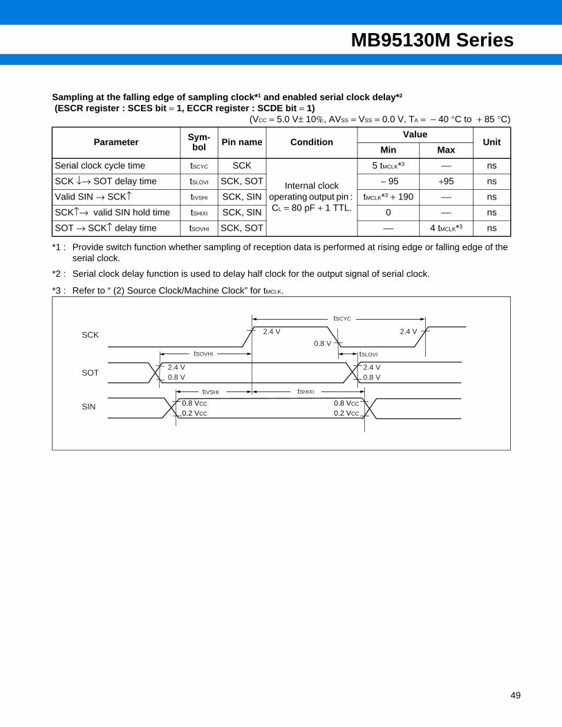
5. A/D Converter
(1) A/D Converter Electrical Characteristics (AVCC = VCC = 4.0 V to 5.5 V, AVSS = VSS = 0.0 V, TA = − 40 °C to + 85 °C)
Parameter SymbolValue
Unit RemarksMin Typ Max
Resolution
⎯
⎯ ⎯ 10 bit
Total error − 3.0 ⎯ + 3.0 LSB
Linearity error − 2.5 ⎯ + 2.5 LSB
Differential linear error
− 1.9 ⎯ + 1.9 LSB
Zero transition voltage
VOT AVSS − 1.5 LSB AVSS + 0.5 LSB AVSS + 2.5 LSB V
Full-scale transition voltage
VFST AVCC − 4.5 LSB AVCC − 1.5 LSB AVCC + 0.5 LSB V
Compare time ⎯0.9 ⎯ 16500 µs 4.5 V ≤ AVCC ≤ 5.5 V
1.8 ⎯ 16500 µs 4.0 V ≤ AVCC < 4.5 V
Sampling time ⎯
0.6 ⎯ ∞ µs4.5 V ≤ AVcc ≤ 5.5 V, At external impedance < at 5.4 kΩ
1.2 ⎯ ∞ µs4.0 V ≤ AVcc ≤ 4.5 V, At external impedance < at 2.4 kΩ
Analog input current IAIN − 0.3 ⎯ + 0.3 µA
Analog input voltage VAIN AVSS ⎯ AVCC V

MB95130M Series
(2) Notes on Using A/D Converter
• External impedance of analog input and its sampling time• A/D converter with sample and hold circuit. If the external impedance is too high to keep sufficient sampling
time, the analog voltage charged to the internal sample and hold capacitor is insufficient, adversely affectingA/D conversion precision. Therefore to satisfy the A/D conversion precision standard, consider the relationshipbetween the external impedance and minimum sampling time and either adjust the register value and operatingfrequency or decrease the external impedance so that the sampling time is longer than the minimum value.Also, if the sampling time cannot be sufficient, connect a capacitor of about 0.1 µF to the analog input pin.
• Errors
As |AVCC − AVSS| becomes smaller, values of relative errors grow larger.
R
C
Analog input
Note : The values are reference values.
• Analog input equivalent circuit
R C4.5 V ≤ AVCC ≤ 5.5 V 2.0 kΩ (Max) 16 pF (Max) 4.0 V ≤ AVCC < 4.5 V 8.2 kΩ (Max) 16 pF (Max)
Comparator
During sampling : ON
20
18
16
14
12
10
8
6
4
2
0
0 21 3 4
100
90
80
70
60
50
40
30
20
10
0
0 2 4 6 8 10 12 14
(External impedance = at 0 kΩ to 100 kΩ) (External impedance = at 0 kΩ to 20 kΩ)
Minimum sampling time [µs]
Ext
erna
l im
peda
nce
[kΩ
]
Minimum sampling time [µs]
Ext
erna
l im
peda
nce
[kΩ
]
AVCC ≥ 4.0 V
• The relationship between external impedance and minimum sampling time
AVCC ≥ 4.5 V AVCC ≥ 4.5 V
AVCC ≥ 4.0 V
53

MB95130M Series
54
(3) Definition of A/D Converter Terms• Resolution
The level of analog variation that can be distinguished by the A/D converter.When the number of bits is 10, analog voltage can be divided into 210 = 1024.
• Linearity error (unit : LSB)The deviation between the value along a straight line connecting the zero transition point (“00 0000 0000” ← → “00 0000 0001”) of a device and the full-scale transition point (“11 1111 1111” ← → “11 1111 1110”) compared with the actual conversion values obtained.
• Differential linear error (Unit : LSB) Deviation of input voltage, which is required for changing output code by 1 LSB, from an ideal value.
• Total error (unit: LSB)Difference between actual and theoretical values, caused by a zero transition error, full-scale transition error,linearity error, quantum error, and noise.
(Continued)
VFST
1.5 LSB
3FFH
3FEH
3FDH
004H
003H
002H
001H
3FFH
3FEH
3FDH
004H
003H
002H
001H
1 LSB
0.5 LSB
VOT
AVSS AVCC AVSS
VNT
AVCC
1 LSB × (N − 1) + 0.5 LSB
1 LSB = AVCC − AVSS
1024 (V) Total error of digital output N
VNT − 1 LSB × (N − 1) + 0.5 LSB1 LSB
Ideal I/O characteristics Total error
Dig
ital o
utpu
t
Analog input Analog input
Dig
ital o
utpu
t
[LSB]
Actual conversion characteristic
Actual conversion characteristic
Ideal characteristics
N : A/D converter digital output valueVNT : Voltage at which digital output transits from (N - 1) to N.
=

MB95130M Series
(Continued)
V (N + 1) T − VNT
1 LSB
AVSS AVCC
AVSS AVCC AVSS AVCC
VNT
AVSS AVCC
001H
002H
003H
004H
3FCH
3FDH
3FEH
3FFH
001H
002H
003H
004H
3FDH
3FEH
3FFH
N-2
N-1
N
N+1
1 LSB × N + VOT
VNT
V (N+1)T
Full-scale transition error
Dig
ital o
utpu
t
Actual conversion characteristics
Actual conversion characteristics
Ideal characteristics
Analog input
VFST (Actual value)
Zero transition error
Dig
ital o
utpu
t
Actual conversion characteristics
Actual conversion characteristics
Analog input
VOT (Actual value)
− 1Differential linear error of digital output N
Linear error of digital output N
VNT − 1 LSB × N + VOT1 LSB
Linearity error
Dig
ital o
utpu
t
Actual conversion characteristics
Actual conversion characteristics
Analog input
Ideal characteristics
Differential linear error
Dig
ital o
utpu
t
Actual conversion characteristics
Actual conversion characteristics
Analog input
Ideal characteristics
VFST (Actual value)
VOT (Actual value)
N : A/D converter digital output valueVNT : Voltage at which digital output transits from (N - 1) to N.VOT (Ideal value) = AVSS + 0.5 LSB [V]VFST (Ideal value) = AVCC − 1.5 LSB [V]
Ideal characteristics
= =
55

MB95130M Series
56
6. Flash Memory Program/Erase Characteristics
*1 : TA = + 25 °C, VCC = 5.0 V, 10000 cycles
*2 : TA = + 85 °C, VCC = 4.5 V, 10000 cycles
*3 : This value comes from the technology qualification (using Arrhenius equation to translate high temperature measurements into normalized value at +85 °C) .
ParameterValue
Unit RemarksMin Typ Max
Chip erase time ⎯ 1.0*1 15.0*2 s Excludes 00H programming prior erasure.
Byte programming time ⎯ 32 3600 µs Excludes system-level overhead.
Erase/program cycle 10000 ⎯ ⎯ cycle
Power supply voltage at erase/program
4.5 ⎯ 5.5 V
Flash memory data retention time
20*3 ⎯ ⎯ year Average TA = +85 °C

MB95130M Series
MASK OPTION
*: Refer to table below about clock mode select and low voltage detection reset.
No.Part number MB95136M
MB95F133MS/F133NS
MB95F134MS/F134NS
MB95F136MS/F136NS
MB95F133MW/F133NW
MB95F134MW/F134NW
MB95F136MW/F136NW
MB95FV100D-103
Specifying procedure Setting disabled
Setting disabled
Setting disabled
Setting disabled
1Clock mode select• Single-system clock mode• Dual-system clock mode
Specify whenordering MASK
Single-system clock mode
Dual-system clock mode
Changing by the switch on MCU
board
2
Low voltage detection reset*• With low voltage detection
reset• Without low voltage
detection reset
Specify whenordering MASK
Specified by part number
Specified by part number
Change by the switch on MCU
board
3Oscillation stabilizationwait time
Fixed tooscillationstabilization wait time of(214−2) /FCH
Fixed to oscillation stabilization wait time of (214-2) /FCH
Fixed to oscillation stabilization wait time of (214-2) /FCH
Fixed to oscillation stabilization wait time of (214-2) /FCH
57

MB95130M Series
58
Part number Clock mode select Low voltage detection reset
MB95136M
Single - system
No
Yes
Yes
Dual - system
No
Yes
Yes
MB95F133MS
Single - system
No
MB95F133NS Yes
MB95F134MS No
MB95F134NS Yes
MB95F136MS No
MB95F136NS Yes
MB95F133MW
Dual - system
No
MB95F133NW Yes
MB95F134MW No
MB95F134NW Yes
MB95F136MW No
MB95F136NW Yes
MB95FV100D-103
Single - system
No
Yes
Yes
Dual - system
No
Yes
Yes

MB95130M Series
ORDERING INFORMATION
Part number Package Remarks
MB95136MPFVMB95F133MSPFVMB95F133NSPFVMB95F134MSPFVMB95F134NSPFVMB95F136MSPFVMB95F136NSPFVMB95F133MWPFVMB95F133NWPFVMB95F134MWPFVMB95F134NWPFVMB95F136MWPFVMB95F136NWPFV
28-pin plastic SOP (FPT-28P-M17)
MB2146-303A (MB95FV100D-103PBT)
MCU board
( )224-pin plastic PFBGA (BGA-224P-M08)
59

MB95130M Series
60
PACKAGE DIMENSION
Please confirm the latest Package dimension by following URL.http://edevice.fujitsu.com/fj/DATASHEET/ef-ovpklv.html
28-pin plastic SOP Lead pitch 1.27 mm
Package width ×package length
8.6 × 17.75 mm
Lead shape Gullwing
Sealing method Plastic mold
Mounting height 2.80 mm MAX
Weight 0.82 g
Code(Reference)
P-SOP28-8.6×17.75-1.27
28-pin plastic SOP(FPT-28P-M17)
(FPT-28P-M17)
C 2002 FUJITSU LIMITED F28048S-c-3-4
.699 –.008+.010
–0.20+0.25
17.75
1
1.27(.050)
8.60±0.20(.339±.008)
11.80±0.30(.465±.012)
M0.13(.005)
14
1528
0.10(.004)
0.47±0.08(.019±.003)
INDEX
"A"
–0.04+0.03
0.17
.007+.001–.002
0~8˚
0.25(.010)
Details of "A" part
(Mounting height)2.65±0.15
(.104±.006)
0.20±0.15(.008±.006)(Stand off)
0.80±0.20(.031±.008)0.88±0.15
(.035±.006)
*1
*2
Dimensions in mm (inches).Note: The values in parentheses are reference values.
Note 1) *1 : These dimensions include resin protrusion.Note 2) *2 : These dimensions do not include resin protrusion.Note 3) Pins width and pins thickness include plating thickness.Note 4) Pins width do not include tie bar cutting remainder.

MB95130M Series
F0609
The information for microcontroller supports is shown in the following homepage.http://www.fujitsu.com/global/services/microelectronics/product/micom/support/index.html
FUJITSU LIMITEDAll Rights Reserved.
The contents of this document are subject to change without notice. Customers are advised to consult with FUJITSU salesrepresentatives before ordering.The information, such as descriptions of function and applicationcircuit examples, in this document are presented solely for thepurpose of reference to show examples of operations and uses ofFujitsu semiconductor device; Fujitsu does not warrant properoperation of the device with respect to use based on suchinformation. When you develop equipment incorporating thedevice based on such information, you must assume anyresponsibility arising out of such use of the information. Fujitsuassumes no liability for any damages whatsoever arising out ofthe use of the information.Any information in this document, including descriptions offunction and schematic diagrams, shall not be construed as licenseof the use or exercise of any intellectual property right, such aspatent right or copyright, or any other right of Fujitsu or any thirdparty or does Fujitsu warrant non-infringement of any third-party’sintellectual property right or other right by using such information.Fujitsu assumes no liability for any infringement of the intellectualproperty rights or other rights of third parties which would resultfrom the use of information contained herein.The products described in this document are designed, developedand manufactured as contemplated for general use, includingwithout limitation, ordinary industrial use, general office use,personal use, and household use, but are not designed, developedand manufactured as contemplated (1) for use accompanying fatalrisks or dangers that, unless extremely high safety is secured, couldhave a serious effect to the public, and could lead directly to death,personal injury, severe physical damage or other loss (i.e., nuclearreaction control in nuclear facility, aircraft flight control, air trafficcontrol, mass transport control, medical life support system, missilelaunch control in weapon system), or (2) for use requiringextremely high reliability (i.e., submersible repeater and artificialsatellite).Please note that Fujitsu will not be liable against you and/or anythird party for any claims or damages arising in connection withabove-mentioned uses of the products.Any semiconductor devices have an inherent chance of failure. Youmust protect against injury, damage or loss from such failures byincorporating safety design measures into your facility andequipment such as redundancy, fire protection, and prevention ofover-current levels and other abnormal operating conditions.If any products described in this document represent goods ortechnologies subject to certain restrictions on export under theForeign Exchange and Foreign Trade Law of Japan, the priorauthorization by Japanese government will be required for exportof those products from Japan.
Edited Business Promotion Dept.