Embed Size (px)
Citation preview
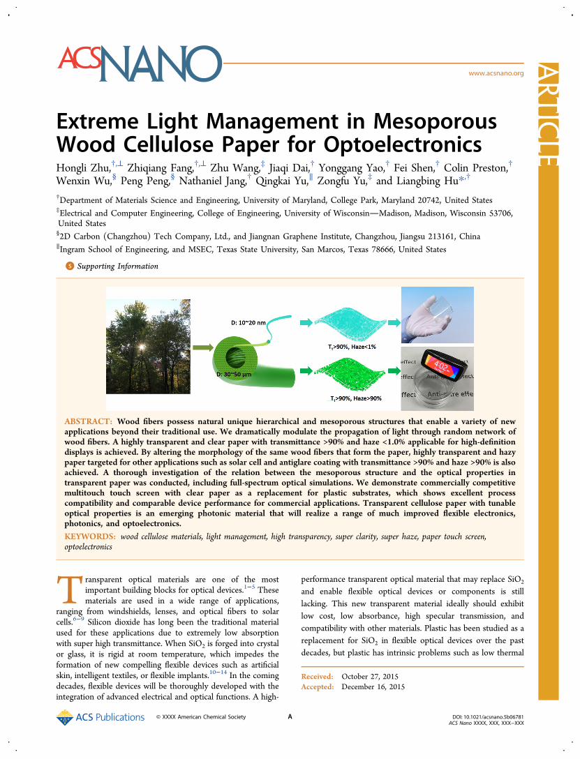
Extreme Light Management in MesoporousWood Cellulose Paper for OptoelectronicsHongli Zhu,†,⊥ Zhiqiang Fang,†,⊥ Zhu Wang,‡ Jiaqi Dai,† Yonggang Yao,† Fei Shen,† Colin Preston,†
Wenxin Wu,§ Peng Peng,§ Nathaniel Jang,† Qingkai Yu,∥ Zongfu Yu,‡ and Liangbing Hu*,†
†Department of Materials Science and Engineering, University of Maryland, College Park, Maryland 20742, United States‡Electrical and Computer Engineering, College of Engineering, University of WisconsinMadison, Madison, Wisconsin 53706,United States§2D Carbon (Changzhou) Tech Company, Ltd., and Jiangnan Graphene Institute, Changzhou, Jiangsu 213161, China∥Ingram School of Engineering, and MSEC, Texas State University, San Marcos, Texas 78666, United States
*S Supporting Information
ABSTRACT: Wood fibers possess natural unique hierarchical and mesoporous structures that enable a variety of newapplications beyond their traditional use. We dramatically modulate the propagation of light through random network ofwood fibers. A highly transparent and clear paper with transmittance >90% and haze <1.0% applicable for high-definitiondisplays is achieved. By altering the morphology of the same wood fibers that form the paper, highly transparent and hazypaper targeted for other applications such as solar cell and antiglare coating with transmittance >90% and haze >90% is alsoachieved. A thorough investigation of the relation between the mesoporous structure and the optical properties intransparent paper was conducted, including full-spectrum optical simulations. We demonstrate commercially competitivemultitouch touch screen with clear paper as a replacement for plastic substrates, which shows excellent processcompatibility and comparable device performance for commercial applications. Transparent cellulose paper with tunableoptical properties is an emerging photonic material that will realize a range of much improved flexible electronics,photonics, and optoelectronics.
KEYWORDS: wood cellulose materials, light management, high transparency, super clarity, super haze, paper touch screen,optoelectronics
Transparent optical materials are one of the mostimportant building blocks for optical devices.1−5 Thesematerials are used in a wide range of applications,
ranging from windshields, lenses, and optical fibers to solarcells.6−9 Silicon dioxide has long been the traditional materialused for these applications due to extremely low absorptionwith super high transmittance. When SiO2 is forged into crystalor glass, it is rigid at room temperature, which impedes theformation of new compelling flexible devices such as artificialskin, intelligent textiles, or flexible implants.10−14 In the comingdecades, flexible devices will be thoroughly developed with theintegration of advanced electrical and optical functions. A high-
performance transparent optical material that may replace SiO2
and enable flexible optical devices or components is stilllacking. This new transparent material ideally should exhibitlow cost, low absorbance, high specular transmission, andcompatibility with other materials. Plastic has been studied as areplacement for SiO2 in flexible optical devices over the pastdecades, but plastic has intrinsic problems such as low thermal
Received: October 27, 2015Accepted: December 16, 2015
Artic
lewww.acsnano.org
© XXXX American Chemical Society A DOI: 10.1021/acsnano.5b06781ACS Nano XXXX, XXX, XXX−XXX
stability, poor accessibility for functionalization, and harm toenvironment.15−17
Mesoporous materials are emerging toward novel photonicsand optoelectronics, through which photons can be manipu-lated to achieve desired properties.18 Note that, in thismanuscript, mesopore is defined as a nanostructure that hashierarchical pore structures from micrometer size down tonanometer size. While traditional transparent substrates such asSiO2 and plastic are solids, transparent paper is a mesoporousnetwork of cellulose nanofiber (CNF) with controllable poresizes and pore distributions.19 This type of paper photonics hastremendous potential; the mesoporous structure of cellulosefiber-based paper allows the density, pore structure, and shapeto be tuned dramatically, which is impossible to achieve withtraditional plastic substrates.20−29 It is expected, for example,that the mesopores can be filled with high index materials tocreate periodic photonic structures in paper. Mesoporous woodfiber-based paper can also be integrated in optofluidic devicesdue to the capacity to flow nanofluids through the transparentmesoporous structure. In the past few years, proof-of-conceptdevices such as transistors and solar cells have beendemonstrated on transparent paper substrates.24,30 Althoughthese devices are completely functional, the optical propertiesdo not adequately meet the desired standards. For example, theoptical clarity is critical in displays that require a haze value(indication of optical scattering) less than 1%; however, thenanopaper demonstrated with cellulose nanofibers exhibits ahaze value of around 10%, which is too high for high-definitiondisplays.31,32 A detailed understanding of the correlationbetween its structure and optical properties is still lacking.In this work, we demonstrate that large light scattering
tuning can be achieved in mesoporous paper for photonics andoptoelectronics by simply changing the packing of the cellulose
fibers. In one extreme, we achieved >90% total transmittanceand <1% optical haze, when cellulose nanofibers are denselypacked through layer by layer. In the other extreme, weachieved >90% total transmittance and >90% light scatteringwhen the microfibers are in situ nanowelded in ionic liquid. Weconducted a detailed investigation of the 3D surface topologyof mesoporous cellulose paper. This 3D topology investigationsupports a full spectrum simulation that may guide futuredesigns of transparent paper with tunable light scattering. A 2.5× 4 in.2 touch screen (multitouch) is demonstrated using dry-transferred graphene as a transparent conductor on super clearpaper. Mesoporous transparent paper with tailored opticalproperties can be applied to a range of devices resulting in anenhanced performance. Meanwhile, such super clear papershows complete process compatibility with roll-to-rollmanufacturing in flexible electronic, which is critical for futuresystem integrations for all paper photonics and optoelectronicssystems.
RESULTS AND DISCUSSION
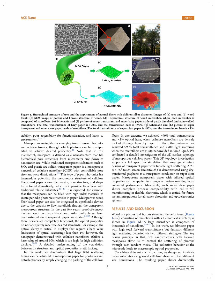
Wood is a porous and fibrous structural tissue of trees (Figure1a−c), consisting of microfibers with a hierarchical structure, asshown in Figure 1d. A large microfiber is composed ofthousands of nanofibers.33−35 In this work, we fabricate paperwith high total forward transmittance but dramatic differentlight scattering behavior via two different strategies. The keydesign principle is that rich nanostructures with tailoredmesopores allow us to control the scattering of photonsthrough such random media. The collective behavior at themicroscale leads to macroscopic optical properties.To achieve different microstructures, we design and fabricate
paper substrates using wood cellulose fibers with two differentsize dimensions. The resulting paper shows dramatically
Figure 1. Hierarchical structure of tree and the applications of natural fibers with different fiber diameter. Images of (a) tree and (b) woodtrunk. (c) SEM image of porous and fibrous structure of wood. (d) Hierarchical structure of wood microfiber, where each microfiber iscomposed of nanofibers. (e) Schematic and (f) picture of super transparent and super hazy paper made of partly dissolved and nanoweldedmicrofibers. The total transmittance of hazy paper is >90%, and the transmission haze is >90%. (g) Schematic and (h) picture of supertransparent and super clear paper made of nanofibers. The total transmittance of super clear paper is >90%, and the transmission haze is <1%.
ACS Nano Article
DOI: 10.1021/acsnano.5b06781ACS Nano XXXX, XXX, XXX−XXX
B
different optical scattering behavior. In one case, the resultedpaper is very hazy with significant amounts of mesopores and arelatively rougher surface than the clear paper (Figure 1e,f).The hazy paper is directly fabricated via nanoweldingmicrofibers in ionic liquid. These welded microfibers lead tomuch denser packing than regular paper, which dismisses thelarge air cavities (∼50 μm) and leads to the high opticaltransmittance. Meanwhile, a significant amount of mesoporesstill exist, which causes significant light scattering through the∼40−50 μm thick paper. In another case, the paper substrate issuper clear with a small quantity of mesopores and a uniformsurface texture (Figure 1g,h). The building block of the clearpaper is a purified nanofiber disintegrated from wood fiber thatexhibits a uniform size with diameter around 10−20 nm and alength around 500 nm. These nanofibers with excellentflexibility lead to a dense microstructure and optical appearanceis as clear as high-quality SiO2 glass. We significantlymanipulate the light scattering in highly transparent paper bytailoring the fiber dimensions and packing density; thecollective result is that the optical haze is adjustable betweensmaller than 1% and larger than 90% with transmittance largerthan 90%.Following the design in Figure 1g, we achieved optically clear
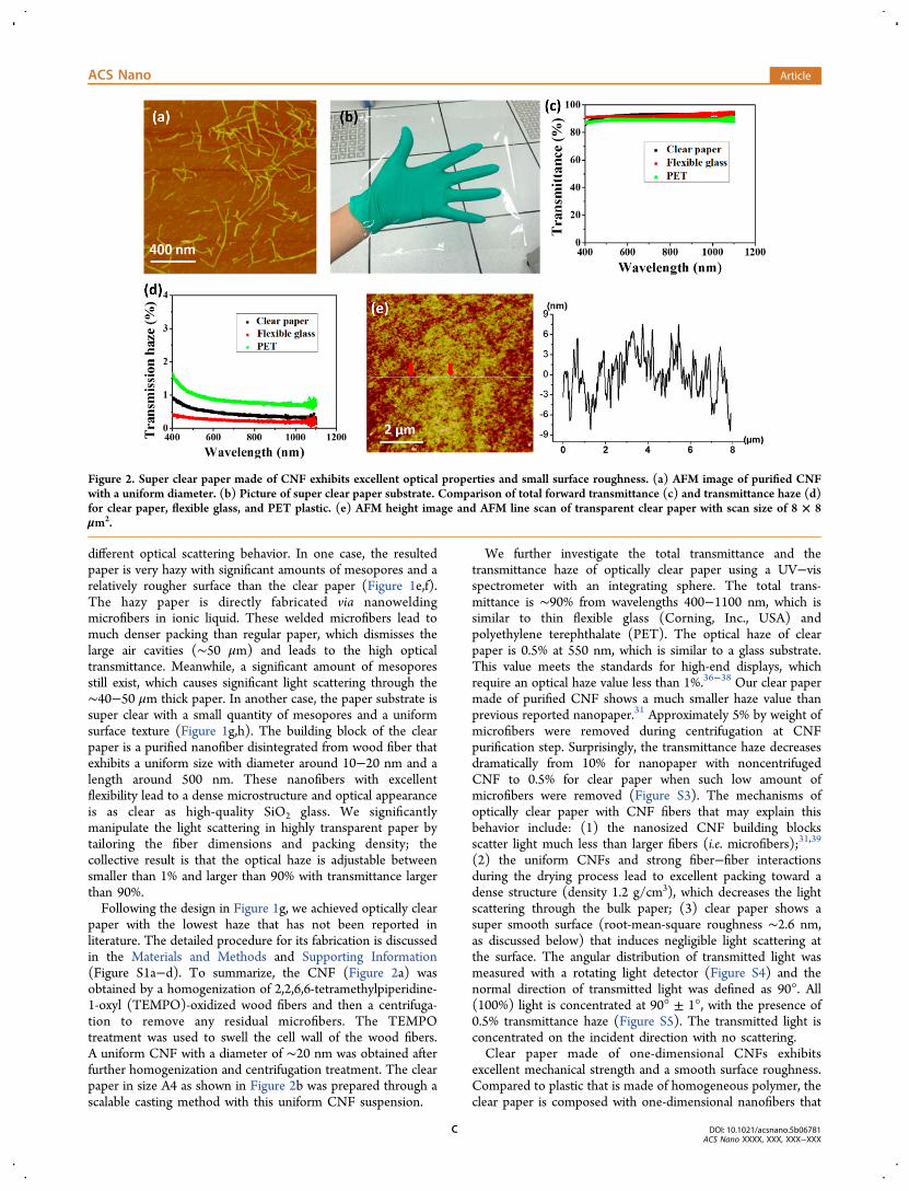
paper with the lowest haze that has not been reported inliterature. The detailed procedure for its fabrication is discussedin the Materials and Methods and Supporting Information(Figure S1a−d). To summarize, the CNF (Figure 2a) wasobtained by a homogenization of 2,2,6,6-tetramethylpiperidine-1-oxyl (TEMPO)-oxidized wood fibers and then a centrifuga-tion to remove any residual microfibers. The TEMPOtreatment was used to swell the cell wall of the wood fibers.A uniform CNF with a diameter of ∼20 nm was obtained afterfurther homogenization and centrifugation treatment. The clearpaper in size A4 as shown in Figure 2b was prepared through ascalable casting method with this uniform CNF suspension.
We further investigate the total transmittance and thetransmittance haze of optically clear paper using a UV−visspectrometer with an integrating sphere. The total trans-mittance is ∼90% from wavelengths 400−1100 nm, which issimilar to thin flexible glass (Corning, Inc., USA) andpolyethylene terephthalate (PET). The optical haze of clearpaper is 0.5% at 550 nm, which is similar to a glass substrate.This value meets the standards for high-end displays, whichrequire an optical haze value less than 1%.36−38 Our clear papermade of purified CNF shows a much smaller haze value thanprevious reported nanopaper.31 Approximately 5% by weight ofmicrofibers were removed during centrifugation at CNFpurification step. Surprisingly, the transmittance haze decreasesdramatically from 10% for nanopaper with noncentrifugedCNF to 0.5% for clear paper when such low amount ofmicrofibers were removed (Figure S3). The mechanisms ofoptically clear paper with CNF fibers that may explain thisbehavior include: (1) the nanosized CNF building blocksscatter light much less than larger fibers (i.e. microfibers);31,39
(2) the uniform CNFs and strong fiber−fiber interactionsduring the drying process lead to excellent packing toward adense structure (density 1.2 g/cm3), which decreases the lightscattering through the bulk paper; (3) clear paper shows asuper smooth surface (root-mean-square roughness ∼2.6 nm,as discussed below) that induces negligible light scattering atthe surface. The angular distribution of transmitted light wasmeasured with a rotating light detector (Figure S4) and thenormal direction of transmitted light was defined as 90°. All(100%) light is concentrated at 90° ± 1°, with the presence of0.5% transmittance haze (Figure S5). The transmitted light isconcentrated on the incident direction with no scattering.Clear paper made of one-dimensional CNFs exhibits
excellent mechanical strength and a smooth surface roughness.Compared to plastic that is made of homogeneous polymer, theclear paper is composed with one-dimensional nanofibers that
Figure 2. Super clear paper made of CNF exhibits excellent optical properties and small surface roughness. (a) AFM image of purified CNFwith a uniform diameter. (b) Picture of super clear paper substrate. Comparison of total forward transmittance (c) and transmittance haze (d)for clear paper, flexible glass, and PET plastic. (e) AFM height image and AFM line scan of transparent clear paper with scan size of 8 × 8μm2.
ACS Nano Article
DOI: 10.1021/acsnano.5b06781ACS Nano XXXX, XXX, XXX−XXX
C
possess rich hydroxyl groups. Coupled with the outstandingmechanical properties of individual CNFs (Young’s Modulus150 GPa of cellulose nanocrystal),40,41 the network structurelinked by strong hydrogen bonds between CNFs leads to bothexcellent mechanical strength and flexibility in clear paper(Figure S6a,b). Surprisingly, the mesoporous clear paper with anetwork structure has a small surface roughness, as shown inFigure 2e. The atomic force microscope (AFM) topographicalline scan reveals root-mean-square (RMS) roughness of 2.6 nm.We also invented a simple and fast in situ pressing method
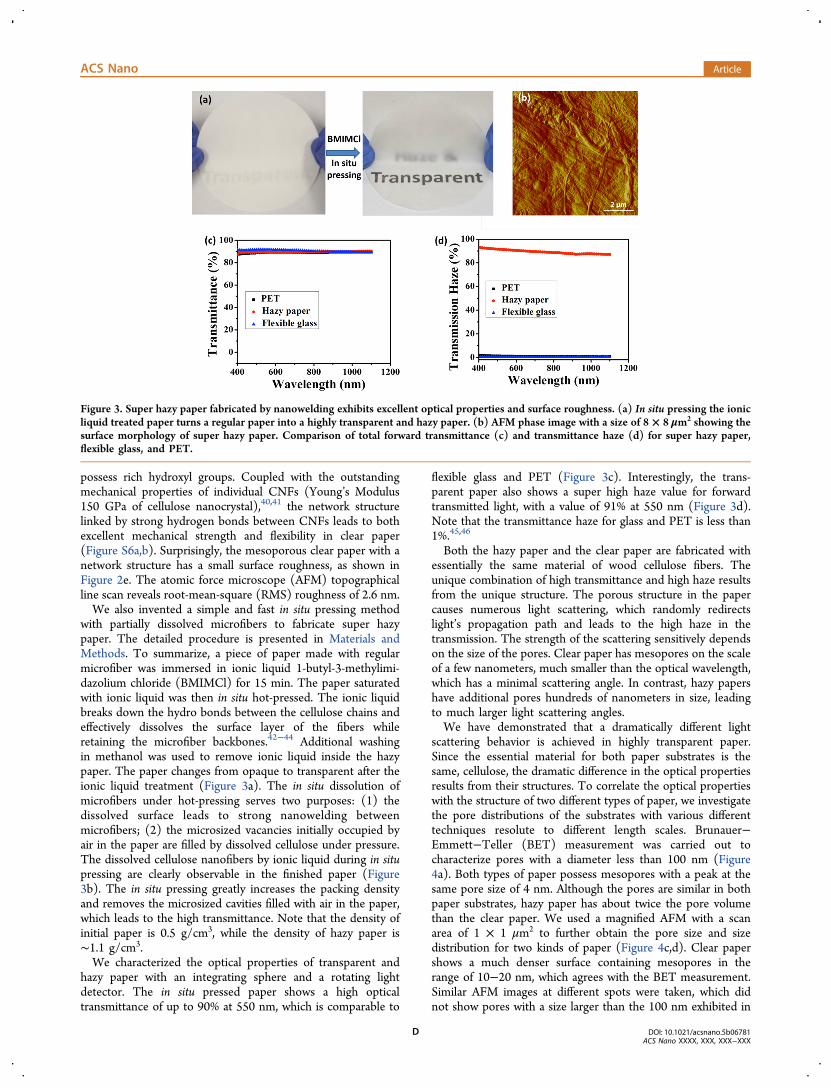
with partially dissolved microfibers to fabricate super hazypaper. The detailed procedure is presented in Materials andMethods. To summarize, a piece of paper made with regularmicrofiber was immersed in ionic liquid 1-butyl-3-methylimi-dazolium chloride (BMIMCl) for 15 min. The paper saturatedwith ionic liquid was then in situ hot-pressed. The ionic liquidbreaks down the hydro bonds between the cellulose chains andeffectively dissolves the surface layer of the fibers whileretaining the microfiber backbones.42−44 Additional washingin methanol was used to remove ionic liquid inside the hazypaper. The paper changes from opaque to transparent after theionic liquid treatment (Figure 3a). The in situ dissolution ofmicrofibers under hot-pressing serves two purposes: (1) thedissolved surface leads to strong nanowelding betweenmicrofibers; (2) the microsized vacancies initially occupied byair in the paper are filled by dissolved cellulose under pressure.The dissolved cellulose nanofibers by ionic liquid during in situpressing are clearly observable in the finished paper (Figure3b). The in situ pressing greatly increases the packing densityand removes the microsized cavities filled with air in the paper,which leads to the high transmittance. Note that the density ofinitial paper is 0.5 g/cm3, while the density of hazy paper is∼1.1 g/cm3.We characterized the optical properties of transparent and
hazy paper with an integrating sphere and a rotating lightdetector. The in situ pressed paper shows a high opticaltransmittance of up to 90% at 550 nm, which is comparable to
flexible glass and PET (Figure 3c). Interestingly, the trans-parent paper also shows a super high haze value for forwardtransmitted light, with a value of 91% at 550 nm (Figure 3d).Note that the transmittance haze for glass and PET is less than1%.45,46
Both the hazy paper and the clear paper are fabricated withessentially the same material of wood cellulose fibers. Theunique combination of high transmittance and high haze resultsfrom the unique structure. The porous structure in the papercauses numerous light scattering, which randomly redirectslight’s propagation path and leads to the high haze in thetransmission. The strength of the scattering sensitively dependson the size of the pores. Clear paper has mesopores on the scaleof a few nanometers, much smaller than the optical wavelength,which has a minimal scattering angle. In contrast, hazy papershave additional pores hundreds of nanometers in size, leadingto much larger light scattering angles.We have demonstrated that a dramatically different light
scattering behavior is achieved in highly transparent paper.Since the essential material for both paper substrates is thesame, cellulose, the dramatic difference in the optical propertiesresults from their structures. To correlate the optical propertieswith the structure of two different types of paper, we investigatethe pore distributions of the substrates with various differenttechniques resolute to different length scales. Brunauer−Emmett−Teller (BET) measurement was carried out tocharacterize pores with a diameter less than 100 nm (Figure4a). Both types of paper possess mesopores with a peak at thesame pore size of 4 nm. Although the pores are similar in bothpaper substrates, hazy paper has about twice the pore volumethan the clear paper. We used a magnified AFM with a scanarea of 1 × 1 μm2 to further obtain the pore size and sizedistribution for two kinds of paper (Figure 4c,d). Clear papershows a much denser surface containing mesopores in therange of 10−20 nm, which agrees with the BET measurement.Similar AFM images at different spots were taken, which didnot show pores with a size larger than the 100 nm exhibited in
Figure 3. Super hazy paper fabricated by nanowelding exhibits excellent optical properties and surface roughness. (a) In situ pressing the ionicliquid treated paper turns a regular paper into a highly transparent and hazy paper. (b) AFM phase image with a size of 8 × 8 μm2 showing thesurface morphology of super hazy paper. Comparison of total forward transmittance (c) and transmittance haze (d) for super hazy paper,flexible glass, and PET.
ACS Nano Article
DOI: 10.1021/acsnano.5b06781ACS Nano XXXX, XXX, XXX−XXX
D
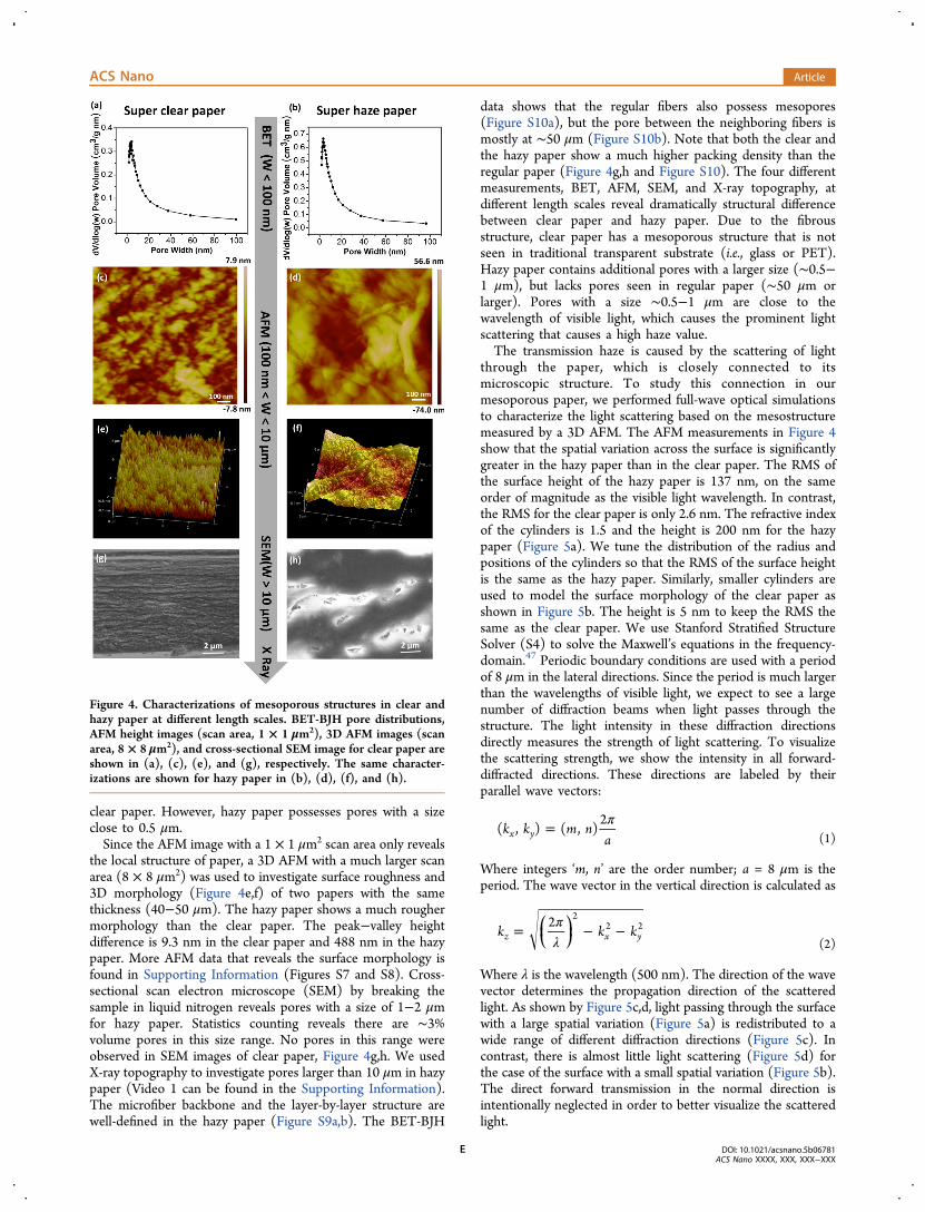
clear paper. However, hazy paper possesses pores with a sizeclose to 0.5 μm.Since the AFM image with a 1 × 1 μm2 scan area only reveals
the local structure of paper, a 3D AFM with a much larger scanarea (8 × 8 μm2) was used to investigate surface roughness and3D morphology (Figure 4e,f) of two papers with the samethickness (40−50 μm). The hazy paper shows a much roughermorphology than the clear paper. The peak−valley heightdifference is 9.3 nm in the clear paper and 488 nm in the hazypaper. More AFM data that reveals the surface morphology isfound in Supporting Information (Figures S7 and S8). Cross-sectional scan electron microscope (SEM) by breaking thesample in liquid nitrogen reveals pores with a size of 1−2 μmfor hazy paper. Statistics counting reveals there are ∼3%volume pores in this size range. No pores in this range wereobserved in SEM images of clear paper, Figure 4g,h. We usedX-ray topography to investigate pores larger than 10 μm in hazypaper (Video 1 can be found in the Supporting Information).The microfiber backbone and the layer-by-layer structure arewell-defined in the hazy paper (Figure S9a,b). The BET-BJH
data shows that the regular fibers also possess mesopores(Figure S10a), but the pore between the neighboring fibers ismostly at ∼50 μm (Figure S10b). Note that both the clear andthe hazy paper show a much higher packing density than theregular paper (Figure 4g,h and Figure S10). The four differentmeasurements, BET, AFM, SEM, and X-ray topography, atdifferent length scales reveal dramatically structural differencebetween clear paper and hazy paper. Due to the fibrousstructure, clear paper has a mesoporous structure that is notseen in traditional transparent substrate (i.e., glass or PET).Hazy paper contains additional pores with a larger size (∼0.5−1 μm), but lacks pores seen in regular paper (∼50 μm orlarger). Pores with a size ∼0.5−1 μm are close to thewavelength of visible light, which causes the prominent lightscattering that causes a high haze value.The transmission haze is caused by the scattering of light
through the paper, which is closely connected to itsmicroscopic structure. To study this connection in ourmesoporous paper, we performed full-wave optical simulationsto characterize the light scattering based on the mesostructuremeasured by a 3D AFM. The AFM measurements in Figure 4show that the spatial variation across the surface is significantlygreater in the hazy paper than in the clear paper. The RMS ofthe surface height of the hazy paper is 137 nm, on the sameorder of magnitude as the visible light wavelength. In contrast,the RMS for the clear paper is only 2.6 nm. The refractive indexof the cylinders is 1.5 and the height is 200 nm for the hazypaper (Figure 5a). We tune the distribution of the radius andpositions of the cylinders so that the RMS of the surface heightis the same as the hazy paper. Similarly, smaller cylinders areused to model the surface morphology of the clear paper asshown in Figure 5b. The height is 5 nm to keep the RMS thesame as the clear paper. We use Stanford Stratified StructureSolver (S4) to solve the Maxwell’s equations in the frequency-domain.47 Periodic boundary conditions are used with a periodof 8 μm in the lateral directions. Since the period is much largerthan the wavelengths of visible light, we expect to see a largenumber of diffraction beams when light passes through thestructure. The light intensity in these diffraction directionsdirectly measures the strength of light scattering. To visualizethe scattering strength, we show the intensity in all forward-diffracted directions. These directions are labeled by theirparallel wave vectors:
π=k k m na
( , ) ( , )2
x y (1)
Where integers ‘m, n’ are the order number; a = 8 μm is theperiod. The wave vector in the vertical direction is calculated as
πλ
= − −⎜ ⎟⎛⎝
⎞⎠k k k
2z x y
22 2
(2)
Where λ is the wavelength (500 nm). The direction of the wavevector determines the propagation direction of the scatteredlight. As shown by Figure 5c,d, light passing through the surfacewith a large spatial variation (Figure 5a) is redistributed to awide range of different diffraction directions (Figure 5c). Incontrast, there is almost little light scattering (Figure 5d) forthe case of the surface with a small spatial variation (Figure 5b).The direct forward transmission in the normal direction isintentionally neglected in order to better visualize the scatteredlight.
Figure 4. Characterizations of mesoporous structures in clear andhazy paper at different length scales. BET-BJH pore distributions,AFM height images (scan area, 1 × 1 μm2), 3D AFM images (scanarea, 8 × 8 μm2), and cross-sectional SEM image for clear paper areshown in (a), (c), (e), and (g), respectively. The same character-izations are shown for hazy paper in (b), (d), (f), and (h).
ACS Nano Article
DOI: 10.1021/acsnano.5b06781ACS Nano XXXX, XXX, XXX−XXX
E
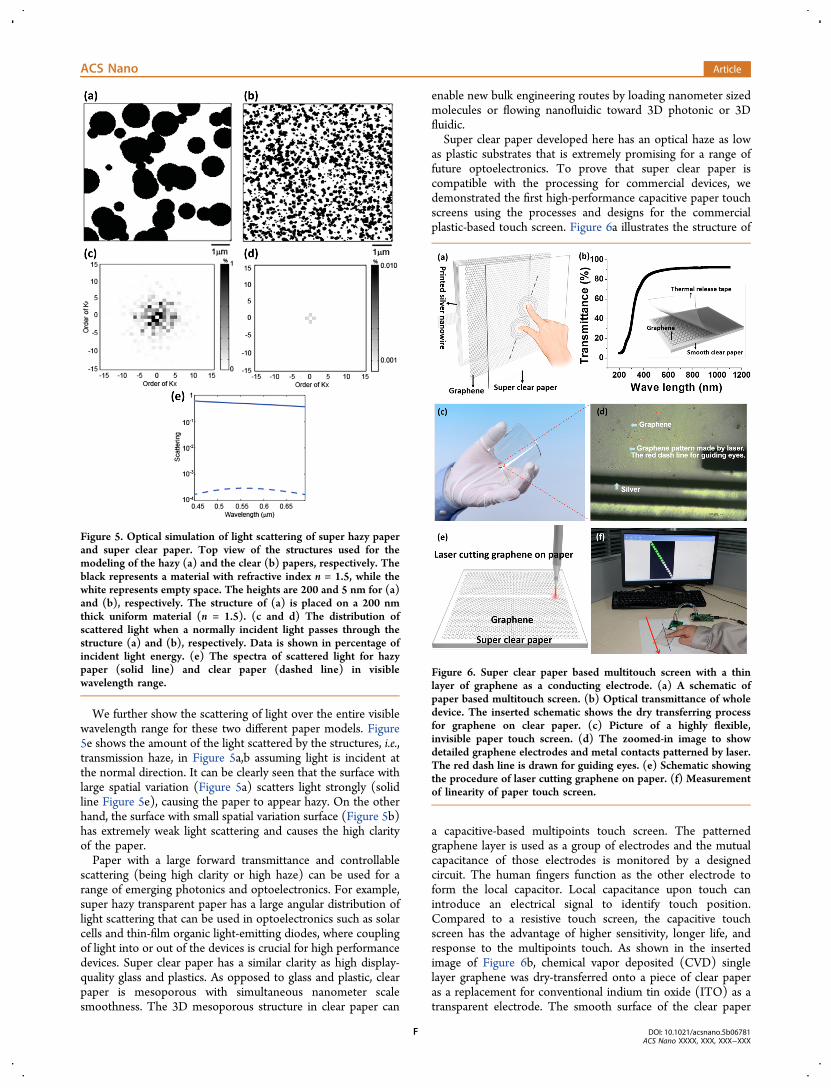
We further show the scattering of light over the entire visiblewavelength range for these two different paper models. Figure5e shows the amount of the light scattered by the structures, i.e.,transmission haze, in Figure 5a,b assuming light is incident atthe normal direction. It can be clearly seen that the surface withlarge spatial variation (Figure 5a) scatters light strongly (solidline Figure 5e), causing the paper to appear hazy. On the otherhand, the surface with small spatial variation surface (Figure 5b)has extremely weak light scattering and causes the high clarityof the paper.Paper with a large forward transmittance and controllable
scattering (being high clarity or high haze) can be used for arange of emerging photonics and optoelectronics. For example,super hazy transparent paper has a large angular distribution oflight scattering that can be used in optoelectronics such as solarcells and thin-film organic light-emitting diodes, where couplingof light into or out of the devices is crucial for high performancedevices. Super clear paper has a similar clarity as high display-quality glass and plastics. As opposed to glass and plastic, clearpaper is mesoporous with simultaneous nanometer scalesmoothness. The 3D mesoporous structure in clear paper can
enable new bulk engineering routes by loading nanometer sizedmolecules or flowing nanofluidic toward 3D photonic or 3Dfluidic.Super clear paper developed here has an optical haze as low
as plastic substrates that is extremely promising for a range offuture optoelectronics. To prove that super clear paper iscompatible with the processing for commercial devices, wedemonstrated the first high-performance capacitive paper touchscreens using the processes and designs for the commercialplastic-based touch screen. Figure 6a illustrates the structure of
a capacitive-based multipoints touch screen. The patternedgraphene layer is used as a group of electrodes and the mutualcapacitance of those electrodes is monitored by a designedcircuit. The human fingers function as the other electrode toform the local capacitor. Local capacitance upon touch canintroduce an electrical signal to identify touch position.Compared to a resistive touch screen, the capacitive touchscreen has the advantage of higher sensitivity, longer life, andresponse to the multipoints touch. As shown in the insertedimage of Figure 6b, chemical vapor deposited (CVD) singlelayer graphene was dry-transferred onto a piece of clear paperas a replacement for conventional indium tin oxide (ITO) as atransparent electrode. The smooth surface of the clear paper
Figure 5. Optical simulation of light scattering of super hazy paperand super clear paper. Top view of the structures used for themodeling of the hazy (a) and the clear (b) papers, respectively. Theblack represents a material with refractive index n = 1.5, while thewhite represents empty space. The heights are 200 and 5 nm for (a)and (b), respectively. The structure of (a) is placed on a 200 nmthick uniform material (n = 1.5). (c and d) The distribution ofscattered light when a normally incident light passes through thestructure (a) and (b), respectively. Data is shown in percentage ofincident light energy. (e) The spectra of scattered light for hazypaper (solid line) and clear paper (dashed line) in visiblewavelength range.
Figure 6. Super clear paper based multitouch screen with a thinlayer of graphene as a conducting electrode. (a) A schematic ofpaper based multitouch screen. (b) Optical transmittance of wholedevice. The inserted schematic shows the dry transferring processfor graphene on clear paper. (c) Picture of a highly flexible,invisible paper touch screen. (d) The zoomed-in image to showdetailed graphene electrodes and metal contacts patterned by laser.The red dash line is drawn for guiding eyes. (e) Schematic showingthe procedure of laser cutting graphene on paper. (f) Measurementof linearity of paper touch screen.
ACS Nano Article
DOI: 10.1021/acsnano.5b06781ACS Nano XXXX, XXX, XXX−XXX
F
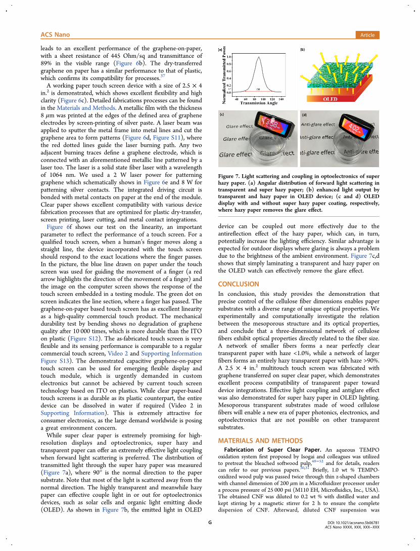
leads to an excellent performance of the graphene-on-paper,with a sheet resistance of 445 Ohm/sq and transmittance of89% in the visible range (Figure 6b). The dry-transferredgraphene on paper has a similar performance to that of plastic,which confirms its compatibility for processes.37
A working paper touch screen device with a size of 2.5 × 4in.2 is demonstrated, which shows excellent flexibility and highclarity (Figure 6c). Detailed fabrications processes can be foundin the Materials and Methods. A metallic film with the thickness8 μm was printed at the edges of the defined area of grapheneelectrodes by screen-printing of silver paste. A laser beam wasapplied to sputter the metal frame into metal lines and cut thegraphene area to form patterns (Figure 6d, Figure S11), wherethe red dotted lines guide the laser burning path. Any twoadjacent burning traces define a graphene electrode, which isconnected with an aforementioned metallic line patterned by alaser too. The laser is a solid state fiber laser with a wavelengthof 1064 nm. We used a 2 W laser power for patterninggraphene which schematically shows in Figure 6e and 8 W forpatterning silver contacts. The integrated driving circuit isbonded with metal contacts on paper at the end of the module.Clear paper shows excellent compatibility with various devicefabrication processes that are optimized for plastic dry-transfer,screen printing, laser cutting, and metal contact integrations.Figure 6f shows our test on the linearity, an important
parameter to reflect the performance of a touch screen. For aqualified touch screen, when a human’s finger moves along astraight line, the device incorporated with the touch screenshould respond to the exact locations where the finger passes.In the picture, the blue line drawn on paper under the touchscreen was used for guiding the movement of a finger (a redarrow highlights the direction of the movement of a finger) andthe image on the computer screen shows the response of thetouch screen embedded in a testing module. The green dot onscreen indicates the line section, where a finger has passed. Thegraphene-on-paper based touch screen has as excellent linearityas a high-quality commercial touch product. The mechanicaldurability test by bending shows no degradation of graphenequality after 10 000 times, which is more durable than the ITOon plastic (Figure S12). The as-fabricated touch screen is veryflexible and its sensing performance is comparable to a regularcommercial touch screen, Video 2 and Supporting InformationFigure S13). The demonstrated capacitive graphene-on-papertouch screen can be used for emerging flexible display andtouch module, which is urgently demanded in customelectronics but cannot be achieved by current touch screentechnology based on ITO on plastics. While clear paper-basedtouch screens is as durable as its plastic counterpart, the entiredevice can be dissolved in water if required (Video 2 inSupporting Information). This is extremely attractive forconsumer electronics, as the large demand worldwide is posinga great environment concern.While super clear paper is extremely promising for high-
resolution displays and optoelectronics, super hazy andtransparent paper can offer an extremely effective light couplingwhen forward light scattering is preferred. The distribution oftransmitted light through the super hazy paper was measured(Figure 7a), where 90° is the normal direction to the papersubstrate. Note that most of the light is scattered away from thenormal direction. The highly transparent and meanwhile hazypaper can effective couple light in or out for optoelectronicsdevices, such as solar cells and organic light emitting diode(OLED). As shown in Figure 7b, the emitted light in OLED
device can be coupled out more effectively due to theantireflection effect of the hazy paper, which can, in turn,potentially increase the lighting efficiency. Similar advantage isexpected for outdoor displays where glaring is always a problemdue to the brightness of the ambient environment. Figure 7c,dshows that simply laminating a transparent and hazy paper onthe OLED watch can effectively remove the glare effect.
CONCLUSIONIn conclusion, this study provides the demonstration thatprecise control of the cellulose fiber dimensions enables papersubstrates with a diverse range of unique optical properties. Weexperimentally and computationally investigate the relationbetween the mesoporous structure and its optical properties,and conclude that a three-dimensional network of cellulosefibers exhibit optical properties directly related to the fiber size.A network of smaller fibers forms a near perfectly cleartransparent paper with haze <1.0%, while a network of largerfibers forms an entirely hazy transparent paper with haze >90%.A 2.5 × 4 in.2 multitouch touch screen was fabricated withgraphene transferred on super clear paper, which demonstratesexcellent process compatibility of transparent paper towarddevice integrations. Effective light coupling and antiglare effectwas also demonstrated for super hazy paper in OLED lighting.Mesoporous transparent substrates made of wood cellulosefibers will enable a new era of paper photonics, electronics, andoptoelectronics that are not possible on other transparentsubstrates.
MATERIALS AND METHODSFabrication of Super Clear Paper. An aqueous TEMPO
oxidation system first proposed by Isogai and colleagues was utilizedto pretreat the bleached softwood pulp,48−52 and for details, readerscan refer to our previous papers.30,31 Briefly, 1.0 wt % TEMPO-oxidized wood pulp was passed twice through thin z-shaped chamberswith channel dimension of 200 μm in a Microfluidizer processor undera process pressure of 25 000 psi (M110 EH, Microfluidics, Inc., USA).The obtained CNF was diluted to 0.2 wt % with distilled water andkept stirring by a magnetic stirrer for 2 h to ensure the completedispersion of CNF. Afterward, diluted CNF suspension was
Figure 7. Light scattering and coupling in optoelectronics of superhazy paper. (a) Angular distribution of forward light scattering intransparent and super hazy paper; (b) enhanced light output bytransparent and hazy paper in OLED device; (c and d) OLEDdisplay with and without super hazy paper coating, respectively,where hazy paper removes the glare effect.
ACS Nano Article
DOI: 10.1021/acsnano.5b06781ACS Nano XXXX, XXX, XXX−XXX
G
centrifuged at the speed of 3000 rpm/min for 20 min to remove largecellulose bundles. The supernatant was transferred into a bottle viapipet. The purified CNF suspension was poured into a nonstickcontainer and dried in a controlled chamber.Fabrication of Super Hazy Paper. A regular paper with a
thickness around 90 μm was fabricated by a vacuum filtration methodwith a well-dispersed suspension of southern yellow pine fiber. Thedried sheet was immersed in BMIMCl ionic liquid at 90 °C for 15 minand then transferred to a hot-press for an additional 1 h treatment.After that, the sample was immersed in methanol (Sigma-Aldrich,USA) for 8 h to remove ionic liquid residue. After a rinsing step, thepaper sheet was cold pressed and dried. The final paper has thicknessof ∼40 μm.Fabrication of Touch Screen Graphene-on-Clear Paper. The
fabrication process of the super clear paper/graphene touch screen isdescribed below: (1) Graphene was grown on a Cu foil by CVD usingmethane as a precursor at 1030 °C. (2) For transferring graphene tosuper clear paper, thermal release tape was applied on the front side ofgraphene/Cu structure first, then oxygen plasma was used to etch thegraphene at the back side of graphene/Cu structure, followed bydissolving the Cu foil in Fe(NO3)3. The thermal release tape/graphenestructure was then laid on a super clear paper and heated at 100 °C torelease the graphene from the thermal release tape onto the super clearpaper, as illustrated in the inset image in Figure 6b. (3) The bilayerstructure of graphene/clear paper was used to fabricate capacitivetouch screens, where the graphene film was patterned as a group ofelectrodes.Characterization. The optical properties of the paper were
measured using a UV−vis Spectrometer Lambda 35 containing anintegrating sphere (PerkInElmer, USA) based on standardASTM1003-92 “Standard Method for Haze and Luminous Trans-mittance of Transparent Plastic”. Surface characterization wasperformed using a Veeco multimode scanning probe microscope(SPM) with NanoScope V controller with a model SNL-10 silicon-on-nitride tip (Veeco) using a drive frequency of ∼75 kHz and a springconstant of 0.58 N/m. Prior to imaging, paper samples were mountedon magnetic sample disks using double-sided tap. Scans were collectedover areas ranging from 500 nm2 to 8 μm2 at a scan rates of 0.46−0.92Hz. Image data were processed by planar background subtractionusing Nanoscope Analysis software, version 1.4 (Bruker). Partiallydissolved paper was characterized with a Hitachi SU-70 FESEM fieldeffect scanning electron microscopy (SEM), performed using a JeolJXA 840A system (Jeol Instruments, Tokyo, Japan) running at 5−10keV. The paper surface area was measured with a MicromeriticsTriStar II 3020 Porosimeter Test Station. The paper pore distributionwas measured with a Micromeritics TriStar II 3020 Porosimeter TestStation. The range of measurable pore sizes is between 1.7 and 120nm. The Barrett−Joyner−Halenda (BJH) adsorption average porealgorithm is used for evaluation. The hazy paper was tested in aSkyscan 1172 μCT for morphology analysis. The sample was scannedwithout a filter under 40 kV at 1.0 um pixels. The 3D images werereconstructed in NRecon. Touch screen performance was tested onTP Tool SIU board module operated by software FT Touch Studio.
ASSOCIATED CONTENT*S Supporting InformationThe Supporting Information is available free of charge on theACS Publications website at DOI: 10.1021/acsnano.5b06781.
The procedures for preparing super clear paper, the AFMimage of CNF for super clear paper, the transmissionhaze of super clear paper with/without purification ofCNF suspension in the visible wavelength, schematicshowing the measurement setup for angular dependenttransmittance, angular distribution of forwarded lightscattering of super clear paper, stress−strain curve ofsuper clear paper and ultra hazy paper, X-ray topographyof the super hazy paper, BET pore distribution andmorphology of regular paper, laser patterning of
graphene-on-paper, the durability and performance ofsuper clear paper based touch screen (PDF)Movie 1: X-ray topography (AVI)Movie 2: Touch screen (AVI)
AUTHOR INFORMATIONCorresponding Author*E-mail: [email protected] Contributions⊥H.Z. and Z.F. contributed equally to this work.NotesThe authors declare no competing financial interest.
ACKNOWLEDGMENTSL. Hu acknowledges the support from the DOD (Air Force ofScientific Research) Young Invest igator Program(FA95501310143). We acknowledge Peter Ciesielski in theNational Bioenergy Center at National Renewable EnergyLaboratory (Golden, CO) for helping us on the AFM images.Zhiqiang Fang would like to thank the China ScholarshipCouncil (CSC) for their financial support.
REFERENCES(1) Wu, H.; Kong, D. S.; Ruan, Z. C.; Hsu, P. C.; Wang, S.; Yu, Z. F.;Carney, T. J.; Hu, L. B.; Fan, S. H.; Cui, Y. A transparent electrodebased on a metal nanotrough network. Nat. Nanotechnol. 2013, 8,421−425.(2) Ben-Sasson, A. J.; Tessler, N. Unraveling the physics of verticalorganic field effect transistors through nanoscale engineering of a self-assembled transparent electrode. Nano Lett. 2012, 12, 4729−33.(3) Xia, Y.; Sun, K.; Ouyang, J. Solution-processed metallicconducting polymer films as transparent electrode of optoelectronicdevices. Adv. Mater. 2012, 24, 2436−2440.(4) Hu, L. B.; Hecht, D. S.; Gruner, G. Carbon Nanotube ThinFilms, Fabrication, Properties, and Applications. Chem. Rev. 2010, 110,5790−5844.(5) Zhang, C.; Zhao, D.; Gu, D.; Kim, H.; Ling, T.; Wu, Y. K.; Guo,L. J. An Ultrathin, Smooth, and Low-Loss Al-doped Ag Film and ItsApplication as A Transparent Electrode in Oganic Photovoltaics. Adv.Mater. 2014, 26, 5696−5701.(6) Keiser, G. Optical Fiber Communications. Wiley Encyclopedia ofTelecommunications; John Wiley & Sons, Inc., 2003.(7) Wang, X.; Zhi, L.; Mullen, K. Transparent, Conductive GrapheneElectrodes for Dye-Sensitized Solar Cells. Nano Lett. 2008, 8, 323−327.(8) Wang, B.; Ye, M.; Sato, S. Lens of Electrically Controllable FocalLength Made by a Glass Lens and Liquid-Crystal Layers. Appl. Opt.2004, 43, 3420−3425.(9) Wu, J.; Becerril, H. A.; Bao, Z.; Liu, Z.; Chen, Y.; Peumans, P.Organic Solar Cells with Solution-processed Graphene TransparentElectrodes. Appl. Phys. Lett. 2008, 92, 263302.(10) Someya, T.; Sekitani, T.; Iba, S.; Kato, Y.; Kawaguchi, H.;Sakurai, T. A Large-Area, Flexible Pressure Sensor Matrix with OrganicField-Effect Transistors for Artificial Skin Applications. Proc. Natl.Acad. Sci. U. S. A. 2004, 101, 9966−9970.(11) Katragadda, R. B.; Xu, Y. A Novel Intelligent TextileTechnology Based on Silicon Flexible Skins. Sens. Actuators, A 2008,143, 169−174.(12) Najafi, K.; Wise, K. D. An Implantable Multielectrode Arraywith On-Chip Signal Processing. IEEE J. Solid-State Circuits 1986, 21,1035−1044.(13) Kim, D. H.; Kim, Y. S.; Amsden, J.; Panilaitis, B.; Kaplan, D. L.;Omenetto, F. G.; Zakin, M. R.; Rogers, J. A. Silicon Electronics on Silkas A Path to Bioresorbable, Implantable Devices. Appl. Phys. Lett.2009, 95, 133701.
ACS Nano Article
DOI: 10.1021/acsnano.5b06781ACS Nano XXXX, XXX, XXX−XXX
H
(14) Berger, T. W.; Baudry, M.; Brinton, R. D.; Liaw, J. S.;Marmarelis, V. Z.; Yoondong Park, A.; Sheu, B. J.; Tanguay, A. R.Brain-Implantable Biomimetic Electronics as the Next Era in NeuralProsthetics. Proc. IEEE 2001, 89, 993−1012.(15) McAlpine, M. C.; Ahmad, H.; Wang, D.; Heath, J. R. HighlyOrdered Nanowire Arrays on Plastic Substrates for UltrasensitiveFlexible Chemical Sensors. Nat. Mater. 2007, 6, 379−384.(16) Kim, D.-H.; Kim, Y.-S.; Wu, J.; Liu, Z.; Song, J.; Kim, H.-S.;Huang, Y. Y.; Hwang, K.-C.; Rogers, J. A. Ultrathin Silicon CircuitsWith Strain-Isolation Layers and Mesh Layouts for High-PerformanceElectronics on Fabric, Vinyl, Leather, and Paper. Adv. Mater. 2009, 21,3703−3707.(17) Mohanty, A. K.; Misra, M.; Drzal, L. T. Sustainable Bio-Composites from Renewable Resources, Opportunities and Challengesin the Green Materials World. J. Polym. Environ. 2002, 10, 19−26.(18) Khan, M. K.; Giese, M.; Yu, M.; Kelly, J. A.; Hamad, W. Y.;MacLachlan, M. J. Flexible Mesoporous Photonic Resins with TunableChiral Nematic Structures. Angew. Chem., Int. Ed. 2013, 52, 8921−8924.(19) Sehaqui, H.; Zhou, Q.; Ikkala, O.; Berglund, L. A. Strong andTough Cellulose Nanopaper with High Specific Surface Area andPorosity. Biomacromolecules 2011, 12, 3638−3644.(20) Yousefi, H.; Faezipour, M.; Nishino, T.; Shakeri, A.; Ebrahimi,G. All-Cellulose Composite and Nanocomposite Made from PartiallyDissolved Micro-and Nanofibers of Canola Straw. Polym. J. 2011, 43,559−564.(21) Nishino, T.; Matsuda, I.; Hirao, K. All-Cellulose Composite.Macromolecules 2004, 37, 7683−7687.(22) Horiuchi, N. Optical materials: Nanostructured Paper. Nat.Photonics 2014, 8, 172−172.(23) Svagan, A. J.; Busko, D.; Avlasevich, Y.; Glasser, G.; Baluschev,S.; Landfester, K. Photon Energy Upconverting Nanopaper: ABioinspired Oxygen Protection Strategy. ACS Nano 2014, 8, 8198−8207.(24) Fang, Z.; Zhu, H.; Yuan, Y.; Ha, D.; Zhu, S.; Preston, C.; Chen,Q.; Li, Y.; Han, X.; Lee, S.; et al. Novel Nanostructured Paper withUltrahigh Transparency and Ultrahigh Haze for Solar Cells. Nano Lett.2014, 14, 765−773.(25) Nakagaito, A. N.; Nogi, M.; Yano, H. Displays from TransparentFilm of Natural Nanofibers. MRS Bull. 2010, 35, 214−218.(26) Nogi, M.; Iwamoto, S.; Nakagaito, A. N.; Yano, H. OpticallyTransparent Nanofiber Paper. Adv. Mater. 2009, 21, 1595−1598.(27) Klemm, D.; Kramer, F.; Moritz, S.; Lindstrom, T.; Ankerfors,M.; Gray, D.; Dorris, A. Nanocelluloses: A New Family of Nature-Based Materials. Angew. Chem., Int. Ed. 2011, 50, 5438−5466.(28) Eichhorn, S. J.; Dufresne, A.; Aranguren, M.; Marcovich, N. E.;Capadona, J. R.; Rowan, S. J.; Weder, C.; Thielemans, W.; Roman, M.;Renneckar, S.; et al. Review: Current International Research intoCellulose Nanofibres and Nanocomposites. J. Mater. Sci. 2010, 45, 1−33.(29) Fukuzumi, H.; Saito, T.; Iwata, T.; Kumamoto, Y.; Isogai, A.Transparent and High Gas Barrier Films of Cellulose NanofibersPrepared by TEMPO-Mediated Oxidation. Biomacromolecules 2009,10, 162−165.(30) Huang, J.; Zhu, H.; Chen, Y.; Preston, C.; Rohrbach, K.;Cumings, J.; Hu, L. Highly Transparent and Flexible NanopaperTransistors. ACS Nano 2013, 7, 2106−2113.(31) Zhu, H.; Parvinian, S.; Preston, C.; Vaaland, O.; Ruan, Z.; Hu, L.Transparent Nnanopaper with Tailored Optical Properties. Nanoscale2013, 5, 3787−3792.(32) Fitz-Gerald, J. M.; Pique, A.; Chrisey, D. B.; Rack, P. D.;Zeleznik, M.; Auyeung, R. C. Y.; Lakeou, S. Laser Direct Writing ofPhosphor Screens for High-Definition Displays. Appl. Phys. Lett. 2000,76, 1386−1388.(33) Nj Heyn, A. The Elementary Fibril and SupermolecularStructure of Cellulose in Soft Wood Fiber. J. Ultrastruct. Res. 1969, 26,52−68.(34) Frey-Wyssling, A. The Fine Structure of Cellulose Microfibrils.Science 1954, 119, 80−82.
(35) Manley, R. S. J. Fine Structure of Native Cellulose Microfibrils.Nature 1964, 204, 1155−1157.(36) Jang, J. Displays Develop a New Flexibility. Mater. Today 2006,9, 46−52.(37) MacDonald, W. A. Engineered Films for Display Technologies.J. Mater. Chem. 2004, 14, 4−10.(38) Choi, M. C.; Kim, Y.; Ha, C. S. Polymers for Flexible Displays,From Material Selection to Device Applications. Prog. Polym. Sci. 2008,33, 581−630.(39) Hu, L.; Zheng, G.; Yao, J.; Liu, N.; Weil, B. D.; Cui, Y.;Eskilsson, M.; Karabulut, E.; Wagberg, L.; Ruan, Z.; et al. Transparentand Conductive Paper From Nanocellulose Fibers. Energy Environ. Sci.2013, 6, 513−518.(40) Iwamoto, S.; Kai, W. H.; Isogai, A.; Iwata, T. Elastic Modulus ofSingle Cellulose Microfibrils from Tunicate Measured by AtomicForce Microscopy. Biomacromolecules 2009, 10, 2571−2576.(41) Kulachenko, A.; Denoyelle, T.; Galland, S.; Lindstrom, S. B.Elastic Properties of Cellulose Nanopaper. Cellulose 2012, 19, 793−807.(42) Swatloski, R. P.; Spear, S. K.; Holbrey, J. D.; Rogers, R. D.Dissolution of Cellose with Ionic Liquids. J. Am. Chem. Soc. 2002, 124,4974−4975.(43) Fukaya, Y.; Hayashi, K.; Wada, M.; Ohno, H. CelluloseDissolution with Polar Ionic Liquids under Mild Conditions, RequiredFactors for Anions. Green Chem. 2008, 10, 44−46.(44) Liu, D.; Xia, K.; Cai, W.; Yang, R.; Wang, L.; Wang, B.Investigations About Dissolution of Cellulose in the 1-Allyl-3-Alkylimidazolium Chloride Ionic Liquids. Carbohydr. Polym. 2012,87, 1058−1064.(45) Fang, Z.; Zhu, H.; Li, Y.; Liu, Z.; Dai, J.; Preston, C.; Garner, S.;Cimo, P.; Chai, X.; Chen, G.; Hu, L. Light Management in FlexibleGlass by Wood Cellulose Coating. Sci. Rep. 2014, 4, 5842.(46) Fang, Z.; Zhu, H.; Preston, C.; Han, X.; Li, Y.; Lee, S.; Chai, X.;Chen, G.; Hu, L. Highly Transparent and Writable Wood All-CelluloseHybrid Nanostructured Paper. J. Mater. Chem. C 2013, 1, 6191−6197.(47) Liu, V.; Fan, S. S4, A Free Electromagnetic Solver for LayeredPeriodic Structures. Comput. Phys. Commun. 2012, 183, 2233−2244.(48) Saito, T.; Isogai, A. TEMPO-Mediated Oxidation of NativeCellulose. The Effect of Oxidation Conditions on Chemical andCrystal Structures of the Water-Insoluble Fractions. Biomacromolecules2004, 5, 1983−1989.(49) Saito, T.; Nishiyama, Y.; Putaux, J.-L.; Vignon, M.; Isogai, A.Homogeneous Suspensions of Individualized Microfibrils fromTEMPO-Catalyzed Oxidation of Native Cellulose. Biomacromolecules2006, 7, 1687−1691.(50) Saito, T.; Okita, Y.; Nge, T. T.; Sugiyama, J.; Isogai, A. TEMPO-mediated oxidation of native cellulose, Microscopic Analysis of FibrousFractions in the Oxidized Products. Carbohydr. Polym. 2006, 65, 435−440.(51) Saito, T.; Kimura, S.; Nishiyama, Y.; Isogai, A. CelluloseNanofibers Prepared by TEMPO-Mediated Oxidation of NativeCellulose. Biomacromolecules 2007, 8, 2485−2491.(52) Isogai, A.; Saito, T.; Fukuzumi, H. TEMPO-oxidized CelluloseNanofibers. Nanoscale 2011, 3, 71−85.
ACS Nano Article
DOI: 10.1021/acsnano.5b06781ACS Nano XXXX, XXX, XXX−XXX
I