Embed Size (px)
Citation preview

EXTRACTION OF DIELECTRIC PROPERTIES OF PCB LAMINATE DIELECTRICS ON PCB STRIPLINES TAKING
INTO ACCOUNT CONDUCTOR SURFACE ROUGHNESS
SPEAKER: DR. MARINA KOLEDINTSEVA, IEEE SENIOR MEMBER,
ORACLE
(THE WORK IS DONE IN EMC LAB OF MISSOURI S&T, SPONSORED BY CISCO AND NSF)
1
2
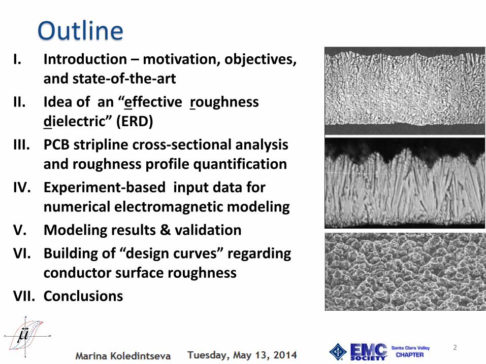
Outline I. Introduction – motivation, objectives,
and state-of-the-art
II. Idea of an “effective roughness dielectric” (ERD)
III. PCB stripline cross-sectional analysis and roughness profile quantification
IV. Experiment-based input data for numerical electromagnetic modeling
V. Modeling results & validation
VI. Building of “design curves” regarding conductor surface roughness
VII. Conclusions

3
3 Gbps 28 Gbps
• Conductor surface roughness lumps into laminate dielectric parameters.
• Any existing analytical and numerical models of conductor surface roughness are approximations.
• Study and adequate modeling of wideband behavior of dielectrics and conductors in PCBs is important from SI point of view.
VLP
• Conductor roughness affects both phase and loss constants in PCB transmission lines and results in eye diagram closure.
STD
HVLP
Motivation
The same dielectric, the same geometry, but different copper foil profiles
Low roughness - HVLP
Medium - VLP
High - STD
VLP
STD

4
Objectives • Develop a technique to accurately measure and extract laminate
dielectric parameters (DK=' & DF=tan) removing effects of conductors.
• Develop a physics-based model, which allows for simple incorporation of conductor surface roughness in electromagnetic numerical models of transmission lines.
• Test and validate the proposed model using measurements on a multitude of various test boards with different cross-sections and roughness profiles.
• Test and validate the proposed model using electromagnetic numerical simulations with different software tools.
• Develop a database for roughness parameters, corresponding to different types of copper foils used in PCBs.
5
A. Koul, M. Koledintseva, et al, Proc.
IEEE Symp. Electromag. Compat., Aug.
17-21, Austin, TX, 2009, 191-196
'2 "24. .cos2
r rc
'2 "24. .sin2
d r rc
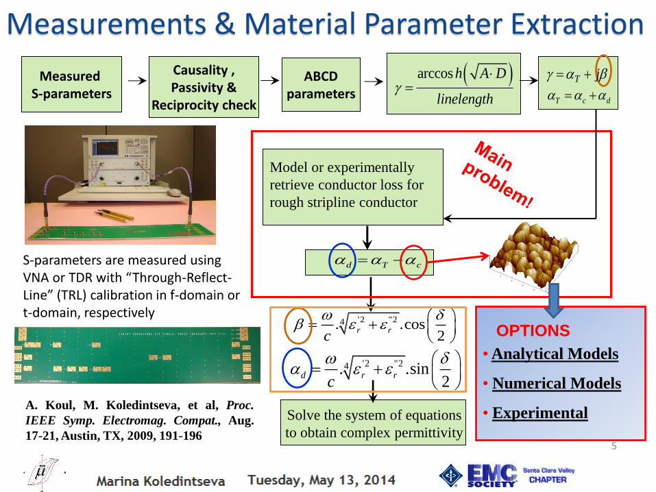
Measured S-parameters
Causality , Passivity &
Reciprocity check
ABCD parameters
T c d
arccos h A D
linelength
jT
Solve the system of equations
to obtain complex permittivity
d T c
Model or experimentally
retrieve conductor loss for
rough stripline conductor
OPTIONS
• Analytical Models
• Numerical Models
• Experimental
S-parameters are measured using VNA or TDR with “Through-Reflect-Line” (TRL) calibration in f-domain or t-domain, respectively
Measurements & Material Parameter Extraction

6
Existing Methods for Conductor Roughness Modeling
I. Correction coefficients for attenuation
• Periodic roughness models (Morgan, Sanderson, Sundstroem, Lukic)
• Hammerstad model (Hammerstad, Bekkadal, Jensen)
• “Snowball” model (Huray)
• Roughness hemispheres (Hall, Pytel)
• Stochastic models (Sanderson, Tsang, Braunisch)
II. Impedance boundary conditions
• Holloway, Kuester
III. Numerical electromagnetic modeling
• Deutsch
• Shlepnev
• X. Chen
IV. Experimental separation of conductor & dielectric loss
• Koledintseva et al
Stain-proof layer
Anti-tarnish layer
Drum foilDrum foil
Dendrite plating
Protective barrier
Stain-proof layer
Oxide treatment

7
• Experiment-based Differential and Extrapolation Roughness Measurement techniques (DERM and DERM-2) have been proposed to refine wideband DK and DF from roughness.
[1] A. Koul, M.Y. Koledintseva, S. Hinaga, and J.L. Drewniak, “Differential extrapolation method for separating dielectric and rough conductor losses in printed circuit boards”, IEEE Trans. Electromag. Compat., vol. 54, no. 2, Apr. 2012, pp. 421-433. [2] M.Y. Koledintseva, A.V. Rakov, A.I. Koledintsev, J.L. Drewniak, and S. Hinaga, “Improved experiment-based technique to characterize dielectric properties of printed circuit boards”, IEEE Trans. Electromag. Compat. (to be published soon in 2014)
• An Effective Roughness Dielectric (ERD) approach has been proposed to substitute inhomogeneous roughness boundary layer by a layer with homogenized dielectric properties.
[3] M.Y. Koledintseva, A. Razmadze, A. Gafarov, S. De, S. Hinaga, and J.L. Drewniak, “PCB conductor surface roughness as a layer with effective material parameters”, IEEE Symp. Electromag. Compat., Pittsburg, PA, 2012, pp. 138- 142.
Our Recently Published Works
8
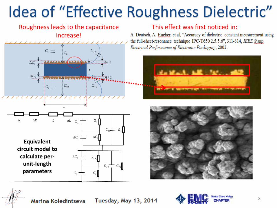
Idea of “Effective Roughness Dielectric”
8
1fG
R R1C
1C
1G
1G
2C
2C
2G
2G
1fC
2fC2fG
L L
Equivalent circuit model to
calculate per-unit-length parameters
Roughness leads to the capacitance increase!
1C
2C
w
01C
02C
1C
2C
t
/ 2A
/ 2A
1fC
2fC
This effect was first noticed in:

9
Tr
Ar t r
y
x
, 1(1 ) ( )
incl matrixeff y matrix incl
matrix incl y incl matrix
vv N
.matrix m mj 0
iincl i
j
2
1ln( )yN a
a
Maxwell Garnett Mixing Rule for aligned metallic inclusions
Depolarization factor of cylindrical inclusions
a=Ar/d Aspect ratio of inclusions
rA
d r
i rT Average peak-to-valley
roughness amplitude
Thickness of “roughness dielectric”
Intrinsic conductivity of “roughness inclusions”
Roughness quasi-period
Mixing Rule for “Effective Roughness Dielectric”

10
• HPF (high-performance foil) - 10 µm <Rz <15 µm
• STD (standard foil) – 5 µm <Rz<10 µm
• VLP (very-low profile foil) – 3 µm <Rz<6 µm
• RTF (reverse-treatment foil) – 3 µm <Rz<6 µm
• HVLP (hyper-very-low profile foil) – 1 µm <Rz<3 µm
• ULP (ultra-low roughness foil) – 0.5 µm < Rz < 1 µm
Various Types of Foils
Foils are mostly
isotropic in X and Z

11
1 2 3 4 5 1 2 3 4 5
5
p p p p p v v v v v
z
Y Y Y Y Y Y Y Y Y YR
Surface Profilometer
Roughness of conductors on PCB are
evaluated based on the amplitude data
only: Ra, Rq, Rz, and Rt.
• Mechanical
• Optical
Roughness data from board vendors
Foil / Trace Thickness t=12µm t=18µm t=35µm
Low rough (HVLP) 1.5 µm 1.5 µm 1.5 µm
Medium rough (VLP) 3 µm 3.5 µm 4 µm
Standard foil (STD) 5 µm 6 µm 8 µm
Standard Profilometer Roughness Evaluation
Problem: foil measured is not the same as “in situ”.

SEM & Oprical Cross-sectional Analysis of PCB Striplines
12
Cutting board for cross-sections
SEM
Optical

13
0 20 40 60 80 100 120 140 160 180-4
-3
-2
-1
0
1
2
3
4
1
2
34 56
7
1
2 3 4 5
67
8
Surface roughness profile image
x, m
y, m
0 20 40 60 80 100 120 140 160 180-1.5
-1
-0.5
0
0.5
1
1.5
2
1
2
3
4 5 6 7
8
9
10
11
12
1 2
3 4
5 6 7
8 910
1112
Surface roughness profile image
x, m
y, m
[S. Hinaga, S. De, A.Y. Gafarov, M.Y. Koledintseva, and J.L. Drewniak, “Determination of copper foil surface roughness from microsection photographs”, Techn. Conf. IPC Expo/APEX 2012, Las Vegas, Apr. 2012]. [S. De, A.Y. Gafarov, M.Y. Koledintseva, S. Hinaga, R.J. Stanley, and J.L. Drewniak, “Semi-automatic copper foil surface roughness detection from PCB microsection images”, IEEE Symp. EMC., Pittsburg, PA, 2012, pp. 132-137].
Conductor Roughness Profile Extraction
13

14
14
Roughness Characterization Flow Chart
1 2 3 4 5 6 7 8 91 2 3 4 5 6 7 9 8
SEM or optical image
Scale calculation
Object selection
Preprocessing noise removal
High boost filtering
Trace profile (foreground)
extraction
Trace side selection
Skin depth calculation &
morphological processing
Translation of pixel map to coordinate
data
Roughness profile coding & maxima/minima
searching
Non-linear de-trending
Removal of artifacts
Roughness quantification
(Ar, Λr, QR)
Image Processing Part
Computer Vision – Roughness Quantification Part

15
1 2 3 4
5 6 7 8 9 10 11
12
1 2 3 4 5 6 7
8 9 10 1112 13 14 15 16
Profile length L
Ar
-valley
-peak
Oxide side
Foil side
Average peak-to-valley amplitude:
Roughness quasi-period:
Roughness factor: r r
oxide foil
A AQR
peakvalley
peakvalley
NN
NLNL
2
valley
N
i
valleyi
peak
N
i
peaki
rN
Y
N
Y
A
valleypeak
1
1
Roughness Factor QR
Roughness Surface Generation from Statistical Analysis of Profile
16
Oxide Side
0
5
10
15
200
5
10
15
20
0.00
0.01
0.02
0.03
Foil Side
Rayleigh
=
2D PDF Generated Surfaces 3D PDF
0
2
4 0
2
4
0.0
0.2
0.4
Gauss
=

Finding Ar from PDF
17
Side STD VLP HVLP
Oxide Gaussian Gaussian Gaussian
Foil Rayleigh Rayleigh Gaussian
mean[pixel]
Blue line is measured from actual profile Red line is generated from PDF
𝐴𝑟 = 2 ∙ 𝑚𝑒𝑎𝑛 𝑝𝑖𝑥𝑒𝑙 ∙pixel’s value
𝑚𝑒𝑎𝑛 𝑖𝑠 𝐸 𝑥 = 𝑥∞
0
𝑓𝑥 𝑥 𝑑𝑥 𝐴𝑟 = 2 ∙ 𝐸 𝑥 ∙ 𝑝𝑖𝑥𝑒𝑙′𝑠 𝑣𝑎𝑙𝑢𝑒
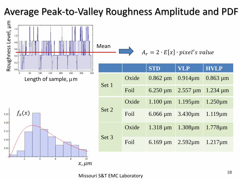
Mean
STD VLP HVLP
Set 1
Oxide 0.862 µm 0.914µm 0.863 µm
Foil 6.250 µm 2.557 µm 1.234 µm
Set 2
Oxide 1.100 µm 1.195µm 1.250µm
Foil 6.066 µm 3.430µm 1.119µm
Set 3
Oxide 1.318 µm 1.308µm 1.778µm
Foil 6.169 µm 2.592µm 1.217µm
Average Peak-to-Valley Roughness Amplitude and PDF R
ou
ghn
ess
Leve
l, µ
m
Length of sample, m
Missouri S&T EMC Laboratory 18
𝐴𝑟 = 2 ∙ 𝐸 𝑥 ∙ 𝑝𝑖𝑥𝑒𝑙′𝑠 𝑣𝑎𝑙𝑢𝑒
19
w1,
m
w2,m H, m P,
m
h1,
m
h2,
m
Ar1,
m
Ar2,
m
1,
m
2,
m
QR1 QR2 QR
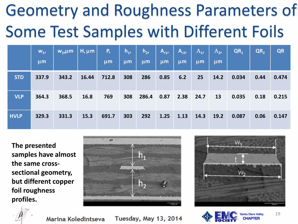
STD 337.9 343.2 16.44 712.8 308 286 0.85 6.2 25 14.2 0.034 0.44 0.474
VLP 364.3 368.5 16.8 769 308 286.4 0.87 2.38 24.7 13 0.035 0.18 0.215
HVLP 329.3 331.3 15.3 691.7 303 292 1.25 1.13 14.3 19.2 0.087 0.06 0.147
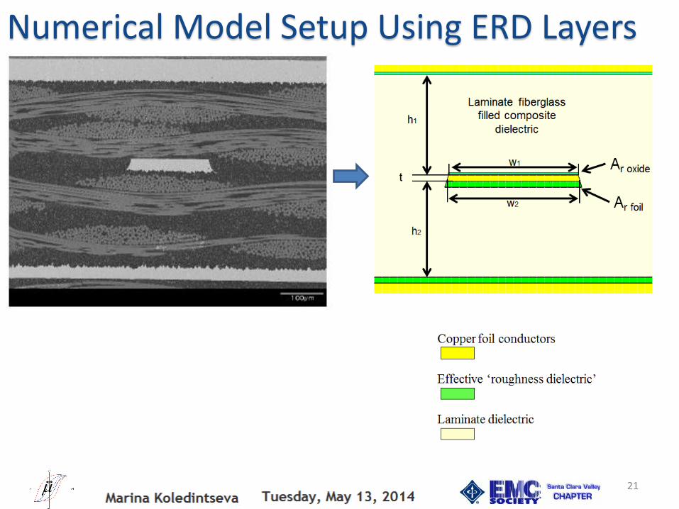
Geometry and Roughness Parameters of Some Test Samples with Different Foils
The presented samples have almost the same cross-sectional geometry, but different copper foil roughness profiles.
20
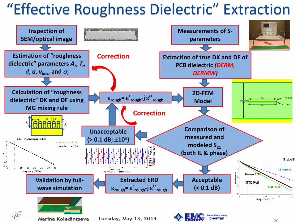
Inspection of SEM/optical image
Estimation of “roughness dielectric” parameters Ar, Tr,
d, a, vincl, and i
Calculation of “roughness dielectric” DK and DF using
MG mixing rule
2D-FEM Model
Measurements of S-parameters
Extraction of true DK and DF of PCB dielectric (DERM,
DERMW)
Comparison of measured and modeled S21
(both IL & phase)
Acceptable (< 0.1 dB)
Extracted ERD rough= rough-j rough
Unacceptable (> 0.1 dB; 10o)
rough= rough-j rough
Correction
Correction
rA
d
rT
“Effective Roughness Dielectric” Extraction
Validation by full-wave simulation
w1
w2
Tr oxide
Tr foil
21
Numerical Model Setup Using ERD Layers

22
0 5 10 15 200
100
200
300
400
500
600
700
800
900
d
, rad
/m
Frequency, GHz
extracted
-9
d =6.6*10 - 0.99*10
-22 2
0 2 4 6 8 10 12 14 16 18 200
0.5
1
1.5
2
2.5
3
3.5
4
4.5
5
Frequency (GHz)
T (
Np/
m)
High roughness -STD foil
Medium roughness - VLP foil
Low roughness - HVLP foil
Curve-fit data behaves as 2, &
2 2
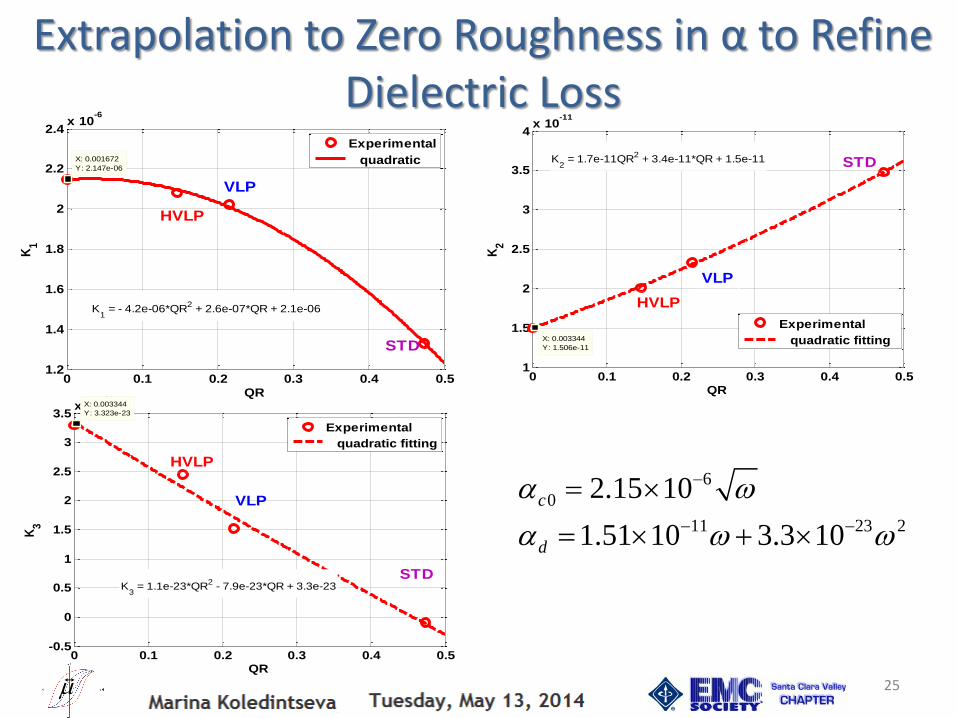
1 2 3 1 2 3T r r rK K K K K K
Smooth conductor loss
Dielectric loss
Loss due to conductor roughness
Curve-fit data behaves as 2, &
2 2
1 2 3 1 2 3T r r rB B B B B B
Due to skin depth in conductor
Due to propagation in the dielectric
Due to conductor roughness
T c d
T c d
Spectral Approach to Propagation Constant
23
0 5 10 15 20 25 30-30
-20
-10
0
Frequency, GHz
Ma
gn
itude
of
S 21,
dB
STD
VLP
HVL
0 5 10 15 20 25 30-80
-60
-40
-20
0
Frequency, GHz
Ma
gn
itu
de
of
S1
1,
dB
STD
VLP
HVL
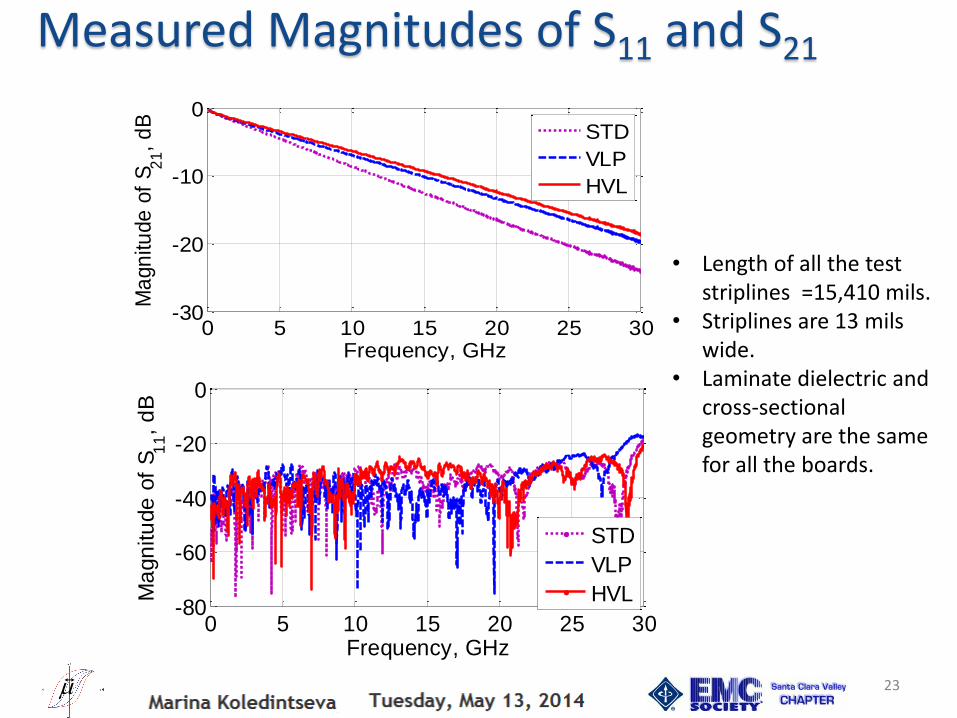
Measured Magnitudes of S11 and S21
• Length of all the test striplines =15,410 mils.
• Striplines are 13 mils wide.
• Laminate dielectric and cross-sectional geometry are the same for all the boards.
24
0 2 4 6 8 10-4
-2
0
2
4
Frequency, GHz
Phas
e S 21
, deg
rees
STD
VLP
HVLP
10 12 14 16 18 20-4
-2
0
2
4
Frequency, GHz
Phas
e S 21
, deg
rees
STD
VLP
HVLP
10 15 20 25 30-4
-2
0
2
4
Frequency, GHz
Pha
se S
21, d
egre
es
STD
VLP
HVLP
0 10 20 300
500
1000
Frequency, GHz
T,
rad/m
STD
VLP
HVLP
0 5 10 15 20 250
2
4
6
8
Frequency(GHz)
T,
Np/m
STD
VLP
HVLP
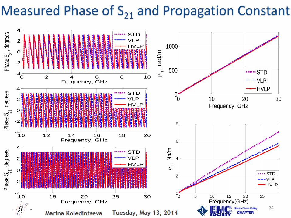
Measured Phase of S21 and Propagation Constant
25
0 0.1 0.2 0.3 0.4 0.51.2
1.4
1.6
1.8
2
2.2
2.4x 10
-6
K
1 = - 4.2e-06*QR
2 + 2.6e-07*QR + 2.1e-06
X: 0.001672
Y: 2.147e-06
QR
K1
Experimental
quadratic
HVLP
VLP
STD
0 0.1 0.2 0.3 0.4 0.51
1.5
2
2.5
3
3.5
4x 10
-11
K
2 = 1.7e-11QR
2 + 3.4e-11*QR + 1.5e-11
X: 0.003344
Y: 1.506e-11
QR
K2
Experimental
quadratic fitting
HVLP
VLP
STD
0 0.1 0.2 0.3 0.4 0.5-0.5
0
0.5
1
1.5
2
2.5
3
3.5x 10
-23
K
3 = 1.1e-23*QR
2 - 7.9e-23*QR + 3.3e-23
X: 0.003344
Y: 3.323e-23
QR
K3
Experimental
quadratic fitting
VLP
STD
HVLP
6
0
11 23 2
2.15 10
1.51 10 3.3 10
c
d
Extrapolation to Zero Roughness in α to Refine Dielectric Loss

26
Extrapolation to Zero Roughness in β to Refine Dielectric-Related Phase Constant
0 0.1 0.2 0.3 0.4 0.54.5
5
5.5
6
6.5
7
7.5
8
8.5x 10
-6
B
1 = 6.6e-06*QR
2 + 2.8e-06*QR + 5e-06
X: 0
Y: 4.966e-06
QR
B1
Experimental
quadratic fitting
HVLP
VLP
STD
0 0.1 0.2 0.3 0.4 0.5
6.36
6.38
6.4
6.42
6.44
6.46
6.48
6.5x 10
-9
B
2 = 2.2e-10*QR
2 + 1.6e-10*QR + 6.4e-09
X: 0
Y: 6.37e-09
QR
B2
Experimental
quadratic fitting
HVLP
VLP
STD
0 0.1 0.2 0.3 0.4 0.5-11.5
-11
-10.5
-10
-9.5
-9
-8.5
-8x 10
-23
B
3 = - 3.2e-23*QR
2 - 4.1e-23*QR- 8.2e-23X: 0.001672
Y: -8.194e-23
QR
B3
Experimental
quadratic fitting
HVLP
VLP
STD
6
9 23 2
5.0 10
6.37 10 0.82 10
c
d

27
0 0.1 0.2 0.3 0.4 0.50.5
1
1.5
2
2.5x 10
-6
QR
K1
BO
quadratic
CZ
quadratic
MB
quadratic
0 0.1 0.2 0.3 0.4 0.51
2
3
4
5
6
7x 10
-11
QR
K2
BO
quadratic
CZ
quadratic
MB
quadratic
0 0.1 0.2 0.3 0.4 0.5-4
-2
0
2
4x 10
-23
QR
K3
BO
quadratic
CZ
quadratic
MB
quadratic
6
0
11 23 2
2.15 10
1.5 10 3.0 10
c
d
Additional Procedure to Refine Dielectric Loss (with Two other Sets of Test Vehicles with Different Types of Foil)
1
1
1
2
2
2
3
3
3
This increases accuracy of extraction.

28
Additional Procedure to Refine Phase Constant (with Two other Types of Foil)
6
9 23 2
5.0 10
6.38 10 0.8 10
c
d
0 0.1 0.2 0.3 0.4 0.5-1.6
-1.4
-1.2
-1
-0.8x 10
-22
QR
B3
BO
quadratic
CZ
quadratic
MB
quadratic
1
2
3
0 0.1 0.2 0.3 0.4 0.5
5
6
7
8
9
10x 10
-6
QR
B1
BO
quadratic
CZ
quadratic
MB
quadratic
1
2
3
0 0.2 0.4 0.6 0.86.3
6.4
6.5
6.6
6.7
6.8
6.9x 10
-9
QR
B2
BO
quadratic
CZ
quadratic
MB
quadratic
1
2
3
This increases accuracy of extraction.

29
0 5 10 15 20 25 30 350
2
4
6
8
10
Frequency, GHz
, N
p/m
C0
D
T
11 23 21.51 10 3.3 10d
Extracted Loss in a Smooth Conductor (Roughness Parts are Removed)
smooth 0T C d
6
0 2.15 10c

30
The refined dielectric data (DK and DF) for all the test vehicles is used in
numerical electromagnetic modeling (2D-FEM)
Extracted Dielectric Properties of PCB Laminate Substrate
0 5 10 15 20 25 303.6565
3.657
3.6575
3.658
3.6585
Frequency, GHz
DK
Extracted DK for Megtron 6 "Old"
0 5 10 15 20 25 304.5
5
5.5
6
6.5x 10
-3
Frequency, GHz
DF
Extracted DF for Megtron 6 "Old"
Numerical model 1: Ansoft Q2D (2DFEM)
This model is used to extract
parameters of Effective Roughness
Dielectric (ERD): bright-green layers

31
Modeled & Measured S21 for Stripline with HVLP Foil (Q2D)

32
Modeled & Measured S21 for Stripline with VLP Foil (Q2D)

33
Modeled & Measured S21 for Stripline with STD Foil (Q2D)

34
The refined dielectric data (DK and DF) for all the test vehicles is used in
numerical electromagnetic modeling (2D-FEM)
Extracted Properties of Effective Roughness Dielectric
Foil Type
Tr1 (ox), µm
Tr2 (foil), µm
tanr (ox)
tanr (foil)
r (ox)
r (foil)
QR (ox)
QR (foil)
VR (ox), m
VR (foil), m
STD 1.7 12.4 0.01 0.17 5.0 12.0 0.034 0.44 0.085
25.30
VLP 1.74 4.76 0.02 0.13 5.1 9.0 0.035 0.18 0.178
7.42
HVLP 2.50 2.26 0.06 0.04
5.1 4.8 0.087 0.06 0.765 0.433
Set 1

35
Effective Roughness Dielectric Parameters as a Function of Roughness Factor

36
Effective Roughness Dielectric Parameters as a Function of Roughness Factor
Sets 1,2,3 – 13mil trace width Sets 4, 5 – 7 mil trace width
Region of Oxide Sides & HVLP
Region of Oxide Sides& HVLP
Region of VLP/RTF
Region of VLP/RTF
Region of VLP/RTF
Region of Oxide Sides & HVLP
Region of STD Region of STD
Region of STD

37
Numerical model 2: CST
Studio Suite 3D (Full-wave
FD MoM) – this model is
used for validation of the
extracted ERD data
Validation Using Full-wave Model (CST)
HVLP
VLP
STD
T. Vincent, M. Koledintseva, A. Ciccimancini, and S. Hinaga,
“Effective roughness dielectric in a PCB: measurement and full-
wave simulation verification”, IEEE Symp. EMC, Aug. 2014
(accepted)
38
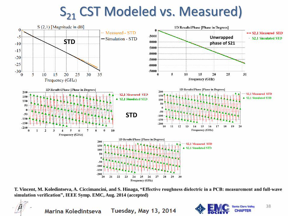
T. Vincent, M. Koledintseva, A. Ciccimancini, and S. Hinaga, “Effective roughness dielectric in a PCB: measurement and full-wave
simulation verification”, IEEE Symp. EMC, Aug. 2014 (accepted)
STD
Unwrapped phase of S21
S21 CST Modeled vs. Measured)
STD

39
0(1 )c c r 0
r
c
r
0r c c
Modeled & Measured Magnitude of S21 for Striplines with Different Foils
Slope of S21 as a function of frequency increases with the increase of surface roughness
0 5 10 15 20 25 30-25
-20
-15
-10
-5
0
Frequency, GHz
S2
1,
dB
Smooth conductor
STD
VLP
HVLP
21 08.686( )D csmoothS L
HVLP
STD
VLP
Smooth

40
0 0.1 0.2 0.3 0.4 0.50
0.1
0.2
0.3
0.4
QR
Ad
diti
ona
l slo
pe
R,
dB
/GH
z
Experimental points
linear
quadraticSTD
VLPHVLP
0 0.1 0.2 0.3 0.4 0.50
0.2
0.4
0.6
0.8
1
QR
Rn,
dB
/GH
z/m
Experimental points
linear
HVLP
VLP
STD
R=(S smooth- S rough)/f [dB/GHz] Rn=(S smooth- S rough)/f/L [dB/GHz/m]
Additional Slope in S21 as a Function of Roughness Factor

0 0.1 0.2 0.3 0.4 0.5-1
0
1
2
3
4
5
6
7x 10
-23
Q, m
K3~
2
SET I
SET II
QR, µm
0 0.05 0.1 0.15 0.2 0.25 0.3 0.35 0.4
3.6
3.7
3.8
3.9
4
4.1x 10
-6
Q, m
K1~
sq
rt(
)
Extrapolation to Zero Roughness
SET I
SET II
0 0.05 0.1 0.15 0.2 0.25 0.3 0.35 0.4
2
2.2
2.4
2.6
2.8
3
3.2
3.4
3.6
3.8
x 10-11
Q, m
K2~
Extrapolation to Zero Roughness
SET I
SET II
QR, µm QR, µm
41
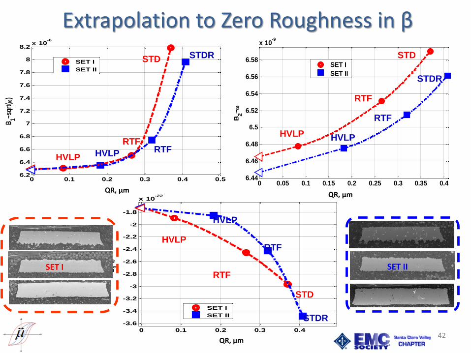
Extrapolation to Zero Roughness in α (7-mil Lines)
SET I
RTF
STD
HVLP
RTF
STD
HVLP
RTF
STD
HVLP RTF
STDR
STDR
HVLP RTF
RTF
SET II
41
HVLP
HVLP
STDR
0 0.1 0.2 0.3 0.4
-3.6
-3.4
-3.2
-3
-2.8
-2.6
-2.4
-2.2
-2
-1.8
x 10-22
Q, m
B3~
2
SET I
SET II
QR, µm 42
0 0.1 0.2 0.3 0.4 0.56.2
6.4
6.6
6.8
7
7.2
7.4
7.6
7.8
8
8.2x 10
-6
Q, m
B1~s
qrt(
)
SET I
SET II
0 0.05 0.1 0.15 0.2 0.25 0.3 0.35 0.46.44
6.46
6.48
6.5
6.52
6.54
6.56
6.58
x 10-9
Q, m
B2~
SET I
SET II
SET I SET II
HVLP
HVLP
HVLP
RTF
RTF
STD
STDR
RTF
HVLP
HVLP RTF
STD
STDR
STD
RTF
HVLP
STDR
RTF
QR, µm QR, µm
Extrapolation to Zero Roughness in β
43
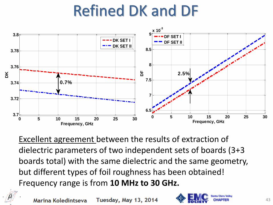
Refined DK and DF
0 5 10 15 20 25 303.7
3.72
3.74
3.76
3.78
3.8
Frequency, GHz
DK
DK SET I
DK SET II
0.7%
0 5 10 15 20 25 30
6.5
7
7.5
8
8.5
9x 10
-3
Frequency, GHz
DF
DF SET I
DF SET II
2.5%
Excellent agreement between the results of extraction of dielectric parameters of two independent sets of boards (3+3 boards total) with the same dielectric and the same geometry, but different types of foil roughness has been obtained! Frequency range is from 10 MHz to 30 GHz.

44
Dielectric Loss and Smooth & Rough Conductor Losses
0 5 10 15 20 25 300
1
2
3
4
5
6
d,
Np
/m
Frequency, GHz
SET I
SET II
0 5 10 15 20 25 300
0.5
1
1.5
c0,
Np
/m
Frequency, GHz
SET I
SET II
0 5 10 15 20 25 30-0.2
0
0.2
0.4
0.6
0.8
1
1.2
1.4
1.6
1.8
Frequency, GHz
ro
ug
h,
Np
/m
SET I STD
SET I RTF
SET I HVLP
SET II STDR
SET II RTF
SET II HVLP
SET II- STDR
SET I - STD
SET I - RTF
SET II - RTF
SET II - HVLP
SET I- HVLP
Total
conductor
loss
Smooth
conductor
loss
Rough conductor loss

Concentration of “roughness inclusions” decreases with distance from
zero-roughness plane
Maxwell Garnett mixing rule requires knowledge of volume concentration of
“roughness inclusions”. This volume concentration varies as a function of the
height y. Hence the dielectric properties homogenized by Maxwell-Garnett in each
incremental layer are also functions of y.
( ) 1 ( )(1 ( )) ( )
incl matrixMG matrix
matrix y incl matrix
y yy N
)(y
Effective Roughness Dielectric Approximation
Close to smooth conductor, y0=0
Deeper inside ambient dielectric, y1>y0
Deeper inside ambient dielectric, y2>y1
Closer to ambient dielectric, y3>y2
Ny is the depolarization
factor in y-direction.
and
45
d=Ar
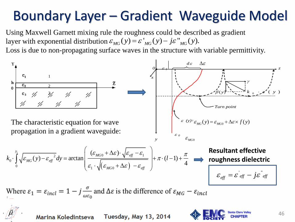
1
2
3
Using Maxwell Garnett mixing rule the roughness could be described as gradient
layer with exponential distribution
Loss is due to non-propagating surface waves in the structure with variable permittivity.
0 12
0
01 0
( )( ) arctan ( 1)
4
tyMG eff
MG eff
MG eff
k y dy l
( ) ' ( ) " ( ).MG MG MGy y j y
The characteristic equation for wave
propagation in a gradient waveguide:
effeffeff j '''
Boundary Layer – Gradient Waveguide Model
d
0 1 z
x
)(y )(0 yk
Turn point
(y)= 0 +d f(y)
0
y
0( ) ( )MG MGy f y
0MG
Resultant effective roughness dielectric
46

47
Set 1
STD 15 6.489 0.203 12.7
6.496 0.17 12.0 13 5.05 0.124 5.02
VLP 6 2.739 0.130 8.08
2.752 0.13 9.0 5 1.932 0.100 13.58
HVLP 2 1.083 0.048 5.01
1.086 0.04 4.8 1 0.158 0.203 44.76
Extracted from Gradient Model (on Foil Sides) Extracted from Q2D
Solution #
Turning point= Ar tanrough
𝜺′𝒓𝒐𝒖𝒈𝒉 𝒆𝒇𝒇 Ar tanrough 𝜺′𝒓𝒐𝒖𝒈𝒉 𝒆𝒇𝒇
Results for the Gradient Model: Set 1, Foil Side
There is a reasonable agreement; however, the results were obtained only for a limited number of samples.

Conclusions
48
• A new improved technique DERM2 to extract dielectric properties of a
laminate dielectric for a set of five test vehicles is demonstrated.
• A semi-automatic roughness profile extraction and quantification procedure
has been applied to SEM or optical microscopy pictures of microsections of
PCB stripline.
• A metric called “roughness factor” QR to quantify roughness profiles has
been introduced.
• The correlation between the additional slope in insertion loss due to
roughness and the roughness factor QR has been established. The effective
roughness dielectric layer concept was applied to numerically model (in 2D
FEM) all the five test vehicles.
• In the numerical models, the dielectric parameters of ambient dielectric
were taken as those obtained using the DERM2 procedure; the boundary
roughness layers were substituted by Effective Roughness Dielectric.
• This model and analysis lead to the development of the “design curves”
(additional slopes of insertion loss, or additional conductor loss as a
function of roughness parameter), which could be used by SI engineers in
their designs.

Acknowledgment
49
• I am very grateful to Scott Hinaga (Cisco) for collaboration, weekly discussions at
conference calls, support of ideas, and sponsoring this research in 2008-2014.
• I would like to thank graduate and undergraduate students of Missouri S&T who
contributed to this work: Amendra Koul (Cisco), Praveen Anmula (Mentor
Graphics), Soumya De (Cisco), Fan Zhou (Semtech), Aleksandr Gafarov (Mentor
Graphics), Aleksei Rakov (Moscow Power Engineering Institute), Oleg Kashurkin
(Missouri S&T), and Alexei Koledintsev (Missouri S&T).
• I would like to thank Prof. James Drewniak for an opportunity to work with EMC
Lab of Missouri S&T in 2000-2014, motivation for this research, and useful
discussions.
• I would like to thank Missouri S&T Materials Research Center colleagues – Dr.
Clarissa Wisner , Dr. Beth Culp, Prof. Matt O’Keefe, and Dr. Signo Reis (Saint
Gobain) for their help with SEM and optical micro photographs.
• This work was also partially supported by the National Science Foundation under
Grant No. 0855878 through NSF I/UCRC Program.

50
Thanks &


![PCB Report project [互換モード] - jms21.co.jp · Copper Clad Laminate Interlayer dielectric materials for HDI Electro plated copper foil ... Doosan LG Chem Panasonic ... PCB](https://img.pdfslide.us/doc/110x75/5b65638e7f8b9a2a5c8b7c70/pcb-report-project-jms21cojp-copper-clad-laminate-interlayer.jpg)