Embed Size (px)
Citation preview
1
Exploring the Pareto Front of Multi-ObjectiveSingle-Phase PFC Rectifier Design Optimization -
99.2% Efficiency vs. 7kW/dm3 Power DensityJ. W. Kolar, J. Biela and J. Minibock
ETH Zurich, Power Electronic Systems LaboratoryPhysikstrasse 3, CH-8092 Zurich, Switzerland
Email: [email protected]; www.pes.ee.ethz.ch
Abstract—Up to now, in the development of power electronicssystems, the reduction of the initial costs or the increase ofthe power density have been of primary concern. However,with increasing energy costs also the power conversion efficiencyis gaining higher and higher importance. Accordingly, whilemaintaining high power density, an efficiency as high as possiblemust be obtained.
In this paper the maximum attainable efficiency and thedependency of the efficiency limit on technological parametersis determined for single-phase PFC boost rectifiers. In a firststep basic PFC boost rectifier topologies are briefly comparedwith regard to high efficiency and a dual-boost PFC rectifierwith integral common-mode filtering is selected as basis for theinvestigations. Next, simple approximations of the technologicallimits of the system performance are calculated in the efficiency-power density plane. With this, the Feasible Performance Spaceand the reduction in power density which has to be acceptedfor increasing the efficiency are clarified, and the trade-off limitcurve (Pareto Front) of a multi-objective, i.e. efficiency and powerdensity design optimization is determined. Furthermore, a com-prehensive numerical efficiency optimization is carried out whichidentifies an efficiency limit of 99.2% for a 3.2kW system. Thetheoretical considerations are verified by experimental resultsfrom a laboratory prototype of the ultra-high efficiency systemachieving 99.1% efficiency at a power density of 1.1kW/dm3,as well as those from an ultra-compact dual-boost PFC rectifier(95.8%, 5.5kW/dm3) and a very low switching frequency (3kHz)conventional PFC boost rectifier (96.7%, 2kW/dm3). Finally, thesensitivity of the efficiency optimum with regard to varioustechnological parameters is analyzed and an outlook on thefurther course of the research is given.
I. INTRODUCTION
At present 40% of the total worldwide energy use isbased on electricity generation, whereby the mean conversionefficiency of fossil energy into electrical energy is only around35% [1]. By 2030 an increase in electricity use by 50% isforecast, whereas the generation efficiency will only increaseto 38%. A large fraction of this energy will subsequently beconverted and conditioned by power electronics systems. Thus,in view of the low generation efficiency, the energy efficiencyof the power electronics converters will gain eminent impor-tance in the conservation of resources.
Up to now, in the development of power electronics systems,reduction of the initial costs or increase of power density havebeen of primary concern [2]–[5]. Efficiency increase was only
Future
Failure Rate
Volume
State-of-the-artWeightLosses
Costs
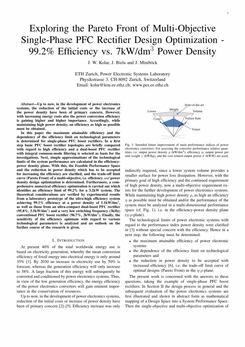
Fig. 1: Intended future improvement of main performance indices of powerelectronics converters. For assessing the converter performance relative quan-tities, i.e. output power density ρ (kW/dm3), efficiency η, output power perunit weight γ (kW/kg), and the cost related output power σ (kW/e) are used.
indirectly required, since a lower system volume provides asmaller surface for power loss dissipation. However, with theprimary goal of high efficiency and the continued requirementof high power density, now a multi-objective requirement ex-ists for the further development of power electronics systems.While maintaining high power density ρ, as high an efficiencyη as possible must be obtained and/or the performance of thesystem must be analyzed in a multi-dimensional performancespace (cf. Fig. 1), i.e. in the efficiency-power density plane(η-ρ-plane).
The technological limits of power electronic systems withregard to the performance index power density were clarifiedin [3] without special concern with the efficiency. Hence in anext step, the following must be determined:• the maximum attainable efficiency of power electronic
systems• the dependence of the efficiency limit on technological
parameters and• the reduction in power density to be accepted with
increased efficiency [6], i.e. the trade-off limit curve ofoptimal designs (Pareto Front) in the η-ρ-plane.
The present work is concerned with the answers to thesequestions, taking the example of single-phase PFC boostrectifiers. In Section II the design process in general and thesubsequent evaluation of the power electronics systems arefirst illustrated and shown in abstract form as mathematicalmapping of a Design Space into a System Performance Space.Then the single-objective and multi-objective optimization of

2
this mapping are discussed.In Section III topologies of PFC boost rectifier systems
are briefly compared with regard to high efficiency, and adual-boost PFC rectifier with integral common-mode (CM)filtering is selected as the basis for further investigations.In Section IV simple approximations of the technologicallimits of the system performance are calculated in the η-ρ-plane, i.e. the Feasible Performance Space is determined. Nexta comprehensive optimization is carried out with regard toefficiency (Section V).
Then in Section VI experimental results from a laboratorysample of the ultra-high efficiency system are shown as wellas those from an ultra-compact dual-boost PFC rectifier and alow-frequency conventional PFC boost rectifier. In Section VIIthe prediction of the Pareto Front of a simultaneous efficiencyand power density optimization of the system is discussed. Fi-nally, in Section VIII the sensitivity of the efficiency optimumwith regard to various technological parameters is analyzedand in Section IX an outlook on the further course of theresearch is given.
II. MULTI-OBJECTIVE OPTIMIZATION OF POWERELECTRONIC CONVERTER PERFORMANCE
The essential steps in the design process and the subse-quent evaluation of a power electronic system based uponperformance indices are shown in Fig. 2 in simplified graphicform. Fundamentally, a circuit topology and an associated
Materials
Components
System
• Semiconductor Mat .• Conductor Mat.• Magnetic Mat .• Dielectric Mat .• etc.
• Doping Profiles• Geometric Properties• Winding Arrangements• Magnetic Core Geometries• etc.
• Specifications• Operation Limits• Converter Topology• Modulation Scheme• Control Concept• Operation Mode• Operating Frequ.• etc.
• Power Semiconductor• Interconnections• Inductors, Transf.• Capacitors• Control Circuit• etc.
• Evaluation Formulas• Lifetime Models• Cost Models• etc.
• Phase-Shift DC/DC Conv.• Resonant DC/DC Conv.• DC Link AC/AC Conv.• Matrix AC/AC Conv.• etc.
Performance Space• Efficiency• Power Density• Costs• Reliability• etc.
η
ρ
Costs ( ),f x k
2m
1m
Fig. 2: Abstracted graphical representation of the design and assembling ofa power electronics converter as transition m1 from materials to componentsand subsequently from components to the required system (transition m2).The assessment of the design quality is by performance indices and/orin a Performance Space (mapping f(~x,~k), (4)).The transitions m1 andm2 are defined by parameter values and/or values of design variables xnwhich are selected in the course of the design considering the requiredsystem specifications and minimum performance requirements, i.e. equalityand inequality constraints. Furthermore, design constants kl and limits ofthe employed materials are taking influence on m1 and m2. Overall, thedesign process and the design evaluation can be described as a mapping of amulti-dimensional Design Space with coordinate axis xn and kl into a multi-dimensional Performance Space which is defined by the performance indicespi (Fig. 5).
modulation and control process must be selected and thecomponent values and control parameters, etc., determinedin such a way that system specifications and regulations arefulfilled. The system must hence, e.g., deliver in a definedrange of input voltage the required output power, the switchingfrequency ripple of the output voltage must be limited to anupper limit, the correction of the output voltage after a loadstep must take place in a defined maximum time and theregulations regarding EMI emission must be complied with.Furthermore, typical minimum requirements regarding systemperformance, e.g. regarding the costs or the efficiency mustbe fulfilled. Selection of the components must be done insuch a way that material limits, such as the maximum junctiontemperature of the power semiconductors or a maximum fluxdensity swing of magnetic material or the maximum currentloading of a filter capacitor are complied with.
The components are realized starting from a material base,i.e. semiconducting and conducting materials, magnetic mate-rials, dielectrics and insulating materials, etc., whereby a mul-titude of design variables is to be specified. E.g., with regard tomagnetic components, a core material must be selected and thecore geometry, winding arrangement, winding cross-sectionand also the realization of the winding with stranded wire,round wire or a copper foil, etc. specified. Other components,e.g. power semiconductors or semiconductor modules can nolonger be influenced in the design, but are available fromsemiconductor manufacturers in prefabricated form for variousapplication areas (e.g. components with low on-state voltagebut higher switching losses). The design is thus limited to theselection of a suitable component.
Overall this means a large number of design variables anddesign constants, which must be specified in the course ofdimensioning in such a way that the system specificationsare fulfilled and a target performance attained. Hence from amathematical viewpoint, in a multi-dimensional Design Space,
ρ ρAm
BB*
A
fPfPm
Fig. 3: Optimization of the power density ρ of a converter (single-objectiveoptimization) by optimal selection of the switching frequency fP and furtherdesign variables xn (not shown). Based on a mathematical description of themapping of the Design Space into the Performance Space, the performanceof different converter topologies (A or B) or the influence of changing theoperation mode (B or B∗) can be shown in direct dependency of fP or xnand an optimum parameter value fPm can be selected.

3
100%
0%ρ kW
η
ρAmρA,
ηA,
ρη
ηA,
ρA,
ηA
ρA
dm3[ ]fP
fp,
fP,
C
C ,,
,C
Pareto FrontII
I
b)a)
Fig. 4: Representation of the power density optimization (single-objectiveoptimization, cf. a)) of a system concept A according to Fig. 3 in thepower density / efficiency plane (η-ρ-plane, cf. b)). In case the efficiencyis included into the optimization, a whole set of solutions results, accordingto the different weightings wi of the objectives (cf. (7)). The best possible,i.e. Pareto-optimal solutions of this multi-objective optimization are definingthe Pareto Front. For solutions along the Pareto Front the improvement of theefficiency in any case results in a reduction of the realizable power densityρ. A design C therefore is not Pareto-optimal, as solutions C′ and C′′ existwhich show a high power density at the same efficiency (cf. C′) or a higherefficiency at same power density (cf. C′′). The end points I and II of the ParetoFront are defined by the results of single-objective optimizations concerningpower density or efficiency.
in which each design variable
~x = (x1, x2, . . . xn) (1)
or design constant
~k = (k1, k2, . . . kl) (2)
is assigned a coordinate axis, a design vector must be specifiedsuch that the side conditions defined by system specificationsor a minimum performance requirement
~r = (r1, r2, . . . rm) (3)
are fulfilled [7], [8]. Here also the circuit topology, modulationand control processes, etc. can be seen as design variables.
Typically there are considerably more design variables thanside conditions, so that a large number of different designs ispossible. Within the scope of an optimization, this multitudeof solutions can be limited to one optimal design, which e.g.maximizes a system performance index defined as qualitycriterion
f(~x,~k)→ Max, (4)
whereby one has to consider as side conditions functions
gi
(~x,~k, ~r
)= 0 i = 1, 2, . . . p (5)
hj
(~x,~k, ~r
)≥ 0 j = 1, 2, . . . q (6)
which describe the inner converter function and the systemrequirements or specifications, and minimum values of otherPerformance Indices [7]. If for example the efficiency ischosen as the quality criterion, the calculation of f
(~x,~k)
inthe course of the optimization the sum of the losses
∑PV i
of a design must be determined and therefrom the efficiencycalculated according to η = 1−
∑PV i/PO (where PO is the
output power).
Referred to Fig.2 the transitions m1 and m2 are defined byspecifying the design variables. By optimizing a performanceindex and subsequent calculation of all other performanceindices a point in the multi-dimensional Performance Spaceis then assigned to the system thus formed. Hence overall theDesign Space is mapped into the Performance Space, or aperformance vector is assigned to a design vector.
In order to simplify the optimization (4), in the field ofpower electronics the switching frequency fP , which influ-ences a large number of internal characteristics of a design(e.g. the cross-section of the magnetic core of a transformerand its core and winding losses, as well as the switching lossesof the power semiconductors) and is in non-linear dependenceon these characteristics, is often selected as an explicit param-eter. As shown in Fig. 3 with the example of a power densityoptimization, the optimization can then be represented clearlyor the sensitivity of the optimum with regard to fP be directlystated. Furthermore, the topology is typically not an elementof the Design Space, but the optimization is analyzed on thebasis of different circuit structures (A or B), or for a definedbasic circuit structure and various operating modes (B andB∗, e.g. hard or soft switching, or operation in continuous ordiscontinuous conduction mode).
As mentioned in the introduction, however, in future severalquality criteria will have to be fulfilled simultaneously for adesign (multi-objective design), so that∑
wifi
(~x,~k)→ Max;
∑wi = 1 (7)
results as a mathematical requirement. The weightings ofthe individual criteria determine the compromise between theindividual optimization goals, e.g. between power density andefficiency. Overall, then, there results not a single best solutionbut a set of solutions (cf. Fig. 4), i.e. a Pareto Front in thePerformance Space [9], [10] (connection I-II in Fig. 4). Forpoints of the Pareto Front an increase in the efficiency isonly possible with a decrease in the power density (increaseof weighting wη and decrease of wρ), i.e. the design is forthe chosen parameters wη and wρ the best possible and nodesign exists that would offer the same power density at higherefficiency. A design with performance C is in this sense notPareto-optimal, since it is dominated both by a design C ′ orby a design C ′′ (cf. Fig. 4).
It is now interesting to analyze the result of a single-objective power density optimization in the η-ρ-PerformanceSpace. Corresponding to a weighting wη = 1, wρ = 0, withoptimal switching frequency fPm (cf. Fig. 3) the point I ofthe Pareto Front is reached; for other values of the switchingfrequency a non-Pareto-optimal performance exists.
To summarize, then, to determine the best possible com-promise between the efficiency and the power density, thedesign of power electronics systems must be represented asa mathematical mapping f
(~x,~k)
of the Design Space intothe Performance Space with corresponding side conditions giand hj (cf. Fig. 5) and the Pareto Front for various circuittopologies A, B or modulation processes or operating modesB, B∗ etc. determined. In this way the best possible conceptcan be chosen for a required target performance (η, ρ), or via
4
ρ
ηx1
x2
kk *
Design Space
ρAm
BB*
A
Performance Spacek1
k2
δk p
p*
δp
Fig. 5: Abstraction of the multi-objective design of a power electronicsconverter as mapping of a multi-dimensional Design Space (or ParameterSpace, shown for two dimensions) into a multi-dimensional PerformanceSpace (shown for two dimensions). Performing a multi-objective optimizationidentifies the Pareto Front which allows an immediate and comprehensivecomparison of converter concepts and/or the selection of the concept best fit-ting given performance requirements. Furthermore, based on the mathematicaldescription of the mapping of the Design Space into the Performance Spacethe sensitivity d~p/d~k of the system performance concerning an improvementd~k of the technology basis and/or an increase of the limit values of designconstants could be directly analyzed. This facilitates a systematic roadmappingof technologies.
comparison of the performance of industrial systems with thetheoretically best possible concept, a technology evaluationcarried out. Furthermore, the influence of further technologicaldevelopments δ~k in the material or technology base may besimply estimated, since the mathematical analysis/optimizationshows directly the resulting gain δ~p in system performance.Thus, the optimization can also be employed in the reverse di-rection to determine the most effective change in a technology,i.e. serve as the basis for a technology roadmapping process.
In the following, the η-ρ-Pareto Front for single-phase PFCboost rectifiers is analyzed. There, in order to reduce thecomputing effort, the Pareto Front is not calculated directly,but an efficiency maximization is performed and then the η-ρ-Pareto Front approximated analytically. The dependenciesof the Pareto Front on technological parameters then becomedirectly clear.
III. SELECTION OF A HIGH-EFFICIENCY SINGLE-PHASEPFC TOPOLOGY
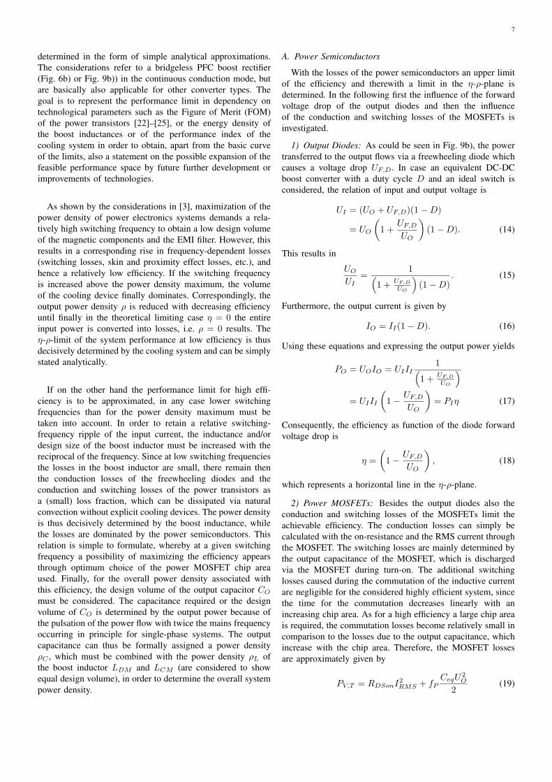
The basis of efficiency optimization is the choice of asuitable circuit topology that enables minimal semiconductorlosses to be attained with low semiconductor expense andhence low realization costs. The basic concepts of single-phasePFC boost rectifiers are shown in Fig. 6. As also describedin [11], with regard to low conduction losses, preferably abridgeless PFC boost rectifier (or dual-boost PFC rectifier, cf.Fig. 6b)) should be selected, since then with keeping S2 con-tinuously in the on-state for uN > 0 (and/or S1 for uN < 0)in the turn-on interval, only two MOSFET on-resistances andin the turn-off and/or boost interval only one diode and onepower MOSFET lie in the current path. SiC Schottky diodesare preferably used here as freewheeling diodes with regardto low switching losses. The use of relatively complex soft-switching topologies [12], [13] can thus be avoided and ishence not further discussed here. If for a conventional boostPFC rectifier (Fig. 6a)) equally low conduction losses were
RL
UO
uN
L
CO
RL
D1 D2
D3
D5
S1
D4
LD1 D2
S2S1
LD1 D2
D3 D4
UO
CO
UO
CO
RL
S2
S1
+
+
+
uN
uN
a)
b)
c)
Fig. 6: Basic topologies of single-phase power factor corrected (PFC) boost-type rectifier systems; a) conventional PFC boost rectifier, b) bridgeless ordual-boost PFC rectifier, c) dual-boost AC-switch PFC rectifier.
to be attained in the turn-on and boost state, four powerMOSFETs, i.e. a synchronous rectification would have to beused instead of the diodes D1−D4 of the input rectifier bridge,i.e. in total a MOSFET chip area of 9 AChip (AChip is thechip area of a single boost transistor of Fig. 6b)), as wellas one SiC freewheeling diode. As a further alternative forthe dual-boost AC-switch PFC rectifier (Fig. 6c), [14]), thediodes of one bridge leg, e.g. D2 and D4 could be replaced bypower MOSFETs and D1 and D3 realized as SiC diodes [11].In summary, with regard to the chip area or semiconductorrequirements (Fig. 7), the bridgeless PFC boost rectifier isclearly preferable when high efficiency is demanded.
However, a switching frequency common-mode (CM) volt-age occurs at the output for the system depicted in Fig. 6b), incontrast to the circuits shown in Figs. 6a) and c), where onerail of the output voltage bus is always connected to a mainsvoltage terminal via a diode or in the case of the synchronousrectification described above, via a power MOSFET. If theboost inductance is divided to the two AC input lines with theaim of lowering the conducted interference emission [15], thecommon-mode voltage uCMn of the negative output voltagebus n shows the time behavior depicted in Fig. 8. From simpleconsideration,
uCMn =12uN for S = on (8)
uCMn =12
(uN − UO) for S = off (9)
applies independent of the polarity of the mains voltage.

5
Considering the duty cycle of the switching power transistorS
d = 1− uNUO
, (10)
there then follows the local mean value uCMn of uCMn
referred to a pulse period
uN ≥ 0 uCMn = 0 (11)uN < 0 uCMn = uN . (12)
According to [16], a switching frequency variation of theoutput CM voltage can be suppressed by two return and/orclamping diodes (Fig. 9a)); there then exists a coupling ofmains and output comparable to the circuit in Fig. 6a) orFig. 6c). As described in [17], the boost inductance shouldbe preferably implemented as shown in Fig. 9a) to minimizethe design volume. LDM1 and LDM2 are realized here withmagnetic cores of the same type and the same number of turns.Because of the inverse coupling of the windings and the seriesconnection of LDM1 and LDM2, the voltages coupled to thenon-current carrying side then cancel each other out, i.e. noshort circuit of the sum voltage occurs over S1 and D3 or S2
and D4. Then, contrary to a magnetically separated realizationof the inductors, always the series connection of LDM1 andLDM2 is effective, which enables approximately a halving ofthe core volume [17]. However, in order to obtain the samelow conductive losses as for the circuit in Fig. 6b), the diodesD3 and D4 would have to be replaced again by synchronousrectifiers, so that overall a chip area requirement of 4AChipwould result (Fig. 7).
It is therefore obvious to consider alternative possibilities ofsuppressing the output CM voltage of the circuit depicted inFig. 6b). Here it is of advantage to employ a CM filter conceptknown from three-phase PWM rectifier systems [18], [19],for which the output in principle also exhibits a switching-frequency CM voltage. The resulting circuit of the dual-boostPFC rectifier with integral CM filter is shown in Fig. 9b).Instead of the clamping diodes, CM filter capacitors CCM1
No. of DiodesMOSFET Area
9
7
6
8
5
4
1
0
3
2
Conventional
Dua
l-Boo
stC
lam
ping
Dio
des
Dua
l-Boo
stA
C-S
witc
h
Dua
l-Boo
stIn
tegr
. CM
Fitl
er
Con
vent
iona
l
Dua
l-Boo
stC
lam
ping
Dio
des
Dua
l-Boo
stA
C-S
witc
h
Dua
l-Boo
stIn
tegr
. CM
Fitl
er
Fig. 7: Total MOSFET chip area required for equal conduction losses of theconverter topologies shown in Fig. 6a) and c) and Fig. 9a) and b). Furthermoreshown: Quantity of required fast recovery (SiC) freewheeling diodes. For thetopology Figs. 6a) the diodes D1-D4, and for Figs. 6c) diodes D2 and D4 arereplaced by power MOSFETs. The same is true for D3 and D4 in Fig. 9a).
0 2 4 6 8 10 12 14 16 18 20
-200
-100
100
200
-400
-300
Time [ms]
Vol
tage
[V]
0 uCMn
uCMn
Fig. 8: Common-mode (CM) voltage uCMn of the dual-boost PFC (measuredfrom the negative output voltage rail n towards earth) for a symmetricpartitioning of the boost inductor to the AC lines; uCMn denotes the localaverage value of uCMn related to a pulse period TP = 1/fP .
D1 D2
S2S1
UO
CO
RL+
LDM2LDM1
D3 D4
D1 D2
S2S1
UO
CO
RL+
LCMLDM
CCM2CCM1
CDM
uN
uN
a)
b)
p
n
p
n
Fig. 9: Circuit measures for avoiding a high-frequency CM voltage of theoutput of a dual-boost PFC rectifier; a) clamping diodes; b) capacitivecoupling of the output voltage to the mains and/or earth. The inverse magneticcoupling of the partial windings of LDM1 and LDM2 in a) allows tosimultaneously utilize both inductors for each input current direction; the totalvoltage appearing across the partial windings not participating in the currentconduction is equal to zero, accordingly diode D3 or D4 is not forced intoconduction. As always only one partial winding of LDM1 and LDM2 isconducting current, LDM1 in contrast to LCM of b) does not act as a CMinductor.
and CCM2 are employed here for high-frequency connectionof the output to the mains. The switching-frequency part ofthe CM voltage uCMn is then absorbed by a CM inductanceLCM . The dimensioning of LCM can simply be consideredvia a CM equivalent circuit diagram of the system [11] andthe associated time behavior of switching-frequency common-mode voltage 1/2uS∼ with uS∼ = uS−uS) (Fig. 10); here uSis the voltage occurring across the switching power transistor,e.g. across S1 for uN > 0.
For the interference sources effective between n and earth

6
uN
LCM
CCM
uS uS~
CEq
12
12
12 uS
,uS~,
I
0 2 4 6 8 10 12 14 16 18 20-200
-100
100
200
300
400
Time [ms]
Vol
tage
[V]
0
us~12
a)
b)
n
Fig. 10: CM-equivalent circuit of the converter shown in Fig. 9b) (CCM =CCM1 +CCM2) and time behavior of the switching frequency CM voltage1/2uS∼ of the negative output voltage rail n. 1/2uS∼ is low-pass filtered byLCM and CCM providing typ. about 60dB attenuation. Assuming an idealmagnetic coupling of the partial windings the boost inductor LDM is notactive for CM filtering Due to the earth connection of one mains terminal theAC side CM voltage is defined by half the mains voltage. After capacitivecoupling of n to the mains and/or earth via CCM only the drain voltage uS(related to n) of the switching power MOSFET is remaining as high frequencynoise source which can be translated into an equivalent noise source u′S=u′S+ u′S∼ and an equivalent coupling capacitance CEq considering the parasiticearth capacitances Cp + Cn of the positive and negative output voltage railsp and n.
follows
u′S =CSCEq
uS u′S∼ =CSCEq
uS∼ (13)
with
CEq = 2CS + Cp + Cn
(CS is the parasitic capacitance between the drain of a powerMOSFET and earth, Cp and Cn are the earth capacitances ofthe positive and negative output voltage rail, p and n ).
The common-mode inductance LCM and the equivalentcapacitance CCM = CCM1 +CCM2 (CCM1 = CCM2) act aslow-pass filters for the CM voltage 1/2uS = 1/2(uS + uS∼),whereby the low-frequency part 1/2uS , with correspondingdimensioning, is absorbed to a large extent by CCM and hencecauses only a relatively low flux density swing of LCM . Themagnetic dimensioning of LCM thus has only to be performedfor a switching-frequency voltage of maximum ±UO/4 with50% duty cycle (Fig. 10). As a concrete dimensioning andexperimental verification shows (Chapter V), there results atypical design volume of LCM comparable with the boostinductance LDM .
However, through CCM , as also through the diodes D3
or D4 (Fig. 9a)), the CM interference emission throughthe parasitic drain capacitance CS of the switching powertransistor switching, represented in Fig. 10a) by the equivalent
interference voltage u′S = u′S + u′S∼ and CEq , is fed directlyto the mains. Accordingly, in order to comply with the radiodisturbance regulations of CISPR 22 Class B, a further CMfilter stage must be placed on the mains side next to LCM andCCM or D3 and D4 (Position I in Fig. 10a)).
Note: For a dual-boost converter structure with magneticallyisolated inductances in both AC input lines, a balancing ofthe CM interference emission could be employed as shownin Fig. 14 of [20] because of the phase opposition of theCM voltages of the drains of the power MOSFETs S1 andS2 (cf. Fig. 13 in [19]) instead of D3 and D4 or CCM .However, a switching-frequency CM voltage of the output thenstill occurs; furthermore, the balancing is influenced by theearth capacitance of the load connected to the output. For thisreason, this concept is not be pursued further here.
In summary, the circuit in Fig. 9b) exhibits clear advantagesover that in Fig. 9a) with regard to the total semiconductor arearequired for specified conduction and switching losses. If LCMand LDM are implemented with the same magnetic cores asLDM1 and LDM2 in Fig. 9a), i.e. only one magnetic coreused for LDM , the effective boost inductance is halved or thedifferential mode ripple increases by a factor of 2. As a result,a 6dB higher DM interference level is to be expected which,however, can be relatively simply lowered by increasing thecapacitance of the DM filter capacitor CDM . By use of thesecond magnetic core for the realization of LCM , the CMinterference level is reduced to a value comparable to Fig. 9a).With regard to electromagnetic compatibility both conceptsare thus to be regarded as equal. Accordingly, for furtherconsiderations, Fig. 9b) is chosen as basis. For the systemspecifications we set:
TABLE I: Specifications of the considered single phase PFC rectifiers.
Output power PO 3.2kWLine voltage UN 230±10%
Output voltage UO 365VAmbient Temperature 45C
There, two parallel subsystems each with 1.6kW outputpower are employed in order to be able to switch off onesystem in the partial load region and thus assure a highefficiency over as wide a load range as possible.
In connection with efficiency maximization it is importantto point out that the freewheeling diodes of the dual-boosttopology cannot be complemented by synchronous rectifiers,i.e a super-junction MOSFET with antiserial low voltageMOSFET. This is because the power MOSFET working as asynchronous rectifier would represent a temporary short circuitwhen switching on the boost transistor again, because of thehigh output capacitance at low voltage, and thus lead to amassive increase in switching losses.
IV. ANALYTICAL APPROXIMATION OF η-ρ-PERFORMANCELIMITS
In the following, before numerical optimization (ChapterV), the limit of the system performance attainable in theη-ρ-plane, i.e. the Feasible Performance Space [21] will be
7
determined in the form of simple analytical approximations.The considerations refer to a bridgeless PFC boost rectifier(Fig. 6b) or Fig. 9b)) in the continuous conduction mode, butare basically also applicable for other converter types. Thegoal is to represent the performance limit in dependency ontechnological parameters such as the Figure of Merit (FOM)of the power transistors [22]–[25], or the energy density ofthe boost inductances or of the performance index of thecooling system in order to obtain, apart from the basic curveof the limits, also a statement on the possible expansion of thefeasible performance space by future further development orimprovements of technologies.
As shown by the considerations in [3], maximization of thepower density of power electronics systems demands a rela-tively high switching frequency to obtain a low design volumeof the magnetic components and the EMI filter. However, thisresults in a corresponding rise in frequency-dependent losses(switching losses, skin and proximity effect losses, etc.), andhence a relatively low efficiency. If the switching frequencyis increased above the power density maximum, the volumeof the cooling device finally dominates. Correspondingly, theoutput power density ρ is reduced with decreasing efficiencyuntil finally in the theoretical limiting case η = 0 the entireinput power is converted into losses, i.e. ρ = 0 results. Theη-ρ-limit of the system performance at low efficiency is thusdecisively determined by the cooling system and can be simplystated analytically.
If on the other hand the performance limit for high effi-ciency is to be approximated, in any case lower switchingfrequencies than for the power density maximum must betaken into account. In order to retain a relative switching-frequency ripple of the input current, the inductance and/ordesign size of the boost inductor must be increased with thereciprocal of the frequency. Since at low switching frequenciesthe losses in the boost inductor are small, there remain thenthe conduction losses of the freewheeling diodes and theconduction and switching losses of the power transistors asa (small) loss fraction, which can be dissipated via naturalconvection without explicit cooling devices. The power densityis thus decisively determined by the boost inductance, whilethe losses are dominated by the power semiconductors. Thisrelation is simple to formulate, whereby at a given switchingfrequency a possibility of maximizing the efficiency appearsthrough optimum choice of the power MOSFET chip areaused. Finally, for the overall power density associated withthis efficiency, the design volume of the output capacitor COmust be considered. The capacitance required or the designvolume of CO is determined by the output power because ofthe pulsation of the power flow with twice the mains frequencyoccurring in principle for single-phase systems. The outputcapacitance can thus be formally assigned a power densityρC , which must be combined with the power density ρL ofthe boost inductor LDM and LCM (are considered to showequal design volume), in order to determine the overall systempower density.
A. Power Semiconductors
With the losses of the power semiconductors an upper limitof the efficiency and therewith a limit in the η-ρ-plane isdetermined. In the following first the influence of the forwardvoltage drop of the output diodes and then the influenceof the conduction and switching losses of the MOSFETs isinvestigated.
1) Output Diodes: As could be seen in Fig. 9b), the powertransferred to the output flows via a freewheeling diode whichcauses a voltage drop UF,D. In case an equivalent DC-DCboost converter with a duty cycle D and an ideal switch isconsidered, the relation of input and output voltage is
UI = (UO + UF,D)(1−D)
= UO
(1 +
UF,DUO
)(1−D). (14)
This results in
UOUI
=1(
1 + UF,DUO
)(1−D)
. (15)
Furthermore, the output current is given by
IO = II(1−D). (16)
Using these equations and expressing the output power yields
PO = UOIO = UIII1(
1 + UF,DUO
)= UIII
(1− UF,D
UO
)= PIη (17)
Consequently, the efficiency as function of the diode forwardvoltage drop is
η =(
1− UF,DUO
), (18)
which represents a horizontal line in the η-ρ-plane.
2) Power MOSFETs: Besides the output diodes also theconduction and switching losses of the MOSFETs limit theachievable efficiency. The conduction losses can simply becalculated with the on-resistance and the RMS current throughthe MOSFET. The switching losses are mainly determined bythe output capacitance of the MOSFET, which is dischargedvia the MOSFET during turn-on. The additional switchinglosses caused during the commutation of the inductive currentare negligible for the considered highly efficient system, sincethe time for the commutation decreases linearly with anincreasing chip area. As for a high efficiency a large chip areais required, the commutation losses become relatively small incomparison to the losses due to the output capacitance, whichincrease with the chip area. Therefore, the MOSFET lossesare approximately given by
PV,T = RDSonI2RMS + fP
CeqU2O
2(19)
8
with
RDSon ∼1
AChip
Ceq ∼ AChip(20)
where Ceq is a constant equivalent capacitance, which resultsin the same switching losses as the voltage dependent outputcapacitance Coss of the switching MOSFETs. The voltagedependency of Coss could be approximated by
Coss = C0
√UOuDS
(21)
with
C0 = Coss at UO,
(22)
what results in
WCoss =23C0U
2O (23)
for the energy stored in the output capacitance at a blockingvoltage UO. Consequently, the equivalent capacitance is
Ceq =43C0. (24)
Additional capacitances as for example the parasitic capac-itance of the output diodes or of the boost inductors, whichalso cause switching losses, could be considered in a similarway but are neglected in the following considerations.
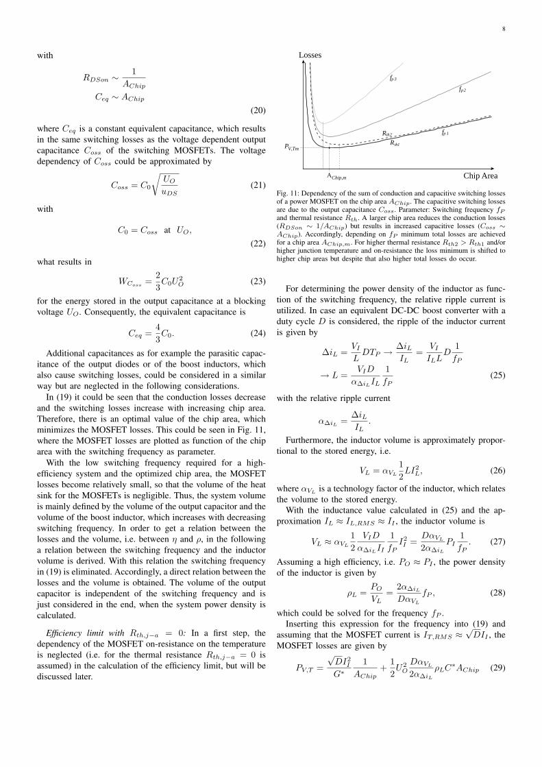
In (19) it could be seen that the conduction losses decreaseand the switching losses increase with increasing chip area.Therefore, there is an optimal value of the chip area, whichminimizes the MOSFET losses. This could be seen in Fig. 11,where the MOSFET losses are plotted as function of the chiparea with the switching frequency as parameter.
With the low switching frequency required for a high-efficiency system and the optimized chip area, the MOSFETlosses become relatively small, so that the volume of the heatsink for the MOSFETs is negligible. Thus, the system volumeis mainly defined by the volume of the output capacitor and thevolume of the boost inductor, which increases with decreasingswitching frequency. In order to get a relation between thelosses and the volume, i.e. between η and ρ, in the followinga relation between the switching frequency and the inductorvolume is derived. With this relation the switching frequencyin (19) is eliminated. Accordingly, a direct relation between thelosses and the volume is obtained. The volume of the outputcapacitor is independent of the switching frequency and isjust considered in the end, when the system power density iscalculated.
Efficiency limit with Rth,j−a = 0: In a first step, thedependency of the MOSFET on-resistance on the temperatureis neglected (i.e. for the thermal resistance Rth,j−a = 0 isassumed) in the calculation of the efficiency limit, but will bediscussed later.
Chip Area
Losses
fp 3
fp2
fp 1
Rth1
Rth2
PV,Tm
ΑChip,m
Fig. 11: Dependency of the sum of conduction and capacitive switching lossesof a power MOSFET on the chip area AChip. The capacitive switching lossesare due to the output capacitance Coss. Parameter: Switching frequency fPand thermal resistance Rth. A larger chip area reduces the conduction losses(RDSon ∼ 1/AChip) but results in increased capacitive losses (Coss ∼AChip). Accordingly, depending on fP minimum total losses are achievedfor a chip area AChip,m. For higher thermal resistance Rth2 > Rth1 and/orhigher junction temperature and on-resistance the loss minimum is shifted tohigher chip areas but despite that also higher total losses do occur.
For determining the power density of the inductor as func-tion of the switching frequency, the relative ripple current isutilized. In case an equivalent DC-DC boost converter with aduty cycle D is considered, the ripple of the inductor currentis given by
∆iL =VILDTP →
∆iLIL
=VIILL
D1fP
→ L =VID
α∆iLIL
1fP
(25)
with the relative ripple current
α∆iL =∆iLIL
.
Furthermore, the inductor volume is approximately propor-tional to the stored energy, i.e.
VL = αVL12LI2
L, (26)
where αVL is a technology factor of the inductor, which relatesthe volume to the stored energy.
With the inductance value calculated in (25) and the ap-proximation IL ≈ IL,RMS ≈ II , the inductor volume is
VL ≈ αVL12
VID
α∆iLII
1fPI2I =
DαVL2α∆iL
PI1fP
. (27)
Assuming a high efficiency, i.e. PO ≈ PI , the power densityof the inductor is given by
ρL =POVL
=2α∆iL
DαVLfP , (28)
which could be solved for the frequency fP .Inserting this expression for the frequency into (19) and
assuming that the MOSFET current is IT,RMS ≈√DII , the
MOSFET losses are given by
PV,T =√DI2
I
G∗1
AChip+
12U2O
DαVL2α∆iL
ρLC∗AChip (29)

9
with
RDSon =1G∗
1AChip
Ceq = C∗AChip.
There, G∗ is the conductivity per unit area and C∗ is theequivalent capacitance per unit area.
Equation (29) could be summarized to
PV,T = βR1G∗
P 2O
1AChip
+ βCρLC∗AChip (30)
with
βR =√D
U2O(1−D)2
βC =12U2O
DαVL2α∆iL
,
where it could be seen that the conduction losses are decreas-ing and the switching losses are increasing with increasingchip area AChip. Therefore, there is an optimal chip arearesulting in minimal overall losses and equal conduction andswitching losses. The optimal area is
AChip,opt =
√βR
βCρLG∗C∗PO. (31)
Inserting this expression into (30) and assuming again a highefficiency (PO ≈ PI ) results in
PV,T,m = γV
√ρLC∗
G∗PO ≈ γV
√ρLC∗
G∗PI (32)
with
γV = 2√βRβC . (33)
Since PV,T /PI = 1− η, the maximal achievable efficiency ata given power density is
(1− η) = γV
√ρL
FOMηρ1(34)
with
FOMηρ1 =
√G∗
C∗,
when considering the MOSFET losses and the inductor vol-ume. There,
√G∗/C∗ is the Figure of Merit FOMηρ1 (with
the unit√
Hz) reflecting the performance of the switch tech-nology. The higher the conductance and the lower the parasiticcapacitance of the switch is, the higher is the maximal achiev-able efficiency. Furthermore, the power density of the inductoris limiting the efficiency. With increasing switching frequencythe inductor volume decreases, i.e. the power density increases.However, the efficiency is decreasing due the higher switchinglosses.
Efficiency limit with Rth,j−a > 0: So far, the increase ofthe on-resistance of the MOSFET in (19) due to the increasingjunction temperature, which is rising with increasing losses,
0 20 40 60 80 100 120 140 160 180 2000
10
20
30
40
50
60
70
80
Junction Temperature [°C]
FOM
2 hr,1
= G
* /C
* [10
9 s-1
] IPB Si CoolMOS500 V SiC JFET
Fig. 12: Dependency of the power density Figure-of-Merit FOMηρ1
=√G∗/C∗ of a 650V Si CoolMOS IBP60R099CP (Infineon, chip area
28mm2) and of a 500V (620V avalanche voltage) SiC J-FET (SiCED,normally on, 5.75mm2) on the junction temperature. In both cases thecalculation of G∗ and C∗ is based on the total chip area, i.e. the arearequired for edge termination is not subtracted). Parameters for Tj=75Cand UO=400V: CoolMOS: 4.2 Ohm*mm2, 5.1 pF/mm2; SiC J-FET: 1.7Ohm*mm2, 11.6 pF/mm2.
has been neglected. The on-resistance as function of temper-ature is given by
RDSon = RDSon,25 (1 + α∆Tj)= RDSon,25 (1 + αPV,TRth,j−a) . (35)
This relation is inserted in (19) and the resulting expressionsolved for the losses PV,T resulting in
PV,T =RDSon,25I
2RMS + 1/2fPCeqU
2O
1−RDSon,25αRth,j−aI2RMS
. (36)
Again, the on-resistance RDSon,25 and the effective capaci-tance are dependent on the chip area AChip, so that an optimalchip area exists which results in minimal losses. Similar to(30),
PV,T =βRP
2O + βCρLC
∗G∗AChip2
G∗AChip − βRP 2OαRth,j−a
(37)
is resulting for the losses as function of AChip. Optimizingthe chip area for minimal MOSFET losses results in
AChip,opt =POγν
4βCρLG∗C∗
(ρLC
∗αRth,j−aPOγν
+√ρLC∗
√α2R2
th,j−aC∗P 2
Oγ2νρL+4G∗
). (38)
Analogously to (34), this results in
(1− η) =γν√ρL
FOMηρ1
(POγν
√ρL
12FOMηρ2
Rth,j−a
+
√1 + ρLP 2
Oγ2ν
14FOM2
ηρ2
R2th,j−a
)(39)
with
FOMηρ2 =
√G∗
C∗1α

10
There, the original figure of merit FOMηρ1 =√G∗/C∗ as
well as the new figure of merit FOMηρ2 reflecting the cool-ing conditions of the semiconductor determine the maximalachievable efficiency. The lower the dependency of RDSonon the temperature and/or the lower the thermal resistancebetween the junction and the ambient is, the smaller is theinfluence of the second figure of merit and the higher is themaximal efficiency. With increasing α or Rth,j−a the squareroot dependency of the minimal losses on ρL changes to amore linear dependency.
In the calculations it has been assumed, that the thermal re-sistance is independent of the chip area, what is true in case thethermal resistance is mainly determined by the case-to-ambientresistance as this is the case for PCB mounted MOSFETs. Incase of a forced air cooling the total thermal resistance ismainly determined by the junction-to-case resistance, whichis also dependent on the chip area. A similar calculation asexplained above could be performed in this case. However,this leads to relatively lengthy expressions, which are omittedhere for the sake of brevity.
B. Input Inductor
Besides the semiconductors, the magnetic components arethe main cause for losses in the PFC system. There, thelosses of the magnetic components decrease with increasingvolume, as will be shown in the following by a simplifiedconsiderations, where only a purely sinusoidal current IRMS
is assumed in the inductor and where HF effects are neglected.This basic tendency, however, is also valid in case the HFeffects are included as verified with numeric calculations andcould be used to describe the dependency of the losses in thePFC inductor on the inductor volume.
First, the core losses are expressed as function of thegeometry and the Steinmetz parameters, which can be obtainedfrom the data sheets of the core material.
PCo = CBβfαVCo
= C
(UT
NACo
)βfαAColCo
= C
(U
N
)βfα−β
1√kCW
kSCA32−βCo (40)
with
kCW =ACoAW
kSC = Shape Factor of Core.
Second, the winding losses neglecting the HF-effects arecalculated as function of geometry.
PWdg = RW I2RMS =
N2lWσAW kCU
I2RMS
=N2kCW kSW
σ√ACokCU
I2RMS (41)
with
kSW = Shape Factor of Winding.
Since the winding losses increase with the number of turnsN and the core losses decrease with N , there is an optimalnumber of turns NOpt resulting in minimal losses. This NOptis calculated in the third step and then used to eliminate N inthe winding and core loss equations.
By minimizing PCo+PW as function of N with respect tothe losses one obtains
NOpt = UI D 2−1
2+β (42)
·
(A2β−4Co k3
CWU4ID
4k2SW I
4I,RMSf
−2α+2β
C2 β2 k2SC σ
2
) −14+2β
for the optimal number of turns.For relating the losses and the inductor volume, the core
and the winding volume are expressed by
VCo = ACokSC√AW = A
32W kCW kSC (43)
VW = AW kSW√ACo = A
32W kSW
√kCW . (44)
Solving this for the core area and setting VL = VCo + VWresults in
ACo = kCW
(VL
kCW kSC + kSW√kCW
) 23
. (45)
Inserting the optimal number of turns and the expression forthe core losses in the sum of (40) and (41) and summarizingthe constants in k∑ = f(β) results in the total losses
PL = k∑V 4(2−β)3(2+β)−
13
L f2α−2β2+β I
2β2+βRMSU
2β2+β . (46)
Assuming for example β = 2 and α = 1 results in
PL ∼UIRMS√fV
13L
(47)
which shows that the losses decrease with an increasinginductor volume.
This tendency is also verified in case a more comprehensivemodel for the losses is used, what could be seen in Fig. 13,
Volume [dm3]
Loss
es [W
]
Skin-EffektProximity
CoreTotal
60
50
40
30
20
10
00.1 0.2 0.3 0.4 0.50
Fig. 13: Winding losses, i.e. resistive losses considering skin and proximityeffect and core losses of an inductor in dependency of the inductor volume.The core geometry is optimized for minimum total losses; winding lossesdue to the fringing field of the air gap are not considered. An increase of theoverall inductor volume results in a reduction of the total losses.

11
where the losses of an inductor utilizing an E-Core and litz-wire are shown in dependency of the inductor volume. Inthe loss calculations the skin- and the proximity-effect lossesbut not the losses due to the fringing field of an air gap areconsidered (1-D approach [26]). The current is assumed tobe 20A and the inductor voltage to be sinusoidal with anamplitude of 300V and a frequency of 100kHz.
As the losses in the inductor monotonically decrease withincreasing volume, the inductor volume must be limited duringthe minimization of the system losses (cf. Chapter V). Thisindirectly influences also the optimal operating frequency andthe power density of the system.
C. Output Capacitor
For the output capacitor either electrolytic or film capacitorscould be used. With electrolytic capacitors a higher powerdensity is achieved due to the higher capacitance per volume.However, the losses in the electrolytic capacitors due to theESR and the leakage current are significantly higher than withfilm capacitors. Thus, film capacitors are required for high effi-ciency designs as considered in this paper. The film capacitorsalso have a higher ripple current rating per capacitance.
In the following both technologies are shortly investigatedwith respect to achievable power density. There, a hold up timerequirement is not considered, so that the capacitance value isdetermined by the ripple voltage in case of the film capacitorand by the ripple current in case of the electrolytic capacitor. Incase a hold up time has to be provided, the capacitance valueis determined by this requirement, which directly results in avolume for the capacitors.
1) Film Capacitors: With film capacitors, the volume scaleslinearly with the stored energy [3] since the thickness ofthe capacitor is mainly determined by the thickness of thedielectric layers. Therefore, the volume could be calculatedby
VCF = γ−1VCF
12CFU
2O, (48)
where γ−1VCF
(energy per volume) is the proportionality factorbetween the energy and the volume. In case the outputvoltage UO is fixed the volume just scales with the requiredcapacitance value CF .
In the considered case, the output voltage is fixed andthe capacitance value is determined by the ripple voltage.Approximating the capacitor current by a sinusoidal currentwith an amplitude equal to the average output current, therelative peak-to-peak output voltage ripple is given by
α∆uCF =uCFUO
=PO
4ωN1
12CFU
2O
=PO
4ωN1
γVCF VCF. (49)
This could be directly converted to
ρCF =POVCF
= 4ωNα∆uCF γVCF = γCF γVCF (50)
with
γCF = 4ωNα∆uCF
for the power density of the output capacitors based on filmtechnology.
2) Electrolytic Capacitors: In contrast to the film capaci-tors, which have a constant energy density, the energy densityof electrolytic capacitors scales approximately linearly withthe output voltage [3]. Assuming a constant output voltage,the energy density is fixed as with the film capacitor and thevolume linearly depends on the capacitance value. As alreadymentioned, the capacitance value of the output capacitor ismainly determined by the ripple current in case of electrolyticcapacitors and no hold up time requirements. Thus, the volumeof the electrolytic output capacitor is proportional to the ripplecurrent
VCE = γ−1VCE
IC,RMS . (51)
The ripple current could be directly related to the output power
I2C,RMS=
1M
(4
3π− 1
4M
)I2N ≈
2MU2O
(4
3π− 1
4M
)P 2O, (52)
where M is the modulation index. With this relation the powerdensity of electrolytic capacitors is given by
ρCE =POVCE
=UO√
8M3π −
12
γVCE = γCEγVCE . (53)
D. Cooling SystemThe cooling system is a major limitation for the achievable
power density, especially in case the efficiency is low, so thata large amount of heat has to be dissipated. The losses in thesemiconductor can be expressed as function of the efficiency
PV = (1− η)PI = (1− η)POη
(54)
but can also be related to the temperature drop and the thermalresistance of the heat sink
PVRth = ∆T ⇒ PV =∆Ts−aRth
= ∆Ts−aGth (55)
With the cooling system performance index (CSPI) defined in[31], the Rth is directly related to the volume of the heat sinkby
CSPI =1
RthVH=GthVH
. (56)
With the CSPI the losses are given by
PV =1− ηη
PO = ∆Ts−a CSPI VH , (57)
what finally results in the power density determined by theheat sink
ρH =POVH
= ∆Ts−a CSPIη
1− η. (58)
There, it could be seen that the power density is dominatedby the heat sink in case of a low efficiency, which is basicallynot desirable, and that the power density reaches 0 for η = 0.With increasing efficiency the influence of the heat sink onthe system power density decreases and the power density ofthe heat sink theoretically goes to infinity if the losses of thefan are neglected.

12
Output Diode + MOSFETs considering Rth & Inductor
& Output Capacitor
Heat Sink
Power Density [kW/dm3]
Effic
ienc
y [%
]
f=500kHz
f=100kHzf=50kHz
f=20kHz
η−ρ−Limit Scaled with respect to
power density
Heat Sink & Output Capacitor
Heat Sink
Heat Sink & Output Capacitor
Power Density [kW/dm3]
Effic
ienc
y [%
]
f=500kHz
f=100kHz
f=50kHzf=20kHz
Output Diode + MOSFETs & Inductor
Output Diode + MOSFETs considering Rth & Inductor
& Output Capacitor
b)
a)
Output Diode + MOSFETs & Inductor
η−ρ−Limit Scaled with Respect to
Power Density
Fig. 14: Calculated performance limits of the dual-boost PFC rectifier(Fig. 9b)) in the η-ρ-plane for a high-efficiency design a) and a high powerdensity design b). The assumed parameters (i.e. number of power MOSFETsand freewheeling diodes operating in parallel, output capacitance, etc.) arein accordance with the experimental systems described in Sections VI-A andVI-B). The cooling system performance index is based on the heat sink ICKS 40×40×20 by Fischer – in case of the ultra-compact system with andin case of the ultra-efficiency system without fan. The performance limitsare defining a theoretical Feasible Performance Space which cannot be fullyutilized concerning power density due the missing spatial integration of thecomponents available for the system realization; the practical performancelimit shown by a dash-dot line.
E. System Control and Auxiliary Supply
In addition to the main components also the control aswell as the sensors and the gate drives cause losses, whichare relatively independent of the operating point and systemdesign. These constant losses result in a fixed efficiencyreduction
∆ηaux =PauxPI≈ Paux
PO, (59)
which is a horizontal line in the η-ρ-plane. Also the leakagecurrent in case of employing electrolytic capacitors for theoutput capacitor causes constant losses, which have to beadded to the auxiliary power.
F. Overall System
In the previous paragraphs the different limitations in the η-ρ-plane caused by the semiconductors, the cooling system, theoutput capacitor and the auxiliary power have been discussed.In Fig. 14 the limiting lines for the parameters of a highly
efficient (cf. section VI-A) and for the parameters of an ultra-compact system (cf. Section VI-B) are depicted.
For obtaining the limiting curve considering all influencesat the same time, the equations for the power densities andefficiencies of the previous paragraphs have to be combined.There, losses which are not directly related to a volume (e.g.semiconductor losses without heat sink) or volumes which arenot directly related to losses (e.g. output capacitor volume)can simply be combined to a single curve.
Adding for example the volume of the cooling system (cf.IV-D) and the volume of the output capacitors (cf. IV-C)results in∑
Vν = VH + VC
=1
∆Ts−a CSPI(1− η)
POη
+POρC
. (60)
There, ρC stands either for ρCE or for ρCF depending on theapplied technology for the output capacitors.
This results in the new power density
ρHC =POVHC
=ρHρCρH+ρC
=γCγVC1
1 + γCγVCδTs−aCSPI
1−ηη
, (61)
which gives the same results as just for the output capacitorsin case of high CSPI values. For η = 1 the heat sink vanishesand the power density of the capacitor results and for η = 0the heat sink dominates, so that the power density decreasesto 0.
In general, the system power density could be calculated by
ρges =1∑i
1ρi
, (62)
where ρi are the power densities of the different components.However, this expression does not directly relate the powerdensity with the efficiency. For plotting the limit of the systemit is better to calculate all volumes and losses as function offrequency, then add the volumes and the losses and finallymake a parametric plot, with fP as parameter. The result ofthis calculation is shown in Fig. 14 as the η-ρ-limit of thesystem for two sets of parameters – one for the ultra-efficientand one for the ultra-compact system.
Since in the calculation of the volumes only the net volumesof the individual components are considered and the volumerequired for mounting or the volume lost due to the not match-ing component shapes are not considered, the actually resultingsystem volume is smaller than the sum of the net componentvolumes. In order to account for this, the volumes have beenincreases by 1/3 based on experience with experimental systems[4].
V. NUMERICAL OPTIMIZATION
After fundamental clarification of the limits in the η-ρ-planein Section IV, a numerical maximization of the efficiencyof the PFC rectifier system will now be performed. In theoptimization more detailed models of the inductors and semi-conductor losses are utilized, so that an analytical solutionfor the optimal set of parameters is not possible. The degreesof freedom are the switching frequency fP , the geometry of

13
the boost inductance, and the power semiconductor chip areaAChip, i.e. the number of power MOSFETs and SiC diodesconnected in parallel for realization of a power transistor S1,S2 and/or a freewheeling diode D1, D2.
The optimization is carried out for nominal power, i.e.for the continuous conduction mode. To assure a constantrelative ripple of the input current, the inductance value ofthe boost inductor LDM is varied inversely proportional tothe switching frequency fP . The volume of the boost inductorLDM (Fig. 9b)) is limited to a fixed value (equal to the volumeof LDM in Section VI-A). Otherwise, the inductance volumewould grow in the course of the optimization above all limits,because of the decreasing losses with increasing volume (cf.Section IV-B).
In the following first the optimization procedure and theutilized models are explained and thereafter results of theefficiency optimization are presented.
A. Converter Model
In Fig. 15 a flowchart of the developed procedure foroptimizing the design variables (fP , chip area of MOSFETsand diodes, number of turns and geometry of boost inductor)is shown.
The starting point of the procedure are the specifications ofthe converter system as for example the input/output voltagesand the output power but also component limits as e.g.the maximal allowed flux density or the maximal junctiontemperature of the MOSFETs. Also the starting values of thedesign variables are set. With these values the currents/voltagesof all the components are calculated and the losses in thesemiconductor elements are determined. For the design of theboost inductor an inner optimization loop, which optimizesthe number of turns and the geometry of the core and thewinding for minimal losses, has been implemented. The globaloptimization algorithm adds the losses of the boost inductor,the CM-choke, and the semiconductors and varies then the freeparameters, so that the overall system losses become minimal.In the system losses also the losses in the control, in the outputcapacitor and the EMI filter, which are assumed to be constant,are included.
In the following shortly the equations for the currents andvoltages, the semiconductor losses as well as the magneticcomponents and the auxiliary power are summarized.
1) Semiconductors: The fundamental component of theinput current is given by
iN(1) = IN sin(ωN t) (63)
with
IN =PNUN
√2
where UN is the RMS value of the mains voltage and PN theinput power. In addition to the fundamental component theripple current
iN,r =12UOTPLDM
1M
sin(ωN t) sin(
1− 1M
sin(ωN t))
(64)
Spezification of the ParameterUN / UO / PO - BMax / CO /Rth,MOS /etc.
Electrical Model of the PFC Converter Currents / Voltages / Flux Density
Winding & Core Losses of the Inductor
as Function of Geomertry
Minimization of Inductor LossesSC: BBoost ≤ BMax // UBoost ≤ UMax
fp / φBoost fp / IS / IDIN
Global Optimization AlgorithmMinimization of the Losses
Inner Optimization
Loop
Modification of the Values
Initial Values: fp, NPara, LBoost, NBoost
Losses in the Semiconductors
ModifyComponents
Losses CM-Choke
Optimal Design
Fig. 15: Block diagram of the optimization procedure employed for maximiz-ing the efficiency of the dual-boost PFC rectifier (Fig. 9b). Considering Fig. 13an upper limit is defined for the boost inductor volume. All system specifica-tions and design constants, i.e. parameters of the specific on-resistance 1/G∗
and specific output capacitance C∗ of the power MOSFETs, the forwardcharacteristic of the freewheeling diodes, the thermal resistances of the powersemiconductors etc. are selected in accordance with the experimental systemin Section VI-A.
must be considered, where the modulation index M is definedas M = UO/
(√2UN
). With the input current fundamental
and the ripple current as well as the duty cycle
d = 1− 1M
sin(ωN t) (65)
the RMS current in the MOSFET and the average currentin the rectifier diodes are calculated. Based on the currentsthe conduction losses of the semiconductors are determined.There,
RDSon=RDSon,25+RDSon,125−RDSon,25
125C−25C(Tj−Ta) (66)
is used for calculating the conduction losses in dependency ofthe junction temperature (Ta is the ambient temperature). Bysolving
Tj − Ta =Rth,MOS
NP,MOS
(Pon + Poff +RDSonI
2RMS
)(67)
for the junction temperature Tj , the losses can directly becalculated, without any iteration. There, NP,MOS is thenumber of parallel connected MOSFETs and Pon/Poff arethe switching losses, which are calculated below. A similarequation is used for determining the junction temperature ofthe rectifier diodes, which influences the forward voltage drop.
The power transistors are controlled such, that each transis-tor is switching during half a mains period where the othertransistor is turn-on for minimizing the conduction losses.
In a next step, the current values at the turn-on and theturn-off of the MOSFET are determined based on the abovecalculated input current. The switched currents are requiredfor calculating the switching losses based on measured losscurves.

14
During the turn-on of the MOSFET the junction capacitanceof the freewheeling diode as well as parasitic capacitances ofthe wiring and the respective boost inductor are charged ordischarged. This results in a share of the turn-on losses, whichare independent of the current. This is also true for the outputcapacitance of a power transistor, which has to be dischargedduring the turn-on. Additionally, current dependent losses aregenerated in the switching transisitor, so that the overall turn-on losses are given by
Eon =12QSiCUONP,Dio + 4.32 · 10−6[Ws/A]IMOS(tk)
+12Ceq,MOSU
2ONP,MOS . (68)
The numeric values have been obtained by measurements onthe system shown in Fig. 20 and the components given inTable II.
Due to the large output capacitance of the parallel connectedMOSFETs ZVS conditions are given during turn-off, so thatthe turn-off losses are very small and neglected in the consid-erations. This is also true for the switching losses of the SiCSchottky diodes employed as freewheeling diodes. Thus, theswitching losses are mainly occuring during the turn-on of theMOSFETs.
2) Magnetic Components: Besides the semiconductors, theboost inductor is one of the major loss contributors. In theconsidered system the inductor is realized with foil windingsand the basic design of the inductors geometrically determinedby the four variables a, b, c and d as explained in [3]. Withthese variables for example the cross sectional area of the coreor the window could be expressed and the losses in the core orthe winding can be determined as function of these variables.This relation between the geometry and the losses enables thenan optimization of the number of turns and the geometry forminimal losses.
For calculating the winding losses first the harmonics of theboost inductor current are calculated with a Fourier analysis.The time behavior of the inductor current is determined with(63) and (64) and the switching times. With the amplitude andthe frequency of the harmonics the skin (69) and proximity(70) effect losses at each frequency are calculated with an 1-D approximation as for example presented in [26], [29], [30]and then – based on the orthogonality of the losses [32] – thelosses at the single harmonics IL(i) are added
PS =∑i
lW2σdh
I2L(i)
νi2
sinh νi + sin νicosh νi − cos νi
(69)
PP =∑i
∑m
dlW νiσh
sinh νi − sin νicosh νi + cos νi
H2S(i)m (70)
with
HS(i)m =2m− 1
4IL(i)
d.
For calculating the proximity effect losses in the inductor, itis assumed that there is a gap in all three legs, i.e. the H-fieldramps from −Hmax/2 to +Hmax/2. Furthermore, the lossesin the winding due to the fringing field of the gap are neglected
in order to simplify the calculations, what does not result ina too large error in the considered case as FEM simulationshave proven. In all the calculations the losses are expressed asfunction of the variables a, b, c and d, so that it is possible tooptimize the geometry of the core and the winding for minimallosses.
For the calculation of the core losses the flux densitytime behavior in the core must be determined. In the DMinductor the flux density follows a 50Hz major loop and minormagnetization loops with switching frequency. In such a casethe core losses can be calculated based on the method proposedin [27], where the Steinmetz coefficients [28] are utilized forcharacterizing the core material and where the rate of changeof the flux density (dB/dt) is the basis for the loss calculation.Here, these equations are applied and the losses are againdescribed as function of the geometry for the loss optimization.With UL,j and tj the voltage across the inductor is describedas a piece wise linear function.
PCore =ki(∆B)β−α
T
∑j
(UL,jNL ab
)α∆tjVC (71)
with
ki =k
2β+1πα−1(
0.2761 + 1.7061α+1.354
) (72)
In addition to the boost inductor, a CM-choke is used inthe converter for reducing the EM noise emission as shownin Fig. 9b). In the considered system, this CM-choke has thesame basic design as the boost inductor, so that the same basicequations for calculating the losses can be used as for the boostinductor. The time behavior of the current in the windings ofthe CM-choke is the same as for the boost inductors. However,the magnetic field required for calculating the proximity effectlosses is different, since this field is only generated by the CMcurrent. Due to the relatively small CM capacitors CCM,1 andCCM,2, the impedance of the capacitors at line frequency isrelatively high, so that the low frequency component of theCM voltage appears across the CM-capacitors. Consequently,the flux density in the core of the CM inductor is mainlydetermined by the switching frequency component of the CMvoltage 1/2uS,∼ (cf. Fig. 10). In the worst case ±UO/4 isapplied to the CM inductor with 50% duty cycle. In order tosimplify the calculation this situation is assumed to be presentover the whole fundamental period. This does not lead to asignificant error as the core losses of the CM inductor arerelatively low anyway.
During the optimization the flux density is kept below themaximal admissible level and the inductor volume is limitedto a defined value (cf. IV-B).
3) Output Capacitor & Auxiliary: For achieving a veryhigh efficiency also minor loss contributions must be consid-ered and minimized. There, for example the output capacitorscould have a significant loss share, if electrolytic capacitors areused, since the leakage current of these capacitors is relativelyhigh. Due to the ripple current several parallel connected
15
Switching Frequency [kHz]
Effic
ienc
y [%
]
Power D
ensity [kW/dm
3]
Calculated Ultra Efficient System Experimental Ultra
Efficient System
Scaled Power Density
Power Density
Efficiency
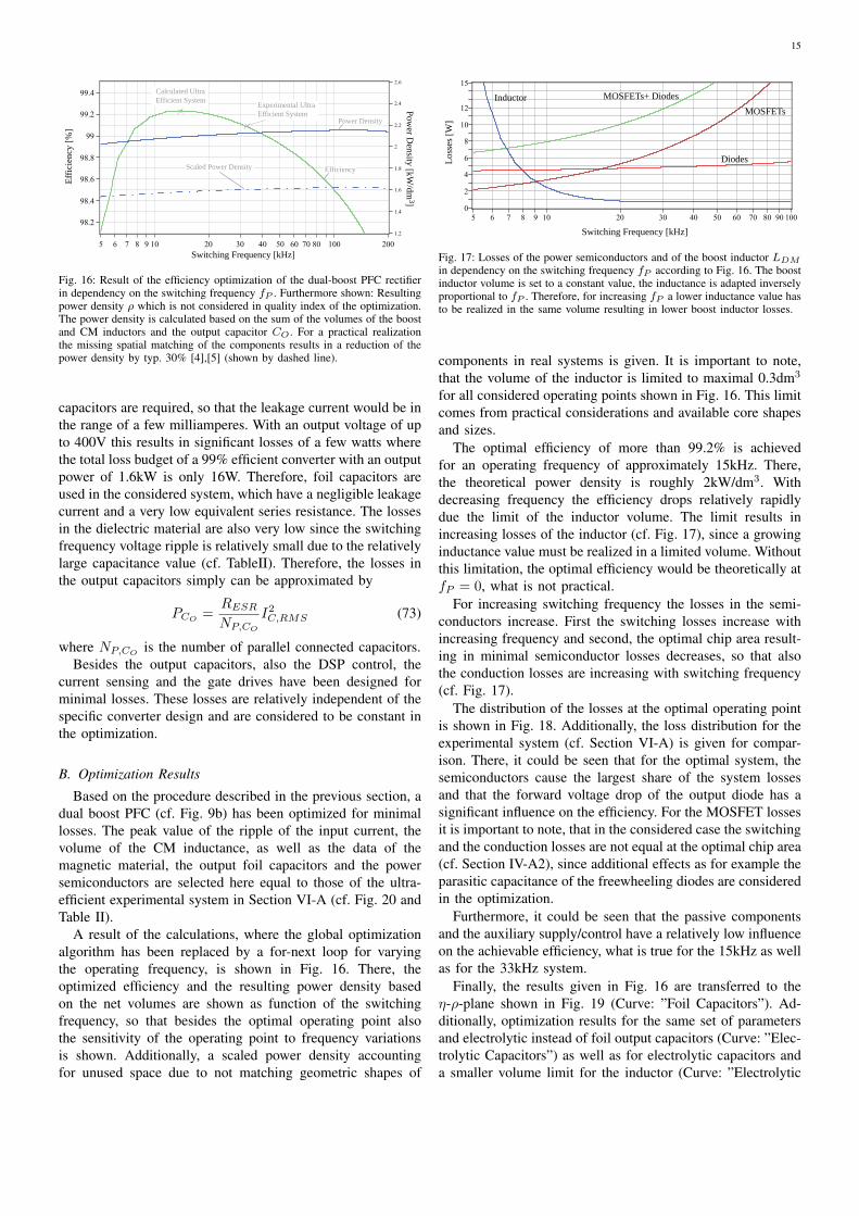
Fig. 16: Result of the efficiency optimization of the dual-boost PFC rectifierin dependency on the switching frequency fP . Furthermore shown: Resultingpower density ρ which is not considered in quality index of the optimization.The power density is calculated based on the sum of the volumes of the boostand CM inductors and the output capacitor CO . For a practical realizationthe missing spatial matching of the components results in a reduction of thepower density by typ. 30% [4],[5] (shown by dashed line).
capacitors are required, so that the leakage current would be inthe range of a few milliamperes. With an output voltage of upto 400V this results in significant losses of a few watts wherethe total loss budget of a 99% efficient converter with an outputpower of 1.6kW is only 16W. Therefore, foil capacitors areused in the considered system, which have a negligible leakagecurrent and a very low equivalent series resistance. The lossesin the dielectric material are also very low since the switchingfrequency voltage ripple is relatively small due to the relativelylarge capacitance value (cf. TableII). Therefore, the losses inthe output capacitors simply can be approximated by
PCO =RESRNP,CO
I2C,RMS (73)
where NP,CO is the number of parallel connected capacitors.Besides the output capacitors, also the DSP control, the
current sensing and the gate drives have been designed forminimal losses. These losses are relatively independent of thespecific converter design and are considered to be constant inthe optimization.
B. Optimization Results
Based on the procedure described in the previous section, adual boost PFC (cf. Fig. 9b) has been optimized for minimallosses. The peak value of the ripple of the input current, thevolume of the CM inductance, as well as the data of themagnetic material, the output foil capacitors and the powersemiconductors are selected here equal to those of the ultra-efficient experimental system in Section VI-A (cf. Fig. 20 andTable II).
A result of the calculations, where the global optimizationalgorithm has been replaced by a for-next loop for varyingthe operating frequency, is shown in Fig. 16. There, theoptimized efficiency and the resulting power density basedon the net volumes are shown as function of the switchingfrequency, so that besides the optimal operating point alsothe sensitivity of the operating point to frequency variationsis shown. Additionally, a scaled power density accountingfor unused space due to not matching geometric shapes of
Frequency [kHz]
Loss
es [W
]
Inductor MOSFETs+ Diodes
Diodes
MOSFETs
Switching Frequency [kHz]
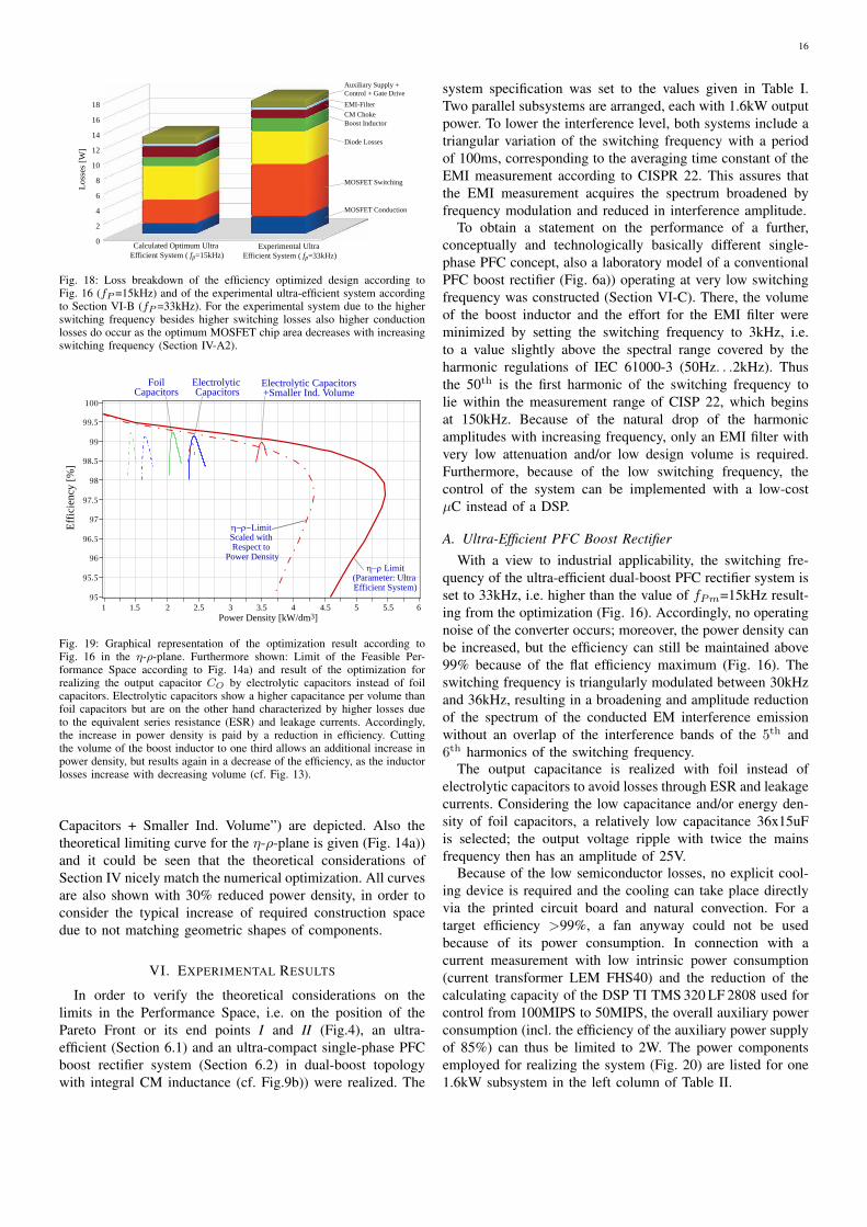
Fig. 17: Losses of the power semiconductors and of the boost inductor LDMin dependency on the switching frequency fP according to Fig. 16. The boostinductor volume is set to a constant value, the inductance is adapted inverselyproportional to fP . Therefore, for increasing fP a lower inductance value hasto be realized in the same volume resulting in lower boost inductor losses.
components in real systems is given. It is important to note,that the volume of the inductor is limited to maximal 0.3dm3
for all considered operating points shown in Fig. 16. This limitcomes from practical considerations and available core shapesand sizes.
The optimal efficiency of more than 99.2% is achievedfor an operating frequency of approximately 15kHz. There,the theoretical power density is roughly 2kW/dm3. Withdecreasing frequency the efficiency drops relatively rapidlydue the limit of the inductor volume. The limit results inincreasing losses of the inductor (cf. Fig. 17), since a growinginductance value must be realized in a limited volume. Withoutthis limitation, the optimal efficiency would be theoretically atfP = 0, what is not practical.
For increasing switching frequency the losses in the semi-conductors increase. First the switching losses increase withincreasing frequency and second, the optimal chip area result-ing in minimal semiconductor losses decreases, so that alsothe conduction losses are increasing with switching frequency(cf. Fig. 17).
The distribution of the losses at the optimal operating pointis shown in Fig. 18. Additionally, the loss distribution for theexperimental system (cf. Section VI-A) is given for compar-ison. There, it could be seen that for the optimal system, thesemiconductors cause the largest share of the system lossesand that the forward voltage drop of the output diode has asignificant influence on the efficiency. For the MOSFET lossesit is important to note, that in the considered case the switchingand the conduction losses are not equal at the optimal chip area(cf. Section IV-A2), since additional effects as for example theparasitic capacitance of the freewheeling diodes are consideredin the optimization.
Furthermore, it could be seen that the passive componentsand the auxiliary supply/control have a relatively low influenceon the achievable efficiency, what is true for the 15kHz as wellas for the 33kHz system.
Finally, the results given in Fig. 16 are transferred to theη-ρ-plane shown in Fig. 19 (Curve: ”Foil Capacitors”). Ad-ditionally, optimization results for the same set of parametersand electrolytic instead of foil output capacitors (Curve: ”Elec-trolytic Capacitors”) as well as for electrolytic capacitors anda smaller volume limit for the inductor (Curve: ”Electrolytic
16
Experimental Ultra Efficient System ( fp=33kHz)
Calculated Optimum Ultra Efficient System ( fp=15kHz)
18
16
14
12
10
8
6
0
Auxiliary Supply +Control + Gate DriveEMI-Filter
MOSFET Conduction
MOSFET Switching
Diode Losses
Boost InductorCM Choke
4
2
Loss
es [W
]
Fig. 18: Loss breakdown of the efficiency optimized design according toFig. 16 (fP =15kHz) and of the experimental ultra-efficient system accordingto Section VI-B (fP =33kHz). For the experimental system due to the higherswitching frequency besides higher switching losses also higher conductionlosses do occur as the optimum MOSFET chip area decreases with increasingswitching frequency (Section IV-A2).
Power Density [kW/dm3]
Effic
ienc
y [%
]
1.5 2.5 3.5 4.5 5.51 2 3 4 5 6
FoilCapacitors
Electrolytic Capacitors
Electrolytic Capacitors+Smaller Ind. Volume
η−ρ Limit(Parameter: Ultra Efficient System)
η−ρ−Limit Scaled with Respect to
Power Density
Fig. 19: Graphical representation of the optimization result according toFig. 16 in the η-ρ-plane. Furthermore shown: Limit of the Feasible Per-formance Space according to Fig. 14a) and result of the optimization forrealizing the output capacitor CO by electrolytic capacitors instead of foilcapacitors. Electrolytic capacitors show a higher capacitance per volume thanfoil capacitors but are on the other hand characterized by higher losses dueto the equivalent series resistance (ESR) and leakage currents. Accordingly,the increase in power density is paid by a reduction in efficiency. Cuttingthe volume of the boost inductor to one third allows an additional increase inpower density, but results again in a decrease of the efficiency, as the inductorlosses increase with decreasing volume (cf. Fig. 13).
Capacitors + Smaller Ind. Volume”) are depicted. Also thetheoretical limiting curve for the η-ρ-plane is given (Fig. 14a))and it could be seen that the theoretical considerations ofSection IV nicely match the numerical optimization. All curvesare also shown with 30% reduced power density, in order toconsider the typical increase of required construction spacedue to not matching geometric shapes of components.
VI. EXPERIMENTAL RESULTS
In order to verify the theoretical considerations on thelimits in the Performance Space, i.e. on the position of thePareto Front or its end points I and II (Fig.4), an ultra-efficient (Section 6.1) and an ultra-compact single-phase PFCboost rectifier system (Section 6.2) in dual-boost topologywith integral CM inductance (cf. Fig.9b)) were realized. The
system specification was set to the values given in Table I.Two parallel subsystems are arranged, each with 1.6kW outputpower. To lower the interference level, both systems include atriangular variation of the switching frequency with a periodof 100ms, corresponding to the averaging time constant of theEMI measurement according to CISPR 22. This assures thatthe EMI measurement acquires the spectrum broadened byfrequency modulation and reduced in interference amplitude.
To obtain a statement on the performance of a further,conceptually and technologically basically different single-phase PFC concept, also a laboratory model of a conventionalPFC boost rectifier (Fig. 6a)) operating at very low switchingfrequency was constructed (Section VI-C). There, the volumeof the boost inductor and the effort for the EMI filter wereminimized by setting the switching frequency to 3kHz, i.e.to a value slightly above the spectral range covered by theharmonic regulations of IEC 61000-3 (50Hz. . .2kHz). Thusthe 50th is the first harmonic of the switching frequency tolie within the measurement range of CISP 22, which beginsat 150kHz. Because of the natural drop of the harmonicamplitudes with increasing frequency, only an EMI filter withvery low attenuation and/or low design volume is required.Furthermore, because of the low switching frequency, thecontrol of the system can be implemented with a low-costµC instead of a DSP.
A. Ultra-Efficient PFC Boost RectifierWith a view to industrial applicability, the switching fre-
quency of the ultra-efficient dual-boost PFC rectifier system isset to 33kHz, i.e. higher than the value of fPm=15kHz result-ing from the optimization (Fig. 16). Accordingly, no operatingnoise of the converter occurs; moreover, the power density canbe increased, but the efficiency can still be maintained above99% because of the flat efficiency maximum (Fig. 16). Theswitching frequency is triangularly modulated between 30kHzand 36kHz, resulting in a broadening and amplitude reductionof the spectrum of the conducted EM interference emissionwithout an overlap of the interference bands of the 5th and6th harmonics of the switching frequency.
The output capacitance is realized with foil instead ofelectrolytic capacitors to avoid losses through ESR and leakagecurrents. Considering the low capacitance and/or energy den-sity of foil capacitors, a relatively low capacitance 36x15uFis selected; the output voltage ripple with twice the mainsfrequency then has an amplitude of 25V.
Because of the low semiconductor losses, no explicit cool-ing device is required and the cooling can take place directlyvia the printed circuit board and natural convection. For atarget efficiency >99%, a fan anyway could not be usedbecause of its power consumption. In connection with acurrent measurement with low intrinsic power consumption(current transformer LEM FHS40) and the reduction of thecalculating capacity of the DSP TI TMS 320 LF 2808 used forcontrol from 100MIPS to 50MIPS, the overall auxiliary powerconsumption (incl. the efficiency of the auxiliary power supplyof 85%) can thus be limited to 2W. The power componentsemployed for realizing the system (Fig. 20) are listed for one1.6kW subsystem in the left column of Table II.

17
Fig. 20: Laboratory prototype of the ultra-efficient 3.2kW dual-boost PFCrectifier according to Fig. 9b) composed of two interleaved 1.6kW units;overall dimensions: 275x130x85mm; output power density: 1.1 kW/l.
Fig. 21: Measured peak conducted EMI of the system depicted in Fig. 20. Inaddition to the integrated CM filtering LCM and CCM shown in Fig. 9b)a further CM filter stage and DM filter capacitor has been employed on themains side (Position I in Fig. 10) in order to ensure compliance with CISPR22-QP Class B.
By means of a calorimeter the efficiency of the system inthe nominal operating point was determined to be 99.1%. Theresolution of the efficiency measurement here is 0.01%. Thecalorimeter was calibrated with a comparative measurement.For this purpose, the system was placed with short-circuitedoutput in the calorimeter and fed with a low AC voltage.Here only losses occur which can be very precisely measuredelectrically (precision of 0.2%, at 0.1% voltage and currentmeasurement precision). The thermal conditions and air flowswithin the calorimeter are approximately the same as for thegeneration of output power. In contrast thereto, with a calcula-tion of the efficiency based upon an electrical measurement ofthe input and output power, the error would amount to max.±0.4%.
Overall, the 3.2kW system has dimensions of275×130×85mm and thus a power density of 1.1 kW/dm3.As shown in the optimization (Fig. 16), by lowering theswitching frequency to 20kHz and adjusting the number ofpower MOSFETs and SiC diodes connected in parallel, anincrease of the efficiency to 99.15% would be possible. By theuse of SiC freewheeling diodes of a new type (IDD08SG60C)with lower reverse recovery and/or junction capacitancecharge, a further improvement to 99.2% could easily beobtained.
B. Ultra-Compact PFC Boost Rectifier
In [3], a switching frequency of fP=810kHz was calculatedas giving the maximum power density for a 10kW three-phase PWM rectifier system (see Fig.30 in [3]). This frequencyvalue can also serve as a guideline for the realization ofa single-phase PWM rectifier system of maximum powerdensity having the same output power as the power of onephase of the three-phase system. However, as the practicalrealization of the high switching frequency system shows, forvery high switching frequency a high distortion of the rectifierinput voltage would occur in the region of the current zerocrossing [34]; this is due to the high output capacitance ofthe super-junction MOSFETs. Hence a switching frequencyof 450kHz is selected. Due to the very flat maximum of thepower density over fP , this means only a slight increase indesign volume. Moreover, the pulse-width modulation can thenbe accomplished directly by the DSP (TI TMS 320 LF 2808,100MIPS), without a FPGA. For lowering the level of theconducted EM interference emission, again a modulation ofthe switching frequency (±50kHz) is provided. In the rightcolumn of Table II, the main components of the system(Fig. 22) are listed for a 1.6kW unit.
The single power MOSFET used has for fP=450kHz an ap-proximately optimal chip area with regard to the best possiblecompromise between conduction and switching losses. For theCM filter inductor LCM , the same magnetic core is used asfor boost inductor LDM . The output capacitance is determinedby the permissible current loading capacity of the electrolyticcapacitors. Overall, the 3.2kW system exhibits at the nominalpoint an efficiency of 95.8%; the dimensions of the systemare 175×80×42mm, hence a power density of 5.5kW/dm3 isachieved. By optimization of the cooling system and magneticintegration of LDM and LCM , this value could be increasedto ≈7kW/dm3.
TABLE II: Components of the ultra-efficient and the ultra-compact dual-boostPFC rectifier. The heat sink of the ultra-compact system is ICKS 40×40×30Fischer, incl. fan, Rth =1.5K/W.
Ultra-Efficient Ultra-Compact
MOSFETs per Leg 5× IPP60R099 per Leg 1× IPW60R045(CoolMOS) 600V / 0.099Ω 600V / 0.045Ω
Diodes per Leg 5× IDB10S60C per Leg 1× CSD10060(SiC Schottky) 600V / 10 A 600V / 10A
CM-Choke 3mH / 2 × 9 turns 2 × 10 turnsLCM 3 × EELP 64 Core 1 × EILP 38 Core
Boost Inductor 1mH / 2 × 9 turns 2 × 10 turnsLDM 3 × EELP 64 Core 1 × EILP 38 Core
CCM1=CCM2 280nF (ceramic) 110nF (ceramic)Output Cap. 18×450V/15µF (AVX) 12×FFB 450V/82µF
Capacitor FFB from AVX KXG Nippon ChemiSecond Stage of the EMI Filter (inserted at I in Fig. 10a))
CDMI 2µF -LCMI 1.2mH 637µH (Vitroperm W409)CCMI 22nF 22nF (ceramic)CDMII 2µF 4×220nFLDMII - 2×10µH EF25 N87CDMIII - 1.76µF
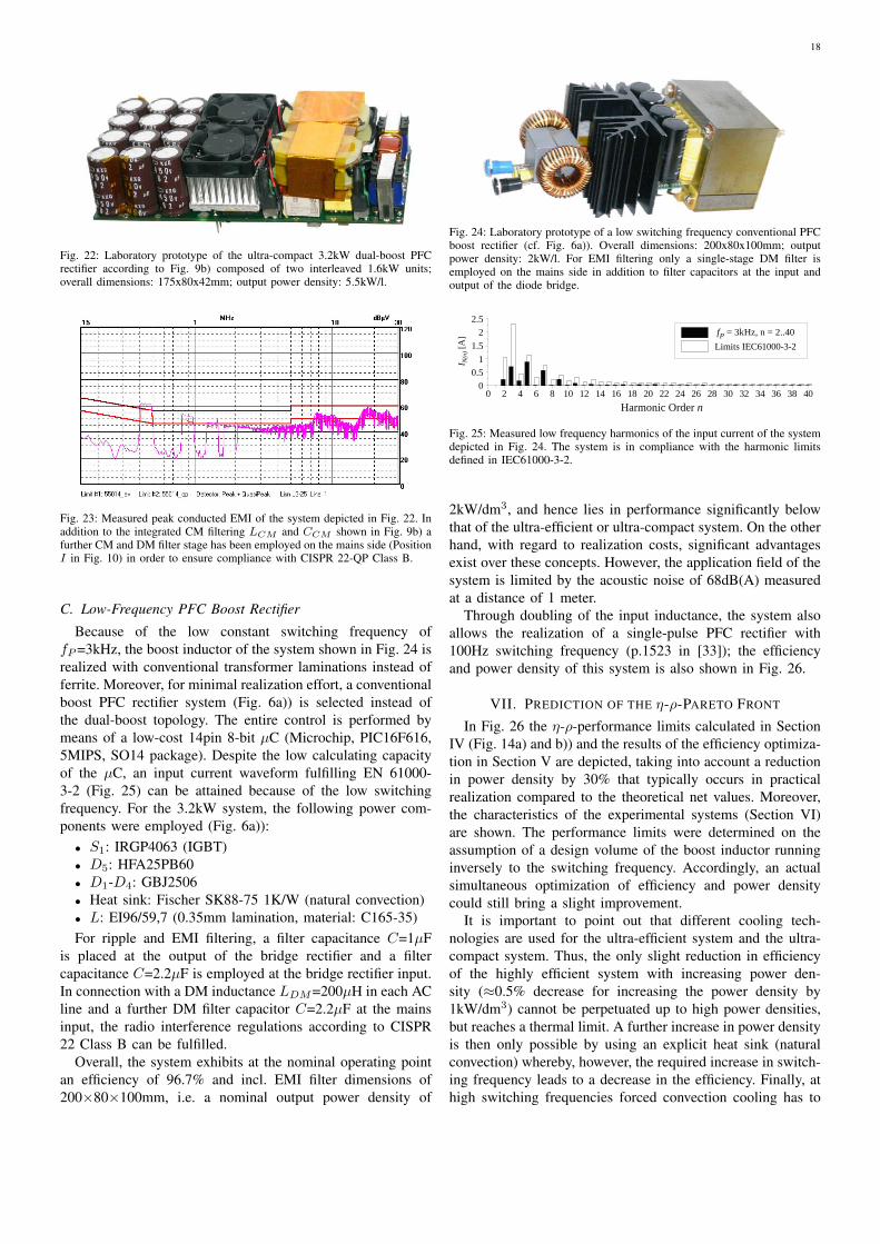
18
Fig. 22: Laboratory prototype of the ultra-compact 3.2kW dual-boost PFCrectifier according to Fig. 9b) composed of two interleaved 1.6kW units;overall dimensions: 175x80x42mm; output power density: 5.5kW/l.
Fig. 23: Measured peak conducted EMI of the system depicted in Fig. 22. Inaddition to the integrated CM filtering LCM and CCM shown in Fig. 9b) afurther CM and DM filter stage has been employed on the mains side (PositionI in Fig. 10) in order to ensure compliance with CISPR 22-QP Class B.
C. Low-Frequency PFC Boost Rectifier
Because of the low constant switching frequency offP=3kHz, the boost inductor of the system shown in Fig. 24 isrealized with conventional transformer laminations instead offerrite. Moreover, for minimal realization effort, a conventionalboost PFC rectifier system (Fig. 6a)) is selected instead ofthe dual-boost topology. The entire control is performed bymeans of a low-cost 14pin 8-bit µC (Microchip, PIC16F616,5MIPS, SO14 package). Despite the low calculating capacityof the µC, an input current waveform fulfilling EN 61000-3-2 (Fig. 25) can be attained because of the low switchingfrequency. For the 3.2kW system, the following power com-ponents were employed (Fig. 6a)):• S1: IRGP4063 (IGBT)• D5: HFA25PB60• D1-D4: GBJ2506• Heat sink: Fischer SK88-75 1K/W (natural convection)• L: EI96/59,7 (0.35mm lamination, material: C165-35)For ripple and EMI filtering, a filter capacitance C=1µF
is placed at the output of the bridge rectifier and a filtercapacitance C=2.2µF is employed at the bridge rectifier input.In connection with a DM inductance LDM=200µH in each ACline and a further DM filter capacitor C=2.2µF at the mainsinput, the radio interference regulations according to CISPR22 Class B can be fulfilled.
Overall, the system exhibits at the nominal operating pointan efficiency of 96.7% and incl. EMI filter dimensions of200×80×100mm, i.e. a nominal output power density of
Fig. 24: Laboratory prototype of a low switching frequency conventional PFCboost rectifier (cf. Fig. 6a)). Overall dimensions: 200x80x100mm; outputpower density: 2kW/l. For EMI filtering only a single-stage DM filter isemployed on the mains side in addition to filter capacitors at the input andoutput of the diode bridge.
0 2 4 6 8 10 12 14 16 18 20 22 24 26 28 30 32 34 36 38 400
0.51
1.52
2.5fP = 3kHz, n = 2..40Limits IEC61000-3-2
I N(n
) [A
]
Harmonic Order n
Fig. 25: Measured low frequency harmonics of the input current of the systemdepicted in Fig. 24. The system is in compliance with the harmonic limitsdefined in IEC61000-3-2.
2kW/dm3, and hence lies in performance significantly belowthat of the ultra-efficient or ultra-compact system. On the otherhand, with regard to realization costs, significant advantagesexist over these concepts. However, the application field of thesystem is limited by the acoustic noise of 68dB(A) measuredat a distance of 1 meter.
Through doubling of the input inductance, the system alsoallows the realization of a single-pulse PFC rectifier with100Hz switching frequency (p.1523 in [33]); the efficiencyand power density of this system is also shown in Fig. 26.
VII. PREDICTION OF THE η-ρ-PARETO FRONT
In Fig. 26 the η-ρ-performance limits calculated in SectionIV (Fig. 14a) and b)) and the results of the efficiency optimiza-tion in Section V are depicted, taking into account a reductionin power density by 30% that typically occurs in practicalrealization compared to the theoretical net values. Moreover,the characteristics of the experimental systems (Section VI)are shown. The performance limits were determined on theassumption of a design volume of the boost inductor runninginversely to the switching frequency. Accordingly, an actualsimultaneous optimization of efficiency and power densitycould still bring a slight improvement.
It is important to point out that different cooling tech-nologies are used for the ultra-efficient system and the ultra-compact system. Thus, the only slight reduction in efficiencyof the highly efficient system with increasing power den-sity (≈0.5% decrease for increasing the power density by1kW/dm3) cannot be perpetuated up to high power densities,but reaches a thermal limit. A further increase in power densityis then only possible by using an explicit heat sink (naturalconvection) whereby, however, the required increase in switch-ing frequency leads to a decrease in the efficiency. Finally, athigh switching frequencies forced convection cooling has to

19
Power Density [kW/dm3]
Effic
ienc
y [%
]Electrolytic Capacitors
Electrolytic Capacitors+Limited Ind. Volume
30kHz Exp. System
FoilCapacitors
Ultra CompactExp. System
Exp. Ultra Efficient System
( fp=33kHz)
3kHz Exp. System
100Hz Exp. System
η−ρ−Limit for Ultra
Compact System
η−ρ−Limit for Ultra
Efficient System
100
Fig. 26: Graphical representation of the performance of the experimentalsystems (Section V-B) in the η-ρ-plane in combination with the results of theefficiency optimization (Section V) and the η-ρ-performance limits calculatedin of Section IV (a reduction in power density by 1/3 due to the missingspatial matching of the components is considered, cf. Fig. 14). The theoreticalconsiderations are well predicting the actually achievable performance. Forhighly compact systems increasing the efficiency by 1% results in a decrease inpower density by ≈1kW/dm3. For ultra-efficient systems the same reductionof power density has to be accepted for improving the efficiency by 0.5%.
be used, whereby the power consumption of the fan causes adirect reduction in efficiency. However it is then possible toincrease the power density up to a higher thermal limit, againwith decreasing efficiency (typically 1% for each increase inpower density of 1kW/dm3).
VIII. SENSITIVITY ANALYSIS
In Fig. 27 the loss breakdown of the ultra-efficient and theultra-compact experimental systems is shown. By increasingthe switching frequency from 33kHz to 450kHz, primarily theswitching losses of the power MOSFETs and the power con-sumption of the gate-drive circuits are increased significantly.Furthermore, in order to keep the switching losses causedby the output capacitance of the power transistors low, thesemiconductor area used for each of the switches S1 and S2
must be reduced, which results in an increase of the conductionlosses. With a small design volume, the semiconductor lossescan then be dissipated only by forced convection cooling;because of the power consumption of the fans, thereby theefficiency is further reduced. Finally, the pulse pattern cal-culation at switching frequency requires the full calculation
Experimental Ultra Compact System
Experimental Ultra Efficient System
70
60
50
40
30
20
10
0
Output CapacitorAuxiliary Supply +Control + Gate Drive
EMI-Filter
MOSFETs Conduction
MOSFETs Switching
Boost Diodes
Boost InductorCM Choke
Loss
es [W
]
Fig. 27: Comparison of the breakdown of the power losses of the ultra-efficientand ultra-compact experimental dual-boost PFC rectifier.
capacity of the DSP used for control, which causes a higherpower consumption and hence an increase in the auxiliarypower. This shows that for high switching frequency or highpower density, a gain in efficiency would primarily be possibleby improvement of the FOMηρ1 =
√G∗/C∗ of the power
transistors and by means of a resonant gate drive. Alternatively,soft-switching concepts could be used whereby, however, asignificantly higher complexity would have to be accepted.
Apart from its use for determination of the best possibledesign, the optimization described in Section V can also beemployed for analyzing the sensitivity of the system perfor-mance with regard to selected design constants or technolog-ical parameters (Fig. 28). As the ultra-compact system, alsothe ultra-efficient system shows here a distinct dependenceof the losses on the parameters G∗ and C∗ of the powertransistors. Only a significant increase of the saturation limitof the magnetic core of the boost inductor could bring a com-parable reduction in losses or a comparable gain in efficiency,since then a lower switching frequency for a given designvolume of the inductor and thus lower losses of the powertransistors would be possible. If the switching frequency isset to a constant value above the audible limit, i.e. fP=20kHz(Fig. 28b)), this degree of freedom is eliminated and onlyG∗ and C∗ remain as main parameters for loss reduction.These considerations show clearly the possibility of studying
8
6
4
2
0
-2
-4
-6
-8
-10
4
2
0
-2
-4
-6
-8
-10
1/2
CEq
MO
SFET
1.5 x LBoost Inductor
1/2
CEq
MO
SFET
UO
= 38
0V
40
0V
1.5 x LBoost Inductor
1/2
R DS,
on M
OSF
ET
1/2
R th
MO
SFET
1/2
P Cor
e
B Sat
x 2
b)
a)
UO
= 38
0V
40
0V
1/2
R DS,
on M
OSF
ET
1/2
R th M
OSF
ET
1/2
P Cor
e
B Sat
x 2
Rel
ativ
e C
hang
e of
Los
ses [
%]
Rel
ativ
e C
hang
e of
Los
ses [
%]
Fig. 28: Relative change of the total losses of the ultra-efficient dual-boostPFC rectifier for changing the characteristic values of the power MOSFETs(equivalent output capacitance and on-resistance) and the parameters of themagnetic material employed for realizing the boost inductor (core losses andsaturation flux density). Furthermore, the influence of changing the outputvoltage level UO and the value of the boost inductor (×1.5) are considered.For a) the switching frequency is defined by the optimization procedure, forb) a constant switching frequency of fP =20kHz is assumed.

20
the effects of an improvement in technological characteristicson the system performance, which can be employed as a basisfor a targeted technology roadmapping.
IX. CONCLUSIONS
A reduction of the volume of an optimally designed inductorfor a given current load is always coupled with an increase inpower loss. Moreover, an increase of the switching frequencyleads to an increase of high-frequency losses and of the switch-ing losses of the power semiconductors, and hence finallyto a decrease in efficiency. The realization of ultra-efficientsystems is thus only possible at low switching frequenciesand only with acceptance of a relatively low power density.As shown in this paper by the example of an approximation ofthe η-ρ-Pareto Front of single-phase dual-boost PFC rectifiers,based on today's technology a maximum efficiency of typically99.2% can be attained at a power density of 1.1kW/dm3. In-creasing the switching frequency increases the power density;however, for an increase in the power density of 1kW/dm3, adecrease in efficiency by 0.5% has to be accepted. For forcedconvection cooled highly compact systems, the η-ρ-ParetoFront exhibits a larger gradient because of the increase of thelosses with the switching frequency. Here an increase of thepower density by 1kW/dm3 is connected with a decrease ofthe efficiency of typically 1%. With the use of all optimizationoptions, a maximum power density of ca. 7kW/dm3 at anefficiency of 97% could then be obtained.
The losses remaining in the efficiency maximum of ultra-efficient systems, with high design volumes and hence lowinductive losses, are mainly caused by the on-state voltagedrop of the freewheeling diodes and by the on-state lossesand capacitive switching losses of the power MOSFETs.If the frequency is to be kept above the audible limit, anefficiency increase is possible only through improvement ofthe FOMηρ1 =
√G∗/C∗ of the power transistors. It is of
interest here that SiC power transistors, assuming the presentstate of development, show no advantages over Si super-junction transistors (Fig. 12). The further development ofpower semiconductors thus is of major importance for furtherincreasing the efficiency.
If the power density is of secondary importance, the lossesin the boost inductor can be kept low by adequate design size.The properties of the magnetic materials are thus primarilyof importance when high efficiency and high power densityare demanded. A high saturation flux density enables herelow mean turn lengths and hence lower winding losses. Forlow hysteresis losses, a higher current ripple and a lowerinductance value are possible for same core losses, resultingin a lower design volume.
The present work is only an initial step into the areaof multi-objective optimization of single-phase PFC rectifiersystems. For further research a multitude of topics remains.For example, one would have to consider• a magnetic integration of the boost inductance LDM and
the common-mode inductance LCM (Fig. 9b)), or• a multi-stage realization of the integral CM filtering
for increasing the power density of the ultra-efficient system.Furthermore, the relatively coarse converter model, which is
20202009
Multi-Domain Modelling/OptimizationSystems-Oriented Analysis
Cross-Discipline Research/Hybrid SystemsWBG Power Semiconductors
Advanced Materials / PackagingModularization / Homogenous Power
Digital PowerMulti-Functional Integration / SMART Power
Microsystems Technologies
Super-Junction TechnologySimulation
Power MOSFETs/IGBTsMicroelectronics
Circuit TopologiesModulation Concepts
Control ConceptsSCRs / Diodes
Solid-State Devices
Fig. 29: Progress steps of solid state power electronics and related enablingtechnologies. Multi-domain modeling and optimization is a key element forensuring a further highly dynamic development of the area.
the basis of the optimization performed in this paper, could beexpanded by a model of the EMI filter, which at high powerdensity takes up typically 30% of the total volume of the con-verter. On this basis, a full multi-objective optimization withregard to efficiency and power density could be performed,i.e. the η-ρ-Pareto Front could be calculated directly. Furtherpossibilities would be:• to extend the optimization, which up to now has been
referred to the nominal power, to the efficiency at 20%,50% and 100% nominal power, in order to obtain a highefficiency over the entire output power range. Further-more,
• a parallel connection of subsystems could be consideredand their number optimized, whereby the operation ofan individual system would have to be possible either inthe continuous conduction mode or in the discontinuousconduction mode.
• Finally, the optimized distribution of a required totaloutput power over the subsystems could be consideredin such a way that minimal overall losses are assured foreach output power level.
In future, multi-objective optimization will assume greatimportance in power electronics research. Only by means of amathematical model often non-linear effects of parameters likethe switching frequency or the magnetic flux density swingcan be understood and the best possible compromise foundbetween competing optimization demands. Here, apart fromefficiency and volume, the weight must be seen as an importantperformance index, especially for mobile applications. Theincrease in the weight of a power electronics converter causesin some cases only a slight increase in the overall weight, butcan significantly raise the efficiency of the energy conversionand thus considerably increase the mission capability. Further-more, the thermal cycling capability should be considered as aperformance index, since the converter often represents a corecomponent and is of central importance for the functioning oflarger systems.
Finally, the Pareto Fronts and/or Pareto Surfaces should bedetermined in the Performance Space for different converterconcepts, which on the one hand gives a representation of

21
the chosen circuit topology and of the modulation conceptetc., and on the other hand of the component technologiesemployed. A performance comparison of competing conceptsis thus directly possible. Furthermore, before the conception ofa technology roadmap, different changes in a technology couldbe simply tested for their effect on the target performance, i.e.regarding their effectiveness. For this reason, multi-domainmodeling and optimization has to be seen as an essentialelement of a continued highly dynamic development of powerelectronics (Fig. 29).
ACKNOWLEDGMENT
The Authors would like to acknowledge the contributionof Thomas Friedli, Ph.D. student at the Power ElectronicSystems Laboratory of the ETH Zurich, who calculated thecharacteristic values G∗ and C∗ of Si CoolMOS and SiCJ-FETs based on datasheet values, measurement results andphysical models in order to determine the characteristic of theFOMηρ1 of both devices in dependency of the junction tem-perature. Furthermore, the support of Dr. G. Deboy, InfineonTechnologies AG, with providing power transistor samples forthe experimental systems is highly appreciated.
REFERENCES
[1] U.S. Department of Energy, Office of Integrated Analysisand Forecasting, International Energy Outlook 2008;www.eia.doe.gov/oiaf/ieo/index.html
[2] Ohashi, H., “Research Activities of the Power Electronics ResearchCenter with Special Focus on Wide Band Gap Materials,” Proceedingsof the 4th Conference on Integrated Power Systems, Naples, Italy, pp.153 - 156, 2006.
[3] Kolar, J.W., Drofenik, U., Biela, J., Heldwein, M.L., Ertl, H., Friedli,T., and Round, S.D., “PWM Converter Power Density Barriers,” Pro-ceedings of the 4th Power Conversion Conference (PCC'07), Nagoya,Japan, April 2 - 5; furthermore published in condensed form in IEEJTransactions on Industry Applications, No. 4, pp. 468 - 480.
[4] Biela, J., Badstuebner, U., and Kolar, J.W., “Design of a 5kW 1U10kW/ltr. Resonant DC-DC Converter for Telecom Applications,” Pro-ceedings of the 29th IEEE International Telecommunications EnergyConference, Sept. 30 - Oct. 4, pp. 824 - 831, 2007.
[5] Badstuebner, U., Biela, J., Faessler, B., Hoesli, D., and Kolar, J.W.,“An Optimized 5kW 147 W/in3 Telecom Phase-Shift DC-DC Converterwith Magnetically Integrated Current Doubler,” Proceedings of the 24th
IEEE Applied Power Electronics Conference, Washington DC, USA,February 15-19, pp. 21-27, 2009.
[6] Biela, J., Badstuebner, U., and Kolar, J.W., “Impact of Power DensityMaximization on Efficiency of DC-DC Converter Systems,” IEEE Trans-actions on Power Electronics, Volume 24, Issue 1, January, pp. 288-300,2009.
[7] Wu, C.J., Lee, F.C., Balachandran, S., and Goin, H.L., “Design Opti-mization for a Half Bridge DC-DC Converter,” IEEE Transactions onAerospace and Electronic Systems, Vol. AES-18, No. 4, pp. 497 - 508(1982).
[8] Busquets-Monge, S., Soremkun, G., Hertz, E., Crebier, C., Ragon, S.,Borojevich, D., Gurdal, Z., Arpilliere, M., and Lindner, D.K., “PowerConverter Design Optimization - A GA-Based Design Approach toOptimization of Power Electronics Circuits,” IEEE Industry ApplicationsMagazine, No. 1, pp. 32 - 39, 2004.
[9] Kumar, P., “A Framework for Multi-Objective Optimization and Multi-Objective Decision Making for Electrical Drives,” Ph.D. Thesis, Tech-nical University Delft, The Netherlands, 2008.
[10] Ali, S., Wilcock, R., Wilson, P., and Brown, A., “Yield Model Charac-terization for Analog Integrated Circuit using Pareto-Optimal Surface,”Proceedings of the 15th IEEE International Conference on Electronics,Circuits and Systems, pp. 1163 - 1166, 2008.
[11] Huber, L., Jang, Y., and Jovanovic, M., “Performance Evaluation ofBridgeless PFC Boost Rectifier,” IEEE Transactions on Power Electron-ics, Vol. 23, No. 3, pp. 1381 - 1390, 2008.
[12] Feng, B., and Xu, D., “1kW PFC Converter with Compound ActiveClamping,” IEEE Transactions on Power Electronics, Vol. 20, pp. 324 -331, 2005.
[13] Jovanovic, M., and Jang, Y., “State-of-the-Art Single-Phase ActivePower Factor Correction Techniques for High Power Applications - AnOverview,” IEEE Transactions on Industrial Electronics, Vol. 52, No. 3,pp. 701 - 708, 2005.
[14] Depenbrock, M., “Einphasen-Stromrichter mit sinusformigem Netzstromund gut geglatteten Gleichgrossen (in German),” ETZ-A, Bd. 94, H. 8,pp. 466-471, 1973.
[15] Ye, H., Yang, Z., Dai, J., Yan, C., Xin, X., Ying, J., “Common ModeNoise Modeling and Analysis of Dual Boost PFC Circuit,” Proceedingsof the 26th IEEE Intern. Telecommunications Energy Conference, Sept.19 - 23, pp. 575 - 582, 2004.
[16] Souza, A.F., and Barbi, I., “High Power Factor Rectifier with ReducedConduction and Commutation Losses,” Proceedings of the 21st IEEE In-ternational Telecommunications Energy Conference, Copenhagen, Den-mark, June 6 - 9, Paper 8-1, 1999.
[17] Jang, Y., and Jovanovic, M., “A Bridgeless PFC Boost Rectifier with Op-timized Magnetic Utilization,” IEEE Transactions on Power Electronics,Vol. 24, No. 1, pp. 85 - 93, 2009.
[18] Kolar, J.W., Drofenik, U., Minibock, J., and Ertl, H., “A New Conceptfor Minimizing High-Frequency Common-Mode EMI of Three-PhasePWM Rectifier Systems keeping High Utilization of the Output Voltage,”Proceedings of the 15th IEEE Applied Power Electronics Conference,New Orleans, USA, Vol. 1, pp. 519 - 527, 2000.
[19] Lu, B., Brown, R., and Soldano, M., “Bridgeless PFC ImplementationUsing One Cycle Control,” Proceedings of the 20th IEEE Applied PowerElectronics Conference, Austin (TX), USA, Vol. 2, pp. 812 - 817, 2005.
[20] Kong, P., Wang, S., and Lee, F.C., “Common Mode EMI Noise Sup-pression for Bridgeless PFC Converters,” IEEE Transactions on PowerElectronics, Vol. 23, No. 1, pp. 291 - 297, 2008.
[21] Mueller, D., Stehr, G., Graeb, H., and Schlichtmann, U., “DeterministicApproaches to Analog Performance Space Exploration (PSE),” Proceed-ings of the 42nd Design Automation Conference, June 13 - 17, pp. 869- 874, 2005.
[22] Kim, I.J., Matsumoto, S., Sakai, T., and Yachi, T., “New Power DeviceFigure of Merit for High-Frequency Applications,” Proceedings of theInternational Symposium on Power Semiconductor Devices ICs, Yoko-mama, Japan, pp. 309 - 314, 1995.
[23] Huang, A.Q., “New Unipolar Switching Power Device Figure of Merit,”IEEE Electron Device Letters, Vol. 25, No. 5, pp. 298 - 301, 2004.
[24] Gao, Y., and Huang, A.Q., “100% Efficient Converter, Is this Possible?,”Proceedings of the 37th IEEE Power Electronics Specialists Conference,Jeju, Korea, pp. 1856 - 1860, 2006.
[25] Wang, H., Wang, F., Zhang, J., “Power Semiconductor Device Figureof Merit for High-Power-Density Converter Design Applications,” IEEETransactions on Electron Devices, Vol. 55, No. 1, pp. 466 - 470, 2008.
[26] Dowell, P.L., “Effects of Eddy Current in Transformer Windings,”Proceedings IEE, Vol. 113, No. 8, pp. 1387 - 1394, 1966.
[27] Venkatachalam, K., Sullivan, C.R., Abdallah, T., and Tacca, H., “Ac-curate Prediction of Ferrite Core Loss with Nonsinusoidal Waveformsusing only Steinmetz Parameters,” IEEE Workshop on Computers inPower Electronics, June 3-4, pp. 36-41, 2002.
[28] Steinmetz, C.P., “On the Law of Hysteresis,” Proc. IEEE, Vol. 72, pp.196 - 221, 1984.
[29] Hurley, W.G., Gath, E., and Breslin, J.G., “Optimizing the AC Resistanceof Multilayer Transformer Windings with Arbitrary Current Waveforms,”IEEE Transaction on Power Electronics, Vol. 15, No. 2, 2000.
[30] Van den Bossche, A. and Valchev, V.C., “Inductors and Transformersfor Power Electronics,” CRC Taylor & Francis Group, London, NewYork, 2005.
[31] Drofenik, U., Laimer, G., and Kolar, J.W., “Theoretical Converter PowerDensity Limits for Forced Convection Cooling,” Proceedings of theInternational PCIM Europe Conference, Nuremberg, Germany, June 7-9,pp. 608 - 619, 2005.
[32] Ferreira, J.A., “Improved Analytical Modeling of Conductive Losses inMagnetic Components,” IEEE Transaction on Power Electronics, Vol. 9,No. 1, pp. 127 - 131, 1994.
[33] Bing, Z., Chen, M., Miler, S.K.T., Nishida, Y., and Sun, J., “RecentDevelopments in Single-Phase Power Factor Correction,” Proceedingsof the 4th Power Conversion Conference, Nagoya, Japan, April 2 - 5,pp. 1520 - 1526, 2007.
[34] Round, S. D., Karutz, P., Heldwein, M. L., Kolar, J. W., “Towards a 30kW/liter, Three-Phase Unity Power Factor Rectifier,” IEEJ Transactionson Industry Applications, Vol. 128, No. 4. pp. 481 - 490, 2008.


![An Evolutionary Many-Objective Optimization Algorithm ...The Pareto-based EMO approach (see [16], [17], [21]), whose basic idea is to compare solutions according to Pareto dominance](https://img.pdfslide.us/doc/110x75/5fc1162b6e4b283a676ae063/an-evolutionary-many-objective-optimization-algorithm-the-pareto-based-emo-approach.jpg)