Embed Size (px)
Citation preview

Universität Bonn
Physikalisches Institut
Exploration of advanced CMOS technologies for new pixel
detector concepts in High Energy Physics
Tomasz Hemperek
This thesis presents the author’s original concepts for the development of radiation hard
monolithic pixel sensors that can replace hybrid pixel sensors in high energy physics experi-
ments. It presents one of the first practical implementations of monolithic pixel sensors that
potentially offer performance figures similar to those of the hybrid pixel technology with fewer
material and for a fraction of the cost. Various pixel sensor prototypes in different technologies
have been designed and manufactured for the first time. Prototypes allowed the characterization
of the basic components of active pixel sensors and the evaluation of device parameters.
Presented devices show strong indications that monolithic sensors can achieve very high
radiation tolerance with parameters similar to the existing hybrid technology. Other application
areas like X-ray imaging may also benefit from this development.
Physikalisches Institut der
Universität Bonn
Nussalle 12 D-53115 Bonn
BONN-IR-2018-04
März 2018 ISSN-0172-8741

Exploration of advanced CMOS technologies for new pixel
detector concepts in High Energy Physics
Dissertation
zur
Erlangung des Doktorgrades (Dr. rer. nat.)
der
Mathematisch-Naturwissenschaftlichen Fakultät
der
Rheinischen Friedrich-Wilhelms-Universität Bonn
vorgelegt von
Tomasz Hemperek
aus
Jarosław, Polen
Bonn, 2018


Dieser Forschungsbericht wurde als Dissertation von der Mathematisch-Naturwissenschaftlichen
Fakultät der Universität Bonn angenommen und ist auf dem Hochschulschriftenserver der ULB Bonn
http://hss.ulb.uni-bonn.de/diss_online elektronisch publiziert.
1.Gutachter : Prof. Dr. Norbert Wermes
2.Gutachter : Prof. Dr. Klaus Desch
Tag der Promotion: 29.01.2018
Erscheinungsjahr: 2018


Contents
PREFACE 2 1 INTRODUCTION 4 2 PIXEL DETECTORS 10
2.1 Principle of operation ......................................................................................... 10 2.2 Readout of pixel detectors .................................................................................. 14 2.3 The ATLAS FE-I4 pixel readout chip ................................................................ 22
3 PIXEL OPERATION ENVIRONMENT AT LHC 28
3.1 LHC .................................................................................................................... 28 3.2 Radiation Damage .............................................................................................. 29
3.2.1 Surface damage ......................................................................................... 30 3.2.2 Bulk Damage to silicon sensors ................................................................. 33
3.3 Charge collection in the presence of trapping .................................................... 37
4 DMAPS IMPLEMENTATION AND CHARACTERIZATION 44
4.1 Design concepts .................................................................................................. 44
4.1.1 DMAPS A (read out logic inside collection node).................................... 44 4.1.2 DMAPS B (read out logic outside collection node) ................................. 45 4.1.3 HV-SOI (thick-film partial SOI) ............................................................... 46 4.1.4 Implementation and Characterization ...................................................... 47
4.2 DMAPS devices in the LFoundry 150nm CMOS Process ................................. 47
4.2.1 Diode Test Structures ............................................................................... 55 4.2.2 Passive Planar Sensor ............................................................................... 59 4.2.3 CCPD_LF Prototype ............................................................................... 62
4.3 DMAPS devices in the ESPROS Photonic CMOS™ Process ........................... 75
4.3.1 EPCB01 Prototype ................................................................................... 78
4.3.2 Design improvements................................................................................ 86
4.4 DMAPS devices in HV-SOI technology ............................................................ 89
4.4.1 XTB01 Prototype ..................................................................................... 91 4.4.2 XT02 Prototype ....................................................................................... 97
5 CONCLUSION 100 BIBLIOGRAPHY 102 ACKNOWLEDGMENTS 110

Preface
For years the growing demands of high energy experiments have been the driving factor for continuous development of new semiconductor detectors. The most important parame-ters that are being improved are detector granularity, charge collection time, readout speed, radiation hardness, material budget and cost. Currently, the two major pixel detector types are so-called hybrid and monolithic devices. In hybrid detectors, a pixelat-ed sensor and readout electronics are realized as separate entities, while in monolithic detectors both parts are integrated into one device. At present most of the large scale im-plementation of silicon detectors are based on hybrid approach, however significant pro-gress made in recent years in the field of monolithic active pixels makes them a viable al-ternative. It is expected that monolithic solutions will allow reduction of material and cost. This thesis presents the author’s original concepts for the development of radiation hard monolithic pixel sensors that can replace hybrid pixel sensors in high energy physics ex-periments. Due to a close relationship with industrial partners a detailed fabrication pro-cess description was obtained and process adoptions ware implemented in order to in-crease performance of designed devices. This allowed one of the first practical implementations of monolithic pixel sensors that potentially offer performance figures sim-ilar to those of the hybrid technology with less material and for a fraction of the cost. Other application areas like X-ray imaging may also benefit from this development. Chapter 1 and 2 describe sensor types currently existing in the field of high energy phys-ics, principles of their operation and readout. Chapter 3 explains the hostile radiation en-vironment at the LHC and its influence on silicon-based semiconductor devices, especially sensors. Chapter 4 presents implementation solutions and prototypes of high-performance radiation hard monolithic pixel sensors, including the realization of proof-of-principle pro-totypes in various technologies and characterizing measurement results.

4
1 Introduction
Pixel detectors [1] play an especially important role in particle physics experiments as they mark the way to future track detection techniques combining sensing and electronic recording of hits in a most compact way – thus offering maximal benefits from the rapid developments in micro-electronics and micro-mechanics which have advanced in parallel. After their invention in the early 90ies, pixel detectors have reached a level of maturity such that they have become the instrument of choice near the interaction point at most major current experiments in high energy particle physics, most notably at the LHC. This is even more so for the upcoming upgrades of the LHC detectors. Stimulated by their suc-cess in particle physics, pixel detectors have also shown their great potential for X-ray imaging at synchrotron light sources and X-FELs [2] as well as in medical imaging [3] [4].
Hybrid Pixel sensors: Advantages and Drawbacks
Almost all pixel detectors currently operating in high-energy physics experiments are of the ‘hybrid’ type where sensor part is produced on dedicated sensor grade silicon material, while the separate pixel readout chip is manufactured using standard CMOS process (Figure 1-1). Signal charge of a traversing particle is generated over the full thickness (200-300µm) of the pixel sensor as long as the silicon sensor is fully depleted. Then all released charge carriers drift within a few nanoseconds to the collection electrodes thereby inducing an electric pulse on the pixel electrodes, which are readout by the pixel readout chip. This results in a large (charge) signal (>20.000 e- in Si) which, however, decreases with increasing radiation damage during operation. The low noise readout chip, attached to the sensor by the bump using flip-chip bonding technology, is designed and fabricated using commercial CMOS technology. Technologies with feature sizes of 250 nm and 130 nm have been used at the LHC, allowing sophisticated analog and digital functionali-ty. Signal detection with superior signal to noise ratio as well as comprehensive in-pixel signal processing is possible, rendering the hybrid pixel detector principle the state-of-the-art technology for today’s precision vertex detectors in particle physics [1]. For the LHC experiments hybrid pixel detectors as the innermost detection devices for precise particle track reconstruction, as well as for primary and secondary vertex recon-struction, have proven to be essential for the identification of heavy quarks and leptons. They have advanced charged particle detection in high particle multiplicity environments enormously, providing true two-dimensional high-resolution spatial information.

1 Introduction
5
Pixel detectors with cell sizes of order 100 x 100 µm2 or smaller can operate very close to the beam collision point and can cope with the high particle density in the harsh radia-tion environment (above 1015 particles per cm2 per detector lifetime) encountered in these experiments. The success of the pixel technology has been so great that planned future collider experiments all foresee pixel detectors as the instrument of choice nearest to the interaction point. The assets of hybrid pixels are high rate capability and large radiation tolerance while maintaining very good spatial resolution. On the negative side, however, the hybrid pixel technology bears some serious disadvantages: the assembly (bump & flip-chip technology) is a complex process that drive the cost for large area detectors. The easily achievable pixel dimensions are still rather large (~50-100µm range). Due to the high rates the power consumption and hence the needed cooling power is high, resulting in a big material load in large detector structures, at ATLAS and CMS typically 3% of a radiation length per detector layer. This deteriorates momentum and vertex measurement due to multiple Coulomb scattering in the material, in particular at low track momenta, and is a source of secondary particles from interactions in this material.
Figure 1-1 A cross-section through a typical hybrid pixel sensor with fully depleted
silicon planar sensor and readout.
Promises of Monolithic Active Pixels
The next generation R&D of pixel detectors within the context of the LHC and other yet to be decided upgrades as well as for the planned International Linear Collider, must ad-dress the weaknesses of the current approaches and tailor new pixel developments to the needs of the new generation vertex and tracking detectors. For the LHC detectors the most important ones are for outer layers (R > 25 cm): low-cost large area pixel modules,

radiation tolerance up to 500 kGy and 1015 neq/cm2, low material budget. For distances very close (3-6 cm) to the collision point (inner layers) they are: radiation tolerance up to 10 MGy and 1016 neq/cm2, small pixel size, high bandwidth data handling capability (on-chip signal processing and transmission), low power, low material budget. The required radiation tolerance and the particle rate per area decreases by a factor of 10-100 from the inner to the outer regions. For other particle physics experiments operating at lower rates (e.g. e+e colliders, heavy ion experiments) the requirements in rate and radiation tolerance are reduced at the expense of extreme material requirements: thin, low mass (0.2-0.3% X0) modules, low power, high spatial resolution (small pixels). Considering all requirements the biggest promises of Monolithic Active Pixels are cost reduction (no need for bump bonding for large area detectors like LHC) by using commercial CMOS production processes, reduction in material budget and module assembly simplification by using only single, thin silicon layer and an increase in pixel resolution by using as active layer in hybrid detectors.
Figure 1-2 Cross section of a typical MAPS pixel detector, fabricated on an epitaxi-
al Si layer with an n-well as the charge collecting node.
Conventional Monolithic Active Pixels (collecting in epi)
So-called Monolithic Active Pixel Sensors (MAPS) have been proposed and developed since the late 1990ies [5] [6] using substrate wafers with an epitaxial (epi) layer (thickness 10-15 µm) underneath the electronics layer, in which charge can be collected at an (n-type) collection electrode, by slow diffusion rather than by drift in a directed electric field (see Figure 1-2). These detectors can become very thin (<50µm) resulting in a sensor ma-
1 Introduction
7
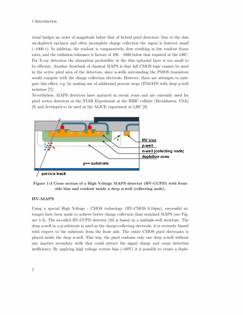
terial budget an order of magnitude below that of hybrid pixel detectors. Due to the thin un-depleted epi-layer and often incomplete charge collection the signal is however small (~1000 e). In addition, the readout is comparatively slow resulting in low readout frame rates, and the radiation tolerance is factors of 100 – 1000 below that required at the LHC. For X-ray detection the absorption probability in the thin epitaxial layer is too small to be efficient. Another drawback of classical MAPS is that full CMOS logic cannot be used in the active pixel area of the detectors, since n-wells surrounding the PMOS transistors would compete with the charge collection electrode. However, there are attempts to miti-gate this effect, e.g. by making use of additional process steps (INMAPS with deep p-well isolation [7]). Nevertheless, MAPS detectors have matured in recent years and are currently used for pixel vertex detectors at the STAR Experiment at the RHIC collider (Brookhaven, USA) [8] and developed to be used at the ALICE experiment at LHC [9].
Figure 1-3 Cross section of a High Voltage MAPS detector (HV-CCPD) with front
side bias and readout inside a deep n-well (collecting node).
HV-MAPS
Using a special High Voltage - CMOS technology (HV-CMOS 0.18µm), successful at-tempts have been made to achieve better charge collection than standard MAPS (see Fig-ure 1-3). The so-called HV-CCPD detector [10] is based on a multiple-well structure. The deep n-well in a p-substrate is used as the charge-collecting electrode; it is reversely biased with respect to the substrate from the front side. The entire CMOS pixel electronics is placed inside the deep n-well. This way, the pixel contains only one deep n-well without any inactive secondary wells that could attract the signal charge and cause detection inefficiency. By applying high voltage reverse bias (>60V) it is possible to create a deple-

tion depth of a few to tens of microns. Charge collection occurs by drift (in the depleted part) and by diffusion. The prototype device has proven to stand much higher particle radiation fluences than MAPS detectors [11], up to about 1015 cm-2. Limitations of this technology still lie in the usage of PMOS transistors: since the electronics is inside the deep n-well, PMOS transistors have to be used with care (if at all) because of the bulk effect induced by the charge collected in the deep n-well.
Depleted Monolithic Active Pixels (DMAPS)
The goal of this thesis is to develop new types of MAPS by combining different features of existing pixel detector concepts, which have so far not yet been accessible with monolithic active pixel technologies (see Figure 1-4). These features most notably are large signal and fast charge collection by drift in a 50µm – 200µm thick depleted layer, the use of PMOS and NMOS transistors in the pixel cell without limitation (full CMOS), and last but not least the implementation in a commercial technology without the need to modify the vendor’s CMOS process. Still, the fabrication requires the use of dedicated silicon wafers with high resistivity, but the vendor’s standard CMOS process line would not have to be changed. This is an important feature with respect to the availability and cost of such a DMAPS pixel detector fabrication, since it relies on a commercial CMOS process with only little or no post-processing (e.g. thinning and backside implantation).
Figure 1-4 Cross section of a depleted MAPS detector with fully depleted bulk with
backside contact where charge is collected by drift.


10
2 Pixel Detectors
Silicon pixel detectors are one of the most important and complex particle detectors, although their size and volume is small compared to others detectors. Their development experienced a fast increase in complexity and innovative features, enabled by the progress of the semiconductor industry in the last decades, which in turn is driven by the consumer market. Detection of ionizing radiation by a reversely biased semiconductor junction was first reported by McKay in 1951 [12]. The fast technology developments in the semiconductor industry allowed great progress also in silicon detectors and made them important tool of modern high-energy physics experiments, scientific applications on earth and beyond, medical imaging, and many other disciplines.
2.1 Principle of operation
In silicon electrical charge carriers generated by ionizing radiation or particles are separated by an electric field and are collected on the electrodes. Because of the absence of free carriers in depleted silicon recombination processes of the generated charges can be avoided.
Figure 2-1 A fully depleted, reversed biased diode with ionized electron-hole pairs along the particle track drifting towards the readout electrodes.
2 Pixel Detectors
11
The moving charges induce current pulses on the electrodes. The time needed to detect the whole signal depends on the drift path length and on the strength of the electric field. Figure 2-1 shows a process of ionization in a depleted volume of a reversely biased diode. Generated charges move towards electrodes which induce electrical signals on both electrodes (positive current is induced on the electrode connected to p-layer, while a negative current is induced on the electrode connected to n-layer). The current induced by moving charges in reversely biased depleted silicon detector is determined by the total number of elementary charges, by their velocity, and by so-called weighting filed , which is measure of the electrostatic coupling between the moving charges and the electrodes of the detector:
∙ ∙ ∙
In a parallel plate configuration with infinite electrodes separated by the distance dtot, the weighting field is equal to 1/dtot and perpendicular to the electrodes. In the case of device with many electrodes with finite size, the weighting filed is more complicated [13].
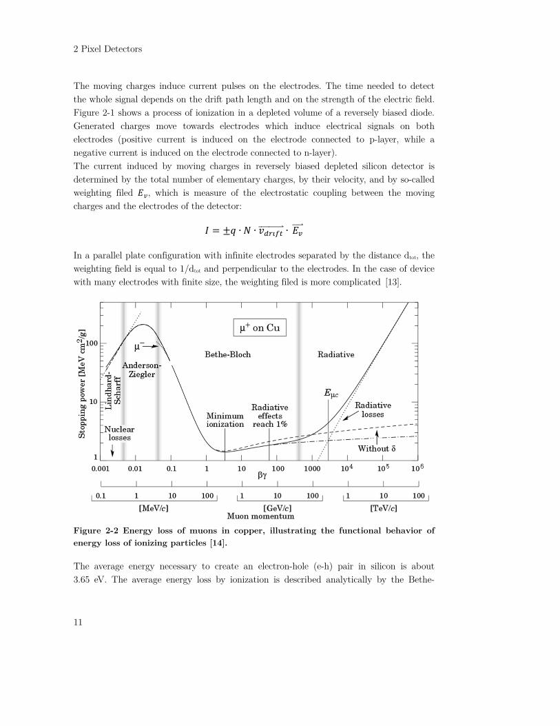
Figure 2-2 Energy loss of muons in copper, illustrating the functional behavior of energy loss of ionizing particles [14].
The average energy necessary to create an electron-hole (e-h) pair in silicon is about 3.65 eV. The average energy loss by ionization is described analytically by the Bethe-
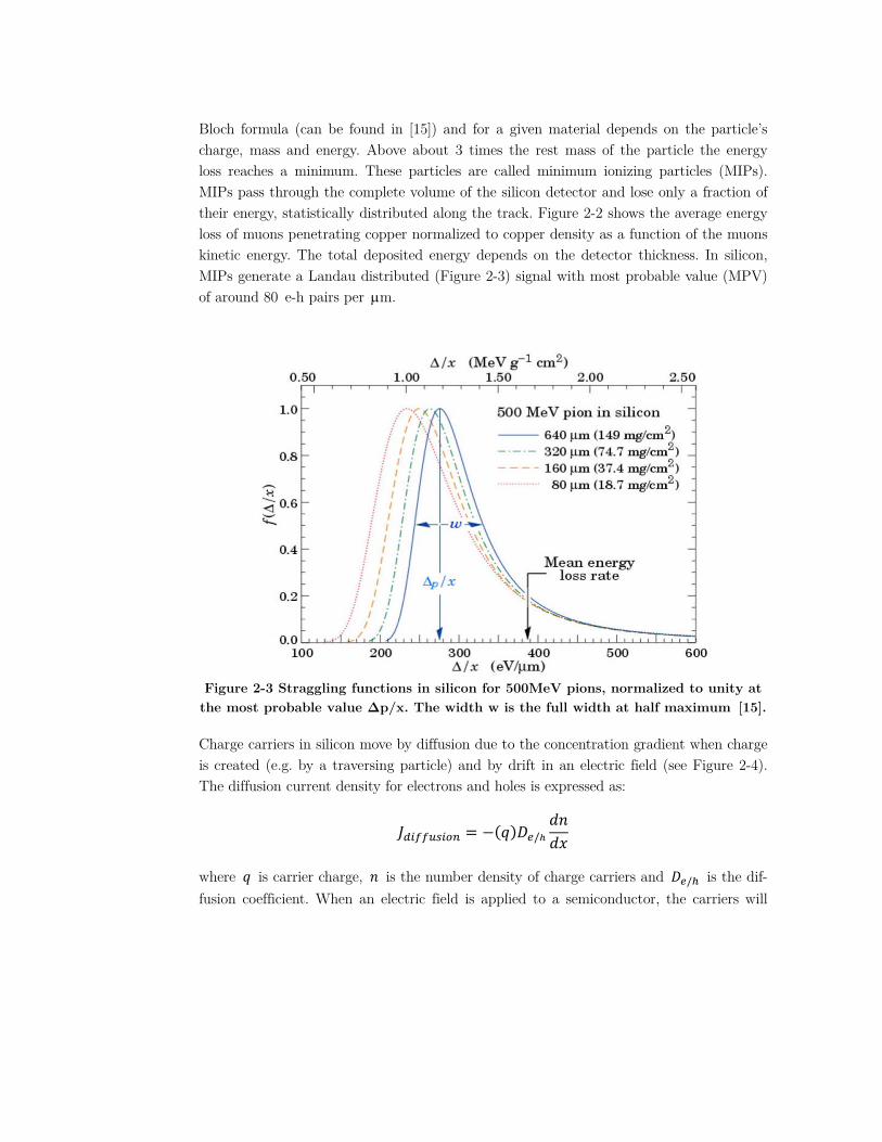
Bloch formula (can be found in [15]) and for a given material depends on the particle’s charge, mass and energy. Above about 3 times the rest mass of the particle the energy loss reaches a minimum. These particles are called minimum ionizing particles (MIPs). MIPs pass through the complete volume of the silicon detector and lose only a fraction of their energy, statistically distributed along the track. Figure 2-2 shows the average energy loss of muons penetrating copper normalized to copper density as a function of the muons kinetic energy. The total deposited energy depends on the detector thickness. In silicon, MIPs generate a Landau distributed (Figure 2-3) signal with most probable value (MPV) of around 80 e-h pairs per m.
Figure 2-3 Straggling functions in silicon for 500MeV pions, normalized to unity at the most probable value Δp/x. The width w is the full width at half maximum [15].
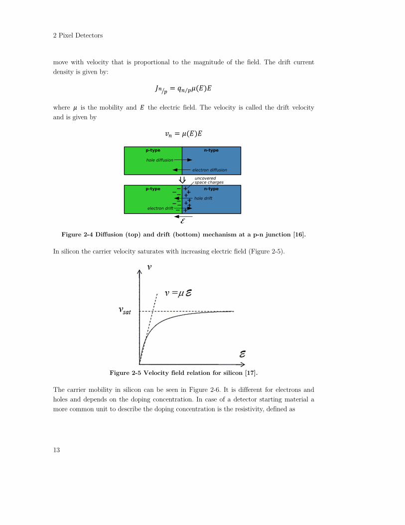
Charge carriers in silicon move by diffusion due to the concentration gradient when charge is created (e.g. by a traversing particle) and by drift in an electric field (see Figure 2-4). The diffusion current density for electrons and holes is expressed as:
/
where is carrier charge, is the number density of charge carriers and / is the dif-fusion coefficient. When an electric field is applied to a semiconductor, the carriers will
2 Pixel Detectors
13
move with velocity that is proportional to the magnitude of the field. The drift current density is given by:
⁄
where is the mobility and the electric field. The velocity is called the drift velocity and is given by
Figure 2-4 Diffusion (top) and drift (bottom) mechanism at a p-n junction [16].
In silicon the carrier velocity saturates with increasing electric field (Figure 2-5).
Figure 2-5 Velocity field relation for silicon [17].
The carrier mobility in silicon can be seen in Figure 2-6. It is different for electrons and holes and depends on the doping concentration. In case of a detector starting material a more common unit to describe the doping concentration is the resistivity, defined as

1
where q is the elementary charge, , and , are the respective mobilities and densities of electrons and holes.
Figure 2-6 Electron and hole (left) mobility (right) resistivity of n-type and p-type
silicon versus doping density [17].
2.2 Readout of pixel detectors
Two readout schemes are used most often in pixel detectors for High Energy Physics (HEP). The first one is a readout using only three transistors in every pixel cell (Figure 2-7.). The readout is column wise in so-called “rolling shutter” mode (see below). This technique is suitable for devices which do not require fast timing information. The other one is based on a charge sensitive amplifier (CSA) front-end and in-pixel discrimination. In this case, often more complex sparsified readout is used. This type of readout is typical for detectors that require precise timing information or have large input capacitance.
Three-transistor pixel readout
One of the simplest and commonly used pixel readout is the so-called three-transistor (3T) design. Because of its simplicity it allows very small pixel size. It consists of the reset transistor, Mrst, that acts as a switch to reset the diode. When Mrst is turned on, the diode is effectively connected to the power supply, VRST, clearing all integrated charges. The read-out transistor, Msf, acts as a buffer (a source follower), which allows the pixel voltage to be measured without removing stored charge. The select transistor, Msel, allows a single row of the pixel array to be read by the read-out electronics. Other varaitions of pixel readout such as 4T, 5T and 6T pixels also exist [18].

2 Pixel Detectors
15
In the case of a 3T pixel cell the charge to voltage conversion takes place on the input capacitance and the voltage output ∆ is proportional to the charge ∆Q on this capacitance :
∆∆Q
The principle of operation is presented on Figure 2-8. Between a periodically applied reset, signal charge is integrated on the input capacitance. Charge deposited in the sensor is measured just before the reset signal appears. In addition a correlated double sampling (CDS) can be used by reading the signal voltage twice, after reset and before next reset and substracting measured voltage.
Figure 2-7 A three-transistor active pixel sensor [18].
The major noise sources for a 3T cell are reset noise (also known as kTC noise) introduced by Mrst, (see Figure 2-7) which originates from random fluctuations in the voltages reading due to reset potential fluctuations and fixed pattern noise that comes from the differences in the components in each pixel producing a static noise pattern. Both, reset noise and fixed pattern noise can be removed by CDS. Other major noise sources are shot noise which is proportional to sensor dark current (leakage) and flicker noise (1/f) including random telegraph noise (RTS) [19].

RESET
OUPUT
SAMPLESAMPLE(CDS)
leakage
signal
particle
Figure 2-8 A three-transistor principle of operation.
Charge Sensing Amplifier Pixel Front-End
The front-end of most readout chips for hybrid pixel sensors consists of a charge sensitive amplifier (CSA) at the input. Figure 2-9 shows a model of a typical CSA consisting of an amplifier, an output buffer and the feedback capacitance.
Figure 2-9 Block diagram of the CSA [20].
A CSA translates charge ∆ to the voltage∆ and consists of a high open loop gain core amplifier and a capacitive feedback . In the ideal case, the CSA behaves as an in-tegrator with a closed loop gain inversely proportional to the feedback capacitance. The output voltage follows the input charge :
∆∆
; 1

2 Pixel Detectors
17
In reality the core amplifier has a finite open loop gain. The capacitance of the sensor can be significantly larger than the feedback capacitance. Taking these effects into ac-count, the formula for the CSA gain changes to:
1
where is the open loop gain of the core amplifier. This suggests that a low detector ca-pacitance and a high open loop gain of the core amplifier is often aimed at.
Figure 2-10 The CSA with different discharge circuits: (a) the CSA with resistive feedback discharges exponentially with time constant f = RfCf (b) the switched feedback CSA discharges within a short reset period when the feedback switch is switched on. (c) the CSA with constant current feedback discharges linearly with
time [20].
Each CSA requires a reset circuit to avoid saturation. The reset can be implemented by a resistor (Figure 2-10 (a)), a switch (Figure 2-10 (b)) or by a current source (Figure 2-10 (c)) connected in the feedback loop of the CSA. These options and corresponding output waveforms are shown in Figure 2-10. To better understand the parameters of the CSA and its consequences let us consider an example of the simplest implementation of an inverting amplifier in CMOS technology (shown in Figure 2-11). The inverting amplifier consists of an NMOS input transistor and a load formed by a PMOS transistor with constant biasing voltage.

Figure 2-11 Inverting amplifier with NMOS input transistor and PMOS load tran-
sistor (left), small-signal equivalent circuit (right) [21].
An important parameter of every CSA is the rise time which has a mayor impact on precision measurement of the time of arrival of a particle. For a simple circuit on Figure 2-11 taking into account that typically ≪ and ≪ , the expression for the rise time can be approximated to [21]:
∶ ≪
∶ ≫
where is input transistor transconductance. Hence for a feedback capacitance larger than the load capacitance the signal rise time is approximately independent of the feedback capacitance , whereas for a feedback capacitance smaller than the load capacitance the signal rise time scales inverse proportional to . Another as important parameter of the CSA is noise. The dominant noise contributions are shot noise from sensor leakage current, as well as thermal and 1/f-noise in the channel of the input transistor. Common measure of noise for detectors readout circuits is equiva-lent noise charge (ENC) which describes fluctuation at the input (in electrons) of the am-plifier that is equivalent to voltage noise at the output.
The total ENC of the CSA is expressed as a quadratic sum of all noise compo-nents:
/
For a simple inverting charge sensitive amplifier the input noise spectra (parallel current noise, serial voltage noise, respectively) and the equivalent noise charge ENC for dominant contributions are [1]: From the leakage current :

2 Pixel Detectors
19
2
where is elementary charge and is amplifier (constant current feedback) output fall time.
From transistor channel noise:
83
23
The expression does not depend on gm because decrease in noise is canceled by increase of bandwidth. The situation is different when bandwidth is limited by following shaper circuit.
From 1/f-noise:
/ /
where is technology-dependent constant, is the gate oxide capacitance and W,L are the effective width and length of the transistor.
For fast pixel detectors before irradiation the dominant noise source typically is thermal noise from the transistor channel, whereas after receiving significant radiation dose the dominant noise source comes from leakage.
Rolling Shutter Readout
The simplest and most typical readout for 3T cells is the rolling shutter readout (see Fig-ure 2-12). In this case all pixel outputs in the column are connected. Only one row of pix-els is selected at a time for readout and/or reset. The column outputs can be multiplexed at the periphery in case of limited analog outputs. The recorded values can be digitized by external or internal components.

Figure 2-12 Rolling shutter readout concept where the integrated signal is read out
and reset row by row.
Sparsified readout architecture
Typical readout electronics for hybrid pixel sensors used in high-energy physics consist of an in-pixel analog front-end with a charge sensitive amplifier directly connected to the sensor part (bump bonds, see Figure 1-1), a comparator with a tunable threshold and a digital logic section with time stamping and storage memory. The digitized analog input and time information can be read immediately out from the pixel, or stored in on-chip memory cells to be read out later triggered by an external trigger signal. A block diagram for a typical sparsified readout chip is shown in Figure 2-13.
Figure 2-13 A typical hybrid pixel readout front-end channel contains charge sensi-
tive amplifier, shaper, discriminator and pixel logic [20].
2 Pixel Detectors
21
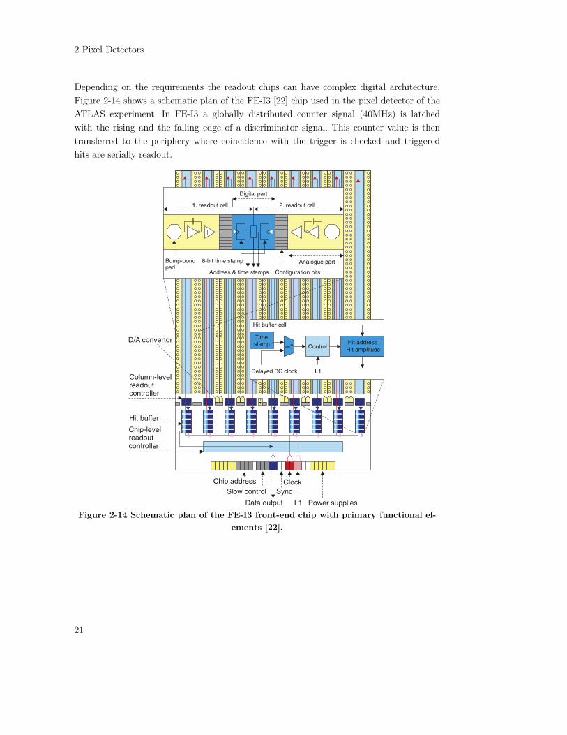
Depending on the requirements the readout chips can have complex digital architecture. Figure 2-14 shows a schematic plan of the FE-I3 [22] chip used in the pixel detector of the ATLAS experiment. In FE-I3 a globally distributed counter signal (40MHz) is latched with the rising and the falling edge of a discriminator signal. This counter value is then transferred to the periphery where coincidence with the trigger is checked and triggered hits are serially readout.
Figure 2-14 Schematic plan of the FE-I3 front-end chip with primary functional el-
ements [22].

2.3 The ATLAS FE-I4 pixel readout chip
FE-I4 [23] is a hybrid pixel readout chip that was designed to cope with the high hit rates expected at the LHC very close (r=3.5cm) to the interaction point. Similar rates are also expected at outer layers (r>25cm) for the planned LHC luminosity upgrade (HL-LHC). Since a fully monolithic sensor (integrating sensor and all readout) is difficult to realize the FE-I4 is also being used a “test vehicle” for the performance investigation of some CMOS pixel detectors (see Chapter 4.2). FE-I4 is designed in 130nm technology (IBM) that allows a high digital design density and radiation tolerance. The pixel array consists of 80x336 pixels of 50x250µm2 area. The readout chip incorporates a new digital and ana-log architecture that helps to lower the detection threshold and reduce the hit losses. It includes on-chip power regulators that allow to decrease a number of external components and to reduce the power losses in the cables. An increased amount of digital logic reduces the need for external processing of the data. The FE-I4 chip was designed to work with planar silicon sensors, 3D sensors [24] and diamond sensors [25]. A more detailed specifi-cation of the FE-I4 chip can found in Table 2-1.
Table 2-1 FE-I4 Pixel Front End chip specification. CMOS Process IBM 130 nm
Chip Size 20 x 19 mm2 Pixel Size 50 x 250 µm2 Array Size 80 x 336 pixels
Supply Voltage (digital/analog) 1.2/1.4 V Analog Power Consumption 14 µW/pixel Digital Power Consumption 6 µW/pixel
Typical CSA Noise 100 e- (at 100fF input) Typical Operating Threshold 3000 e-
ToT Resolution 4 bit CSA Feedback Capacitor 17 fF CSA Return To Baseline 1550 e-/BC
Output Data Rate 160 Mb/s
Figure 2-15 shows the block diagram of the entire FE-I4 chip. The chip consists of an ac-tive part (pixel array) and periphery. The pixel array is organized in 40 double columns (DC). Every DC consists of 2x336 pixels. Pixels in the DC are grouped in four-pixel re-gions. This region has four independent identical analog channels sharing their digital parts were hit processing, storage, triggering and readout take place. Timing and trigger information is distributed globally throughout the chip. The readout is organized in the form of two tokens that allow arbitration of data transferes coming from the pixels. The

2 Pixel Detectors
23
first token exists in every DC, a second one at the periphery of the chip. Transferred data is sorted and processed at the end of chip logic and is later serialized and sent by the data output block. Other peripheral blocks are placed at the bottom of the chip, among them the most essential are phase locked loop, biasing DACs, power regulators, a command decoder and configuration registers. In comparison to FE-I3 the FE-I4 chip can handle much higher hit rate by storing and triggering the hits in the array (locally to the pixel), where in FE-I3 it has to be always transferred to the periphery (limited by on-chip band-width). FE-I4 also has higher output bandwidth of 160Mbit/s (40Mbit/s for FE-I3).
Figure 2-15 Overall block diagram of FE-I4 [21].
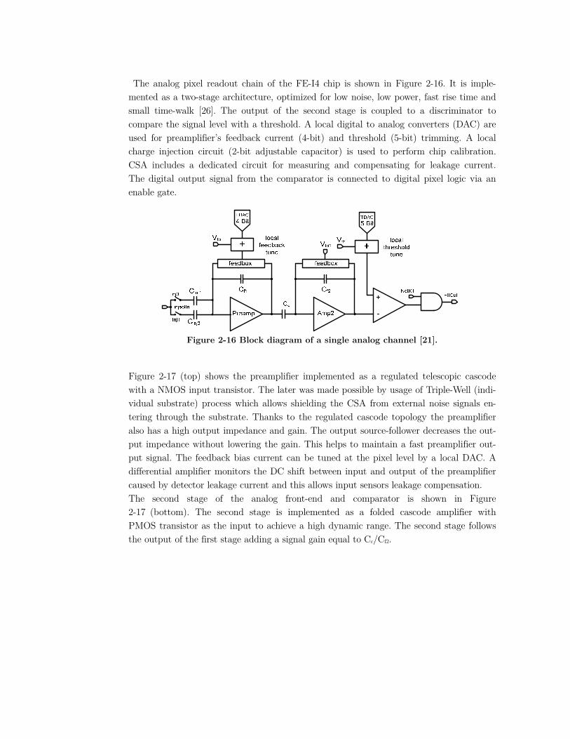
The analog pixel readout chain of the FE-I4 chip is shown in Figure 2-16. It is imple-mented as a two-stage architecture, optimized for low noise, low power, fast rise time and small time-walk [26]. The output of the second stage is coupled to a discriminator to compare the signal level with a threshold. A local digital to analog converters (DAC) are used for preamplifier’s feedback current (4-bit) and threshold (5-bit) trimming. A local charge injection circuit (2-bit adjustable capacitor) is used to perform chip calibration. CSA includes a dedicated circuit for measuring and compensating for leakage current. The digital output signal from the comparator is connected to digital pixel logic via an enable gate.
Figure 2-16 Block diagram of a single analog channel [21].
Figure 2-17 (top) shows the preamplifier implemented as a regulated telescopic cascode with a NMOS input transistor. The later was made possible by usage of Triple-Well (indi-vidual substrate) process which allows shielding the CSA from external noise signals en-tering through the substrate. Thanks to the regulated cascode topology the preamplifier also has a high output impedance and gain. The output source-follower decreases the out-put impedance without lowering the gain. This helps to maintain a fast preamplifier out-put signal. The feedback bias current can be tuned at the pixel level by a local DAC. A differential amplifier monitors the DC shift between input and output of the preamplifier caused by detector leakage current and this allows input sensors leakage compensation. The second stage of the analog front-end and comparator is shown in Figure 2-17 (bottom). The second stage is implemented as a folded cascode amplifier with PMOS transistor as the input to achieve a high dynamic range. The second stage follows the output of the first stage adding a signal gain equal to Cc/Cf2.

2 Pixel Detectors
25
Hit
VDDD
VbnDis
GNDD
Comparator
VthGlobal
Vbp
Vin Vbpsf
Cf2=8.7fF
VbpFB
Vbn
2nd-Stage Threshold Tuning System
VbpMain
R
2R
4R
8R
16R
D0
D1
D2
D3
D4
VbpStep
M1
M2
M3
M4
M5
M6
M7
M8
M9
M10
M11
M12 M13
M14 M15
M16
M17
M18
M20M19
Figure 2-17 Schematic of FE-I4 (top) preamplifier with constant current feedback
and leakage compensation and (bottom) second-stage amplifier with comparator [21].
A sensor signal from a particle crossing the detector can be electrically represented as a fast current signal at the input of preamplifier. Figure 2-18 shows a typical transient re-sponse of the first stage amplifier for different input charges deposited in the sensor. One can observe a characteristic triangular shape with a fast rise time (defining the time coin-cident with the incident particle) and a slow return to baseline. For testing purposes a voltage pulse on a known capacitor is used to inject equivalent sensor charge to the input of preamplifier. Figure 2-19 shows a typical response of the first and the second stage amplifier for voltage pulse applied to the input of preamplifier through 5fF capacitor. The leading (falling) edge of the input pulse injects negative charge. Therefore the ampli-fier response is the same as in the case of signal from the sensor. In case of the voltage

pulse one can observe an artifact at the trailing (rising) edge of the input pulse. This arti-fact can be minimized by reducing the slope of the trailing edge. The amount of charge deposited in the sensor is evaluated by measuring the time it takes to return to baseline (Time over Threshold – ToT). The FE-I4 chip has a limited digital ToT resolution of only 4 bit.
Figure 2-18 Output voltage transients of (top) the first and (bottom) the second
stage amplifier, of FE-I4 as a function of the charge signal which is varied linearly between 5ke- and 25ke- in 5ke- steps.
Figure 2-19 Output voltage transients of (middle) the first and (bottom) second
stage FE-I4 amplifier as a function of the (top) input voltage pulse applied through 5fF capacitor for varied amplitudes.


28
3 Pixel operation environment at LHC
The goal of the particle detector is to provide tracking with precise vertex reconstruction in presence of a strong magnetic field. At the heart of the tracking lies the pixel detector. The main task of this detector is vertex finding and flavor tagging. An efficient tagging of particles requires tracking as close as possible to the primary interaction vertex. The high spatial particle track density close to the interaction point makes it necessary to employ detectors with small pixel size. These provide a fine granularity in three dimen-sions [27]. The different environments of various accelerators and the resulting require-ments on the pixel detector are summarized in Table 3-1.
Table 3-1 Requirements for different existing and planned pixel detectors
ALICE-LHC
ILC BELLE II ATLAS-LHC
ATLAS-HL-LHC
Type heavy-ion e+e- e+e- p+p p+pTiming [ns] 20 000 350 20 000 25 25
Particle Rate [kHz/mm2/s]
10 250 400 1000 10000
Fluence [neq/cm2]
> 1013 1012 ~3x10¹² > 1015 > 1016
Ion. Dose [MRad]
0.7 0.4 1 80 > 500
Material Budget [x/X0 per layer]
1 0.3 0.5 3.5 2?
Power [mW/cm2]
100 100 <200 <500
3.1 LHC
The most technically demanding environment for pixel detectors is the LHC (see Figure 3-1). A long LHC shutdown is planned (LHC Phase 2) after 2025 when the existing pixel detector will be at the end of its lifetime and will be completely replaced. After this up-grade, LHC peak luminosity will reach up to 1035cm-2s-1. This extremely high luminosity poses great challenges on pixel detectors to resolve tracks in jets, resulting in very high hit particle rates interacting with detector (1-3 GHz/cm2 for the inner part), high trigger

3 Pixel operation environment at LHC
29
rates (>1 MHz) and long trigger delay times (>10µs latency) [28]. Those extremely high rates involve massive data processing still inside the detector which leads to high power consumption and puts a high demand on power delivery and cooling. As a consequence large mechanical constructions are needed for cooling. This degrades the resolution due to multiple scattering which is related to the amount of material on the path of particle
/ . The LHC Phase 2 Upgrade introduces unprecedented radiation levels in terms of ionizing dose (>500 MRad for detector lifetime) and particle fluence (> 1016
neq/cm2) as discussed in next section. Typically CMOS submicron technologies can sustain high ioniz-ing dose [28], but the biggest challenge is to cope with bulk damage as a consequence of non-ionizing damage caused by high fluence.
Figure 3-1 Schematic view of the LHC with its experiments. A 27 kilometers tunnel, beneath the French-Swiss border. It is designed to either collide particle beams of
protons at up to 7 TeV per nucleon or lead nuclei [29].
3.2 Radiation Damage
The extremely high radiation environment in which the detector operates requires an in-depth knowledge of radiation effects in order to assess the performance degradation of particle detectors introduced by radiation. The detector environment puts rigorous re-quirements on the radiation hardness of the basic detector components. The tracking de-vices are exposed to large fluences of damaging radiation and have to retain a minimum signal to noise ratio for efficient particle detection. The main effects due to radiation damage can be summarized in two classes: surface damage and bulk damage [30].

3.2.1 Surface damage
Surface damage in silicon is due to the ionization energy loss of charged particles or X-ray photons, which cause charges and traps building up in the SiO2 and at the Si-SiO2 inter-face.
Figure 3-2 Representation of the ionizing radiation damage mechanisms in
SiO2 [31].
The mechanisms of surface damage have been described in [32] [33] [34] [31]. “It is caused by the fact that charged particles or X-rays produce electron-hole pairs in the SiO2. Depending on the strength of the electric field in the SiO2 and the type of incident particles, a fraction of electrons and holes recombines. The remaining electrons and holes escaping from the initial recombination either drift to the electrode or to the Si-SiO2 interface, depending on the direction of the electric field in the SiO2. Some of the holes drifting close to the interface, are captured by oxygen vacancies close to the Si-SiO2 interface and form trapped positive charges in the oxide, called oxide charges. During the transport of holes, some react with hydrogenated oxygen vacancies and result in protons. Those protons, which drift to the interface, break the hydrogenated silicon bonds at the interface and produce dangling silicon bonds, namely interface traps, with energy levels distributed throughout the band gap of silicon”[35]. Figure 3-2 shows the mechanisms of
3 Pixel operation environment at LHC
31
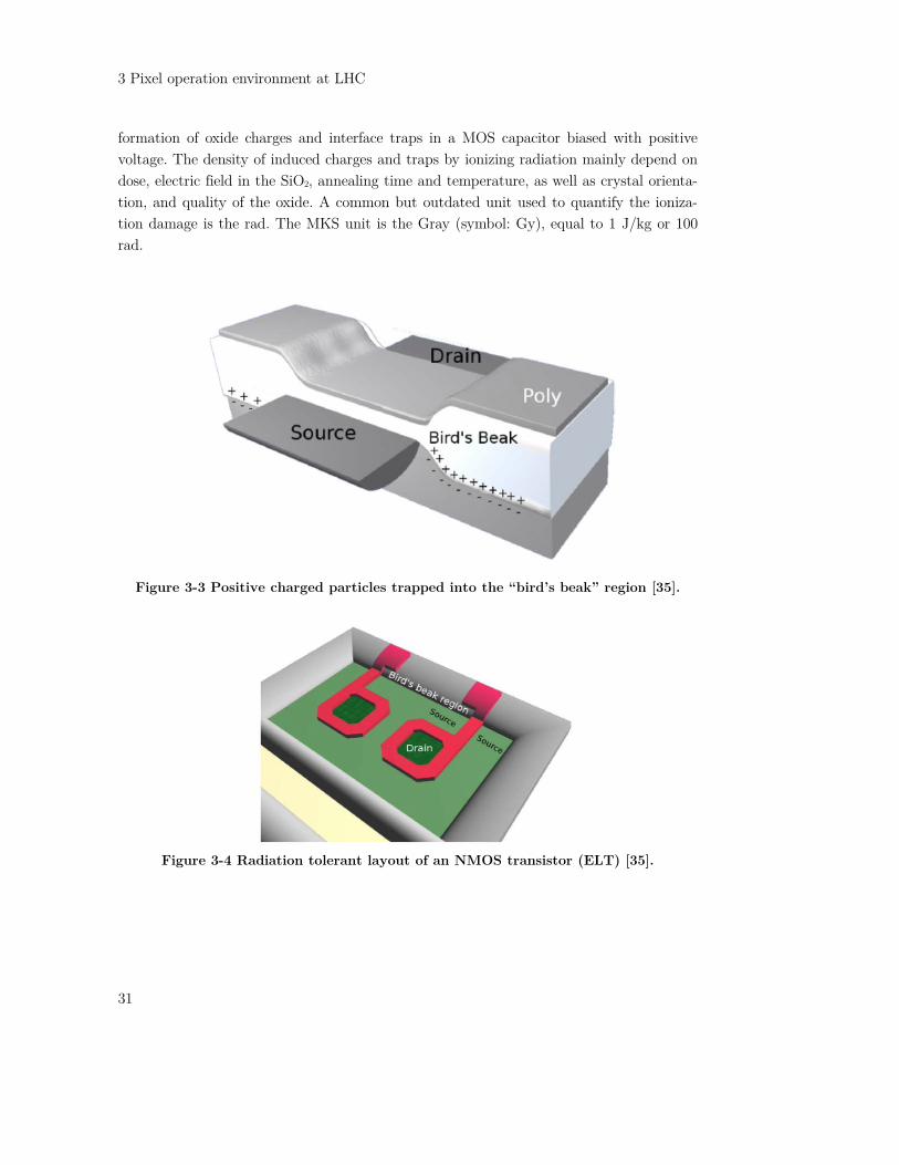
formation of oxide charges and interface traps in a MOS capacitor biased with positive voltage. The density of induced charges and traps by ionizing radiation mainly depend on dose, electric field in the SiO2, annealing time and temperature, as well as crystal orienta-tion, and quality of the oxide. A common but outdated unit used to quantify the ioniza-tion damage is the rad. The MKS unit is the Gray (symbol: Gy), equal to 1 J/kg or 100 rad.
Figure 3-3 Positive charged particles trapped into the “bird’s beak” region [35].
Figure 3-4 Radiation tolerant layout of an NMOS transistor (ELT) [35].
The holes trapped in the deep oxide-traps can be compensated by electron trapping. This can be done either by the thermal excitation of electrons from the valence band (thermal annealing, temperatures up to 300 C) or by the electron tunneling from the silicon sur-face. In deep submicron technologies (where the gate-oxide thickness is below 5 nm) the charge oxide will be removed by tunneling process making those technologies more radiation tolerant to surface damage in the transistor gate area [36]. The elementary electronic device of a CMOS integrated circuit is a MOS field-effect tran-sistor. MOS transistors are sensitive to the radiation induced ionization in the SiO2 layer. We distinguish between two negative effects. One, where the positive trapped charge can induce a parasitic channel between source and drain of a transistor and between contacts of neighboring transistors. The second negative effect is the activation of interface traps which cause the increase of the voltage necessary to switch on a transistor.
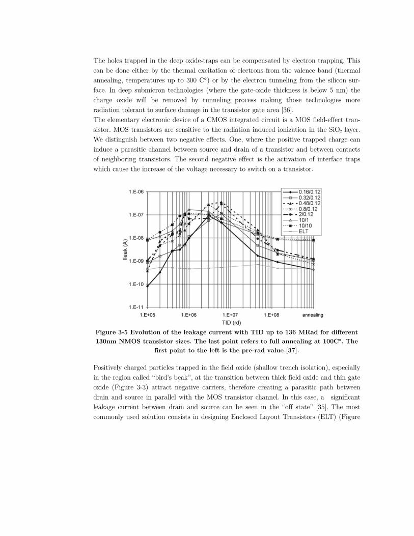
Figure 3-5 Evolution of the leakage current with TID up to 136 MRad for different 130nm NMOS transistor sizes. The last point refers to full annealing at 100C. The
first point to the left is the pre-rad value [37].
Positively charged particles trapped in the field oxide (shallow trench isolation), especially in the region called “bird’s beak”, at the transition between thick field oxide and thin gate oxide (Figure 3-3) attract negative carriers, therefore creating a parasitic path between drain and source in parallel with the MOS transistor channel. In this case, a significant leakage current between drain and source can be seen in the “off state” [35]. The most commonly used solution consists in designing Enclosed Layout Transistors (ELT) (Figure

3 Pixel operation environment at LHC
33
3-4). Figure 3-5 shows leakage current for NMOS transistors for different transistor geom-etries in 130nm technology.
Figure 3-6 Threshold shift with TID up to 136 MRad for different 130nm NMOS
transistor sizes. The last point refers to full annealing at 100C [37].
Normally, threshold shift increases with gate oxide thickness. For thin gate oxide (i.e., for thickness lower than approximately 3-5nm), threshold change is negligible due to tunnel-ing effects. Figure 3-6 shows threshold shift of NMOS transistors in 130nm technology for different geometries. The peak leakage and threshold shift in submicron technologies can be explained by two different effects with different time constants. The built-up of posi-tive trapped charge in field oxide at the transistor edge is fast while the process of for-mation interface states is a slower. In NMOS transistors exist a delay between negative charge trapped in interface states and oxide-trapped charge which leads to rebound effect [37]. Leakage and threshold change for typical submicron-technologies has to be consid-ered during the design process and be appropriately addressed. The only visible consequence of surface damage for the operation of the particle sensors is an increase in leakage current, however in HEP applications it is typically orders of magnitude smaller than the leakage current induced by bulk damage. The design has to be adjusted in a way that the changes in the electric field due to the oxide charges do not influence the sensor performance [1].
3.2.2 Bulk Damage to silicon sensors
On a macroscopic scale, damage in solid state detectors causes are a) an increase of a leakage current (increase in noise), b) a changing in effective doping concentration, c) the

decrease in the amount of collected charge due to the charge carrier trapping and d) the reduction of the carrier’s mobility. All those effects lead to a decrease of the signal and increase of noise [38].
Figure 3-7 Monte Carlo simulation of a recoil-atom track with a primary energy of
50 keV [39]
Bulk damage is most of the time nonreversal interaction of the particles with the nuclei of the lattice atoms. A minimum kinetic energy of 260keV for electrons and 190eV for pro-tons and neutrons is needed to remove silicon atom from its lattice place. Low energy electrons and X-ray photons mostly create point defects (small delivered energy) [1]. In case of high energetic particles enough energy can be delivered to cause multiple defects forming dense clusters of defects (see Figure 3-7). Most of the defects inside the cluster repair because of close distance and only small fraction (2%) are active. Cluster defects have a more profound influence on the performance of silicon sensors. [30]. Changes in sensor performance due to defects depend on their concentration, energy level and the individual electron and hole capture cross-section. To be able to compare radiation damage caused by different particle types and energies a non-ionizing energy loss (NIEL) measure is being used The NIEL-value is given in keVcm2/g and is normalized to damaged caused by 1 MeV neutrons. Figure 3-8 shows the normalized NIEL values as a function of energy. Fluence (Φeq/neq) describes damaged caused by arbitrary particle equivalent to 1MeV neutron [1] [40].

3 Pixel operation environment at LHC
35
Figure 3-8 Non-ionising energy loss for different particles [40].
Defects with deep energy levels near the middle of the band gap can act as recombination/generation centers and are responsible for an increase of the detector leakage current [40]. The increase in leakage current is constant with fluence and does not depend on the starting material (Figure 3-9).
Figure 3-9 Reverse sensor current as a function of fluence for different starting
material type after heat treatment for 80min at 60C [41].

The removal of dopants by formation of complex defects as well as the generation of charged centers changes the effective doping concentration Neff, which is the difference of all donor-like states and all acceptor-like states. Neff can be determined from the full de-pletion voltage using:
| |2
where is the diode thickness, is the permittivity of the silicon and is the electron charge. The full depletion voltage is obtained as the bias voltage where the diode reaches its minimum capacitance. Changes of depletion voltage with irradiation for n-type silicon can be seen in Figure 3-10.
Figure 3-10 Change in the depletion voltage (proportional to the absolute effective
doping concentration) as measured immediately after irradiation [42].
The defects could also act as trapping centers affecting the charge collection efficiency (see Figure 3-11). Traps are typically unoccupied due to the lack of free charge carriers in the depletion region. They can trap a part of the signal charge for extended time and this reduce the signal. Trapping is the primary source of charge loss in very high radiation en-vironment. For imaging applications, it affects signal pulse shape too [1].
3 Pixel operation environment at LHC
37
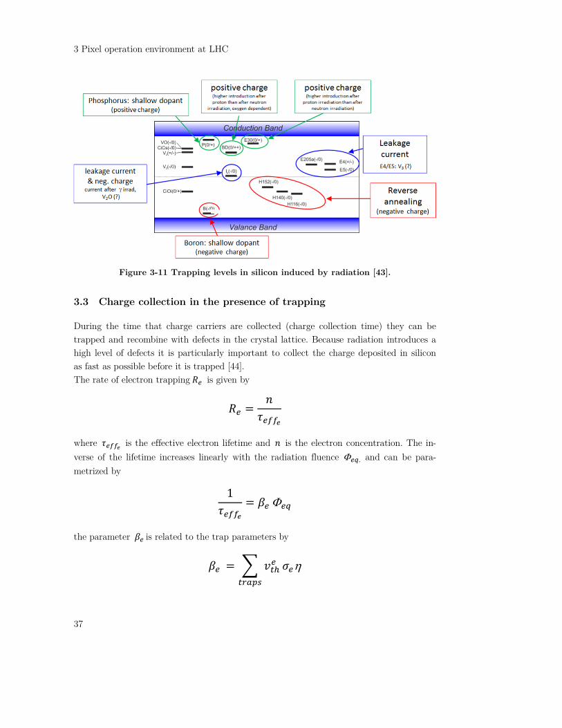
Figure 3-11 Trapping levels in silicon induced by radiation [43].
3.3 Charge collection in the presence of trapping
During the time that charge carriers are collected (charge collection time) they can be trapped and recombine with defects in the crystal lattice. Because radiation introduces a high level of defects it is particularly important to collect the charge deposited in silicon as fast as possible before it is trapped [44]. The rate of electron trapping is given by
where is the effective electron lifetime and is the electron concentration. The in-verse of the lifetime increases linearly with the radiation fluence . and can be para-metrized by
1
the parameter is related to the trap parameters by

where is the electron thermal velocity, the trap cross-section (which reflects the probability of trapping free carriers) and the introduction rate (trap concentrations increase linearly with fluence). Similar equations apply to hole trapping [45].
Simulation example
We consider as an example a simple silicon detector (Figure 3-12). The example detector is based on 18µm p-type epitaxial layer with n-type collecting electrodes separated by p-type regions. Charge collection time and efficiency will be examined for a particle crossing the detector between pixels (worst case, biggest distance to collecting electrodes) for dif-ferent resistivities, bias conditions, radiation levels and ratios of collecting mode area and pitch (fill factor). A simulation package TCAD [46] is used. Trapping levels as given in [47] are used to model radiation effects in the sensor (bulk damage).
Figure 3-12 A cross-section through a silicon detector with epitaxial layer (18um). track of a particle marked as red dashed arrow. A fill factor of 3/20µm is assumed.
Color code is active doping concentration.
Figure 3-13 shows the charge collection for different levels of bulk damage for conditions similar to those of a classical monolithic active sensor where the epitaxial layer resistivity is around 10 Ωcm and about 1 V bias is applied. The low-resistive substrate and the p-type regions are at ground (0V). We observe a fast degradation of the collected charge due to the high level of charge trapping/recombination caused by the slow charge collec-tion (100ns). Figure 3-14 shows charge collection for an increased epitaxial layer resistivity (2kΩcm) and a comparison with a 10Ωcm material. Due to the change in the electrical field distri-bution and increase in mobility the charge collection is faster (10ns). This significantly improves the charge collection efficiency (CCE) for fluences below 1014 neq/cm2.

3 Pixel operation environment at LHC
39
Figure 3-13 Charge collection for the example detector of Figure 3-12 assuming
10Ωcm epi-layer and 1V bias. It can be observed that for classical MAPS detector the charge collection is slow O(100ns) and very fast degrades with fluence.
Figure 3-14 Charge collection for different doses of radiation for the same configura-tion as in Figure 3-12 at 1V bias (left) for an increased epitaxial layer resistivity of 2kΩcm and (right) comparison to 10Ωcm epitaxial layer for fluence of 1013 neq/cm2.
The charge collection for 2kΩcm epi and 20V bias in comparison to 1V bias can be seen in Figure 3-15. As in Figure 3-16 a significant increase of electrical field strength and charge carrier velocity due to higher bias let to a further decrease in the charge collection time and reduces the probability of trapping. In the case of our example detector a signif-icant amount of charge can be collected even after fluences as high as 1015neq/cm2.

Figure 3-15 Charge collection for different fluences for the example detector of Fig-
ure 3-12 with 2kΩcm epi layer at 1 and 20V bias in a function of time.
Figure 3-16 Electron velocity (color coded) for the example detector of Figure 3-12
with 2kΩcm epi layer at (left) 1 and (right) 20V bias
Figure 3-18 shows the influence of the fill factor (area ratio of collecting node to pixel ar-ea) on the charge collection. Figure 3-17 is the resulting electron velocity distribution. The fill factor has a large influence on the CCE especially for particle tracks that traverse in between collecting nodes. In the case of a small fill-factor the electric field is weak at those local areas causing a slower charge collection.
Figure 3-17 Electron velocity (color coded) for an example detector with (left) 25% and (right) 75% fill factor assuming 2kΩcm epi layer and 20V bias at 1014 neq/cm2.

3 Pixel operation environment at LHC
41
Figure 3-18 Charge collection for different fill factor for the example detector with
(left) 10Ωcm (right) 2kΩcm epi layer and 20V bias at 1014 neq/cm2.
For time critical detectors operations like at LHC (25ns time stamping) not only the over-all CCE is important but also fast charge collection which is needed for proper time stamping. If the time stamped for a given pixel hit is less precise than 25ns for all charge values hits can be assigned to wrong collision. Figure 3-19 presents the fraction of charge which has been collected on the example detector for various radiation doses and detector parameters. To achieve high charge collection efficiency for high levels of bulk damage very fast charge collection is needed. To accomplish these, high bias voltage and a high resistive substrate with a large fill factor is required. Additional considerations may need to be taken for an optimal design like the required pixel size, power constraint and signal to noise ratio.
Figure 3-19 A fraction of charge collected in the first 10ns after the interaction from
different levels of radiation and parameters of a detector. It can be observed that according to simulation for high fluence a high bias voltage,high resistivity and large
fill factor are needed.

Influence of backside bias
In all previous examples we have assumed the backside of the sensor to be biased. Figure 3-20 shows comparison of the electron velocity for the example detector (where the thick-ness has been increased to 30µm) with a biased and a floating backside (bias only through p-type implants around pixel/p-stop). As one can observe the electron velocity is substan-tially lower for a floating backside. In consequence the CCE in Figure 3-21 is much worse for unbiased backside before and after radiation. It has to be noted that the situation can be significantly different for different sensor pixel geometry, substrate resistivity, the way the backside was treated during production and other parameters. Backside bias may have a significant influence on the CCE for DMAPS sensors.
Figure 3-20 Electron velocity for an example detector with increased thickens to
30µm (left) biased and (right) unbiased (floating) backside assuming 2kΩcm epi-layer and 20V bias (no radiation).
Figure 3-21 Charge collection for different backside bias scenarios and radiation
doses for 30µm thick example detector with 2kΩcm epi layer and 20V bias.


44
4 DMAPS Implementation and Charac-terization
By looking at a modern CMOS production process that includes high-voltage add-on one can take advantage of existing technology features and exploit them in a nonstandard way such that radiation hard particle detectors can be built. Following chapter present the basic concept and first implementation and characterization of DMAPS devices. This chapter is based on author publications [48] [49] [50] [51] [52] [53] [54] [55] [56] [57] with some passages verbatim copied.
4.1 Design concepts
Two concepts for such depleted CMOS sensors can be distinguished. One (we call it DMAPS A) where the pixel electronics is situated inside the collecting node and a second one (DMAPS B) where the logic is located outside the collecting node. Both approaches have advantages and disadvantages (described below). A third, very attractive option, is to use thick-film High Voltage SOI technology (HV-SOI) where the active electronics is isolated from the sensor part by a buried layer of silicon oxide (BOX).
4.1.1 DMAPS A (read out logic inside collection node)
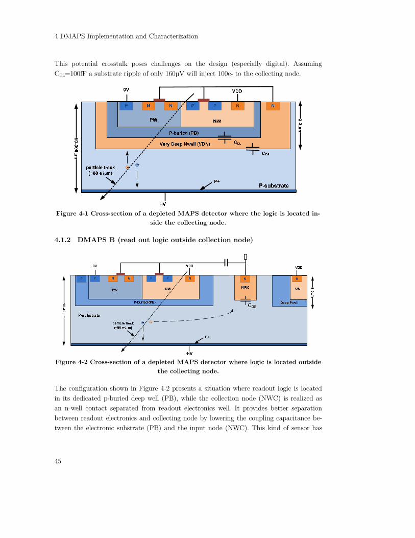
Figure 4-1 shows a cross-section of a depleted DMAPS sensor where the readout logic is located inside the charge collection node. Both PMOS and NMOS transistors are isolated from the n-type collection electrode (very deep n-well - VDN) by a p-buried layer (PB). Apart from the CMOS electronics layer these kinds of sensors are very similar to planar pixel sensors which are completely passive. Their characteristics are a high fill factor and an easy bias (only one backside contact is needed). Therefore it is suitable for operation in high radiation environments. The main disadvantage of such a device is its higher (input) capacitance mainly contributed by the parasitic capacitance (CDL), situated between p-well/p-buried logic substrate potential (PB) and collecting node (VDN). The conse-quence is a higher power demand for the same timing requirement and a worse noise per-formance compared to a passive planar sensor. In addition potential high crosstalk caused by parasitic capacitance (CDL) can be expected. Any activity on the logic substrate will directly be coupled to the most sensitive input node (VDN) through this capacitance.
4 DMAPS Implementation and Characterization
45
This potential crosstalk poses challenges on the design (especially digital). Assuming CDL=100fF a substrate ripple of only 160µV will inject 100e- to the collecting node.
Figure 4-1 Cross-section of a depleted MAPS detector where the logic is located in-
side the collecting node.
4.1.2 DMAPS B (read out logic outside collection node)
Figure 4-2 Cross-section of a depleted MAPS detector where logic is located outside
the collecting node.
The configuration shown in Figure 4-2 presents a situation where readout logic is located in its dedicated p-buried deep well (PB), while the collection node (NWC) is realized as an n-well contact separated from readout electronics well. It provides better separation between readout electronics and collecting node by lowering the coupling capacitance be-tween the electronic substrate (PB) and the input node (NWC). This kind of sensor has
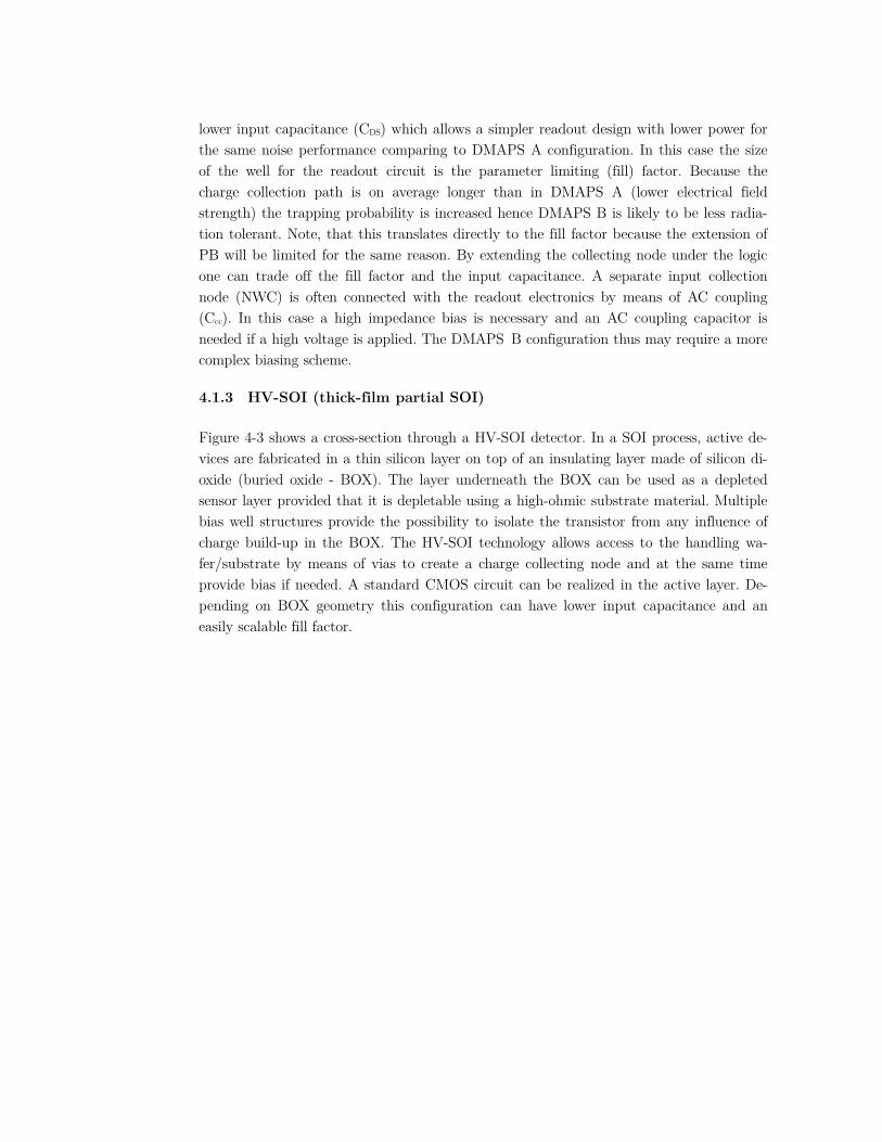
lower input capacitance (CDS) which allows a simpler readout design with lower power for the same noise performance comparing to DMAPS A configuration. In this case the size of the well for the readout circuit is the parameter limiting (fill) factor. Because the charge collection path is on average longer than in DMAPS A (lower electrical field strength) the trapping probability is increased hence DMAPS B is likely to be less radia-tion tolerant. Note, that this translates directly to the fill factor because the extension of PB will be limited for the same reason. By extending the collecting node under the logic one can trade off the fill factor and the input capacitance. A separate input collection node (NWC) is often connected with the readout electronics by means of AC coupling (Ccc). In this case a high impedance bias is necessary and an AC coupling capacitor is needed if a high voltage is applied. The DMAPS B configuration thus may require a more complex biasing scheme.
4.1.3 HV-SOI (thick-film partial SOI)
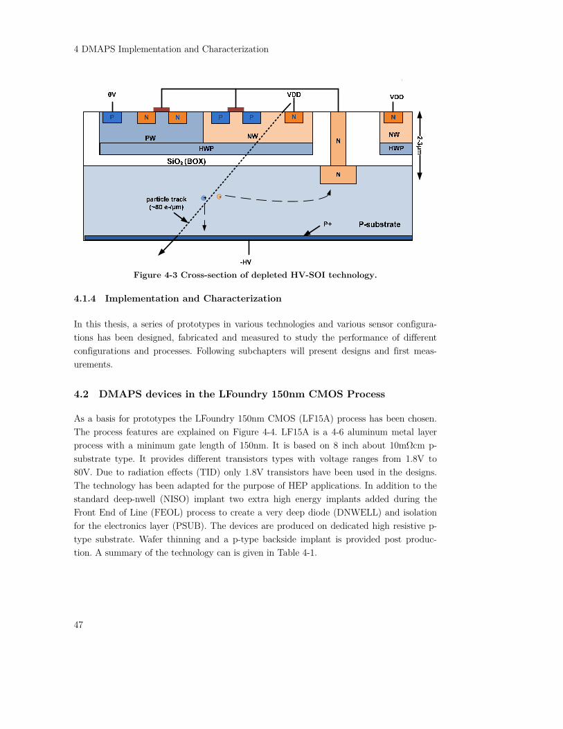
Figure 4-3 shows a cross-section through a HV-SOI detector. In a SOI process, active de-vices are fabricated in a thin silicon layer on top of an insulating layer made of silicon di-oxide (buried oxide - BOX). The layer underneath the BOX can be used as a depleted sensor layer provided that it is depletable using a high-ohmic substrate material. Multiple bias well structures provide the possibility to isolate the transistor from any influence of charge build-up in the BOX. The HV-SOI technology allows access to the handling wa-fer/substrate by means of vias to create a charge collecting node and at the same time provide bias if needed. A standard CMOS circuit can be realized in the active layer. De-pending on BOX geometry this configuration can have lower input capacitance and an easily scalable fill factor.
4 DMAPS Implementation and Characterization
47
Figure 4-3 Cross-section of depleted HV-SOI technology.
4.1.4 Implementation and Characterization
In this thesis, a series of prototypes in various technologies and various sensor configura-tions has been designed, fabricated and measured to study the performance of different configurations and processes. Following subchapters will present designs and first meas-urements.
4.2 DMAPS devices in the LFoundry 150nm CMOS Process
As a basis for prototypes the LFoundry 150nm CMOS (LF15A) process has been chosen. The process features are explained on Figure 4-4. LF15A is a 4-6 aluminum metal layer process with a minimum gate length of 150nm. It is based on 8 inch about 10mΩcm p-substrate type. It provides different transistors types with voltage ranges from 1.8V to 80V. Due to radiation effects (TID) only 1.8V transistors have been used in the designs. The technology has been adapted for the purpose of HEP applications. In addition to the standard deep-nwell (NISO) implant two extra high energy implants added during the Front End of Line (FEOL) process to create a very deep diode (DNWELL) and isolation for the electronics layer (PSUB). The devices are produced on dedicated high resistive p-type substrate. Wafer thinning and a p-type backside implant is provided post produc-tion. A summary of the technology can is given in Table 4-1.

Table 4-1 Overview of technology options for the prototypes based on customized LF15A process.
Feature Property MOS channel length 150 nm
Metals 4-6 layers, Aluminum Supply rail 1.8 V
MOS transistor types low power/regular Wafer type CZ, p-type bulk, >2kOhm-cm
Deep Implants NISO, DNWELL, PSUB
Backside processing Thinning 300µm, p-type implant, an-
nealing, metallization
Figure 4-4 Cros-section view of the LFoundry (LF15A) process [58].
A detailed description of the technology (all CMOS processing steps including implanta-tion, deposition, etching and annealing) is provided by LFoundry which allows detailed technology simulation using Technology Computer Aided Design (TCAD) [46].

4 DMAPS Implementation and Characterization
49
Figure 4-5 Cross-section through the implant structure of a DMAPS A sensor tech-nology in LF15A technology.
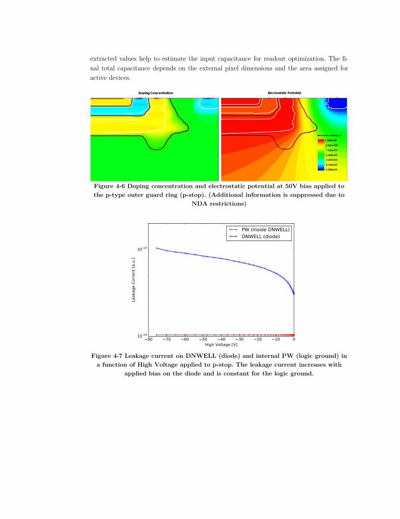
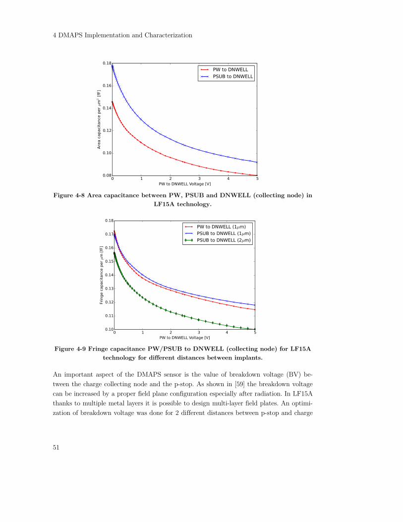
The suitability of the LF15A technology for a DMAPS application is investigated at first in terms of isolation between the logic and the sensor part. The lack of proper isolation may result in a high-voltage potential at the readout part which could damage the tran-sistors. Figure 4-5 shows a cross section through the deep implants of the LF15A technol-ogy. The logic is placed inside the NW and PW wells. The PSUB/PW structure isolates the logic (in the NW) from the collecting node created by a combination of NW/NISO/DNWELL implants. The PW rings (p-stop) around the collection node serve as isolation and to break the accumulation of negative charges at the interface between silicon and silicon oxide layer after irradiation (see Section 3.2.1). Figure 4-6 (left) shows the resulting doping concentration and Figure 4-6 (right) the electrical potential for -50V bias. Bias is applied to the outer p-stop ring (all NW at 2V and PW/PSUB at 0V). As one can observe in Figure 4-7 the structure provides good isolation and the leakage cur-rent into the logic ground (PW/PSUB) is small and does not depend on the sensor bias. An important design parameter to be evaluated for DMAPS sensors is the input capaci-tance. In case of DMAPS A a large part of this capacitance comes from parasitic capaci-tance between the collection node and internal p-well (PW/PSUB). A TCAD simulation has been conducted to estimate this capacitance for the LF15A process. Figure 4-8 shows the extracted area capacitance between DNWELL and PSUB (PW) (see Figure 4-5). As one may expect for a larger distance between PW and DNWELL the capacitance is smaller than between PSUB and DNWELL. The capacitance decreases with higher volt-age due to an increase of the junction depletion zone. For typical bias conditions for this junction (about 2V) the capacitance is about 0.11fF/µm2. Figure 4-9 shows the extracted fringe/edge capacitance between PW/PSUB and NW/NI/DNWELL implants for different distances between them. In all cases the capacitance is in the order of 0.12fF/µm. The
extracted values help to estimate the input capacitance for readout optimization. The fi-nal total capacitance depends on the external pixel dimensions and the area assigned for active devices.
Figure 4-6 Doping concentration and electrostatic potential at 50V bias applied to the p-type outer guard ring (p-stop). (Additional information is suppressed due to
NDA restrictions)
Figure 4-7 Leakage current on DNWELL (diode) and internal PW (logic ground) in
a function of High Voltage applied to p-stop. The leakage current increases with applied bias on the diode and is constant for the logic ground.
4 DMAPS Implementation and Characterization
51
Figure 4-8 Area capacitance between PW, PSUB and DNWELL (collecting node) in
LF15A technology.
Figure 4-9 Fringe capacitance PW/PSUB to DNWELL (collecting node) for LF15A
technology for different distances between implants.
An important aspect of the DMAPS sensor is the value of breakdown voltage (BV) be-tween the charge collecting node and the p-stop. As shown in [59] the breakdown voltage can be increased by a proper field plane configuration especially after radiation. In LF15A thanks to multiple metal layers it is possible to design multi-layer field plates. An optimi-zation of breakdown voltage was done for 2 different distances between p-stop and charge

collecting node (for 6 and 20µm). A TCAD simulation using the Okuto-Crowell impact ionization model [60] has been used to extract the breakdown voltage. A cross section through the simulated structure can be seen in Figure 4-10.
Figure 4-10 Cross-section of a simulated structure to extract the breakdown voltage.
Also visible are the POLY and METAL overhang layer.
To simulate TID effects positive oxide charges have been introduced at the silicon-oxide interface. Figure 4-11 shows the reverse bias current as a function of the reverse voltage for various distances between p-stop and the charge collecting node, the metal and poly overhang and oxide charges at the silicon oxide interface. Simulation indicates that by using proper field plates one can expect a much higher breakdown voltage that increases with distance (d). To understand the influence of field plates one can plot the electric field just below STI (Figure 4-12). It can be observed that adding additional poly/metal field plates allows a smoother distribution of the electrical field between the charge collecting node and p-stop. It also decreases the field maximum.

4 DMAPS Implementation and Characterization
53
Figure 4-11 Leakage current as a function of the bias (HV) voltage for a simulated structure for different distances (d), overhang and oxide charge on the silicon-oxide
interface.
Figure 4-12 Electric field below STI for various overhang and high voltage for 20µm
distance.

Table 4-2 shows a summary of breakdown voltage for different sensor parameters. From simulation one can expect about 150V for 6µm and 300V BV for 20µm distances between diode/n-type implant and p-stop/p-type implant, respectively.
Table 4-2 Breakdown voltages between p-stop and the charge collecting node for different overhang configurations and oxide charges levels on the silicon oxide inter-
face.
Distance [µm]
Poly overhang
[µm]
M1 overhang
[µm]
M2 overhang
[µm]
ox[charges/cm2]
Breakdown [V]
6 0 0 0 1e12 636 2 5 5 1e12 1856 2 5 5 1e10 1486 2 4 6 1e12 1856 1 3 5 1e12 15620 0 0 0 1e12 6420 3 8 13 1e10 30820 3 8 13 1e12 48020 2 5 13 1e12 373
Guard Ring Design
Figure 4-13 shows guard ring distances used for all prototype designs in LF15A. Due to computing time limitations the structure was not simulated in detail but taken from the literature [61]. The 20µm polysilicon and metal overhangs were used for every guard ring.
Figure 4-13 Guard ring structure used for LF15A prototypes [61].

4 DMAPS Implementation and Characterization
55
4.2.1 Diode Test Structures
A set of passive diode test structures has been designed and evaluated for breakdown per-formance and charge collection.
Diode Array A
Diode array A is an array of 5 pixels of 50x250µm2 connected together. Figure 4-14 (left) shows the layout and (right) the pixel cross section through the shorter pixel edge. Figure 4-15 shows the measured diode characteristic. The reverse current stays below 1µA where the diode junction breaks down at a voltage of 110V. This breakdown voltage is three times lower than expected from the simulation (see Table 4-2). This is likely because of the influence on other circuits located on the same die and the modeling precision of the breakdown voltage by TCAD tools.
NW
N
PW(p-stop)
P
POLY
M1
M2
PW(p-stop)
P
POLY
M1
M2
25um
4um
10um
3um
5um
6um
Figure 4-14 Diode array A – with 5 shorted pixels of 50x250µm2 (left) layout of the
diode/pixels and (right) simplified cross section (shorter pixel edge).
Figure 4-15 Reverse current for Diode A (Figure 4-16) in LF15A technology as a
function of bias voltage (300µm thickens, with backside unprocessed).
0 50 100
0.01
0.1
1
10
100
1000
HV [V]
Reverse Curren
t [nA]

Figure 4-17 Scheme of the eTCT setup and the detector connection
scheme [62].
Edge-TCT [63] measurements have been conducted on Diode A. A pulse of infrared light ( = 1064nm, ~1mm attenuation length in silicon) is used to scan the edge of the test structure to study charge collection properties of the diode. The laser light enters into the silicon from the slim edge and this creates charge carriers along its path right below the diode. The TCT setup is shown in Figure 4-17. Figure 4-18 shows the charge collection as a function of the distance/depth (y-axis) from the diode surface for different bias and backside processed structures for different fluence. We observe that at 100V bias a charge from a depth of about 50µm is still collected after 1015neq/cm2. Figure 4-19 shows the charge collection depth as a function of the bias voltage for different fluence. This meas-urement confirms that the wafer resistivity is about 2kΩcm before irradiation and de-creases with fluence. It also shows good charge collection with bias voltage 150V of about 80µm after 1015neq/cm2.
Figure 4-18 Charge vs. depth after different irradiation fluences. (left) the un-
thinned samples without back plane (no BP) and samples with processed back plane (BP) which were thinned to 300 µm. (right) shows charge collection profiles for
samples thinned to 100 µm devices with processed back plane [62].

4 DMAPS Implementation and Characterization
57
Figure 4-19 Edge-TCT of diode array A measurement of charge collection depth in a function of bias voltage for different fluence levels for un-thinned detectors with-
out back plane (no BP) and 300 µm samples with back plane (BP) [62].
Diode Array B
Diode array B is an array of 3x3 pixels of 33x133µm2 connected together. Figure 4-21 shows the layout and the pixel cross section in shorted dimension. Figure 4-15 shows the reverse current.
Figure 4-20 Reverse current for Diode array B in LF15A technology as a function of
bias (thinned 300µm, processed backside).
0 50 100
0.01
0.1
1
10
100
1000
HV [V]
Reverse Curren
t [nA]

PW(p-stop)
P
POLY
M1
PW(p-stop)
P
POLY
M1
33um
3um
3um
4um
6um
PSUB
NW
N
NI
P
DNWELL
NW
N
NI
PW
6um
20um
3um
Figure 4-21 Diode array B – 3x3 connected pixels of 33x125µm2. The layout of the diode/pixels (top), cross section in the direction of the shorter pixel edge (bottom).
Figure 4-22 is the charge drift velocity map obtained from an edge-TCT measurement. Two cases with and without backside processing are shown. The bias voltage is 40V in both cases. One can recognize the 3-pixel-geometry and also an edge effect (red spot) for the outer pixels. In both cases a high drift velocity can be observed up to 100µm from the diode surface. In the backside processed version the velocity distribution is more homogeneous. Due to the positioning of the laser entrance point and its parameters, care has to be taken when comparing Figure 4-22 in absolute scales.
Figure 4-22 Edge-TCT measurement of the charge drift velocity dependent on
distance from diode surface for Diode array B (Figure 4-21) at 40V bias for (left) a 725µm backside unprocessed and (right) 300µm backside processed structure (the
units are relative and the value cannot be compared in absolute terms) [64].

4 DMAPS Implementation and Characterization
59
4.2.2 Passive Planar Sensor
In order to access the performance impact of CMOS pixel sensors with different design features a reference device is employed. This device is a passive CMOS pixel sensor with a pixel footprint compatible to the FE-I4 readout chip (see Section 2.3). It consists of an array of 16x36 pixels (1.8mm x 4mm) with 50x250µm2 pixel area. Every pixel includes a bond pad for the connection to the readout chip. The availability of polysilicon resistors (2kΩ/sq.) and Metal-Isolator-Metal (MIM) capacitors (1fF/µm2) in LF15A technology gives a possibility to include AC coupling circuits in the pixels. This is not possible in traditional planar pixel sensor technologies. AC coupled sensors allow a simplification of the readout because there is no need for a sensor leakage current compensation circuit. Figure 4-23 shows the layout of the sensor and Figure 4-24 a pixel cross section. Half of the matrix (8x36 pixels) includes AC-coupling circuits with 15MΩ polysilicon resistors and 3pF capacitor. The other half is DC-coupled biased using punch through biasing [65] used for sensor testing. Figure 4-25 shows the layout of (left) AC coupled and (bottom) DC coupled pixels for different sizes of the collecting node. Different sizes (fill factor) of the collecting node for the DC-coupled versions are designed to investigate the trade-off between pixel capacitance and the charge collection efficiency.
Figure 4-23 Layout of the passive sensor compatible to FE-I4 readout.
Figure 4-26 shows the breakdown voltage for a 300µm thick backside processed sensor connected to FE-I4 readout chip. The unirradiated sensor breaks down at 170V and >350V after proton radiation. Figure 4-28 shows noise distribution with a mean equiva-lent the noise charge of around 130e- which is the same order as for currently used planar pixel sensors. The slightly higher noise of AC coupled part is due to higher input

capacitance caused by parasitics from biasing capacitor and resistor integrated into the sensor. Figure 4-27 shows sensor efficiency after irradiation in a function of bias voltage for DC and AC-coupled pixels. One can observe that both versions show very good effi-ciency (above 98%) even after fluence of above 1015neq/cm2 and in case of AC-coupled ver-sion above 99.9%. In summary, passive CMOS sensor show good performance in signal, noise level and efficiency similar or better (due to AC coupling) than standard planar sen-sors.
NW
N
PW(p-stop)
P
POLY
M1
M2
PW(p-stop)
P
POLY
M1
M2
BUMP
25um
4um
10um
3um
5um
6um
Figure 4-24 Cross-section of passive sensor (Figure 4-23) across the implant struc-
ture and the metal field plates (50µm side of the pixel).
Figure 4-25 AC (left) and DC-coupled (right) pixel layouts for different flavors of passive planar sensors in LF15A technology with various sizes of the collecting
node.
“p‐stop” polysilicon resistor (~15MΩ)
bump‐pad MIM capacitor (~3pF)
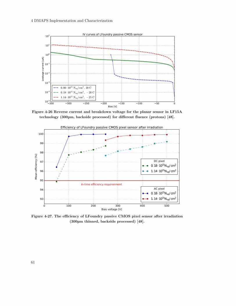
4 DMAPS Implementation and Characterization
61
Figure 4-26 Reverse current and breakdown voltage for the planar sensor in LF15A
technology (300µm, backside processed) for different fluence (protons) [48].
Figure 4-27. The efficiency of LFoundry passive CMOS pixel sensor after irradiation
(300µm thinned, backside processed) [48].

Figure 4-28 Noise map (left) and distribution (right) for a passive sensor in LF15A
technology [48].
4.2.3 CCPD_LF Prototype
The CCPD_LF prototype implemented in LF15A is a follow-up of a series of Capacitive-ly Coupled Pixel Detector designs (CCPD) [66] manufactured on low resistive substrate in AMS 350nm/180nm [11] and Global Foundries 180nm [67] technologies. Previous im-plementations suffer from a shallow (10-20µm) depletion layer and limited use of active CMOS components in the pixel array. Contrary to those designs CCPD_LF for the first time uses high resistive substrate material and allows unrestricted usage of CMOS logic in the pixel array. Two different arrays versions have been designed: CCPD_LF-A and CCPD_LF-B. Figure 4-29 shows the layout of the chips. Both chips consist of a matrix of 24x114 pixels with size 33x125µm2. The major difference between the designs is the sensor layout and biasing.
Figure 4-29 The layout of Capacitively Coupled Pixel Detector in LF15A technology
(left) version A and (right) and B.

4 DMAPS Implementation and Characterization
63
The CCPD concept
An attempt to simplify and reduce time needed to develop fully monolithic prototyping and lower the cost of hybridization during prototype development the CCPD concept has been proposed [66]. Figure 4-30 shows a cross section through a standard hybrid pixel sensor and a CCPD one. In case of the CCPD the connection of the active sensor and the readout electronics is provided by a thin layer of glue. The glue and metal plates on the sensor and on the readout chip create an AC coupling capacitor which is used to transmit the hit information. This solution has been demonstrated to work with different technolo-gies before [11] [67]. The main obstacle of CCPD devices is to keep the glue layer thin, homogenous and well aligned (especially for large devices). Furthermore, electrical signals are needed in addition to the active sensor part (like power and configuration). From an electrical point of view (because of the AC coupled signal) the DC potential on the input node is undefined and can depend on the rate of the transmitted information which can lead to a change of the detection threshold and hence causing nonlinear effects on the re-ceiver side. For CCPD_LF and most of other CCPD-like designs a Front End Chip (FE-I4) is used for the readout of CCPD sensors (see Section 2.3). By connecting more than one CCPD pixel to one and the same receiver of FE-I4 and by encoding the position with ToT value it is possible to obtain better resolution than by a passive sensor approach. One should note that in case of voltage injection is used to transmit hit information between chips, the time, the analog channel is occupied with hit processing (dead time), is increased which can lead to an increase of the hit inefficiency (see Figure 2-19).
Figure 4-30 Standard hybrid pixel-detector with a passive sensor (left) and Capaci-
tive-coupled pixel-detector (right) with active pixel sensor(SCSA) and readout (RCSA) [66].

Design
For CPPD_LF, two sensor architectures A and B were implemented as shown in Figure 4-31. In both cases the charges created in the substrate by a particle are collected by an N-type well (DNWELL). Due to differences in biasing schemes, the two sensors are sepa-rate chips (5mm×5mm). In both cases the pixel size is 33x125µm2 organized in a 24x114 pixel matrix. The pixels are organized in group of six. Each pixel group has an area equal to a group of 2 FE-I4 pixels, so that the FE-I4 pixel receives the output of 3 CCPD_LF pixels. The main difference between the two sensor versions is the size of the charge collecting well, which is about twice bigger in version A, which translates into higher input capaci-tance of the readout electronics. It is expected that version B will exhibit a lower readout noise and its charge sensitive amplifier will have a faster rise time (see Section 2.2). A smaller area of collection electrode means a lower fill factor and possible lower charge col-lection efficiency for an irradiated sensor.
Figure 4-31 Cross-sections and top views of CCPD_LF sensors a) version A: large area for collection and large capacitance b) version B: reduced area and capaci-
tance [49].

4 DMAPS Implementation and Characterization
65
Different bias circuits have been implemented as shown on Figure 4-32. In version A the diode is connected to a transistor based bias circuit, the negative HV potential is applied to the chip substrate/backside. This design is identical to that previously used in CCPD chips. For version B, two flavors of bias are implemented, a diode and a resistor bias. A positive high voltage is applied and the DNWELL to deplete the sensor. In all cases the collecting node is AC coupled to the pre-amplifier and the HV is limited by the break-down of the AC coupling capacitor.
Figure 4-32 Collecting node bias schematic for (a) version A and (b,c) version B of
CCPD_LF.
Figure 4-33 (a) presents a simplified block diagram of the readout electronics inside one pixel. The CSA (shown in Figure 4-33 (b)) is a folded cascode amplifier with adjustable constant current feedback. The feedback capacitor is 5fF. The amplified signal is sent through a coupling capacitor (allow for baseline adjustment) to an input of a discrimina-tor. A schematic of the implemented discriminator (two stage open loop architecture) is presented in Figure 4-33 (c). The discriminator’s threshold can be adjusted locally using a 4-bit trim DAC to reduce the threshold dispersion. A typical current consumption of a pixel is about 15µA. The pixel has two different modes of operation. The standalone mode where hit infor-mation from the discriminator is stored in a flip-flop and later read out via a global shift register. This functionality allows independent operation of the sensor without the readout chip. The second CPPD mode is used in case of a readout chip bonded by either glue or bump bonds. The digital signal from the discriminator can be stretched and its amplitude can be adjusted. A signal processed this way is transmitted through a coupling capacitor to a bond pad. This signal can be optionally connected to an external monitor line.

Figure 4-33 In-pixel electronics of CCPD_LF prototype matrices [49].
Figure 4-34 shows the pixel organization in a group of 6 pixels. Tree pixels outputs are connected to one FE-I4 input. The height of the injection pulse can be controlled individ-ually within a group of three which allows encoding of the pixel position by charge infor-mation (ToT) on the readout chip (Figure 4-35). The pixels are arranged geometrically in a way that allows easier position identification.
Figure 4-34 6-pixel pixel connection to the plates in CCPD_LF(three pixels share
one output).
250µm
100µm

4 DMAPS Implementation and Characterization
67
Figure 4-35 Block diagram of the readout circuitry of the CCPD_LF chip attached to the FE-I4 readout chip. Three pixels of the CCPD_LF chip are connected to one
pixel of the FE-I4 chip. Waveforms of the top pixel (Pix1), middle pixel (Pix2), bottom pixel (Pix3) at each point are shown in blue, green and red,
respectively [50].
Various flavors of in-pixel electronics have been implemented with small differences be-tween them. In version A three different lengths of the CSA feedback loop transistor are used. In version B there are twelve-pixel flavors. The differences between them include the length of the transistor in the CSA feedback loop, sensor bias (through a diode or a resis-tor) and the amount of deep P-well (PSUB) in the pixels. The distribution of the pixel flavors in the matrices is shown in Figure 4-36. Figure 4-37 shows an example transient response of the pixel at the output of the amplifi-er, comparator, pulse width adjustment and input to FE-I4 for different input charges. The signal after adjustment is transmitted to the readout chip via coupling capacitance. Table 4-3 shows results of an example simulation with values for noise and peaking time for different technology corners. Typical noise of about 120e- ENC and peaking time of 30ns are achieved. With such noise figures it is expected that a threshold of about 1000e- can be used. The in-pixel configuration and readout circuitry is shown on Figure 4-38. It consists of a shift register that can be configured to latch and read back the hit information from the comparator or to configure seven latches that store trimming bits, preamplifier enable, injection enable and monitor enable bits.

Figure 4-36 Pixel flavor distribution in version A and B matrices [49].
Figure 4-37 Output transients voltage of the output of (a) CSA , (b) the
comparator, (c) width adjustment circuit and (d) output to readout chip for different charge varied linearly between 2 ke- and 8 ke- in 2 ke- steps (version A,
Lfedback=0.9µm, Cinput=150fF).
a) b) c) d)

4 DMAPS Implementation and Characterization
69
Table 4-3 Noise and peaking time for the schematic simulation for the CCPD_LF prototype (version A, Lfedback=0.9µm, Cinput=150fF). The abbreviation FF,.. SS de-note NMOS and PMOS transistor parameter spreads (fast, slow) representing the
process corners. Process Corner Noise [e- ENC] Peaking Time [ns]
FF 132 26.2FS 136 33.1SF 122 35.5SS 127 30
TYP 128 27.9 Figure 4-39 shows the overall block diagram of the CCPD_LF chip with the pixel matrix. Row control is located on the left side of the matrix, and the periphery is at the bottom. The periphery block consists of global configuration, bias DACs that generate the needed currents for the analog part of the pixel and IO block. In both versions of the chip extra test structures are located at the top of the chip, for example simple transistors to meas-ure radiation effects.
Figure 4-38 In pixel digital configuration and readback for the CCPD_LF proto-
types.
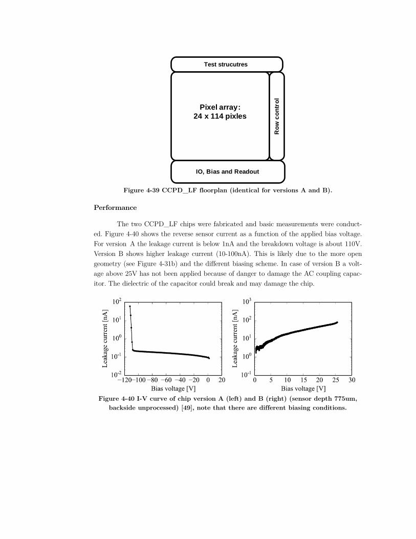
Pixel array:24 x 114 pixles
IO, Bias and Readout
Ro
w c
on
tro
l
Test strucutres
Figure 4-39 CCPD_LF floorplan (identical for versions A and B).
Performance
The two CCPD_LF chips were fabricated and basic measurements were conduct-ed. Figure 4-40 shows the reverse sensor current as a function of the applied bias voltage. For version A the leakage current is below 1nA and the breakdown voltage is about 110V. Version B shows higher leakage current (10-100nA). This is likely due to the more open geometry (see Figure 4-31b) and the different biasing scheme. In case of version B a volt-age above 25V has not been applied because of danger to damage the AC coupling capac-itor. The dielectric of the capacitor could break and may damage the chip.
Figure 4-40 I-V curve of chip version A (left) and B (right) (sensor depth 775um,
backside unprocessed) [49], note that there are different biasing conditions.

4 DMAPS Implementation and Characterization
71
Figure 4-41 shows the single pixel baseline and 55Fe source spectrum measured directly at the output of the preamplifier (buffered). The 5.9 keV Kα peak from the source is ob-served at 10.2 mV (version A) and 13.5 mV (version B) which corresponds to 6.2µV/e- and 7.9µV/e- respectively. The noise is 149e- for version A and 129e- for version B. This is in agreement with simulation.
Figure 4-41 Single pixel baseline (red) and 55Fe source spectrum for the CCPD_LF (left) version A and (right) version B, measured at the (buffered) preamplifier out-
put [49].
The noise values were extracted by multiple charge injection and by varying the global threshold value. Figure 4-42 shows the noise distribution maps. No significant noise inhomogeneities are observed in version A. Version B however shows differences in the noise map, most likely related to its higher input capacitance due to layout differences (see Figure 4-31).
Figure 4-42 Equivalent noise (ENC) maps for CCPD_LF (left) version A and
(right) version B.

To estimate the charge collection distance (CCD), single pixel spectra obtained using a 3.2 GeV electron beam [68] were measured for different bias conditions (Figure 4-43). Based on this a charge collection depths of about 170 µm for version A (at 110V) and about 85 µm for version B (at 20V) are estimated (assuming 80e- charge per µm).
Figure 4-43 Single charge spectra (3.2 GeV electron) of the CCPD_LF sensor for (left) version A and (right) Version B for different bias voltage. (775µm, backside
unprocessed) [51].
To examine the effects of ionizing radiation (TID) on the electronics the chip has been irradiated with 60keV X-rays. The irradiations have been performed at room temperature up to a TID of 50Mrad in several steps. Figure 4-44 shows the normalized gain and the noise changes as a function of TID. One can observe that the gain drops to about 60-80% of its initial value at about 10MRad and recovers to 80-90% at 50Mrad. The noise in-creases up to 180% of the original value. The smallest changes are for an enclosed transis-tor layout. Generally, the TID negatively influences the performance of the electronics but the change is not large and can be properly accounted for in future designs.

4 DMAPS Implementation and Characterization
73
Figure 4-44 Normalized change of (top) gain and (bottom) noise of CCPD_LF (ver-
sion A) as a function of the total ionizing dose. Different colors indicate different types of preamplifier feedback transistor used in the pixel [50].
One of the biggest concerns in this type of sensor is noise coupling from the electronic part to the collecting node (preamplifier input see, Section 4.1.1). In the CCPD_LF this phenomenon is observed and strongly limits the testing capabilities of the chip. As de-scribed before the independent readout is done by a long shift register. Hit information for every pixel can be recorded and serially read out (see Figure 4-38). To switch between hit recording and readout mode a global signal shift-register-enable (SR_EN) is used. Figure 4-45 shows a screenshot from an oscilloscope, where one can observe the monitor output from the comparator (MONOUT) and the amplifier output (AMPOUT) during SR_EN switching. A very strong response of the preamplifier is seen which suggests a large cross-talk noise injection from the switching of the SR_EN signal. The situation is substantially better for version B due to a different layout and a smaller coupling capacitance.

Figure 4-45 Oscilloscope screenshot showing the influence of switching the global
shift-register-enable (SR_EN) signal at the preamplifier output (AMPOUT, CCPD_LF version A).
Conclusions
LF15A is one of the first designs dedicated for HEP applications where DMAPS concepts have been implemented. It is the first time that the CCPD concept was demon-strated using a high-resistive substrate with unrestricted use of CMOS logic inside the pixel and with backside wafer processing. The first sensor results are very promising. Breakdown voltages above 160V is achievable with low leakage currents. This allows achieving more than 200µm of depletion depth in a sensor which at the same time in-cludes full CMOS logic. The performance of the logic is not affected by the sensor and is consistent with the simulation models. First radiation measurements indicate that the process is fairly insensitive to high ionizing radiation doses (both logic and sensor). First studies indicated high tolerance to non-ionizing (NIEL) radiation.
SR_EN
MONOUT
AMPOUT
4µs
170 mV
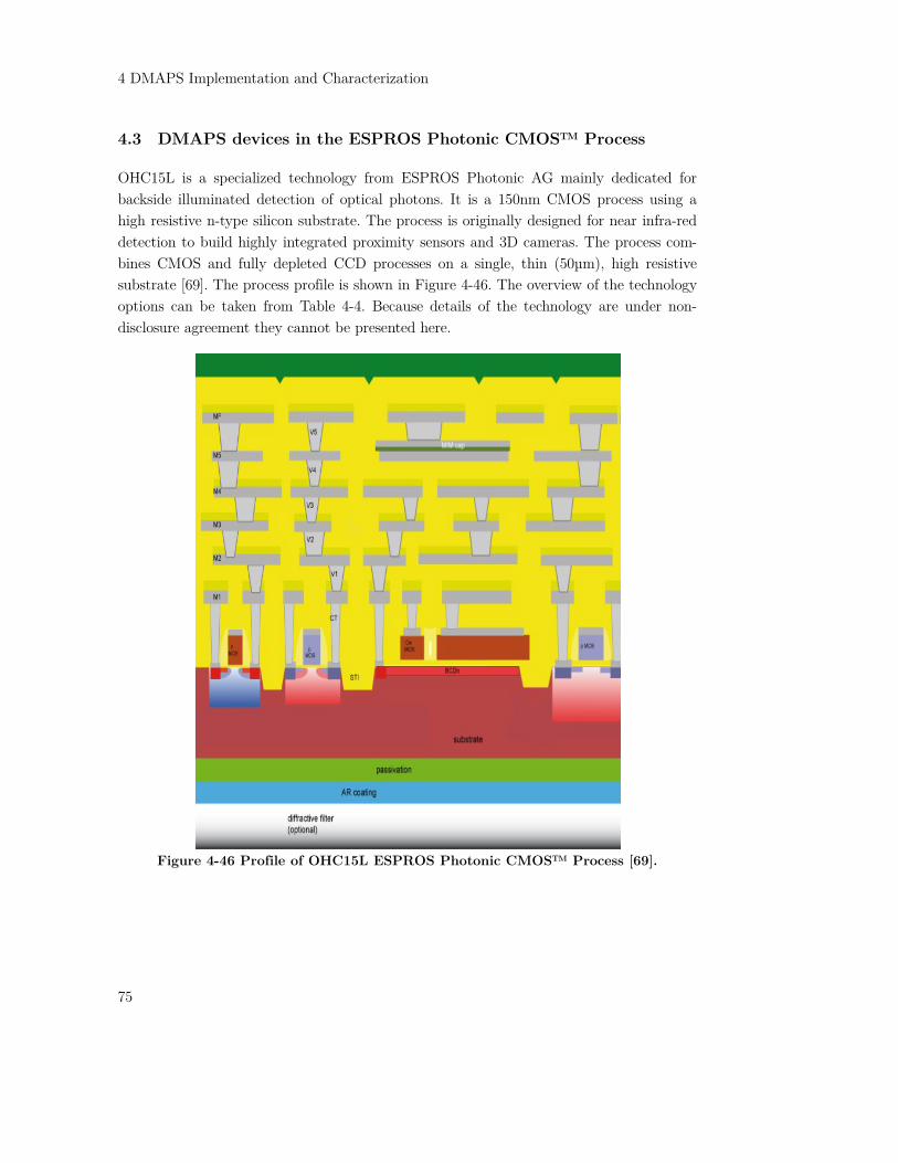
4 DMAPS Implementation and Characterization
75
4.3 DMAPS devices in the ESPROS Photonic CMOS™ Process
OHC15L is a specialized technology from ESPROS Photonic AG mainly dedicated for backside illuminated detection of optical photons. It is a 150nm CMOS process using a high resistive n-type silicon substrate. The process is originally designed for near infra-red detection to build highly integrated proximity sensors and 3D cameras. The process com-bines CMOS and fully depleted CCD processes on a single, thin (50µm), high resistive substrate [69]. The process profile is shown in Figure 4-46. The overview of the technology options can be taken from Table 4-4. Because details of the technology are under non-disclosure agreement they cannot be presented here.
Figure 4-46 Profile of OHC15L ESPROS Photonic CMOS™ Process [69].
Table 4-4 Overview of technology options for the DMAPS prototypes based on the OHC15L process.
Feature Property MOS channel length 150nm
Metals 6 layers, Aluminum Supply rail 1.8 V (5V,12V)
MOS transistor types low power/regular Wafer type n-type bulk, hi-resistive
Deep Implants deep n-well, deep p-well Backside processing thinning 50µm, back implantation
Figure 4-47 shows a typical cross section through the deep implant structure of the OHC15L technology. A deep p-well is implanted in the n-type high resistivity substrate forming a local, isolated p-substrate for the integration of the CMOS electronics. Transis-tors are contained within the deep n-well which allows setting the p-substrate potential independently of the active logic ground potential. The charge collecting node is imple-mented by the n-well implanted directly into the n-type substrate (n-in-n sensor).
Figure 4-47 A cross-section through the implant structure of a DMAPS sensor in
OHC15L technology.
The depletion region grows between the deep p-well and the backside p+ contact poten-tials. Note that two junctions exist, deep p-well/n-substrate and n-substrate/p+backside. This technology allows to bias the n-well (charge collecting node) with high voltage, while the CMOS logic operates at 1.8 V. The n-well electrode collects electrons. The signal of a fully depleted sensor is approximately 4000 e- if a minimum ionizing particle (MIP) cross-es the device. The advantages of this type of sensor are low depletion voltage and a small sensor capacitance.
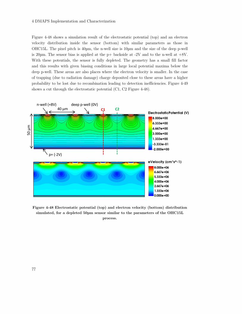
4 DMAPS Implementation and Characterization
77
Figure 4-48 shows a simulation result of the electrostatic potential (top) and an electron velocity distribution inside the sensor (bottom) with similar parameters as those in OHC15L. The pixel pitch is 40µm, the n-well size is 10µm and the size of the deep p-well is 20µm. The sensor bias is applied at the p+ backside at -2V and to the n-well at +8V. With these potentials, the sensor is fully depleted. The geometry has a small fill factor and this results with given biasing conditions in large local potential maxima below the deep p-well. These areas are also places where the electron velocity is smaller. In the case of trapping (due to radiation damage) charge deposited close to these areas have a higher probability to be lost due to recombination leading to detection inefficiencies. Figure 4-49 shows a cut through the electrostatic potential (C1, C2 Figure 4-48).
Figure 4-48 Electrostatic potential (top) and electron velocity (bottom) distribution simulated, for a depleted 50µm sensor similar to the parameters of the OHC15L
process.
50 µm
40 µm n‐well (+8V) deep p‐well (0V)
p+ (‐2V)
C1 C2
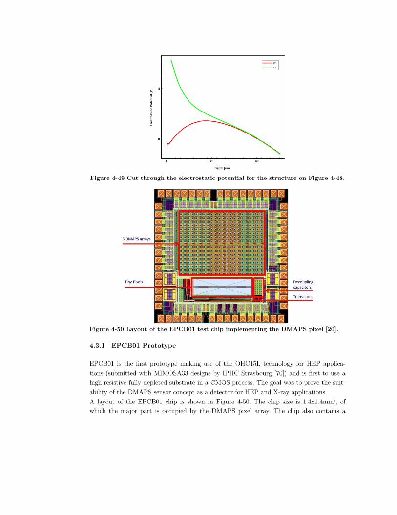
Figure 4-49 Cut through the electrostatic potential for the structure on Figure 4-48.
Figure 4-50 Layout of the EPCB01 test chip implementing the DMAPS pixel [20].
4.3.1 EPCB01 Prototype
EPCB01 is the first prototype making use of the OHC15L technology for HEP applica-tions (submitted with MIMOSA33 designs by IPHC Strasbourg [70]) and is first to use a high-resistive fully depleted substrate in a CMOS process. The goal was to prove the suit-ability of the DMAPS sensor concept as a detector for HEP and X-ray applications. A layout of the EPCB01 chip is shown in Figure 4-50. The chip size is 1.4x1.4mm2, of which the major part is occupied by the DMAPS pixel array. The chip also contains a
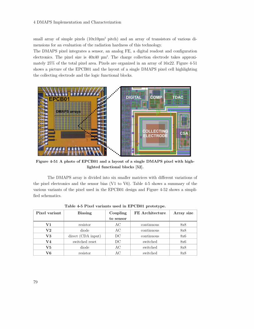
4 DMAPS Implementation and Characterization
79
small array of simple pixels (10x10µm2 pitch) and an array of transistors of various di-mensions for an evaluation of the radiation hardness of this technology. The DMAPS pixel integrates a sensor, an analog FE, a digital readout and configuration electronics. The pixel size is 40x40 µm2. The charge collection electrode takes approxi-mately 25% of the total pixel area. Pixels are organized in an array of 16x22. Figure 4-51 shows a picture of the EPCB01 and the layout of a single DMAPS pixel cell highlighting the collecting electrode and the logic functional blocks.
Figure 4-51 A photo of EPCB01 and a layout of a single DMAPS pixel with high-
lighted functional blocks [52].
The DMAPS array is divided into six smaller matrices with different variations of the pixel electronics and the sensor bias (V1 to V6). Table 4-5 shows a summary of the various variants of the pixel used in the EPCB01 design and Figure 4-52 shows a simpli-fied schematics.
Table 4-5 Pixel variants used in EPCB01 prototype.
Pixel variant Biasing Couplingto sensor
FE Architecture Array size
V1 resistor AC continuous 8x8 V2 diode AC continuous 8x8 V3 direct (CDA input) DC continuous 8x6 V4 switched reset DC switched 8x6 V5 diode AC switched 8x8 V6 resistor AC switched 8x8

In order to study different bias configurations (electrical field inside the sensor) different types of the pixel bias circuits have been implemented. One of them is a DC coupled versions (Figure 4-52 (c) and (d)) where the collecting node is biased directly by the input of the preamplifier. In this case one cannot control the potential of the collect-ing node. The other is an AC-coupled version diode (Figure 4-52 (a),(b),(e) and (f) ) where the collecting node is connected through an AC-coupled capacitor and the bias to the collecting node is provided via a forward biased diode or via a resistor. The AC-coupling allows control of the collecting node potential and to remove a potential DC current (leakage) from the preamplifier which can lead to a performance degradation. In case of AC-coupling the charge seen by the preamplifier input may depend on the value of the coupling capacitor (capacitive divider). An AC-coupling capacitor also adds extra parasitic capacitance to the input of the preamplifier. In case of the bias diode (Figure 4-52 (b) and (e) ) an additional capacitance is very small (small p+ contact in n-well) but the effective resistance is nonlinear with the leakage current and may result in increased noise and nonlinear effects.
To evaluate the performance and suitability for various applications, different ver-sions of the preamplifier feedback have been used. The constant current feedback (Figure 4-52 (a), (b) and (c)) and the clocked reset (Figure 4-52 (e), (d) and (f)) provide that the preamplifier is discharged at a fixed moment of time by a switch.
Figure 4-52 Simplified schematic of different variants of pixels in EPCB01 proto-
type [20].

4 DMAPS Implementation and Characterization
81
Figure 4-53 Schematic diagram of version V2 of the preamplifier and comparator
stages of the EPCB01 prototype.
Figure 4-53 shows the schematic diagram of the FE design for version V2. The preamplifier is a simple common source amplifier with a constant current feedback. No explicit feedback capacitance is used, only the parasitic capacitance. The input of the pre-amplifier is AC-coupled to the collecting node where the diode is used for bias. The out-put signal of the preamplifier is connected to a simple differential comparator with tunable threshold. The configuration and read back is the same as in the case of an inde-pendent readout of the CCPD_LF chip (see Figure 4-38).
Performance
Figure 4-54 shows measurements of the EPCB01 single pixel response to 90Sr and 55Fe ra-dioactive sources. The typical triangular shape response of a continuous current feedback CSA can be observed. At first the performance of the FE electronics is investigated. Figure 4-55 shows the gain of the FE electronics as a function of the injected charge. Each point represents a mean gain of all pixels of the same variant and its standard deviation of the gain variation from pixel to pixel. The error bars have been down-sized by a factor of 2 to keep the graph readable. The highest gain of 99.8 µV/e- measured after the injection of 1 ke- (typical operating threshold) has been achieved with the pixel matrix V2 [52].
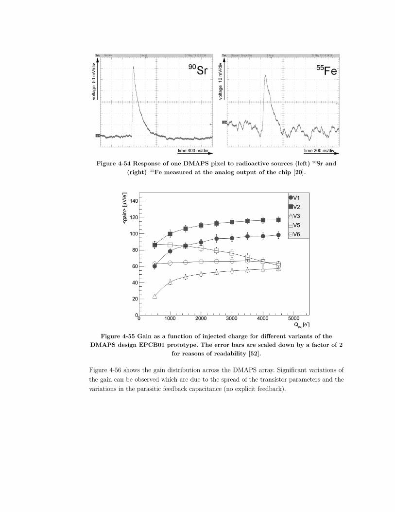
Figure 4-54 Response of one DMAPS pixel to radioactive sources (left) 90Sr and
(right) 55Fe measured at the analog output of the chip [20].
Figure 4-55 Gain as a function of injected charge for different variants of the
DMAPS design EPCB01 prototype. The error bars are scaled down by a factor of 2 for reasons of readability [52].
Figure 4-56 shows the gain distribution across the DMAPS array. Significant variations of the gain can be observed which are due to the spread of the transistor parameters and the variations in the parasitic feedback capacitance (no explicit feedback).
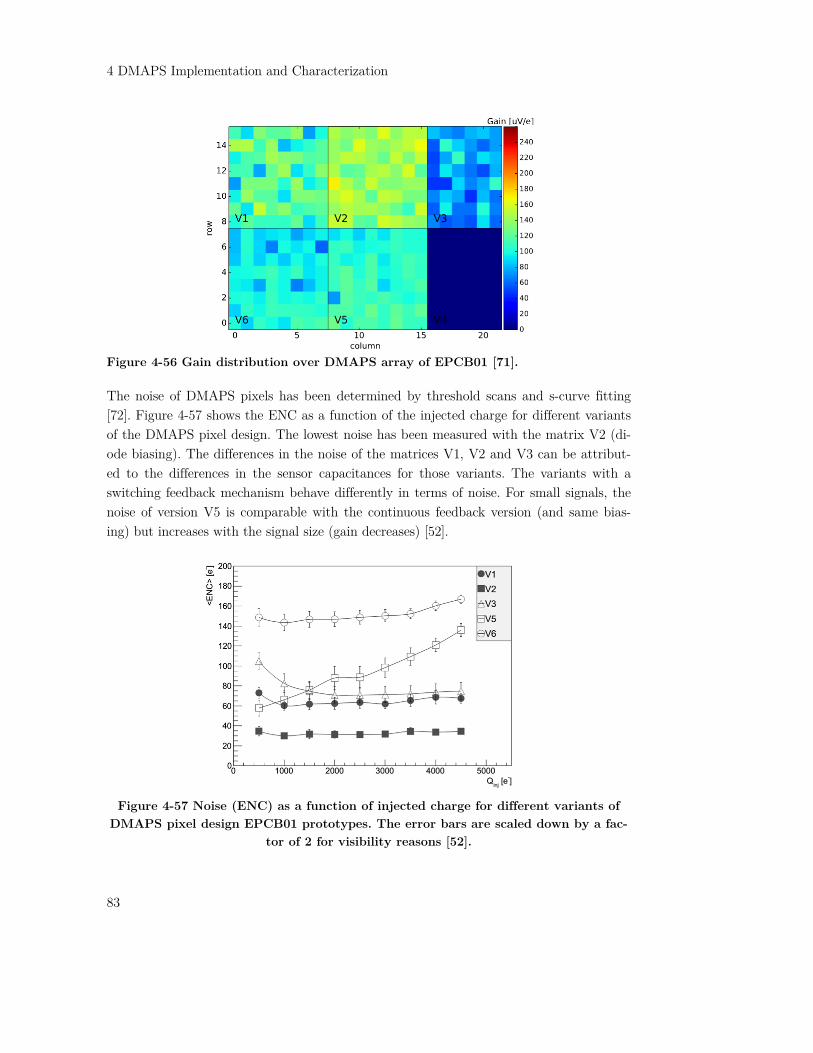
4 DMAPS Implementation and Characterization
83
Figure 4-56 Gain distribution over DMAPS array of EPCB01 [71].
The noise of DMAPS pixels has been determined by threshold scans and s-curve fitting [72]. Figure 4-57 shows the ENC as a function of the injected charge for different variants of the DMAPS pixel design. The lowest noise has been measured with the matrix V2 (di-ode biasing). The differences in the noise of the matrices V1, V2 and V3 can be attribut-ed to the differences in the sensor capacitances for those variants. The variants with a switching feedback mechanism behave differently in terms of noise. For small signals, the noise of version V5 is comparable with the continuous feedback version (and same bias-ing) but increases with the signal size (gain decreases) [52].
Figure 4-57 Noise (ENC) as a function of injected charge for different variants of
DMAPS pixel design EPCB01 prototypes. The error bars are scaled down by a fac-tor of 2 for visibility reasons [52].

Single pixel spectra are recorded with an ADC, directly connected at the analog output of the pixel amplifier. Figure 4-58 shows a single pixel spectrum for the baseline only and 55Fe source. One can distinguish the Mn Kα and Kβ lines of a 55Fe source. Using the Kα line for calibration the noise for this line is 31e- rms. This noise includes also signal fluc-tuations (Fano noise) and effect due to charge sharing to the neighbor pixel.
Figure 4-58 A single pixel spectrum of baseline and 55Fe source of EPCB01 (ver-
sion V2, room temperature).
A laser (680 nm, 4µm penetration depth in Si) with 3µm focused spot size entering from the backside of the sensor is used to characterize the charge collection homogeneity. The laser was moved in steps of 2µm. Figure 4-59 (a) shows the response of eight pixels scanned along one coordinate. The pixel responses of neighbors cross at half the value of the maximum signal when the laser is at the edge of two pixels. This suggests a good ho-mogeneity of the sensor. Figure 4-59 (b) shows the seed signal of two-dimensional scans. The inhomogeneity mainly comes from FE electronics gains and offset dispersion. To examine the effects of ionizing radiation (TID) on the electronics the chip has been irradiated with 60keV X-rays. The irradiations have been performed at room temperature up to a TID of 50Mrad in several steps. After each irradiation step, the chip has been an-nealed for 100 minutes at 80 C. A small array of different size transistors on the EPCB01 chip has been used to examine radiation effects of a single transistor device. Figure 4-60 shows the change in the transis-tor threshold and the transconductance (gm) as a function of the TID. One can observe that the threshold voltage for both transistor types shifts by less than 30 mV. The maxi-mum gm of the NMOS transistors degrades by less than 2% and for the PMOS by less than 15%. The radiation effects are more pronounced in the transistors with small channel widths.

4 DMAPS Implementation and Characterization
85
Figure 4-59 Response function of the laser scan along (left) column with 8 pixels
and (right) a 3x3 pixels 2D scan [53].
Figure 4-60 Change of (left) the transistor threshold and (right) gm as a function of
the ionizing dose for the OHC15L technology [52].
During the radiation the parameters of the amplifier have been characterized. Figure 4-61 shows the preamplifier response (version V2) for different radiation doses. One can ob-serve a change in the slope of the pulse when the pulse returns to the baseline (trailing edge). This change is most likely due to an increase of the leakage current in the feedback transistor which leads to a faster discharge of the amplifier. The change is not significant and can be corrected by changing the feedback current. Figure 4-62 shows the change in gain and noise as a function of the TID. The gain changes are in the order of 20% and the noise stays below 20e- for V2. No degradation of the digital part has been observed during irradiation. The OHC15L technology and the EPCB01 design show good tolerance against TID within the measured range of irradiation (below 50MRad).
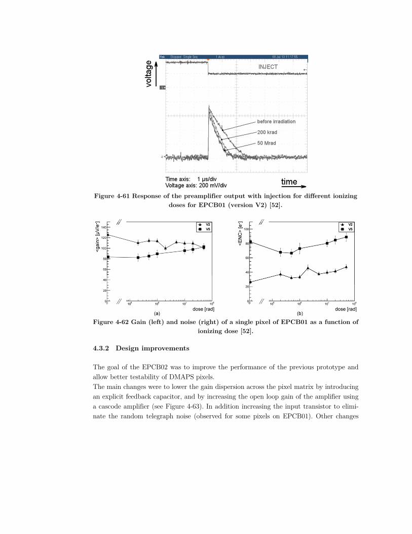
Figure 4-61 Response of the preamplifier output with injection for different ionizing
doses for EPCB01 (version V2) [52].
Figure 4-62 Gain (left) and noise (right) of a single pixel of EPCB01 as a function of
ionizing dose [52].
4.3.2 Design improvements
The goal of the EPCB02 was to improve the performance of the previous prototype and allow better testability of DMAPS pixels. The main changes were to lower the gain dispersion across the pixel matrix by introducing an explicit feedback capacitor, and by increasing the open loop gain of the amplifier using a cascode amplifier (see Figure 4-63). In addition increasing the input transistor to elimi-nate the random telegraph noise (observed for some pixels on EPCB01). Other changes
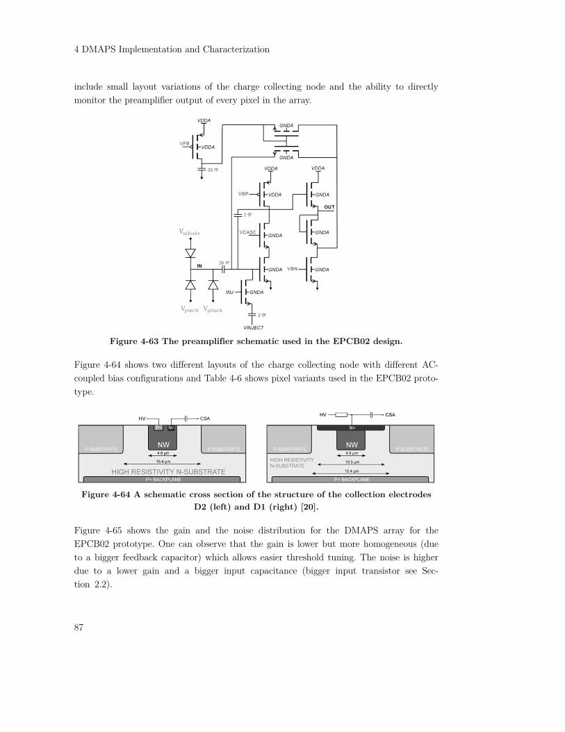
4 DMAPS Implementation and Characterization
87
include small layout variations of the charge collecting node and the ability to directly monitor the preamplifier output of every pixel in the array.
Figure 4-63 The preamplifier schematic used in the EPCB02 design.
Figure 4-64 shows two different layouts of the charge collecting node with different AC-coupled bias configurations and Table 4-6 shows pixel variants used in the EPCB02 proto-type.
Figure 4-64 A schematic cross section of the structure of the collection electrodes
D2 (left) and D1 (right) [20].
Figure 4-65 shows the gain and the noise distribution for the DMAPS array for the EPCB02 prototype. One can observe that the gain is lower but more homogeneous (due to a bigger feedback capacitor) which allows easier threshold tuning. The noise is higher due to a lower gain and a bigger input capacitance (bigger input transistor see Sec-tion 2.2).

Figure 4-65 Gain (top) and noise (bottom) distribution for the DMAPS array of the
EPCB02 prototype [71].
Table 4-6 Pixel variants used in the EPCB02 prototype.
Pixel variant
Collecting node
geometry
Biasing Couplingto sensor
FE Archi-tecture
Input transistor dimensions
Ar-ray size
V1 D2 diode AC continuous 1/0.3 µm 8x8V2 D2 resistor AC continuous 1/0.3 µm 8x8V3 D1 direct DC continuous 1/0.3 µm 8x6V4 D2 diode AC switched 1/0.3 µm 8x6V5 D1 diode AC switched 1/0.3 µm 8x8V6 D2 diode AC switched 2/0.150 µm 8x8
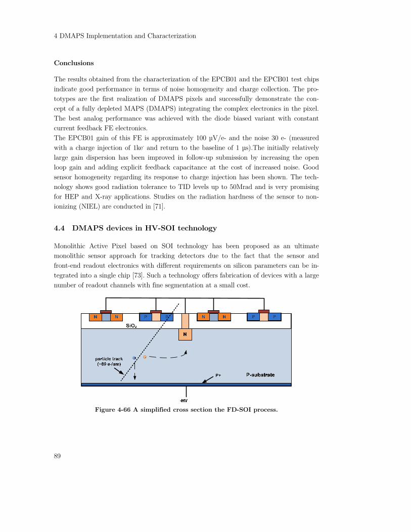
4 DMAPS Implementation and Characterization
89
Conclusions
The results obtained from the characterization of the EPCB01 and the EPCB01 test chips indicate good performance in terms of noise homogeneity and charge collection. The pro-totypes are the first realization of DMAPS pixels and successfully demonstrate the con-cept of a fully depleted MAPS (DMAPS) integrating the complex electronics in the pixel. The best analog performance was achieved with the diode biased variant with constant current feedback FE electronics. The EPCB01 gain of this FE is approximately 100 µV/e- and the noise 30 e- (measured with a charge injection of 1ke- and return to the baseline of 1 µs).The initially relatively large gain dispersion has been improved in follow-up submission by increasing the open loop gain and adding explicit feedback capacitance at the cost of increased noise. Good sensor homogeneity regarding its response to charge injection has been shown. The tech-nology shows good radiation tolerance to TID levels up to 50Mrad and is very promising for HEP and X-ray applications. Studies on the radiation hardness of the sensor to non-ionizing (NIEL) are conducted in [71].
4.4 DMAPS devices in HV-SOI technology
Monolithic Active Pixel based on SOI technology has been proposed as an ultimate monolithic sensor approach for tracking detectors due to the fact that the sensor and front-end readout electronics with different requirements on silicon parameters can be in-tegrated into a single chip [73]. Such a technology offers fabrication of devices with a large number of readout channels with fine segmentation at a small cost.
Figure 4-66 A simplified cross section the FD-SOI process.

The first prototypes of SOI-based MAPS were implemented with a FD-SOI (fully deplet-ed SOI) technology [74] [75], in which the whole body under the transistor gate is completely depleted. The primary application for FD-SOI process is high-speed and low power (standby) CMOS logic design. Unfortunately, the FD-SOI process by principle suffers significantly from TID effects [76], which manifest in transistor parameters change significantly due to charge build-up in the BOX layer (back gate effect). Several ways have been investigated to mitigate this problem, such as extra isolating implants in the handling wafer, or the use of double SOI wafers [77]. A new commercial HV-SOI process [78] that mitigates the back gate effect problems is being investigated. This process offers n- and p-well structures for active layers, which creates an additional isolation layer between the BOX and the active circuitry making transistor parameters insensitive to radiation effects in the BOX. This type of technology has been proposed in the past [79] but it is here for the first time realized in practice. The primary application for HV-SOI technology is high voltage (>200V) control devices.
Figure 4-67 Cross section of the thick-film HV-SOI process for p-type silicon sub-
strate and n-type collection diode.
A simplified cross-section of FD-SOI and thick-film SOI technologies is shown in Figure 4-66. In a SOI process, active devices are fabricated in a thin silicon layer on top of an insulating layer of silicon dioxide (buried oxide). The inactive layer underneath the BOX (handling wafer) can be used as a depleted sensor layer. The main difference of the thick-film SOI technology is that the active (transistor) layer is thick (few µm) compared to tens of nm in the case of FD-SOI. Multiple biased well structures give the possibility to isolate the transistor from any influence of charge build-up in the BOX. Both technologies allow access to the handling wafer to create a charge collecting diode and bias. A

4 DMAPS Implementation and Characterization
91
standard CMOS circuit can be realized in the active layer. The process provides the possibility to create high voltage (above 200V) transistors for power application. The expected depletion thickness of the handling wafer in this prototype is about 50µm.
Table 4-7 Overview of the technology options for the HV-SOI prototypes based on the X-FAB XT018 process.
Feature PropertyMOS channel length 180nm
Metals 6+1 layers, AluminumSupply rail 1.8 V (5V to 200V)
MOS transistor types low power/regularWafer type SOI, p-type handling(100Ωcm), p-type logic
4.4.1 XTB01 Prototype
To investigate the feasibility of the particle detector based on this X-FAB XT018 HV-SOI technology a prototype chip XTB01 has been designed with a simple diode structure and readout scheme. The technology options are summarized in Table 4-7. The device consists of 4 pixel arrays with three different pixel sizes (25, 50, 100 µm). For the time being, no back implant is being used and thus HV bias is applied laterally. The HV ring surrounds every pixel and a multi-guard ring structure is placed next to the chip edge. The layout of XTB01 chip is shown in Figure 4-68 and a cross section of the chip can be seen in Figure 4-69. An array of standalone P and N type transistors has been also implement at the periphery of the chip to measure the immunity against radiation effects.
Design
Since the handling wafer material is p-type, n-type implants are used as a collecting electrode. The readout transistors are placed adjacent to the collecting electrode. This region is separated from the diode by deep trench isolation (DTI). The implant structures for 25 and 50µm pixels are shown in Figure 4-70. P-type (p-stop) openings are placed be-tween pixels to "break" the electron accumulation layer underneath the BOX in particular after radiation. The majority of pixels use standard three transistor (3T) readout that allow direct access to the analog signal.

Figure 4-68 Layout of the XTB01 prototype [54].
This 3T readout scheme is widely used in various CMOS image sensors, and it makes it easy to compare sensor characteristics, such as the diode leakage current or noise performance, with other technologies. Figure 4-71 shows a block diagram of the 3T readout scheme. The reset transistor MRST is used to reset the pixel by dumping the integrated charge to the positive bias voltage. The transistor MSEL is activated to select the readout of the pixel, and MIN is the input transistor of a source follower. The current source is common to all the pixels in one column. A signal integrated on the input capacitance is directly proportional to the charge collected and scaled by input capacitance. The control signals are provided by two shift register arrays for row and column selection. One pixel is read one at a time in a rolling-shutter manner (see Chapter 2).
Figure 4-69 Cross-section through the XTB01 chip [54].
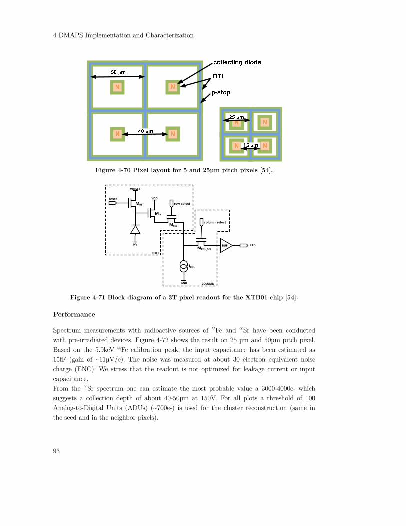
4 DMAPS Implementation and Characterization
93
Figure 4-70 Pixel layout for 5 and 25µm pitch pixels [54].
MRST
MSEL
MCOL_SEL
ICOL
BUF
reset
MIN
row select
column select
GND
VRESET
VDD
PAD
PIXEL
HV
COLUMN
Figure 4-71 Block diagram of a 3T pixel readout for the XTB01 chip [54].
Performance
Spectrum measurements with radioactive sources of 55Fe and 90Sr have been conducted with pre-irradiated devices. Figure 4-72 shows the result on 25 µm and 50µm pitch pixel. Based on the 5.9keV 55Fe calibration peak, the input capacitance has been estimated as 15fF (gain of ~11µV/e). The noise was measured at about 30 electron equivalent noise charge (ENC). We stress that the readout is not optimized for leakage current or input capacitance. From the 90Sr spectrum one can estimate the most probable value a 3000-4000e- which suggests a collection depth of about 40-50µm at 150V. For all plots a threshold of 100 Analog-to-Digital Units (ADUs) (~700e-) is used for the cluster reconstruction (same in the seed and in the neighbor pixels).

Table 4-8 Irradiation levels at different steps (TID dose from reactor background) for XTB01 prototype.
Fluence (neq/cm2) Dose(kRad)0 0
1 x 10¹³ 10 5 x 10¹³ 50 1 x 10¹³ 100 5 x 10¹³ 500
Figure 4-72 Single pixel spectra for 25µm pixel from 55Fe and 90Sr (single pixel and
3x3 clustered) radiative source at 150V bias and -20C [54].
The chips have been irradiated in the nuclear reactor at Ljubljana with 5 different doses of 1MeV neutrons. The chips were not pre-characterized. Measurements for different doses have been conducted with different devices. The neutron and TID doses are shown in Ta-ble 4-8. The performance of the HV-SOI pixel sensor has been studied with radioactive sources of 90Sr and 55Fe. Measured I-V characteristics for an entire chip for different neutron doses at room temperature are shown in Figure 4-73. With a bias voltage of 150V on 100 Ω-cm p-type substrate we expect about 50µm depletion thickness. One can observe a linear increase of the leakage current due to defects caused by neutron damage, while the breakdown volt-ages are increasing. Defects can act as recombination/generation centers and are responsi-ble for an increase of the leakage current.

4 DMAPS Implementation and Characterization
95
Figure 4-73 I–V characteristics for XTB01 for different neutron doses at 25C [54].
Figure 4-75 shows a 90Sr source spectrum after 1014 and 5x10¹⁴neq/cm2 for 50µm pixels. One can observe a clustered signal of about 4000e- at 250V after 1014neq/cm2. No signal is observed for 5x10¹⁴neq which may suggest inefficiencies between pixels caused by trapping. Losing charge due to trapping between pixels may be an effect of a large distance between collecting diodes and insufficient electrical field (see Figure 4-70). Figure 4-74 shows a 90Sr spectrum from clustered (3x3) 25µm pixels and the cluster distribution for 5x10¹⁴neq/cm2. Signals of about 4000e- are clearly seen, and this result would suggest that charge is not fully collected between pixels in the case of 50µm pixel pitch and 5x10¹⁴neq/cm2.
Figure 4-74 A 3x3 clustered pixel 90Sr and single cluster 55Fe and spectra for 25µm
pixel after 5x10¹⁴ neq/cm2 [54].
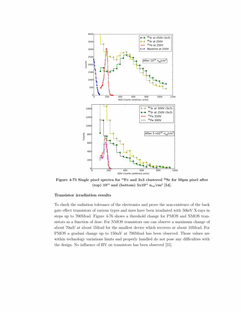
Figure 4-75 Single pixel spectra for 55Fe and 3x3 clustered 90Sr for 50µm pixel after
(top) 1014 and (bottom) 5x10¹⁴ neq/cm2 [54].
Transistor irradiation results
To check the radiation tolerance of the electronics and prove the non-existence of the back gate effect transistors of various types and sizes have been irradiated with 50keV X-rays in steps up to 700Mrad. Figure 4-76 shows a threshold change for PMOS and NMOS tran-sistors as a function of dose. For NMOS transistors one can observe a maximum change of about 70mV at about 5Mrad for the smallest device which recovers at about 10Mrad. For PMOS a gradual change up to 150mV at 700Mrad has been observed. Those values are within technology variations limits and properly handled do not pose any difficulties with the design. No influence of HV on transistors has been observed [55].

4 DMAPS Implementation and Characterization
97
Figure 4-76 Threshold change for various size (left) NMOS and (right) PMOS tran-
sistors as a function of the radiation does (TID) in the XT018 technology [55].
Figure 4-77 A Layout view of XT02 prototype.
4.4.2 XT02 Prototype
A second simple passive prototype chip XT02 has been designed for more detailed investigation on different guard ring structures and pixel diode geometries, especially focusing on the isolation between pixels and technological changes which should increase breakdown and reduce leakage current. Figure 4-77 shows the layout of the chip which consisting of different size pixel matrixes with different guard ring structures and simple transistor arrays. First measurements indicate lower leakage and higher breakdown voltage (see Figure 4-78).
Edge-TCT method (see Section 4.2.1) has been used to characterize charge collec-tion of the XT02 sensor for different fluence. Figure 4-79 shows the charge collection as a fraction of the distance/depth (y-axis) from the diode surface for different fluence. We
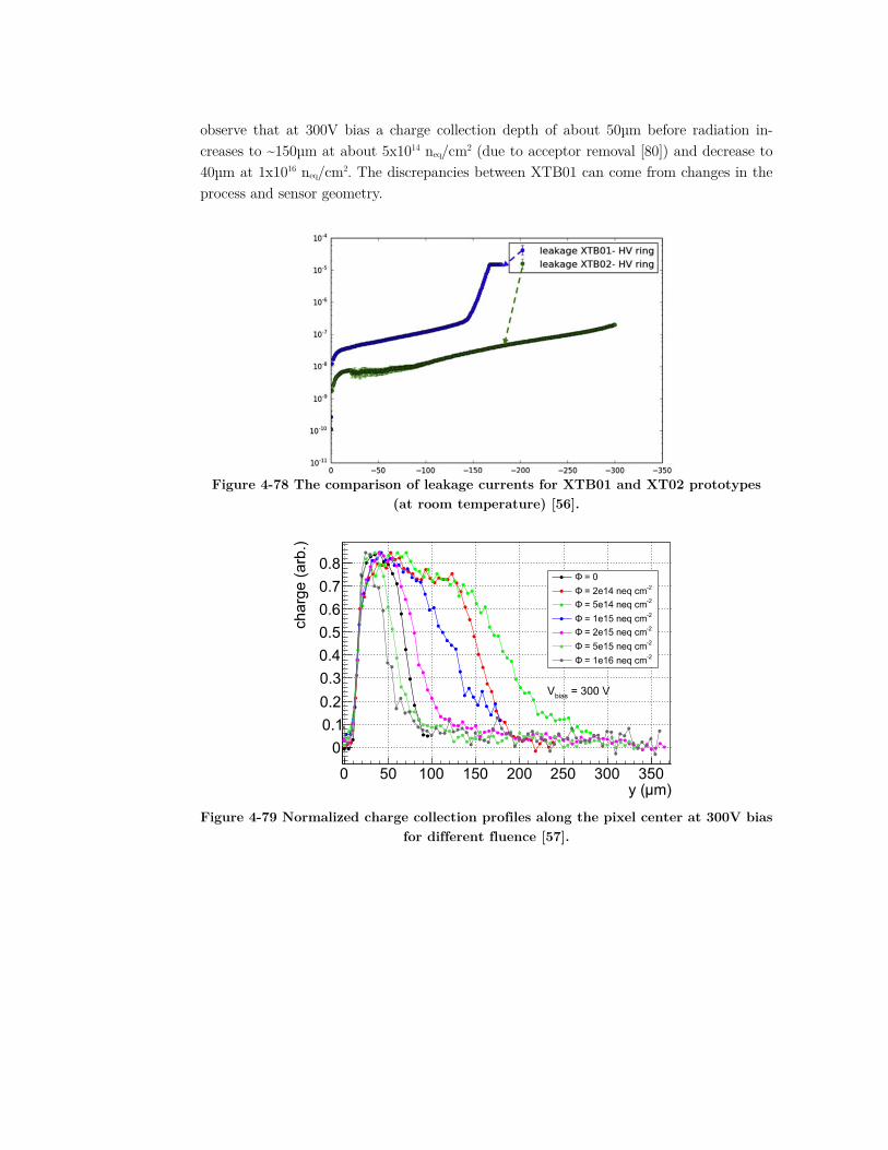
observe that at 300V bias a charge collection depth of about 50µm before radiation in-creases to ~150µm at about 5x10¹⁴ neq/cm2 (due to acceptor removal [80]) and decrease to 40µm at 1x10¹⁶ neq/cm2. The discrepancies between XTB01 can come from changes in the process and sensor geometry.
Figure 4-78 The comparison of leakage currents for XTB01 and XT02 prototypes
(at room temperature) [56].
Figure 4-79 Normalized charge collection profiles along the pixel center at 300V bias
for different fluence [57].

4 DMAPS Implementation and Characterization
99
Conclusions
An improved SOI-MAPS for ionizing radiation based on the HV-SOI technology has been developed. In comparison to existing FD-SOI devices, this technology makes use of thick epitaxial layer and multi-well structures to isolate the transistor channels from the BOX and make them immune to the back gate effects. Access to a handling wafer below the BOX allows using the substrate as a particle sensing device. The measurements with a 100Ωcm handling wafer indicate that more than 300V biased can be applied to the sensor. The signal from depleted part of above 100µm can still be collected after 1x10¹⁵neq/cm2. These first measurements indicate an encouraging prospect to use this technology for par-ticle detection and tracking in radiation harsh environments like LHC.

100
5 Conclusion
Future High Energy Physics experiments at the High Luminosity upgrade of the Large Hadron Collider (LHC) bring new challenges for pixel detectors. In particular, the in-crease in hit rates, radiation and the significant growth in detector area.
New directions in pixel technologies for HEP applications are Monolithic Active Pixel Sensors (MAPS). Depleted MAPS (DMAPS) sensors are fabricated in the high resistive silicon substrate which allowing charge collection of the entire signal generated in the depleted silicon bulk. As a consequence, fully monolithic high radiation tolerant devices can be achieved.
The primary asset offered by CMOS pixels is a low-cost potential which is especially attractive for large area coverage in the outer layers of the LHC experiments, were also radiation levels are less severe.
This thesis presents the development of new monolithic active pixel sensors. The pro-posed devices make use of commercially available CMOS technologies for the integration of a particle detector and readout electronics in one entity. The realization of the new monolithic active sensor requires a close relation with CMOS manufacturers and an un-derstanding of the semiconductor technology. Extensive process simulation allowed opti-mization of core sensor parameters. Various DMAPS prototypes in different technologies have been designed and manufactured for the first time. Prototypes allowed the character-ization of the basic components of active pixels sensors and the evaluation of device pa-rameters. Presented devices show strong indications that monolithic sensor can achieve very high radiation tolerance with parameters similar to the existing hybrid technology. Moreover, based on experience from this work improved passive sensor designs are being developed.
Presented work is one of the major factors for current high interests in DMAPS de-vices and is currently being followed by various groups.


102
Bibliography
[1] L. Rossi, P. Fischer, T. Rohe and N. Wermes, "Pixel Detectors From Fundamentals to Applications.", Springer, 2006.
[2] D. Greiffenberg, "The AGIPD detector for the European XFEL," JINST, vol. 7, p. C01103, 2012.
[3] M. Lindner., L. Blanquart, P. Fischer, H. Krüger and N. Wermes, "A Medical X-ray imaging chip with energy windowing," NIM A, vol. 465, pp. 229-234, 2001.
[4] S. R. Amendolia et al., "MEDIPIX: a VLSI chip for a GaAs pixel detector for digital radiology," NIM. A, vol. 422, pp. 201-205, 1999.
[5] B. Dierickx, G. Meynants and D. Scheffer, "Near 100% fill factor CMOS active pixels," Proceedings of the IEEE CCD & AIS Workshop, Brugge, Belgium, 1997.
[6] R. Turchetta et al., "A monolithic active pixel sensor for charged particle tracking and imaging using standard VLSI CMOS technology," NIM A, vol. 458, pp. 677-689, 2001.
[7] J. A. Ballin at al., "Monolithic Active Pixel Sensors (MAPS) in a Quadruple Well," Sensors, vol. 8, pp. 5336-5351, 2008.
[8] L. Greiner at al., "A MAPS based vertex detector for the STAR experiment at RHIC," NIMA, vol. A650, pp. 68-72, 2011.
[9] M. Šuljić, "ALPIDE: the Monolithic Active Pixel Sensor for the ALICE ITS upgrade," JINST, vol. 11, p. C11025, 2016.
[10] I. Peric, "A novel monolithic pixelated particle detector implemented in high-voltage CMOS technology," NIM A, vol. 852, p. 876–885, 2007.
[11] I. Peric, "Active pixel sensors in high-voltage CMOS technologies for ATLAS," JINST,

103
vol. 7, p. C08002, 2012.
[12] K. G. McKay, "Electron-hole Production in Germanium by Alpha Particles," Physical Review, vol. 84, p. 829, 1951.
[13] K.Iniewski, Semiconductor Radiation Detection Systems, K. Iniewski, Ed., CRC Press, 2010.
[14] D. E. Groom, V. Mokhov and S. Striganov, "Muon Stopping Power and Range Tables 10 MeV - 100 TeV," Atomic Data and Nuclear Data Tables, vol. 78, pp. 183-356, 2001.
[15] Particle Data Group, "Passage of particles through matter," Nuclear and Particle Physics, vol. 33, pp. 258-270, 2006.
[16] https://en.wikipedia.org/wiki/File:Pn_Junction_Diffusion_and_Drift.svg.
[17] B. V. Zeghbroeck, "Principles of Electronic Devices," http://ecee.colorado.edu/~bart/book/book/contents.htm, 2011.
[18] Wikipedia, "https://en.wikipedia.org/wiki/Active_pixel_sensor".
[19] F. de S. Campos, J. A. C. Ulson, J. E. C. Castanho and P. R. Aguiar, Noise Performance of Time-Domain CMOS Image Sensors, Photodiodes - From Fundamentals to Applications, InTech, 2012.
[20] M. Havránek, "Development of pixel front-end electronics using advanced deep submicron CMOS technologies," PhD Thesis, Bonn, 2014.
[21] M. Karagounis, "Analog Integrated CMOS Circuits for the Readout and Powering of Highly Segmented Detectors in Particle Physics Applications," PhD Thesis, Hagen, 2010.
[22] I. Peric, L. Blanquart, G. Comes, P. Denes and K. Einsweiler, P. Fischer, E. Mandelli, G. Meddele, "The FE-I3 readout chip for the ATLAS pixel detector," NIM A, vol. 565, 2006.
[23] M. Garcia-Sciveres et. al., "The FE-I4 pixel readout integrated circuit," NIM A, vol.

636, p. 155–159, April 2011.
[24] J. Lange, E. Cavallaro, S. Grinstein and I. L. Paz, "3D silicon pixel detectors for the ATLAS Forward Physics experiment," JINST, vol. 10, p. C03031, 2015.
[25] D. Schaefer et al., "The ATLAS Diamond Beam Monitor: Luminosity detector at the LHCN," NIM A, vol. 824, p. 459–461, July 2016.
[26] M. Karagounis et al., "Development of the ATLAS FE-I4 pixel readout IC for b-layer Upgrade and Super-LHC," TWEPP08, pp. 70-75, 2008.
[27] N. Parashar, "CMS Pixel Detector Upgrade," Proceedings of the DPF-2011 Conference, arXiv:1110.2125, 2011.
[28] RD53 Colaboration, "RD Collaboration Proposal:Development of pixel readout integrated circuits for extreme rate and radiation," CERN, Geneva, 2014.
[29] "http://home.cern/," [Online].
[30] S. Meroli, "Radiation damage for silicon detectors.," http://meroli.web.cern.ch/meroli/lecture_radiation_damage_silicon_detector.html, 2012.
[31] J. R. Schwank, "Radiation Effects in MOS Oxides," IEEE TNS, vol. 55, pp. 1833-1853, 2008.
[32] T. P. Ma and P. V. Dressendorfer, Ionizing Radiation Effects in MOS Devices and Circuits, John Wiley and Sons, 1989.
[33] E. H. Nicollian and J. R. Brews, MOS (Metal Oxide Semiconductor) Physics and Technology, John Wiley and Sons, 1982.
[34] T. R. Oldham and F. B. McLean, "Total Ionizing Dose Effects in MOS Oxides and Devices," IEEE TNS, vol. 50, pp. 483-499, 2003.
[35] A. Stabile, V. Liberali and C. Calligaro, "Design of a Rad-Hard Library of Digital Cells for Space Applications," Proc. Int. Conf. on Electronics, Circuits and Systems
105
(ICECS), pp. 149-152, 2008.
[36] I. Peric, "Design and Realisation of Integrated Circuits for the Readout of Pixel Sensors in High-Energy Physics and Biomedical Imaging," PhD Thesis, Bonn, 2004.
[37] F. Faccio and G. Cervelli, "Radiation-Induced Edge Effects in Deep Submicron CMOS Transistors," IEEE TNS, vol. 52, no. 6, pp. 2413 - 2420, 2005.
[38] G. Deptuch, "New Generation of Monolithic Active Pixel Sensors for Charged Particle Detection," PhD Thesis, Strasbourg, 2002.
[39] V. A. J. van Lint, T. M. Flanagan, R.E.Leadon, J. A. Naber and V.C.Rogers, Mechanisms of Radiation Effects in Electronic Materials, John Wiley & Sons, 1980.
[40] Gunnar Lindström, "Radiation damage in silicon detectors," NIM A, vol. 512, no. 1–2, pp. 30-43, 2003.
[41] M. Moll, "Radiation Damage in Silicon Particle Detectors", PhD Thesis, Hamburg, 1999.
[42] R. Wunstorf, "Systematische Untersuchungen zur Strahlenresistenz von SiliziumDetektoren fiir die Verwendung in Hochenergiephysik-Experimenten," PhD Thesis, Hamburg, 1992.
[43] M. Moll, "Radiation Damage to Semiconductor Devices," in Bethe Forum on Particle Detectors – Trends and Challenges, Bonn, https://indico.desy.de/event/BetheForumDetectors2014, 2014.
[44] D. Pennicard, G. Pellegrini, C. Fleta, R. Bates, V. O’Shea, C. Parkes and N. Tartoni, "Simulations of radiation-damaged 3D detectors for the Super-LHC," NIM A, vol. 592, pp. 16-25, 2008.
[45] G. Kramberger, V. Cindro, I. Mandic, M. Mikuz and M. Zavrtanik, "Effective trapping time of electrons and holes in different silicon materials irradiated with neutrons, protons and pions," NIM A, vol. 481, pp. 297-305, 2002.
[46] Synopsys, "Sentaurus TCAD," Synopsys, https://www.synopsys.com/, 2015.

[47] M. Benoit, A. Lounis and N. Dinu, "Simulation of charge multiplication and trap-assisted tunneling in irradiated planar pixel sensors," Nuclear Science Symposium Conference Record (NSS/MIC), 2010.
[48] D.-L. Pohl, T. Hemperek, I. Caicedo, L. Gonella, F. Hügging, J. Janssen, H. Krüger, A. Macchiolo, N. Owtscharenko and L. Vigani, "Radiation hard pixel sensors using high-resistive wafers in a 150 nm CMOS processing line," JINST, vol. 12, p. P06020, 2017.
[49] P. Rymaszewski, M. Barbero, P. Breugnon, S. Godiot, L. Gonella, T. Hemperek, T. Hirono, F. Hügging, H. Krüger and J. Liu, "Prototype Active Silicon Sensor in 150 nm HR-CMOS technology for ATLAS Inner Detector Upgrade," JINST, vol. 11, p. C02045, 2016.
[50] T. Hirono at al., "Characterization of Fully Depleted CMOS Active Pixel Sensors on High Resistivity Substrates for Use in a High Radiation Environment," in 2016 IEEE NSS-MIC Conference Record, 2016.
[51] T. Hirono et al., "CMOS pixel sensors on high resistive substrate for high-rate, high-radiation environments," NIM A, vol. 831, pp. 94-98, 2016.
[52] M. Havránek, T. Hemperek, H. Krüger, Y. Fu, L. Germic, T. Kishishita, C. Marinas, T. Obermann and N. Wermes, "DMAPS: a fully depleted monolithic active pixel sensor - analog performance characterization," JINST, vol. 10, p. P02013, 2015.
[53] T. Obermann, M. Havranek, T. Hempereka, F. Hügginga, T. Kishishita, H. Krüger, C. Marinasa and N. Wermesa, "Characterization of a Depleted Monolithic Active Pixel Sensor (DMAPS) prototype," JINST, vol. 10, p. C03049, 2015.
[54] T. Hemperek, T. Kishishita, H. Krüger and N. Wermes, "A Monolithic Active Pixel Sensor for ionizing radiation using a 180nm HV-SOI process," NIM A, vol. 796, pp. 8-12, 2015.
[55] S. Fernandez-Perez, M. Backhaus, H. Pernegger, T. Hemperek, T. Kishishita, H. Krueger and N. Wermes, "Radiation Hardness of a 180nm SOI Monolithic Active Pixel Sensor," NIM A, vol. 796, pp. 13-18, 2015.
[56] H. Pernegger, "Development of radiation hard CMOS active pixel sensors for HL-

107
LHC," NIM A, vol. 824, pp. 446-448, 2016.
[57] B. Hita, V. Cindro, A. Gorišek, T. Hemperek, T. Kishishita, G. Kramberger, H. Krüger, I. Mandić, M. Mikuž, N. Wermesc and M. Zavrtanik, "Charge collection properties in an irradiated pixel sensor built in HV-SOI process," arXiv:1701.06324, 2017.
[58] LFoundry, "http://www.europractice-ic.com/technologies_LFoundry.php".
[59] B. S. Avset and L. Evensen, "The effect of metal field plates on multiguard structures with floating p+ guard rings," NIM A, vol. 377, p. 397–403, 1996.
[60] Y. Okuto and C. R. Crowell, "Ionization coefficients in semiconductors: A nonlocalized property," Phys. Rev. B, vol. 10, pp. 4284-4296, 1974.
[61] O. Koybasi, G. Bolla and D. Bortoletto, "Guard Ring Simulations for n-on-p Silicon Particle Detectors," IEEE TNS, vol. 57, no. 5, pp. 2978 - 2986, 2010.
[62] I. Mandic, V. Cindro, A. Gorišek, B. Hiti, G. Kramberger, M. Mikuž, M. Zavrtanik, T. Hemperek, M. Daas and F. Hügging, "Neutron irradiation test of depleted CMOS pixel detector prototypes," JINST, vol. 12, p. P02021, 2017.
[63] I. Mandic, V. Cindro, A. Gorišek, G. Kramberger, M. Mikuž and M. Zavrtanik, "Edge-TCT measurements with the laser beam directed parallel to the strips," JINST, vol. 10, p. P08004, 2015.
[64] I. Mandić et al., "TCT measurements of HV-CMOS test structures irradiated with neutrons," in 11th "Trento" Workshop, https://indico.cern.ch/event/452766/, 2016.
[65] L. Gerhard, Semiconductor Radiation Detectors, Springer, 1999.
[66] I. Peric, "Hybrid Pixel Particle-Detector Without Bump Interconnection," IEEE TNS, vol. 56, no. 2, pp. 519 - 528, 2009.
[67] J. Liu at al., "HV/HR-CMOS sensors for the ATLAS upgrade concepts and test chip results," JINST, vol. 10, p. 3, 2015.
[68] W. Hillert, "The Bonn Electron Stretcher Accelerator ELSA: Past and future," Europ.
Phys. Jour. A, vol. 28, 2006.
[69] ESPROS Photonics AG homepage., "http://www.espros.ch.".
[70] M. Kachel and W. Duliński, "Fully depleted MAPS:Pegasus and MIMOSA 33," CPIX, Bonn, 2014.
[71] T.Obermann, "Characterization of a fully depleted monolithic pixel detector chip," PhD Thesis, Bonn, 2017.
[72] P. J. Bell and J. Grosse-Knetter, "Techniques for the measurement of common mode noise in binary read-out systems," NIM A, vol. 516, p. 153–159, january 2004.
[73] M. Amati et al., "Hybrid active pixel sensors and SOI inspired option," NIM A, vol. 511, pp. 265-270, 2003.
[74] A. Bulgheroni et al., "Monolithic active pixel detector realized in silicon on insulator technology," NIM A, vol. 535, pp. 398-403, 2004.
[75] Y. Arai et al., "First Results of 0.15μm CMOS SOI Pixel Detector," in NIC Symposium, Stanford, California, 2006.
[76] M. Kochiyama et al., "Radiation effects in silicon-on-insulator transistors with back-gate control method fabricated with OKI Semiconductor 0.20 um FD-SOI technology," NIM A, vol. 636, pp. S62 - S67, 2011.
[77] S. Honda et al., "Total ionization damage effects in double silicon-on-Insulator devices," in (NSS/MIC), 2013 IEEE, 2013.
[78] A. Hoelke et al., "A 200V partial SOI 0.18µm CMOS technology," Proc. of 22th International Symposium on Power Semiconductor Devices and IC’S (ISPSD), pp. 257-260, 2010.
[79] G. Deptuch, M. Trimp and Y. Raymod, "Monolithic Pixel Detectors in a Deep Submicron SoI Process," in TIPP, 2009.
[80] G. Kramberger et al., "Charge collection studies in irradiated HV-CMOS particle

109
detectors," JINST, vol. 11, p. P04007, 2016.

110
Acknowledgments
At this place, I want to thank Prof. Norbert Wermes for giving me freedom and support in the research work and being a role model as a sci-entist and as a person. I would especially like to thank for all the exceptional help in writing the thesis which was up to now the hardest part of my professional life.
I would especially like to thank Dr. Hans Krüger for support, comments, and discussions which led to the realization of the devices described in the thesis and much more.
Special thanks to late Dr. Wojciech Duliński who was my mentor for many years and without whom I would not be where I am now.
I would also like to thank Dr. Fabian Hügging for the discussions and advice and all my colleagues who work with me during design and meas-urements included in this thesis especially: Dr. Miroslav Havránek, Dr. Theresa Oberman, Dr. Tetsuichi Kishishita, Piotr Rymaszewski, Jens Jan-sen, David Pohl, Michael Daas and all others.
I would like to also thank Mr. Gerhard Spitzelsperger and Mr. Gerhard Viertlmeister from LFoundry, Dr. Martin Popp from ESPROS Photonics, Mr. Rainer Kaese from Toshiba, Dr. Konrad Bach and Dr. Alexander Hol-ke from XFab for they help in the realization of the projects.
Finally, I would like to thank my parents and siblings, and special my wife for quitting the job and coming with me to Bonn and continuous sup-port for over 10 years together.
