Embed Size (px)
Citation preview
IOP Publishing Journal Title
Journal XX (XXXX) XXXXXX https://doi.org/XXXX/XXXX
xxxx-xxxx/xx/xxxxxx 1 © xxxx IOP Publishing Ltd
Exploiting the Electrothermal Timescale in PrMnO3
RRAM for a compact, clock-less neuron exhibiting
biological spiking patterns
Omkar Phadke1, Jayatika Sakhuja1, Vivek Saraswat1, Udayan Ganguly1
1Department of Electrical Engineering, IIT Bombay, Mumbai, India. Email: [email protected]
Abstract
Spiking Neural Networks (SNNs) are gaining widespread momentum in the field of neuromorphic computing. These network
systems integrated with neurons and synapses provide computational efficiency by mimicking the human brain. It is desired to
incorporate the biological neuronal dynamics, including complex spiking patterns which represent diverse brain activities
within the neural networks. Earlier hardware realization of neurons was (1) area intensive because of large capacitors in the
circuit design, (2) neuronal spiking patterns were demonstrated with clocked neurons at the device level. To achieve more
realistic biological neuron spiking behavior, emerging memristive devices are considered promising alternatives. In this paper,
we propose, PrMnO3(PMO) -RRAM device-based neuron. The voltage-controlled electrothermal timescales of the compact
PMO RRAM device replace the electrical timescales of charging a large capacitor. The electrothermal timescale is used to
implement an integration block with multiple voltage-controlled timescales coupled with a refractory block to generate
biological neuronal dynamics. Here, first, a Verilog-A implementation of the thermal device model is demonstrated, which
captures the current-temperature dynamics of the PMO device. Second, a driving circuitry is designed to mimic different spiking
patterns of cortical neurons, including Intrinsic bursting (IB) and Chattering (CH). Third, a neuron circuit model is simulated,
which includes the PMO RRAM device model and the driving circuitry to demonstrate the asynchronous neuron behavior.
Finally, a hardware-software hybrid analysis is done in which the PMO RRAM device is experimentally characterized to mimic
neuron spiking dynamics. The work presents a realizable and more biologically comparable hardware-efficient solution for
large-scale SNNs.
Keywords: PrMnO3 (PMO), RRAM, Neuron Spiking Patterns, Spiking Neural Network (SNN)
1. Introduction
A Spiking Neural Network (SNN) mimics the human brain
to perform complex computations. The ability to perform
tasks parallelly, along with low power consumption, gives
SNN an edge over traditional von Neumann architecture,
which is limited by the von Neumann bottleneck. The human
brain consists of two main components; a neuron, which fires
according to the input signal, and a synapse, which
interconnects two neurons. Whenever a neuron receives a
stimulus, it integrates the input signal to its membrane
potential. Once the membrane potential reaches a threshold, it
falls back down to low levels, exhibiting a spike. The spike
timing of the neuron and the strength of the synapse are crucial
for information processing. As illustrated in Fig.1, a neuron
can exhibit different spiking patterns, and each spiking pattern
plays a unique role in the functioning of the brain [1]. For
example, neurons that exhibit 'Tonic Bursting' are thought to
be responsible for the 'Gamma Wave Oscillations' in the brain.
Some neurons are also used for concentration gradient
computations in chemotaxis in C. elegans, which is used to
translate from biology to algorithms [2]. Since the biological
neurons exhibit a rich variety of spiking patterns, we need
artificial neurons which mimic these spiking patterns to build
SNNs which can perform a wider variety of tasks (Fig.1).
Further, the refractory period occurs after spiking when the
neuron is quiescent and does not effectively integrate inputs.
The tuning of the refractory period is another critical element
of the neuron to control the dynamics of brain waves [3] and
navigational circuits [4]. Thus, the neuron has various
timescales – both during spiking and refractory phases.
Previously, many mathematical models of the neuron have
demonstrated different spiking patterns of the cortical neuron.
A popular model has been the Izhikevich Model, which is
biologically plausible and computationally efficient [5]. While
such models help study large-scale SNNs in a simulation
environment and providing us insights into brain functioning,
they are not useful for hardware implementation of SNNs. For
Journal XX (XXXX) XXXXXX Author et al
2
hardware realization of SNNs, we need devices that mimic
different spiking patterns of the neuron while being area
efficient and consuming less power.
Various device-based neurons have been demonstrated [6]-
[11]. Here, the 'integration' operation is implemented by
charging the external capacitor. The size of the capacitor and
the input determine the spiking frequency, and to show
different integration timescales, the area of the capacitor needs
to be changed. Also, these neurons consume a large area,
making the large-scale implementation of SNNs challenging
especially when realizing longer real-world signal timescales
(e.g., speech). Different spiking patterns have also been
implemented using digital circuitry [12]. The implementation
can demonstrate a wide range of spiking patterns while being
biologically plausible. However, the circuitry of a single
neuron is complex as it involves multiple buffers, counters,
multiplexers, and pipelines (which consist of adders), and the
implementation is clocked. It shows an implementation for a
small SNN, but for bigger SNNs, the resulting digital circuitry
will be large and complex.
Recently, Resistive Random-Access Memory (RRAM)
based implementation of neurons was demonstrated, which
utilized the internal timescales of the RRAM device (either
gradual resistive switching or electrothermal timescale) to
perform the integration operation, which eliminated the need
of using an external capacitor [13]-[14]. Specifically, a Pr1-
xCaxMnO3 (PCMO) based RRAM device was proposed to
implement an Integrate and Fire (IF) neuron [13]. The paper
also demonstrated different spiking patterns, such as
Intrinsically Bursting (IB), and Chattering (CH) patterns.
Also, the neuron utilized the internal timescale of resistive
switching to perform integration operation. The PCMO
RRAM can show different conductance levels and exhibits
different spiking frequencies for these different conductance
levels. These two features eliminated the need for an external
capacitor. The major disadvantages of the PCMO RRAM
neuron implementation were that the neuron did not exhibit a
'Leaky' behavior, which is integral to the functioning of a
biological neuron, and it utilizes a clock to operate, whereas
human brains do not use a clock [15].
A PrMnO3 (PMO) RRAM-based Leaky IF (LIF) neuron
was demonstrated experimentally [14]. PMO-based RRAM
devices are non-filamentary and highly scalable, making them
attractive for compact neurons. Here, the internal
electrothermal timescales in PMO material were used to
perform integration, eliminating the use of an external
capacitor. The PMO RRAM-based neuron was asynchronous
and demonstrated only a single spiking pattern.
In this paper, we demonstrate an asynchronous, capacitor-
free, PMO RRAM-based neuron that can exhibit different
spiking patterns of a cortical neuron. The neuron utilizes the
multiple voltage-controlled electrothermal timescales of PMO
RRAM to construct an integration block coupled to a
refractory block to enable a compact capacitor-free timescale
control. We propose a simulation setup consisting of a
physics-based Verilog-A model of the RRAM, and a
behaviorally modeled driving circuit, to model and predict
different spiking patterns. The voltage across the device from
the simulation setup is extracted, approximated, and applied
across the PMO RRAM to experimentally demonstrate the
different biological spiking patterns. The work provides a
strategy to investigate different biological spiking patterns in
simulations as well as experimentally in area-efficient
memristor-based synaptic arrays.
2. Device Details
The stack of PMO-based RRAM is as shown in Fig.2a. The
Silicon (Si) substrate is used for RRAM fabrication. SiO2 is
thermally grown on the Si wafer followed by deposition
of a bilayer of Titanium (Ti) followed by Platinum (Pt)
deposited through DC sputtering. A blanket layer of PMO
film (60 nm) is then deposited using RF sputtering at room
temperature. The PMO film is annealed in O2 ambient
at 750°C for 30 seconds. Finally, the top metal, tungsten (W),
contact pads are patterned through UV lithography and metal
lift-off process.
Figure 1 Motivation figure. Implementation of diverse
neuronal spiking patterns observed in human brain.
through RRAM devices will be computationally efficient
for neural networks.
Figure 2 (a) Device Schematic of fabricated PMO based
RRAM (b) The volatile DC-IV characteristics of PMO
RRAM device with C2C variation. The dotted blue lines
show data for different cycles. The solid blue line is the
mean value. The inset shows the enlarged version of the
volatile hysteresis loop.
(a) (b)
Journal XX (XXXX) XXXXXX Author et al
3
The resulting device structure is a metal-insulator-metal
(MIM) structure, with reactive metal W and noble metal Pt as
the top and bottom electrodes, as shown in Fig. 2a. If a
negative bias is applied to the reactive electrode, the device
goes to a Low Resistance State (LRS). If a positive bias is
applied to the reactive electrode, the device goes to a High
Resistance State (HRS). The non-volatile resistance change
occurs due to modulation of trap density at the reactive
electrode interface. The current through the device follows the
Space Charge Limited Current (SCLC) mechanism [16]-[17].
When the device is in LRS state, and a negative voltage sweep
is applied, the device exhibits a volatile-resistance change.
The DC IV characteristics of volatile switching are as shown
in Fig. 2b. For the experiments demonstrated in the paper, the
device is in LRS. The volatile switching shown by the device
occurs due to the electrothermal mechanism. As voltage is
applied, a current start to flow through the device. At higher
currents the device temperature increases, owing to Joule
heating, which in turn increases the current through the device.
The generated heat is trapped inside the device due to the low
thermal conductivity of the PMO material (1.48Wcm-1K-
1)[18]. At a certain threshold voltage, the interplay between
the current and temperature results in positive feedback, which
leads to a sharp shoot-up in current.
3. Electrothermal RRAM Device Model
To capture the device's current-temperature dynamics, an
electrothermal model is demonstrated. The current is
calculated using the analytical model shown in equations (1-
3), and the temperature is calculated using equation (4) [16].
I = IOhmic + ISCLC (1)
IOhmic = qAμNv (T
Tamb
)3 2⁄
e(−
qϕBkT
)(
V
L) (2)
ISCLC = AμϵoϵPMO (Nv
NT
) (T
Tamb
)3 2⁄
e(−
qEtrap
kT)
(V2
L3) (3)
T − Tamb
Rth
+ Cth
dT
dt = IV (4)
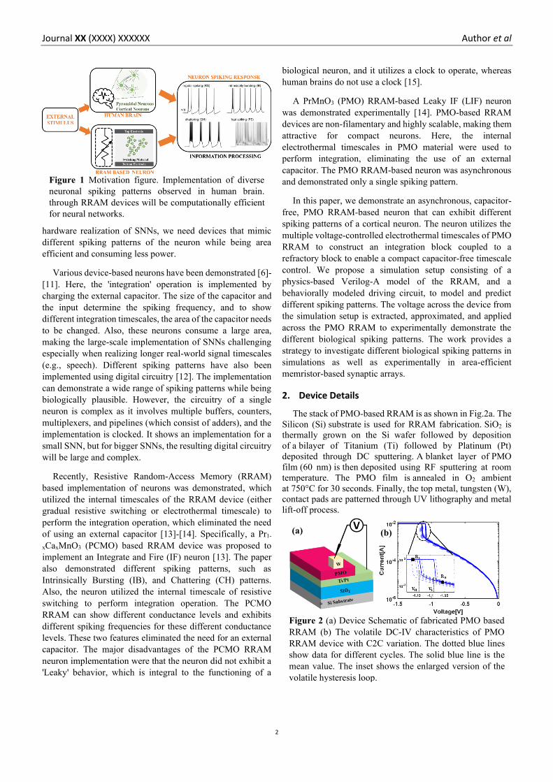
The equations are modeled in Verilog-A and simulated in
Cadence Virtuoso. The flowchart for the model is as shown in
Fig. 3. The model is initialized by setting the temperature as
ambient temperature (300K) and applying voltage bias. Using
equations (1) to (4), temperature and current are solved self-
consistently.
The equivalent thermal coefficients are 𝑅𝑡ℎ (thermal
resistance) and 𝐶𝑡ℎ (thermal capacitance). Here, the
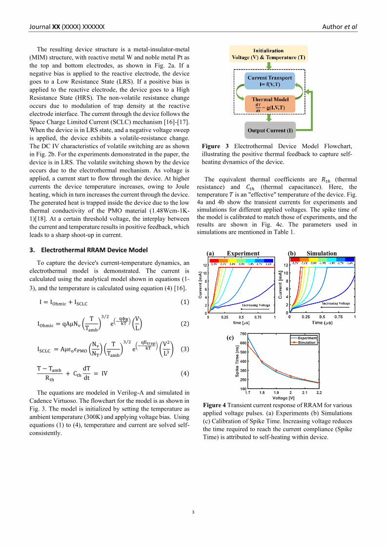
temperature 𝑇 is an "effective" temperature of the device. Fig.
4a and 4b show the transient currents for experiments and
simulations for different applied voltages. The spike time of
the model is calibrated to match those of experiments, and the
results are shown in Fig. 4c. The parameters used in
simulations are mentioned in Table 1.
Figure 3 Electrothermal Device Model Flowchart,
illustrating the positive thermal feedback to capture self-
heating dynamics of the device.
(a) (b)
(c)
Figure 4 Transient current response of RRAM for various
applied voltage pulses. (a) Experiments (b) Simulations
(c) Calibration of Spike Time. Increasing voltage reduces
the time required to reach the current compliance (Spike
Time) is attributed to self-heating within device.
Experiment Simulation
Journal XX (XXXX) XXXXXX Author et al
4
Model Symbol Quantity Value
Analytical
Model
μ Mobility 17.5 cm2/Vs
ϕB Barrier Height 0.3151 eV
ϵPMO Dielectric
Constant 30
Nv Density of
States 8.16×1019 cm-3
Etrap Trap Level 0.06 eV
NT Trap Density 3.15×1021 cm-3
Device
L Length 65 nm
A Area 10×10 𝜇m2
Thermal
Model
Tamb Ambient
Temperature 300 K
Rth Thermal
Resistance 3×10⁴ K/W
Cth Thermal
Capacitance 3.25 pJ/K
Table 1: Parameters Used in the Model
4. Input Voltage Dependent Electrothermal Timescale Control
As shown in the flowchart Fig. 3, current and temperature
are dependent quantities. Therefore, with an increase in
current, temperature increases, which further increases the
current. The positive feedback between current and
temperature results in a current shoot-up. A constant voltage
pulse of different magnitudes is applied across the device, and
the current through the device is observed (Fig. 4). The time
for the current to shoot up and reach the compliance depends
upon the applied voltage. Thus, a higher voltage will trigger
a faster shoot-up, and a lower voltage will slow down the
current shoot-up. The current-temperature time dynamic is
used as an integration timescale in the proposed PMO RRAM-
based neuron.
5. Circuit Implementation:
5.1 Exhibiting Different Spiking Patterns
Biological neurons are capable of exhibiting different
spiking patterns. To mimic that behavior in hardware using
RRAM, the following circuit concept and operation are
proposed. A neuron integrates the input with a timescale to
raise its membrane potential, and a spike is issued when a
threshold is reached. The spike patterns are characterized by
the positioning of spikes or spike timings for constant input.
A neuron based on RRAM can generate spike patterns by
using the electrothermal timescale for integration controlled
by the input voltage, which is slowly time-varying input from
synapses. Complex biological spiking patterns can be
generated by modulating the input voltage applied either
directly or with an additional resistive drop across RRAM
based on an internal binary state variable of the neuron to
modulate the integration timescales dynamically. Further, the
refractory period control is enabled by coupling another
RRAM block to the integration block – whose electrothermal
timescale is voltage-controlled.
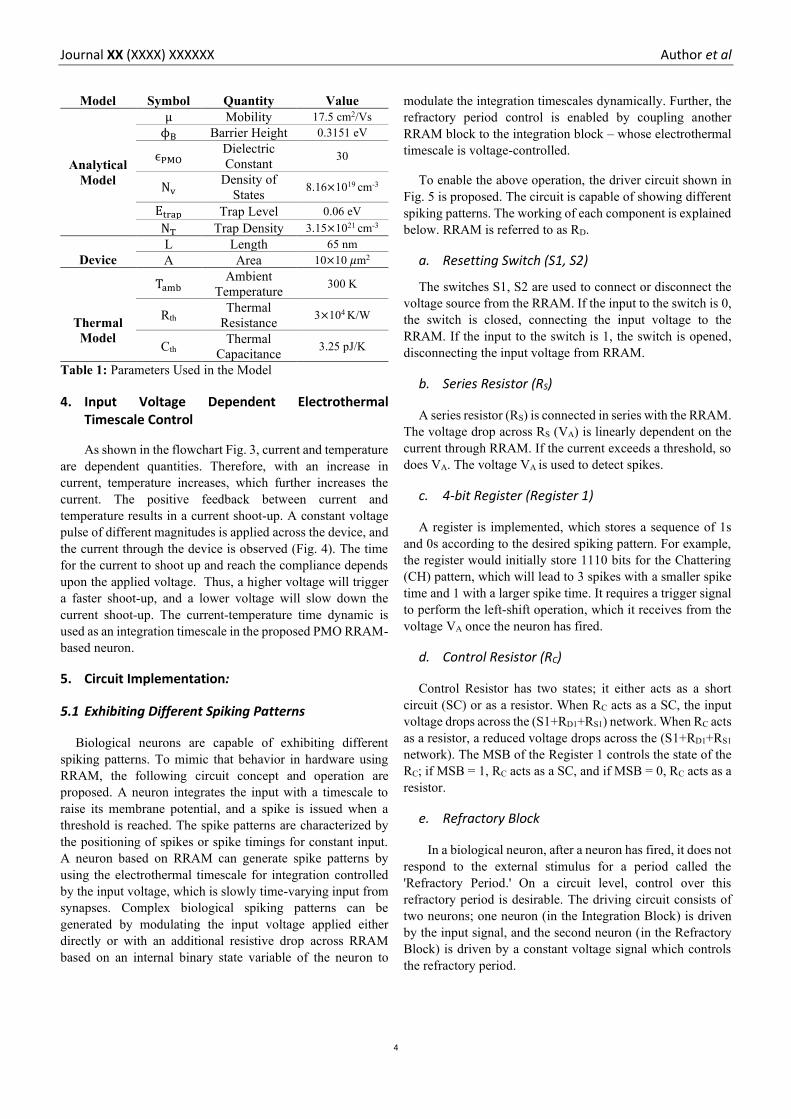
To enable the above operation, the driver circuit shown in
Fig. 5 is proposed. The circuit is capable of showing different
spiking patterns. The working of each component is explained
below. RRAM is referred to as RD.
a. Resetting Switch (S1, S2)
The switches S1, S2 are used to connect or disconnect the
voltage source from the RRAM. If the input to the switch is 0,
the switch is closed, connecting the input voltage to the
RRAM. If the input to the switch is 1, the switch is opened,
disconnecting the input voltage from RRAM.
b. Series Resistor (RS)
A series resistor (RS) is connected in series with the RRAM.
The voltage drop across RS (VA) is linearly dependent on the
current through RRAM. If the current exceeds a threshold, so
does VA. The voltage VA is used to detect spikes.
c. 4-bit Register (Register 1)
A register is implemented, which stores a sequence of 1s
and 0s according to the desired spiking pattern. For example,
the register would initially store 1110 bits for the Chattering
(CH) pattern, which will lead to 3 spikes with a smaller spike
time and 1 with a larger spike time. It requires a trigger signal
to perform the left-shift operation, which it receives from the
voltage VA once the neuron has fired.
d. Control Resistor (RC)
Control Resistor has two states; it either acts as a short
circuit (SC) or as a resistor. When RC acts as a SC, the input
voltage drops across the (S1+RD1+RS1) network. When RC acts
as a resistor, a reduced voltage drops across the (S1+RD1+RS1
network). The MSB of the Register 1 controls the state of the
RC; if MSB = 1, RC acts as a SC, and if MSB = 0, RC acts as a
resistor.
e. Refractory Block
In a biological neuron, after a neuron has fired, it does not
respond to the external stimulus for a period called the
'Refractory Period.' On a circuit level, control over this
refractory period is desirable. The driving circuit consists of
two neurons; one neuron (in the Integration Block) is driven
by the input signal, and the second neuron (in the Refractory
Block) is driven by a constant voltage signal which controls
the refractory period.
f. Toggle Block
The toggle block ensures that either the Integration Block
or the Refractory block stays active at a given time. The toggle
block has an OR gate, which detects if either of the neurons
has spiked via voltage VA, and a 2-bit register (Register 2)
whose MSB controls the switches S1 and S2. Once a neuron
has fired, the 2-bit register performs a left shift operation and
flips the MSB bit (as only 0 and 1 is stored, and MSB is
connected back to LSB). This disconnects the neuron which
has fired from the voltage source and reconnects the other
neuron to its voltage supply. This operation of switching
between 2 blocks is repeated as long as the neuron spikes.
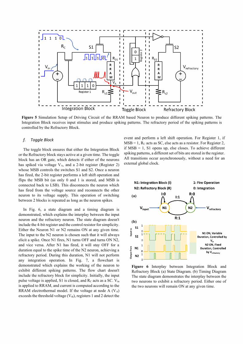
In Fig. 6, a state diagram and a timing diagram is
demonstrated, which explains the interplay between the input
neuron and the refractory neuron. The state diagram doesn't
include the 4-bit register and the control resistor for simplicity.
Either the Neuron N1 or N2 remains ON at any given time.
The input to the N2 neuron is chosen such that it will always
elicit a spike. Once N1 fires, N1 turns OFF and turns ON N2,
and vice versa. After N1 has fired, it will stay OFF for a
duration equal to the spike time of the N2 neuron, achieving a
refractory period. During this duration, N1 will not perform
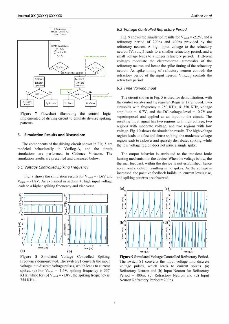
any integration operation. In Fig. 7, a flowchart is
demonstrated which explains the working of the neuron to
exhibit different spiking patterns. The flow chart doesn't
include the refractory block for simplicity. Initially, the input
pulse voltage is applied, S1 is closed, and RC acts as a SC. Vin
is applied to RRAM, and current is computed according to the
RRAM electrothermal model. If the voltage at node A (VA)
exceeds the threshold voltage (Vth), registers 1 and 2 detect the
event and perform a left shift operation. For Register 1, if
MSB = 1, RC acts as SC, else acts as a resistor. For Register 2,
if MSB = 1, S1 opens up, else closes. To achieve different
spiking patterns, a different set of bits are stored in the register.
All transitions occur asynchronously, without a need for an
external global clock.
Figure 5 Simulation Setup of Driving Circuit of the RRAM based Neuron to produce different spiking patterns. The
Integration Block receives input stimulus and produce spiking patterns. The refractory period of the spiking patterns is
controlled by the Refractory Block.
Figure 6 Interplay between Integration Block and
Refractory Block (a) State Diagram. (b) Timing Diagram
The state diagram demonstrates the interplay between the
two neurons to exhibit a refractory period. Either one of
the two neurons will remain ON at any given time.
(b)
(a)
Journal XX (XXXX) XXXXXX Author et al
6
6. Simulation Results and Discussion:
The components of the driving circuit shown in Fig. 5 are
modeled behaviorally in Verilog-A, and the circuit
simulations are performed in Cadence Virtuoso. The
simulation results are presented and discussed below.
6.1 Voltage Controlled Spiking Frequency
Fig. 8 shows the simulation results for Vinput = -1.6V and
Vinput = -1.8V. As explained in section 4, high input voltage
leads to a higher spiking frequency and vice versa.
6.2 Voltage Controlled Refractory Period
Fig. 9 shows the simulation results for Vinput = -2.2V, and a
refractory period of 200ns and 400ns provided by the
refractory neuron. A high input voltage to the refractory
neuron (Vrefractory) leads to a smaller refractory period, and a
small voltage leads to a longer refractory period. Different
voltages modulate the electrothermal timescales of the
refractory neuron and hence the spike timing of the refractory
neuron. As spike timing of refractory neuron controls the
refractory period of the input neuron, Vrefractory controls the
refractory period.
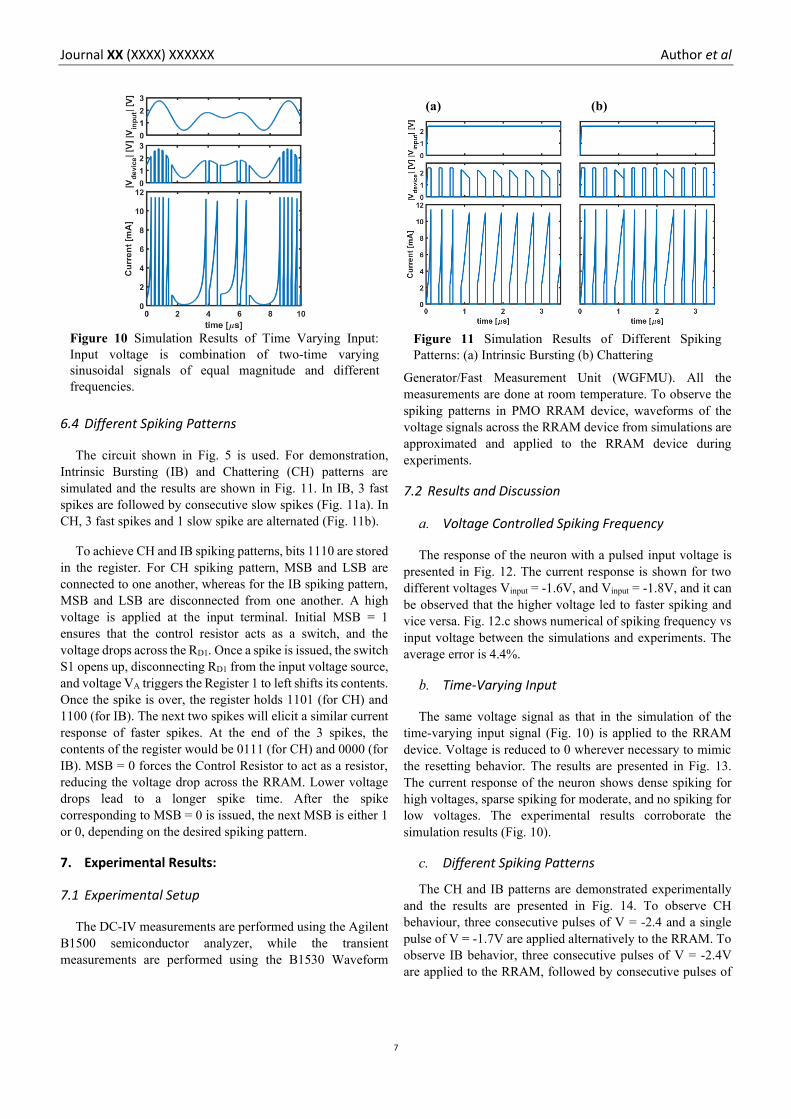
6.3 Time Varying Input
The circuit shown in Fig. 5 is used for demonstration, with
the control resistor and the register (Register 1) removed. Two
sinusoids with frequency = 250 KHz, & 350 KHz, voltage
amplitude = -0.7V, and the DC voltage level = -0.7V are
superimposed and applied as an input to the circuit. The resulting input signal has two regions with high voltage, two
regions with moderate voltage, and two regions with low
voltage. Fig. 10 shows the simulation results. The high voltage
region leads to a fast and dense spiking, the moderate voltage
region leads to a slower and sparsely distributed spiking, while
the low voltage region does not issue a single spike.
The output behavior is attributed to the transient Joule
heating mechanism in the device. When the voltage is low, the
thermal feedback within the device is not established, hence
no current shoot-up, resulting in no spikes. As the voltage is
increased, the positive feedback builds up, current levels rise,
and spiking patterns are observed.
Figure 7 Flowchart illustrating the control logic
implemented of driving circuit to emulate diverse spiking
patterns.
Figure 8 Simulated Voltage Controlled Spiking
Frequency demonstrated. The switch S1 converts the input
voltage into discrete voltage pulses, which leads to current
spikes. (a) For Vinput = -1.6V, spiking frequency is 537
KHz, while for (b) Vinput = -1.8V, the spiking frequency is
754 KHz.
(a) (b)
(a)
(b) (d)
(c)
Figure 9 Simulated Voltage Controlled Refractory Period.
The switch S1 converts the input voltage into discrete
voltage pulses, which leads to current spikes. (a)
Refractory Neuron and (b) Input Neuron for Refractory
Period = 400ns, (c) Refractory Neuron and (d) Input
Neuron Refractory Period = 200ns.
Journal XX (XXXX) XXXXXX Author et al
7
6.4 Different Spiking Patterns
The circuit shown in Fig. 5 is used. For demonstration,
Intrinsic Bursting (IB) and Chattering (CH) patterns are
simulated and the results are shown in Fig. 11. In IB, 3 fast
spikes are followed by consecutive slow spikes (Fig. 11a). In
CH, 3 fast spikes and 1 slow spike are alternated (Fig. 11b).
To achieve CH and IB spiking patterns, bits 1110 are stored
in the register. For CH spiking pattern, MSB and LSB are
connected to one another, whereas for the IB spiking pattern,
MSB and LSB are disconnected from one another. A high
voltage is applied at the input terminal. Initial MSB = 1
ensures that the control resistor acts as a switch, and the
voltage drops across the RD1. Once a spike is issued, the switch
S1 opens up, disconnecting RD1 from the input voltage source,
and voltage VA triggers the Register 1 to left shifts its contents.
Once the spike is over, the register holds 1101 (for CH) and
1100 (for IB). The next two spikes will elicit a similar current
response of faster spikes. At the end of the 3 spikes, the
contents of the register would be 0111 (for CH) and 0000 (for
IB). MSB = 0 forces the Control Resistor to act as a resistor,
reducing the voltage drop across the RRAM. Lower voltage
drops lead to a longer spike time. After the spike
corresponding to MSB = 0 is issued, the next MSB is either 1
or 0, depending on the desired spiking pattern.
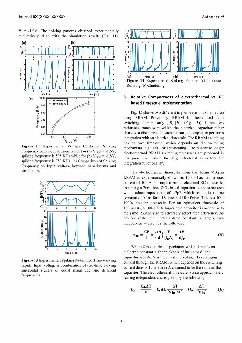
7. Experimental Results:
7.1 Experimental Setup
The DC-IV measurements are performed using the Agilent
B1500 semiconductor analyzer, while the transient
measurements are performed using the B1530 Waveform
Generator/Fast Measurement Unit (WGFMU). All the
measurements are done at room temperature. To observe the spiking patterns in PMO RRAM device, waveforms of the
voltage signals across the RRAM device from simulations are
approximated and applied to the RRAM device during
experiments.
7.2 Results and Discussion
a. Voltage Controlled Spiking Frequency
The response of the neuron with a pulsed input voltage is
presented in Fig. 12. The current response is shown for two
different voltages Vinput = -1.6V, and Vinput = -1.8V, and it can
be observed that the higher voltage led to faster spiking and
vice versa. Fig. 12.c shows numerical of spiking frequency vs
input voltage between the simulations and experiments. The
average error is 4.4%.
b. Time-Varying Input
The same voltage signal as that in the simulation of the
time-varying input signal (Fig. 10) is applied to the RRAM
device. Voltage is reduced to 0 wherever necessary to mimic
the resetting behavior. The results are presented in Fig. 13.
The current response of the neuron shows dense spiking for
high voltages, sparse spiking for moderate, and no spiking for
low voltages. The experimental results corroborate the
simulation results (Fig. 10).
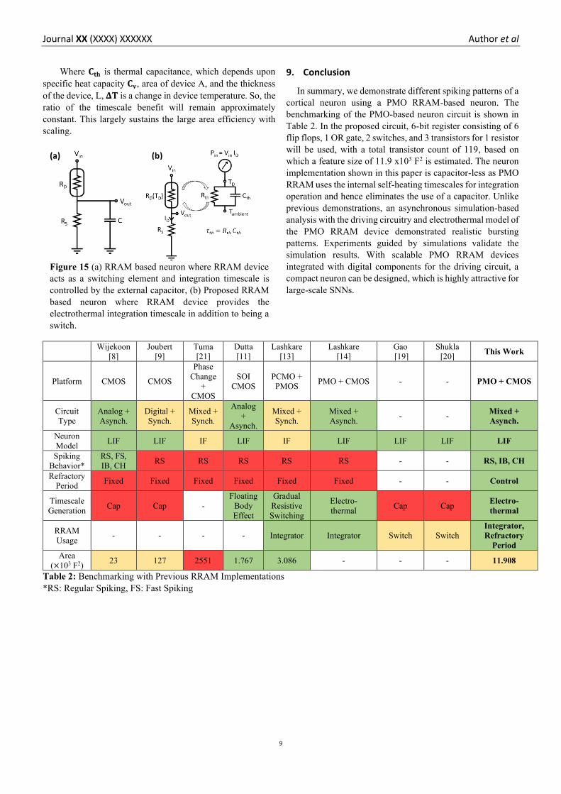
c. Different Spiking Patterns
The CH and IB patterns are demonstrated experimentally
and the results are presented in Fig. 14. To observe CH
behaviour, three consecutive pulses of V = -2.4 and a single
pulse of V = -1.7V are applied alternatively to the RRAM. To
observe IB behavior, three consecutive pulses of V = -2.4V
are applied to the RRAM, followed by consecutive pulses of
Figure 10 Simulation Results of Time Varying Input:
Input voltage is combination of two-time varying
sinusoidal signals of equal magnitude and different
frequencies.
Figure 11 Simulation Results of Different Spiking
Patterns: (a) Intrinsic Bursting (b) Chattering
(a) (b)
Journal XX (XXXX) XXXXXX Author et al
8
V = -1.9V. The spiking patterns obtained experimentally
qualitatively align with the simulation results (Fig. 11).
8. Relative Compactness of electrothermal vs. RC
based timescale implementation
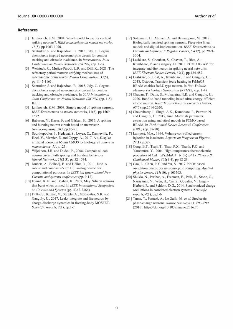
Fig. 15 shows two different implementations of a neuron
using RRAM. Previously, RRAM has been used as a
switching element only [19]-[20] (Fig. 15a). It has two
resistance states with which the electrical capacitor either
charges or discharges. In such neurons, the capacitor performs
integration with an electrical timescale. The RRAM switching
has its own timescale, which depends on the switching
mechanism, e.g., IMT or self-heating. The relatively longer
electrothermal RRAM switching timescales are proposed in
this paper to replace the large electrical capacitors for
integration functionality.
The electrothermal timescale from the 10𝛍m ×10𝛍m
RRAM is experimentally shown as 100ns-1𝛍s with a max
current of 10mA. To implement an electrical RC timescale,
assuming a 2nm thick SiO2 based capacitor of the same area
will produce capacitance of 1.7pF, which results in a time
constant of 0.1ns for a 1V threshold for firing. This is a 100-
1000x smaller timescale. For an equivalent timescale of
100ns-1𝛍s, a 100-1000x larger area capacitor is needed with
the same RRAM size to adversely affect area efficiency. As
devices scale, the electrical-time constant is largely area
independent – given by the following:
𝛕𝐑𝐂 =𝐂𝐕
𝐈= (
𝛜𝐀
𝐝)
𝐕
{𝐉𝐃𝐀}=
𝛜𝐕
𝐝𝐉𝐃
(𝟓)
Where 𝐂 is electrical capacitance which depends on
dielectric constant 𝛆, the thickness of insulator 𝐝, and
capacitor area 𝐀, 𝐕 is the threshold voltage, 𝐈 is charging
current through the RRAM, which depends on the switching
current density 𝐉𝐃 and area 𝐀 assumed to be the same as the
capacitor. The electrothermal timescale is also approximately
scaling independent and is given by the following:
𝛕𝐭𝐡 =𝐂𝐭𝐡𝚫𝐓
𝐇= 𝐂𝐯𝐀𝐋
𝚫𝐓
{𝐕𝐉𝐃 𝐀𝐋}= (𝐂𝐯)
𝚫𝐓
{𝐕𝐉𝐃} (𝟔)
Figure 12 Experimental Voltage Controlled Spiking
Frequency behaviour demonstrated. For (a) Vinput = -1.6V,
spiking frequency is 595 KHz while for (b) Vinput = -1.8V,
spiking frequency is 757 KHz. (c) Comparison of Spiking
Frequency vs Input voltage between experiments and
simulations
(a) (b)
(c)
Figure 13 Experimental Spiking Pattern for Time Varying
Input: Input voltage is combination of two-time varying
sinusoidal signals of equal magnitude and different
frequencies.
Figure 14 Experimental Spiking Patterns (a) Intrinsic
Bursting (b) Chattering
(a) (b)
Journal XX (XXXX) XXXXXX Author et al
9
Where 𝐂𝐭𝐡 is thermal capacitance, which depends upon
specific heat capacity 𝐂𝐯, area of device A, and the thickness
of the device, L, 𝚫𝐓 is a change in device temperature. So, the
ratio of the timescale benefit will remain approximately
constant. This largely sustains the large area efficiency with
scaling.
9. Conclusion
In summary, we demonstrate different spiking patterns of a
cortical neuron using a PMO RRAM-based neuron. The
benchmarking of the PMO-based neuron circuit is shown in
Table 2. In the proposed circuit, 6-bit register consisting of 6
flip flops, 1 OR gate, 2 switches, and 3 transistors for 1 resistor
will be used, with a total transistor count of 119, based on
which a feature size of 11.9 x10³ F2 is estimated. The neuron
implementation shown in this paper is capacitor-less as PMO
RRAM uses the internal self-heating timescales for integration
operation and hence eliminates the use of a capacitor. Unlike
previous demonstrations, an asynchronous simulation-based
analysis with the driving circuitry and electrothermal model of
the PMO RRAM device demonstrated realistic bursting
patterns. Experiments guided by simulations validate the
simulation results. With scalable PMO RRAM devices
integrated with digital components for the driving circuit, a
compact neuron can be designed, which is highly attractive for
large-scale SNNs.
Wijekoon
[8]
Joubert
[9]
Tuma
[21]
Dutta
[11]
Lashkare
[13]
Lashkare
[14]
Gao
[19]
Shukla
[20] This Work
Platform CMOS CMOS
Phase
Change
+
CMOS
SOI
CMOS
PCMO +
PMOS PMO + CMOS - - PMO + CMOS
Circuit
Type
Analog +
Asynch.
Digital +
Synch.
Mixed +
Synch.
Analog
+
Asynch.
Mixed +
Synch.
Mixed +
Asynch. - -
Mixed +
Asynch.
Neuron
Model LIF LIF IF LIF IF LIF LIF LIF LIF
Spiking
Behavior*
RS, FS,
IB, CH RS RS RS RS RS - - RS, IB, CH
Refractory
Period Fixed Fixed Fixed Fixed Fixed Fixed - - Control
Timescale
Generation Cap Cap -
Floating
Body
Effect
Gradual
Resistive
Switching
Electro-
thermal Cap Cap
Electro-
thermal
RRAM
Usage - - - - Integrator Integrator Switch Switch
Integrator,
Refractory
Period
Area
(×103 F2) 23 127 2551 1.767 3.086 - - - 11.908
Table 2: Benchmarking with Previous RRAM Implementations
*RS: Regular Spiking, FS: Fast Spiking
Figure 15 (a) RRAM based neuron where RRAM device
acts as a switching element and integration timescale is
controlled by the external capacitor, (b) Proposed RRAM
based neuron where RRAM device provides the
electrothermal integration timescale in addition to being a
switch.
(a) (b)
Journal XX (XXXX) XXXXXX Author et al
10
References
[1] Izhikevich, E.M., 2004. Which model to use for cortical
spiking neurons?. IEEE transactions on neural networks,
15(5), pp.1063-1070.
[2] Santurkar, S. and Rajendran, B., 2015, July. C. elegans
chemotaxis inspired neuromorphic circuit for contour
tracking and obstacle avoidance. In International Joint
Conference on Neural Networks (IJCNN) (pp. 1-8).
[3] Weistuch, C., Mujica-Parodi, L.R. and Dill, K., 2021. The
refractory period matters: unifying mechanisms of
macroscopic brain waves. Neural Computation, 33(5),
pp.1145-1163.
[4] Santurkar, S. and Rajendran, B., 2015, July. C. elegans
chemotaxis inspired neuromorphic circuit for contour
tracking and obstacle avoidance. In 2015 International
Joint Conference on Neural Networks (IJCNN) (pp. 1-8).
IEEE.
[5] Izhikevich, E.M., 2003. Simple model of spiking neurons.
IEEE Transactions on neural networks, 14(6), pp.1569-
1572.
[6] Babacan, Y., Kaçar, F. and Gürkan, K., 2016. A spiking
and bursting neuron circuit based on memristor.
Neurocomputing, 203, pp.86-91.
[7] Sourikopoulos, I., Hedayat, S., Loyez, C., Danneville, F.,
Hoel, V., Mercier, E. and Cappy, A., 2017. A 4-fJ/spike
artificial neuron in 65 nm CMOS technology. Frontiers in
neuroscience, 11, p.123.
[8] Wijekoon, J.H. and Dudek, P., 2008. Compact silicon
neuron circuit with spiking and bursting behaviour.
Neural Networks, 21(2-3), pp.524-534.
[9] Joubert, A., Belhadj, B. and Héliot, R., 2011, June. A
robust and compact 65 nm LIF analog neuron for
computational purposes. In IEEE 9th International New
Circuits and systems conference (pp. 9-12).
[10] Hynna, K.M. and Boahen, K., 2007, May. Silicon neurons
that burst when primed. In IEEE International Symposium
on Circuits and Systems (pp. 3363-3366).
[11] Dutta, S., Kumar, V., Shukla, A., Mohapatra, N.R. and
Ganguly, U., 2017. Leaky integrate and fire neuron by
charge-discharge dynamics in floating-body MOSFET.
Scientific reports, 7(1), pp.1-7.
[12] Soleimani, H., Ahmadi, A. and Bavandpour, M., 2012.
Biologically inspired spiking neurons: Piecewise linear
models and digital implementation. IEEE Transactions on
Circuits and Systems I: Regular Papers, 59(12), pp.2991-
3004.
[13] Lashkare, S., Chouhan, S., Chavan, T., Bhat, A.,
Kumbhare, P. and Ganguly, U., 2018. PCMO RRAM for
integrate-and-fire neuron in spiking neural networks.
IEEE Electron Device Letters, 39(4), pp.484-487.
[14] Lashkare, S., Bhat, A., Kumbhare, P. and Ganguly, U.,
2018, October. Transient joule heating in PrMnO3
RRAM enables ReLU type neuron. In Non-Volatile
Memory Technology Symposium (NVMTS) (pp. 1-4).
[15] Chavan, T., Dutta, S., Mohapatra, N.R. and Ganguly, U.,
2020. Band-to-band tunneling based ultra-energy-efficient
silicon neuron. IEEE Transactions on Electron Devices,
67(6), pp.2614-2620.
[16] Chakraborty, I., Singh, A.K., Kumbhare, P., Panwar, N.
and Ganguly, U., 2015, June. Materials parameter
extraction using analytical models in PCMO based
RRAM. In 73rd Annual Device Research Conference
(DRC) (pp. 87-88).
[17] Lampert, M.A., 1964. Volume-controlled current
injection in insulators. Reports on Progress in Physics,
27(1), p.329.
[18] Cong, B.T., Tsuji, T., Thao, P.X., Thanh, P.Q. and
Yamamura, Y., 2004. High-temperature thermoelectric
properties of Ca1− xPrxMnO3− δ (0⩽ x< 1). Physica B:
Condensed Matter, 352(1-4), pp.18-23.
[19] Gao, L., Chen, P.Y. and Yu, S., 2017. NbOx based
oscillation neuron for neuromorphic computing. Applied
physics letters, 111(10), p.103503.
[20] Shukla, N., Parihar, A., Freeman, E., Paik, H., Stone, G.,
Narayanan, V., Wen, H., Cai, Z., Gopalan, V., Engel-
Herbert, R. and Schlom, D.G., 2014. Synchronized charge
oscillations in correlated electron systems. Scientific
reports, 4(1), pp.1-6.
[21] Tuma, T., Pantazi, A., Le Gallo, M. et al. Stochastic
phase-change neurons. Nature Nanotech 11, 693–699
(2016). https://doi.org/10.1038/nnano.2016.70