Embed Size (px)
Citation preview
Exploiting Design-for-Debug for Flexible SoC SecurityArchitecture
Abhishek BasakDept. of EECS
Case Western Reserve Univ.Cleveland, OH, USA
Swarup BhuniaDept. of ECE
University of FloridaGainesville, FL, USA
Sandip RayStrategic CAD Labs
Intel CorporationHillsboro, OR, USA
ABSTRACTSystematic implementation of System-on-Chip (SoC) secu-rity policies typically involves smart wrappers extracting lo-cal security critical events of interest from Intellectual Prop-erty (IP) blocks, together with a control engine that com-municates with the wrappers to analyze the events for pol-icy adherence. However, developing customized wrappersat each IP for security requirements may incur significantoverhead in area and hardware resources. In this paper, weaddress this problem by exploiting the extensive design-for-debug (DfD) instrumentation already available on-chip. Inaddition to reduction in the overall hardware overhead, theapproach also adds flexibility to the security architecture it-self, e.g., permitting use of on-field DfD instrumentation,survivability and control hooks to patch security policy im-plementation in response to bugs and attacks found at post-silicon or changing security requirements on-field. We showhow to design scalable interface between security and debugarchitectures that provides the benefits of flexibility to secu-rity policy implementation without interfering with existingdebug and survivability use cases and at minimal additionalcost in energy and design complexity.
1. INTRODUCTIONToday’s embedded and mobile systems contain a signif-
icant amount of sensitive information and data (often col-lectively referred to as assets) that must be protected fromunauthorized access. Such assets include private end-userinformation, cryptographic and DRM keys, firmware, de-bug and control modes, defeaturing bits, etc. Consequently,most system design specifications include a number of secu-rity policies [1, 2, 3] that define access constraints to theseassets at different phases in the system execution. In cur-rent industrial System-on-Chip (SoC) design development,these policies are defined at different phases of design explo-ration, planning, and development by system architects aswell as different IP and SoC integration teams, and often getrefined or updated across the system development and val-
Permission to make digital or hard copies of all or part of this work for personal orclassroom use is granted without fee provided that copies are not made or distributedfor profit or commercial advantage and that copies bear this notice and the full cita-tion on the first page. Copyrights for components of this work owned by others thanACM must be honored. Abstracting with credit is permitted. To copy otherwise, or re-publish, to post on servers or to redistribute to lists, requires prior specific permissionand/or a fee. Request permissions from [email protected].
DAC ’16, June 05-09, 2016, Austin, TX, USAc© 2016 ACM. ISBN 978-1-4503-4236-0/16/06. . . $15.00
DOI: http://dx.doi.org/10.1145/2897937.2898020
idation phases. Unfortunately, the policies are highly sub-tle, involving multiple IPs and complex hardware, firmwareand software interactions. Their implementations are inter-twined with the implementation of the system functionalitythrough a combination of RTL, firmware, or software com-ponents. Consequently, it is challenging to validate systemadherence against a set of policies, or update the policiesthemselves post production, e.g., in response to changingcustomer needs or newly identified attack scenarios.
Previous work attempted to address this problem by de-veloping a flexible and generic security architecture for im-plementing SoC security policies [4, 5]. The architectureconstitutes a centralized control engine programmed withthe restrictions imposed by the various security policies. Thesystem was shown to be flexible for implementing diverse se-curity policies, including access control, time-of-check time-of-use (TOCTOU), and system boot policies. However, thearchitecture required each individual IP in the SoC to beaugmented with a wrapper customized for security require-ments; the wrappers identified the security-relevant events,communications, and data in the IP and coordinated withthe centralized controller to ensure policy adherence. Ina SoC design containing a large number of IPs, the costincurred by such approach in terms of area overhead anddesign complexity may be prohibitive.
The key insight of this paper is that we can implementa security policy control system without incurring signifi-cant additional architecture and design overhead, by exploit-ing infrastructures already available on-chip. In particular,modern SoC designs contain a significant amount of Design-for-Debug (DfD) features to enable observability and con-trol of the design execution during post-silicon debug andvalidation, and provide means to “patch” the design in re-sponse to errors or vulnerabilities found on-field. On theother hand, usage of this instrumentation post production,i.e., for on-field debug and error mitigation, is sporadic andrare. Consequently, computing systems have a significantamount of mature hardware infrastructure for control andobservability of internal events, that is available and unusedduring normal system usages.
Our main contribution is a flexible architecture that ex-ploits on-chip DfD features for implementing SoC securitypolicies. We show how to build efficient, low-overhead se-curity wrappers by re-purposing the debug infrastructure,while being transparent to debug and validation usages. Weillustrate some of the design trade-offs involved betweencomplexity, transparency needs, and energy efficiency. Ourexperimental results on a SoC design with illustrative DfD

Figure 1: Simplified SoC DfD Architecture Basedon CoresightTM.
instrumentation shows that the approach could potentiallyprovide significant savings in area and hardware overheadwhile permitting flexibility in on-field adaptation of securitypolicies over a dedicated wrapper implementation, withoutsignificant increase in power/energy consumption.
The remainder of the paper is organized as follows. Sec-tion 2 provides the relevant background on DfD features,SoC security policies, and security architecture. Section 3identifies the constraints involved in re-purposing DfD fea-tures. Section 4 describes some key components of our pro-posed security architecture. Section 5 defines some illustra-tive use cases. We provide experimental results on the over-head of the architecture in Section 6, discuss related workin Section 7, and conclude in Section 8.
2. BACKGROUND
2.1 On-Chip Debug InfrastructureDesign-for-Debug (DfD) refers to on-chip hardware for fa-
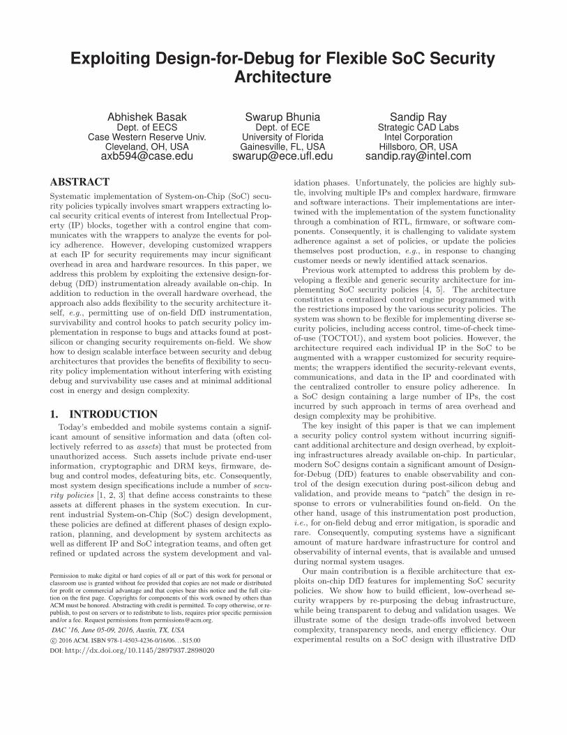
cilitating post-silicon validation [6]. A key requirement forpost-silicon validation is observability and controllability ofinternal signals during silicon execution. DfD in modernSoC designs include facilities to trace critical hardware sig-nals, dump contents of registers and memory arrays, patchmicrocode and firmware, create user-defined triggers and in-terrupts, etc. Furthermore, DfD architecture is increasinglygetting standardized to enable third-party EDA vendors tocreate software APIs for accessing and controlling the hard-ware instrumentation for system-level debug. As an exam-ple, ARM CoresightTM architecture [7] (Fig. 1) provides fa-cilities for tracing, synchronization, and time-stamping hard-ware and software events, a trigger logic, and facilities forstandardized DfD access and trace transport. The architec-ture is instantiated into Macrocells that can interact with IPfunctionality through standard interfaces. Debug interfaceis used not only for post-silicon but to enable workaroundsfor bugs and defects found on-field.
2.2 Security Policies and Security ArchitectureSecurity policies govern access to sensitive assets in a SoC
design. Following are two illustrative policies: [1, 4, 8]
1. During boot, keys transmitted by the crypto enginecannot be observed by any IP other than its intendedtarget.
2. An on-chip fuse can be updated for silicon validationbut not after production.
Previous work [4] defined a security architecture, called “E-IIPS”for disciplined, systematic implementation of such poli-cies. The architecture includes a central security policy con-troller (SPC) that keeps track of the system security stateand enforces the restrictions imposed by the policies in thatstate. SPC communicates with security wrappers for indi-vidual IP blocks that detect security critical events from IPoperations.
3. DFD RE-PURPOSING CONSTRAINTSDfD is a complex component of SoC design, that is de-
veloped to cater to the needs of validation, debug, and on-field workarounds. In this section we summarize some of theconstraints and requirements that must be satisfied while re-purposing this architecture for security.
Transparency to Debug Use Cases. Post-silicon debugand validation are themselves critical activities performedunder highly aggressive schedules. It is therefore criticalthat re-purposing the DfD does not interfere or “compete”with debug usages of the same hardware. For instance, ifa trace or trigger module is necessary for a debug usage,then it cannot be simultaneously used for enforcing securityconstraints.
Maintaining Power-Performance Profile. On-chip in-strumentation is optimized for energy and performance inusages related to debug. For example, since debug trafficis typically ”bursty”, it is possible to incur low penalty inpower consumption even with a high-bandwidth fabric bypower-gating the fabric components during normal execu-tion; while re-purposing the same infrastructure, one mustensure that the power profile is not significantly disruptedby the new usages.
Acceptable Overhead for Interfacing Hardware. Akey motivation for exploiting DfD for security architecture isreducing hardware overhead. However, this benefit would beobviously lost if significant hardware is necessary to interfacewith the DfD and configure it for security needs.
4. DFD-BASED SECURITY ARCHITECTUREOur architecture is built on top of the E-IIPS frame-
work [4]. We exploit DfD to implement smart security wrap-pers for IPs that communicate with the centralized policycontroller (SPC), which implements security policies. Fur-thermore, SPC can program DfD to implement security con-trols using logic available for on-field upgrades.
4.1 Detection of Security-Critical EventsTo avoid potential routing bottlenecks due to high band-
width requirements, IP security wrappers must detect a setof security-critical events. The events necessary are basedon the policy as well as the IP involved, e.g., for a CPUwe need to detect attempts of privilege escalation and mon-itor control flow of programs to detect probable presence ofmalware as well as prevent fine-grained timing based mas-querading attacks. Developing IP security wrappers thus re-
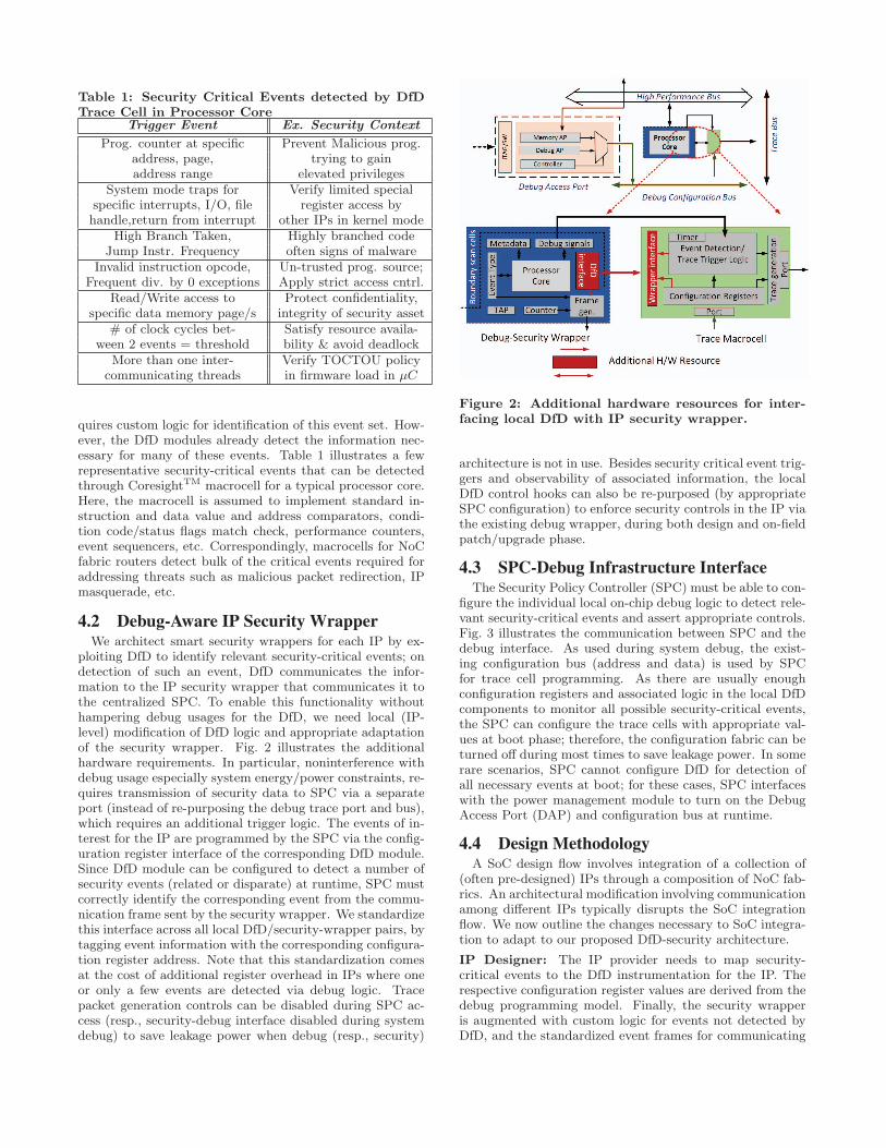
Table 1: Security Critical Events detected by DfDTrace Cell in Processor Core
Trigger Event Ex. Security Context
Prog. counter at specific Prevent Malicious prog.address, page, trying to gainaddress range elevated privileges
System mode traps for Verify limited specialspecific interrupts, I/O, file register access byhandle,return from interrupt other IPs in kernel mode
High Branch Taken, Highly branched codeJump Instr. Frequency often signs of malware
Invalid instruction opcode, Un-trusted prog. source;Frequent div. by 0 exceptions Apply strict access cntrl.
Read/Write access to Protect confidentiality,specific data memory page/s integrity of security asset
# of clock cycles bet- Satisfy resource availa-ween 2 events = threshold bility & avoid deadlock
More than one inter- Verify TOCTOU policycommunicating threads in firmware load in μC
quires custom logic for identification of this event set. How-ever, the DfD modules already detect the information nec-essary for many of these events. Table 1 illustrates a fewrepresentative security-critical events that can be detectedthrough CoresightTM macrocell for a typical processor core.Here, the macrocell is assumed to implement standard in-struction and data value and address comparators, condi-tion code/status flags match check, performance counters,event sequencers, etc. Correspondingly, macrocells for NoCfabric routers detect bulk of the critical events required foraddressing threats such as malicious packet redirection, IPmasquerade, etc.
4.2 Debug-Aware IP Security WrapperWe architect smart security wrappers for each IP by ex-
ploiting DfD to identify relevant security-critical events; ondetection of such an event, DfD communicates the infor-mation to the IP security wrapper that communicates it tothe centralized SPC. To enable this functionality withouthampering debug usages for the DfD, we need local (IP-level) modification of DfD logic and appropriate adaptationof the security wrapper. Fig. 2 illustrates the additionalhardware requirements. In particular, noninterference withdebug usage especially system energy/power constraints, re-quires transmission of security data to SPC via a separateport (instead of re-purposing the debug trace port and bus),which requires an additional trigger logic. The events of in-terest for the IP are programmed by the SPC via the config-uration register interface of the corresponding DfD module.Since DfD module can be configured to detect a number ofsecurity events (related or disparate) at runtime, SPC mustcorrectly identify the corresponding event from the commu-nication frame sent by the security wrapper. We standardizethis interface across all local DfD/security-wrapper pairs, bytagging event information with the corresponding configura-tion register address. Note that this standardization comesat the cost of additional register overhead in IPs where oneor only a few events are detected via debug logic. Tracepacket generation controls can be disabled during SPC ac-cess (resp., security-debug interface disabled during systemdebug) to save leakage power when debug (resp., security)
Figure 2: Additional hardware resources for inter-facing local DfD with IP security wrapper.
architecture is not in use. Besides security critical event trig-gers and observability of associated information, the localDfD control hooks can also be re-purposed (by appropriateSPC configuration) to enforce security controls in the IP viathe existing debug wrapper, during both design and on-fieldpatch/upgrade phase.
4.3 SPC-Debug Infrastructure InterfaceThe Security Policy Controller (SPC) must be able to con-
figure the individual local on-chip debug logic to detect rele-vant security-critical events and assert appropriate controls.Fig. 3 illustrates the communication between SPC and thedebug interface. As used during system debug, the exist-ing configuration bus (address and data) is used by SPCfor trace cell programming. As there are usually enoughconfiguration registers and associated logic in the local DfDcomponents to monitor all possible security-critical events,the SPC can configure the trace cells with appropriate val-ues at boot phase; therefore, the configuration fabric can beturned off during most times to save leakage power. In somerare scenarios, SPC cannot configure DfD for detection ofall necessary events at boot; for these cases, SPC interfaceswith the power management module to turn on the DebugAccess Port (DAP) and configuration bus at runtime.
4.4 Design MethodologyA SoC design flow involves integration of a collection of
(often pre-designed) IPs through a composition of NoC fab-rics. An architectural modification involving communicationamong different IPs typically disrupts the SoC integrationflow. We now outline the changes necessary to SoC integra-tion to adapt to our proposed DfD-security architecture.
IP Designer: The IP provider needs to map security-critical events to the DfD instrumentation for the IP. Therespective configuration register values are derived from thedebug programming model. Finally, the security wrapperis augmented with custom logic for events not detected byDfD, and the standardized event frames for communicating
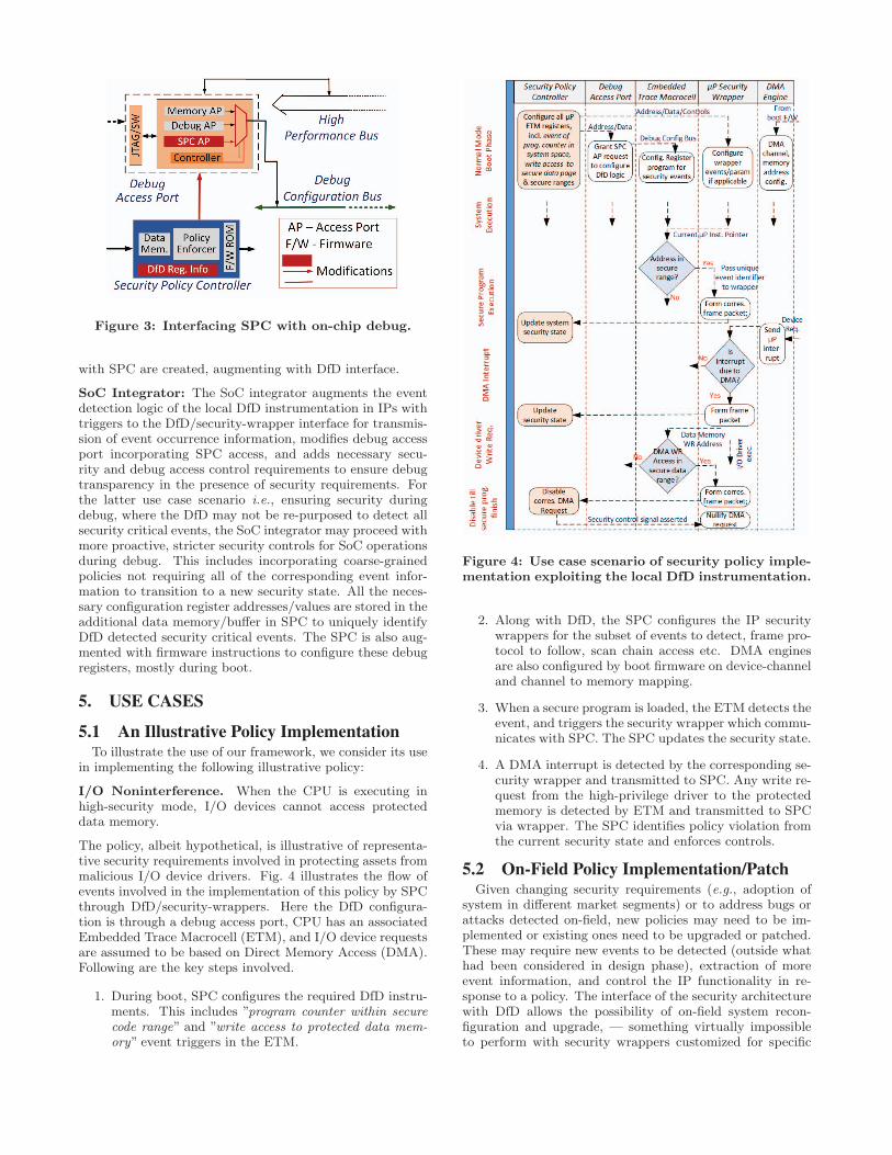
Figure 3: Interfacing SPC with on-chip debug.
with SPC are created, augmenting with DfD interface.
SoC Integrator: The SoC integrator augments the eventdetection logic of the local DfD instrumentation in IPs withtriggers to the DfD/security-wrapper interface for transmis-sion of event occurrence information, modifies debug accessport incorporating SPC access, and adds necessary secu-rity and debug access control requirements to ensure debugtransparency in the presence of security requirements. Forthe latter use case scenario i.e., ensuring security duringdebug, where the DfD may not be re-purposed to detect allsecurity critical events, the SoC integrator may proceed withmore proactive, stricter security controls for SoC operationsduring debug. This includes incorporating coarse-grainedpolicies not requiring all of the corresponding event infor-mation to transition to a new security state. All the neces-sary configuration register addresses/values are stored in theadditional data memory/buffer in SPC to uniquely identifyDfD detected security critical events. The SPC is also aug-mented with firmware instructions to configure these debugregisters, mostly during boot.
5. USE CASES
5.1 An Illustrative Policy ImplementationTo illustrate the use of our framework, we consider its use
in implementing the following illustrative policy:
I/O Noninterference. When the CPU is executing inhigh-security mode, I/O devices cannot access protecteddata memory.
The policy, albeit hypothetical, is illustrative of representa-tive security requirements involved in protecting assets frommalicious I/O device drivers. Fig. 4 illustrates the flow ofevents involved in the implementation of this policy by SPCthrough DfD/security-wrappers. Here the DfD configura-tion is through a debug access port, CPU has an associatedEmbedded Trace Macrocell (ETM), and I/O device requestsare assumed to be based on Direct Memory Access (DMA).Following are the key steps involved.
1. During boot, SPC configures the required DfD instru-ments. This includes ”program counter within securecode range” and ”write access to protected data mem-ory” event triggers in the ETM.
Figure 4: Use case scenario of security policy imple-mentation exploiting the local DfD instrumentation.
2. Along with DfD, the SPC configures the IP securitywrappers for the subset of events to detect, frame pro-tocol to follow, scan chain access etc. DMA enginesare also configured by boot firmware on device-channeland channel to memory mapping.
3. When a secure program is loaded, the ETM detects theevent, and triggers the security wrapper which commu-nicates with SPC. The SPC updates the security state.
4. A DMA interrupt is detected by the corresponding se-curity wrapper and transmitted to SPC. Any write re-quest from the high-privilege driver to the protectedmemory is detected by ETM and transmitted to SPCvia wrapper. The SPC identifies policy violation fromthe current security state and enforces controls.
5.2 On-Field Policy Implementation/PatchGiven changing security requirements (e.g., adoption of
system in different market segments) or to address bugs orattacks detected on-field, new policies may need to be im-plemented or existing ones need to be upgraded or patched.These may require new events to be detected (outside whathad been considered in design phase), extraction of moreevent information, and control the IP functionality in re-sponse to a policy. The interface of the security architecturewith DfD allows the possibility of on-field system recon-figuration and upgrade, — something virtually impossibleto perform with security wrappers customized for specific
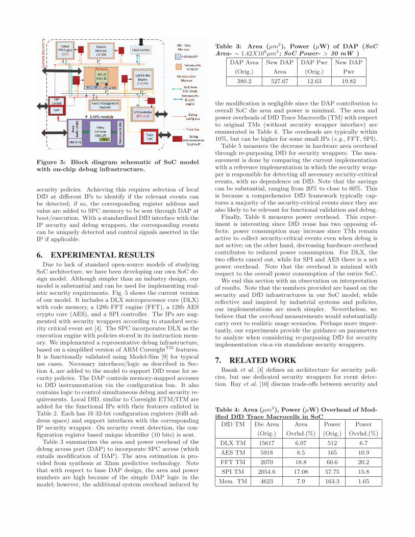
Figure 5: Block diagram schematic of SoC modelwith on-chip debug infrastructure.
security policies. Achieving this requires selection of localDfD at different IPs to identify if the relevant events canbe detected; if so, the corresponding register address andvalue are added to SPC memory to be sent through DAP atboot/execution. With a standardized DfD interface with theIP security and debug wrappers, the corresponding eventscan be uniquely detected and control signals asserted in theIP if applicable.
6. EXPERIMENTAL RESULTSDue to lack of standard open-source models of studying
SoC architecture, we have been developing our own SoC de-sign model. Although simpler than an industry design, ourmodel is substantial and can be used for implementing real-istic security requirements. Fig. 5 shows the current versionof our model. It includes a DLX microprocessor core (DLX)with code memory, a 128b FFT engine (FFT), a 128b AEScrypto core (AES), and a SPI controller. The IPs are aug-mented with security wrappers according to standard secu-rity critical event set [4]. The SPC incorporates DLX as theexecution engine with policies stored in its instruction mem-ory. We implemented a representative debug infrastructure,based on a simplified version of ARM CoresightTM features.It is functionally validated using Model-Sim [9] for typicaluse cases. Necessary interfaces/logic as described in Sec-tion 4, are added to the model to support DfD reuse for se-curity policies. The DAP controls memory-mapped accessesto DfD instrumentation via the configuration bus. It alsocontains logic to control simultaneous debug and security re-quirements. Local DfD, similar to Coresight ETM/ITM areadded for the functional IPs with their features enlisted inTable 2. Each has 16 32-bit configuration registers (64B ad-dress space) and support interfaces with the correspondingIP security wrapper. On security event detection, the con-figuration register based unique identifier (10 bits) is sent.
Table 3 summarizes the area and power overhead of thedebug access port (DAP) to incorporate SPC access (whichentails modification of DAP). The area estimation is pro-vided from synthesis at 32nm predictive technology. Notethat with respect to base DAP design, the area and powernumbers are high because of the simple DAP logic in themodel; however, the additional system overhead induced by
Table 3: Area (μm2), Power (μW) of DAP (SoCArea- ∼ 1.42X106μm2; SoC Power- > 30 mW )
DAP Area New DAP DAP Pwr New DAP
(Orig.) Area (Orig.) Pwr
380.2 527.67 12.63 19.82
the modification is negligible since the DAP contribution tooverall SoC die area and power is minimal. The area andpower overheads of DfD Trace Macrocells (TM) with respectto original TMs (without security wrapper interface) areenumerated in Table 4. The overheads are typically within10%, but can be higher for some small IPs (e.g., FFT, SPI).
Table 5 measures the decrease in hardware area overheadthrough re-purposing DfD for security wrappers. The mea-surement is done by comparing the current implementationwith a reference implementation in which the security wrap-per is responsible for detecting all necessary security-criticalevents, with no dependence on DfD. Note that the savingscan be substantial, ranging from 20% to close to 60%. Thisis because a comprehensive DfD framework typically cap-tures a majority of the security-critical events since they arealso likely to be relevant for functional validation and debug.
Finally, Table 6 measures power overhead. This exper-iment is interesting since DfD reuse has two opposing ef-fects: power consumption may increase since TMs remainactive to collect security-critical events even when debug isnot active; on the other hand, decreasing hardware overheadcontributes to reduced power consumption. For DLX, thetwo effects cancel out, while for SPI and AES there is a netpower overhead. Note that the overhead is minimal withrespect to the overall power consumption of the entire SoC.
We end this section with an observation on interpretationof results. Note that the numbers provided are based on thesecurity and DfD infrastructures in our SoC model; whilereflective and inspired by industrial systems and policies,our implementations are much simpler. Nevertheless, webelieve that the overhead measurements would substantiallycarry over to realistic usage scenarios. Perhaps more impor-tantly, our experiments provide the guidance on parametersto analyze when considering re-purposing DfD for securityimplementation vis-a-vis standalone security wrappers.
7. RELATED WORKBasak et al. [4] defines an architecture for security poli-
cies, but use dedicated security wrappers for event detec-tion. Ray et al. [10] discuss trade-offs between security and
Table 4: Area (μm2), Power (μW) Overhead of Mod-ified DfD Trace Macrocells in SoCDfD TM Die Area Area Power Power
(Orig.) Ovrhd.(%) (Orig.) Ovrhd.(%)
DLX TM 15617 6.07 512 6.7
AES TM 5918 8.5 165 10.9
FFT TM 2070 18.8 60.6 20.2
SPI TM 2054.6 17.08 57.75 15.8
Mem. TM 4623 7.9 163.3 1.65
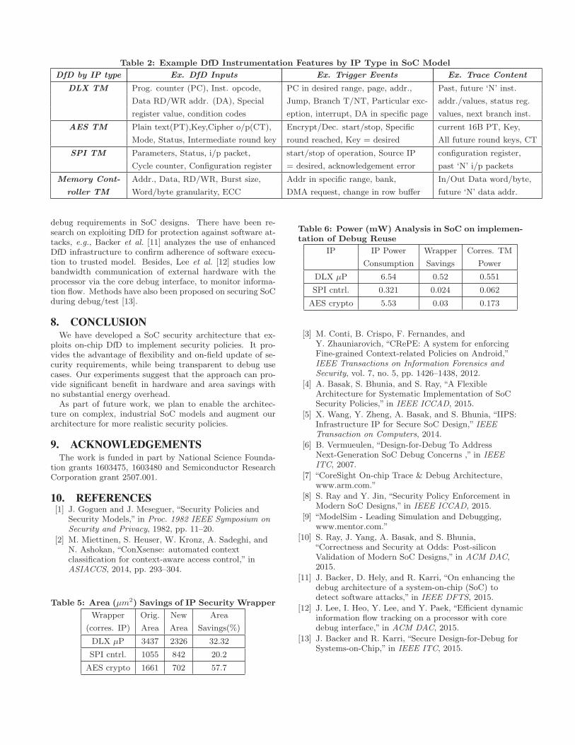
Table 2: Example DfD Instrumentation Features by IP Type in SoC Model
DfD by IP type Ex. DfD Inputs Ex. Trigger Events Ex. Trace Content
DLX TM Prog. counter (PC), Inst. opcode, PC in desired range, page, addr., Past, future ‘N’ inst.
Data RD/WR addr. (DA), Special Jump, Branch T/NT, Particular exc- addr./values, status reg.
register value, condition codes eption, interrupt, DA in specific page values, next branch inst.
AES TM Plain text(PT),Key,Cipher o/p(CT), Encrypt/Dec. start/stop, Specific current 16B PT, Key,
Mode, Status, Intermediate round key round reached, Key = desired All future round keys, CT
SPI TM Parameters, Status, i/p packet, start/stop of operation, Source IP configuration register,
Cycle counter, Configuration register = desired, acknowledgement error past ‘N’ i/p packets
Memory Cont- Addr., Data, RD/WR, Burst size, Addr in specific range, bank, In/Out Data word/byte,
roller TM Word/byte granularity, ECC DMA request, change in row buffer future ‘N’ data addr.
debug requirements in SoC designs. There have been re-search on exploiting DfD for protection against software at-tacks, e.g., Backer et al. [11] analyzes the use of enhancedDfD infrastructure to confirm adherence of software execu-tion to trusted model. Besides, Lee et al. [12] studies lowbandwidth communication of external hardware with theprocessor via the core debug interface, to monitor informa-tion flow. Methods have also been proposed on securing SoCduring debug/test [13].
8. CONCLUSIONWe have developed a SoC security architecture that ex-
ploits on-chip DfD to implement security policies. It pro-vides the advantage of flexibility and on-field update of se-curity requirements, while being transparent to debug usecases. Our experiments suggest that the approach can pro-vide significant benefit in hardware and area savings withno substantial energy overhead.
As part of future work, we plan to enable the architec-ture on complex, industrial SoC models and augment ourarchitecture for more realistic security policies.
9. ACKNOWLEDGEMENTSThe work is funded in part by National Science Founda-
tion grants 1603475, 1603480 and Semiconductor ResearchCorporation grant 2507.001.
10. REFERENCES[1] J. Goguen and J. Meseguer, “Security Policies and
Security Models,” in Proc. 1982 IEEE Symposium onSecurity and Privacy, 1982, pp. 11–20.
[2] M. Miettinen, S. Heuser, W. Kronz, A. Sadeghi, andN. Ashokan, “ConXsense: automated contextclassification for context-aware access control,” inASIACCS, 2014, pp. 293–304.
Table 5: Area (μm2) Savings of IP Security Wrapper
Wrapper Orig. New Area
(corres. IP) Area Area Savings(%)
DLX μP 3437 2326 32.32
SPI cntrl. 1055 842 20.2
AES crypto 1661 702 57.7
Table 6: Power (mW) Analysis in SoC on implemen-tation of Debug Reuse
IP IP Power Wrapper Corres. TM
Consumption Savings Power
DLX μP 6.54 0.52 0.551
SPI cntrl. 0.321 0.024 0.062
AES crypto 5.53 0.03 0.173
[3] M. Conti, B. Crispo, F. Fernandes, andY. Zhauniarovich, “CRePE: A system for enforcingFine-grained Context-related Policies on Android,”IEEE Transactions on Information Forensics andSecurity, vol. 7, no. 5, pp. 1426–1438, 2012.
[4] A. Basak, S. Bhunia, and S. Ray, “A FlexibleArchitecture for Systematic Implementation of SoCSecurity Policies,” in IEEE ICCAD, 2015.
[5] X. Wang, Y. Zheng, A. Basak, and S. Bhunia, “IIPS:Infrastructure IP for Secure SoC Design,” IEEETransaction on Computers, 2014.
[6] B. Vermueulen, “Design-for-Debug To AddressNext-Generation SoC Debug Concerns ,” in IEEEITC, 2007.
[7] “CoreSight On-chip Trace & Debug Architecture,www.arm.com.”
[8] S. Ray and Y. Jin, “Security Policy Enforcement inModern SoC Designs,” in IEEE ICCAD, 2015.
[9] “ModelSim - Leading Simulation and Debugging,www.mentor.com.”
[10] S. Ray, J. Yang, A. Basak, and S. Bhunia,“Correctness and Security at Odds: Post-siliconValidation of Modern SoC Designs,” in ACM DAC,2015.
[11] J. Backer, D. Hely, and R. Karri, “On enhancing thedebug architecture of a system-on-chip (SoC) todetect software attacks,” in IEEE DFTS, 2015.
[12] J. Lee, I. Heo, Y. Lee, and Y. Paek, “Efficient dynamicinformation flow tracking on a processor with coredebug interface,” in ACM DAC, 2015.
[13] J. Backer and R. Karri, “Secure Design-for-Debug forSystems-on-Chip,” in IEEE ITC, 2015.


![Advanced(Debug(for(( ((SOC(Verificaon(Tutorial - … · Advanced(Debug(for((((SOC(Verificaon (Tutorial ([Indago™(Debug(Plaorm(Overview]! Debugging(Con6nues(to(be(the(Most Time(Consuming(Effortby(50%(!](https://img.pdfslide.us/doc/110x75/5b4dbe207f8b9a0d2d8baeb8/advanceddebugfor-socvericaontutorial-advanceddebugforsocvericaon.jpg)