Embed Size (px)
Citation preview
Experiments with a Single BoardComputer (SBC)
ECE 395 MicroprocessorLaboratory
Version 1.41
Dr. Sol Rosenstark
Department of Electrical and Computer EngineeringNew Jersey Institute of Technology
Newark, New Jersey
c© 2007New Jersey Institute of Technology
All rights reserved

Contents
Changes in this Laboratory . . . . . . . . . . . . . . . . . . . . . . . . iiAcknowledgements . . . . . . . . . . . . . . . . . . . . . . . . . . . . . ii
Introduction 1General Objectives of this Laboratory . . . . . . . . . . . . . . . . . . 2References . . . . . . . . . . . . . . . . . . . . . . . . . . . . . . . . . . 2
Explanation of the µProcessor Board Design 4The Motorola MC68EC000 CPU . . . . . . . . . . . . . . . . . . . . . 4The 28C256 32 kbyte EEPROM . . . . . . . . . . . . . . . . . . . . . . 5The 62256 32-kbyte RAM . . . . . . . . . . . . . . . . . . . . . . . . . 5The 74LS138 3 to 8-line Decoder . . . . . . . . . . . . . . . . . . . . . 5The Serial Port Interface Chips . . . . . . . . . . . . . . . . . . . . . . 5The Parallel Port Interface Chips . . . . . . . . . . . . . . . . . . . . . 6The System Clock . . . . . . . . . . . . . . . . . . . . . . . . . . . . . 6The Reset Circuit . . . . . . . . . . . . . . . . . . . . . . . . . . . . . 7Decoding of the RD and WR signals . . . . . . . . . . . . . . . . . . . 8Supplying the DTACK Response . . . . . . . . . . . . . . . . . . . . . 8
The I8251A Programmable Communication Interface 9
The EEPROM Monitor Program 13
Parts List 15
Completing the Assembly of the SBC 17
Interfacing the SBC to a Personal Computer 19
Future Uses of the SBC 20
The Experiments 21Experiment 1 - Acquiring and Completing the SBC . . . . . . . . . . . 21Experiment 2 - Developing Software for the SBC . . . . . . . . . . . . 22
i

Experiment 3 — An Event Driven Annunciator System . . . . . . . . 24Experiment 4 — Testing and Simulating Some ICs . . . . . . . . . . . 27Experiment 5 — Testing the Serial Port . . . . . . . . . . . . . . . . . 28Experiment 6 — DAC Interface with the SBC . . . . . . . . . . . . . . 30Experiment 7 — The Logic Analyzer . . . . . . . . . . . . . . . . . . . 32
Appendix A — Optional Parallel Port Expansion 35
Changes in this Laboratory
The assembler and emulator that is offered by Antonakos is a perfectly workabledevelopment system. Those two programs have to be executed in DOS. Moststudents have difficulty mastering the intricacies of the DOS operating system.Accordingly it is recommended that students download the freely distributedand open EASy68K Development System. This system is windows oriented andit should be easy to become familiar with it.
The EASy68K emulator does not use Antonakos’s TRAP #0, TRAP #1,TRAP #3 and TRAP #9 for performing a variety of tasks. It implements agreater variety of tasks using only the TRAP #15 exception. The new version3.00 of the monitor program was modified to be compatible with the EASy68Kemulator. It makes the SBC capable of executing the EASy68K TRAP #15tasks 0–2, 4–7, 9 and 12–14. For a complete description consult my ECE252Supplementary Notes.
Acknowledgements
The students who finished their projects in the Spring of 1997 helped correctthe design as well as compile the parts list. Among them I would like to thankVinnie Cascio, Aamish Kapadia, Leo Hendriks and Dave Harrison. The latterwas also instrumental in modifying Antonakos’s monitor so it would functioncorrectly with this design. In addition I would like to thank Eric Staub andCraig Budinich for lending me their boards so that I could spend the 1997 end-of-year semester-break to thoroughly rewrite the monitor and add the featureswhich I think a good monitor requires. I would like to express my appreciationto Idan Mandelbaum for testing out the design with the MC68EC000 chip whichneeded to supplant the, now defunct, MC68008 originally used in this design.
Dave Harrison should be thanked additionally for testing the design de-scribed in this manual and for later adding a disassembler to the monitor, arather challenging task.
ii
Introduction
Since their invention in 1971, microprocessors have been used in the design of allkinds of electrical and other equipment. It is well known that most microwaveovens use microprocessors to read the input keypad and translate this intosignals to control the on-time as well as the power of the magnetron, which isthe device that supplies the energy used in cooking the food. That is a relativelymodern application of microprocessors. In cases of older designs, microprocessordevices replace troublesome mechanical systems. An example of this is foundin the ignition system of a modern automobile.
In the good old days, the spark distributor contained centrifugal weightsas well as a vacuum diaphragm device to control the ignition spark-advanceneeded at various engine speeds and loads. This method was very imprecise.Under certain climactic conditions, the spark advance weights got glued in placethrough the congealing of the very lubricant that was supposed to promotetheir movement. Vacuum diaphragms punctured with age. This represented amaintenance headache, not to mention the fact that the spark advance curvewas limited in the degrees of freedom that could be incorporated into its design.
In a modern vehicle the entire spark advance operation is taken care ofby a microprocessor device. There are two electromechanical transduces toinform the microprocessor of the crankshaft and camshaft position. In additionthere is data from a throttle position sensor, a mass air flow sensor, an oxygensensor as well as others too numerous to mention. Using the input data, themicroprocessor determines, through a well designed program, the spark timingrequired. Not only does this design eliminate a number of unreliable mechanicaldevices, but the efficacy of this design is further enhanced by the fact that thesoftware can be readily modified if it is desired to change the engine operatingcharacteristics. The use of microprocessors thus gives unprecedented flexibilityto the engine designer.
It should now be apparent from the above discussion that a microprocessordevice uses more than just software. To be useful, it must be interfaced to thereal world. It must act on externally gathered data and control the action ofsome device.
1

General Objectives of this Laboratory
It is the objective of this laboratory to give the students the opportunity toacquire some hands-on experience with the various workings of a microproces-sor. To attain that familiarity, all students will acquire an individual printedcircuit board (PCB) version of a microprocessor based single board computer(SBC). After adding a few components and populating the board with chips,they will make it operational by programming an EEPROM with the latestMonitor program. This SBC will have adequate interfacing capabilities to en-able the students to perform some useful input/output tasks. Programming ofthe device will be done in assembly language. Programming in a higher levellanguage would prevent the user from becoming intimately familiar with themicroprocessor.
This laboratory is intended to help educate engineers rather than computerscientists. As a consequence, some of the experiments described in this manualdeal with software and some deal with interfacing. This is to reinforce the ideadiscussed in the introduction, that a microprocessor is not of much use if it isnot interfaced to the real world.
References
The students should have the first reference listed below from a previous course.The other references are suggested, and may be helpful, but are not absolutelyessential.
• James L. Antonakos, The 68000 Microprocessor, Hardware and SoftwarePrinciples and Applications, Fifth Edition, Prentice Hall, 2004. Since itis used as a textbook in our microprocessor course, every student takingthis laboratory should have a copy.
• Intel Manual, or spec-sheet, for the I8251A PCI (Programmable Commu-nication Interface).
2

D0
D1
D3
D2
D4
D5
D6
D7
6 5 4 3 2 68
67
66
MC68EC000 CPU
25
9 27
5
12
D0
D1
D3
D2
D4
D5
D6
D7
7 8 28
1 2 6
8251A
(A0)
TxC
R
xC
11
CS
22
26
4 G
ND
V cc
17
+5V
M
AX
233A
3 4
RS
232
in
16
10
15
11
C/D
35 G
ND
G
ND
57
19
10
9 7
21 R
ES
ET
RD
13
10
W
R
20 C
LK
LDS
LDS
R/W
WR
R
D
R/W
DS
R
CT
S
AS
1 16
15
13
12
11
10
14
8 2 3 6
E3
GN
D
A15
A
16
A17
O
0 O
1
O3
O2
O4
O5
V cc
74LS138
+5V
3 12
7 5 18
16
14
9
GN
D
D0
74LS244
OE
1
D1
D2
D3
D4
D5
D6
D7
10
1 19
20
V cc
+
5V
15
4 6 8 11
13
2 I0
I1
I2
I3
I4
I5
I6
I7
17
OE
2
4.7k
S
IP
+5V
Dr.
Sol
Ros
enst
ark
EC
E D
epar
tmen
t N
JIT
N
ewar
k, N
J A
ugus
t 10,
200
3
18
8 14
17
3 4 7 13
GN
D
D0
74LS373
LE
OE
D1
D2
D3
D4
D5
D6
D7
10
11
1 20
V
cc
+5V
16
5 6 9 12
15
2 O
0 O
1 O
2 O
3 O
4 O
5 O
6 O
7 19
LED
DIP
33
0 S
IP
8-po
le
DIP
sw
itch
Fig
. 1 -
The
P
roce
ssor
Pro
ject
LS32
LS32
MO
DE
18 G
ND
31
32
33
A0
A1
A3
A2
A4
A5
A6
A7
A10
A
11
A12
A
13
A8
A9
A14
A
15 44
45
46
47
34
36
37
38
39
40
41
42
43
A16
A
17
A18
A
19 48
49
50
51
A20
A
21
A22
A
23 52
54
55
56
17 G
ND
1 G
ND
FC
0 F
C1
30
29 F
C2
28
23 A
VE
C
27
IPL0
IP
L1
IPL2
26
25
53 V
cc
V cc
15
14
24 B
ER
R
LDS
R
/W
11 D
TA
CK
+5V
9.83
04 M
Hz
Osc
illat
or
7
8
14
+5V
GR
D
10 8
5 7 9 6 4
Q1
Q4
Q5
Q6
Q7
CP
MR
11
Q4
= 3
8.4
kBd
Q5
= 1
9.2
kBd
Q6
=
9.6
kBd
Q7
=
4.8
kBd
V cc
16
+
5V
3 R
xD
-10V
12
17
GN
D
V cc
+
5V
7 9 6 +
10V
14
19
TxD
2
5 R
S23
2 ou
t
13 B
GA
CK
BR
33k +5V
N.O
. Mom
. R
eset
Sw
.
11
16
10
9 2 7 6 5 4 3 25
24
8 21
23
A0
A1
A3
A2
A4
A5
A6
A7
A10
A
11
A12
A8
A9
D0
D1
D3
D2
D4
D5
D6
D7
18
19
12
13
15
17
28256 EEPROM
1 26
11
16
10
9 2 7 6 5 4 3 25
24
8 21
23
A0
A1
A3
A2
A4
A5
A6
A7
A10
A
11
A12
A8
A9
D0
D1
D3
D2
D4
D5
D6
D7
18
19
12
13
15
17
62256 RAM
28
cc
V
+5V
28
cc
V
+5V
27 W
E
27
WE
+ -
LS14
LS14
3.3k
3.3k
CLK
16
21 R
ES
ET
20 H
ALT
LS14
LS05
LS05
LS32
LS
32
A13
A
14
1 26
A13
A
14
14
GN
D
14
GN
D
22 O
E
20 C
E
OE
22
C
E
20
7 O
7
4 E
1
9 O
6 5
E2
74HC4020 10 F
U1
U2
U3
U4
U5
U6
U6
U6
U7
U7
U7
U7
U8
U9
U10
U11
U
12
Y1
D1
3

Explanation of the SingleBoard Computer (SBC)Design
The single board computer used in this course is built around an MC68EC000CPU. It is designed to be interfaced to another computer, such as a PC, using aserial port connection. The microcomputer is controlled by a monitor programavailable on the author’s website.
The Motorola MC68EC000 CPU
An MC68EC000 CPU has replaced the originally used MC68008, because thelatter went out of production. The MC68EC000 is capable of being operated inboth 8-bit and 16-bit mode. We choose to use it as an 8-bit CPU in order tominimize the cost of the SBC. With this choice, the number of ROM and RAMchips is cut by a factor of two.
If the MODE pin on this CPU is grounded then, after the CPU is reset,it wakes up operating in 8-bit mode. Unlike the MC68000, this chip lacks thesignals used for interfacing to old MC6800 support chips. In particular it lacksthe VPA signal, which was also used to inform the CPU that autovectoredinterrupts were desired. This signal is replaced with the autovectoring signalAVEC. In all other respects this chip is identical with the MC68000 CPU.
When the MC68EC000 is operated in 8-bit mode, the UDS signal is of noconsequence, but LDS is used to inform the peripheral chips that valid data ispresent on the data bus during a write cycle, or to inform the peripherals to putdata on the data bus during read cycles. For 8-bit operation, an A0 address pinis provided as well.
4

The 28C256 32 kbyte EEPROM
The 28C256 electrically erasable programmable read only memory (EEPROM)was chosen for its quick reprogramming capabilities. This is in contrast withan equivalent 27256 EPROM which would need to be erased with a UV lighteraser before being reprogrammed. It was also chosen because it has an adequatestorage capability for the latest version of the monitor program.
The 62256 32-kbyte RAM
The 62256 static random access memory (RAM) chip stores 32-kbytes and isa reasonable choice for maintaining a stack and any reasonably sized programswhich can be downloaded from a personal computer (PC).
The 74LS138 3 to 8-line Decoder
The 74LS138 3 to 8-line decoder chip was chosen to give this system a capabilityof addressing 8 different devices. The decoding used is definitely not unique andall peripheral devices can be found at more than one address.
From the schematic diagram it is clear that the 32-kbyte 28C256 EEPROMis enabled with the O0 output from the decoder. It, therefore, occupies thememory address space 0 - 7FFFH. The 62256 32-kbyte RAM chip is enabledwith the O1 output from the decoder. It is consequently addressable in thememory address space 8000H - 0FFFFH. Since this decoding is not unique, thechip can be accessed at other memory locations as well.
The I8251A PCI chip is selected with the O2 output from the decoder. It isalso connected to the A0 address line, so it is addressable, non-uniquely, as twomemory mapped ports at 10000H and 10001H. The 74LS244 input port chip,as well as the 74LS373 output port chip, are selected with the O3 output fromthe decoder. It is clear that both ports are non-uniquely mapped into memorylocation 18000H. There are additional decoder outputs which are reserved forfuture expansion.
The Serial Port Interface Chips
An RS-232 communication interface requires a universal asynchronous receivertransmitter (UART) to transform transmitted data from parallel to serial formand received data from serial to parallel form. For our serial interface we usethe fast Intel I8251A (programmable communication interface) PCI. Since thatchip is not described in Antonakos’s book, a later chapter of this manual willdeal with it in detail.
5

A UART deals with data using TTL compatible voltages, that is 0 and 5 V.The RS-232 interface requires that the TTL signals be inverted and convertedto a bipolar form with voltages ranging from ±3 V to ±15. Many years ago thevery popular 1488 and 1489 chips were used for this purpose. Their disadvantageis that they require the use of additional +12V and −12 V power supplies. TheMAX233A TTL - RS232 interface chip does away with that need in that itgenerates the +10 and −10 voltages internally.
Most UARTs use a clock signal that is 16 times (16×) the actual bit rate ofthe RS-232 interface. The I8251A is no exception. In our case the clock signalis provided by dividing the 9.8304 MHz oscillator signal using the 74HC4020ripple counter. The baud rates available are indicated in the schematic.
The Parallel Port Interface Chips
There are many different ways to create a parallel port interface. Using asophisticated parallel port chip, such as the MC68230 or the I8255, produces24 pins of I/O which can be configured in many different ways. This requiresthat the instructions for the chip be studied and understood in order to learnwhat data must be written to the chip’s registers in order to configure it forthe desired operation. The alternative is to use unsophisticated ICs and bypassthose difficulties entirely.
The 74LS244 is a tri-state octal buffer chip. When its output is enabled, ittransfers the data on the input pins, I0-I7, to the data bus which is connectedto pins D0-D7. This data is put on the bus when the output enable pins OE1and OE2 on the 74LS244 chip are pulled down. The signal for this purposeis obtained by ORing the 74LS138 decoder output pin O3 signal with the RDsignal.
The 74LS373 octal transparent latch implements an 8-bit output port. TheOE pin is grounded so that the tri-state output is always enabled. This way anydata sent to the output port is permanently available to any peripheral deviceconnected to it. The data that is supplied on the D0-D7 pins is loaded into the8-bit buffer when the latch enable pin on the 74LS373 is pulled up. The signalfor this is supplied by a 74LS14 inverter which gets its input from the 74LS138decoder output pin O3 signal which has been ORed with the WR signal.
Now that we have discussed the address decoding for all the chips in thissystem we are ready to summarize it in a table. Table 1.1 gives the addresses(non-unique) for the various components of the system.
The System Clock
There are numerous ways of constructing precision oscillator circuits. When theprice, and trouble taken, are considered it is quickly concluded that the simplest
6

Table 1.1: Decoding Table for the SBC
Device address range (hex)EEPROM MONITOR 0000 - 7FFF
Static RAM 8000 - FFFFSerial Port Data Register 10000
Serial Port Control/Status Register 10001‖ Input Port 18000‖ Output Port 18000
thing to do is to use an integrated oscillator. Such an oscillator possesses onlythree pins. One is used for connecting to +5V, one for ground and one for theclock output.
The 9.8304MHz oscillator output is used to drive the 68EC000 microproces-sor directly. It also serves as the input to the 74HC4020 binary ripple counterto produce a number of lower frequencies. Thus the counter’s Q1 output is usedto clock the UART at a slightly slower 4.9152 MHz. The Q4 output producesa frequency of 614.4 kHz. This is 16 times the frequency needed at the T × Cand R × C terminals of the UART to get it to communicate at a bit rate of38.4 kHz. Some other operating bit rates are indicated on the SBC schematic.
The Reset Circuit
To reset the CPU it is necessary to pull down the RESET and HALT pins forat least 100 ms. The CPU begins to execute initialization routines when thesepins are subsequently permitted to rise to 5 volts. A single pole, normally open,momentary switch which is buffered by a 74LS14 schmitt inverter is used toreset the CPU. The time constant of the RC circuit which is connected to theswitch is 330ms. The output signal of the 74LS14 schmitt inverter is appliedto two 74LS05 open collector inverters. These are used to hold the RESET andHALT pins at low voltage long enough for the power supply voltage to reach 5volts, thus causing CPU reset on power up.
The RESET and HALT pins are bidirectional. It is therefore essential tokeep them independent of each other. That is the reason they are connectedin the manner shown. Open collector devices have for output a transistor withthe collector only connected to the output pin. When the output is in a highstate the output transistor is cut off so that the output terminal is effectivelyconnected to an open circuit. The 3.3 kΩ resistor pulls the terminal up to +5V.If the CPU then decides to output a voltage on either the RESET or the HALTpin, it can do so without causing any conflicts. This would not be the case witha conventional inverting gate, for example a 74LS04, which has a totem poleoutput.
7

Decoding of the RD and WR signals
The two 7432 OR gates combine the CPU’s LDS data strobe signal and theCPU RD/WR signal to generate separate RD and WR signals. Those signalsare used directly as inputs to the I8251A PCI chip. The RD signal is used toenable the output of the 28C256 EEPROM.
The 62256 RAM chip has different needs. Its output must be disabled whenan attempt is made to write to the chip. A destructive conflict could occur ifthe RAM chip were to put data on the data pins while an external device wereto do it at the same time. Connecting the RD signal to the OE pin on the 62256RAM avoids possible conflicts. The WR signals of the decoder is connected tothe WE pin of the RAM and its function is to let this chip know that a memorywrite is desired.
It is noteworthy that this chip can never be asked to perform a memoryread and a memory write simultaneously. The connections are such that thetwo functions are mutually exclusive.
Supplying the DTACK Response
The DTACK pin must be activated some time after the assertion of the addressstrobe AS and subsequently deactivated after the negation of AS. This pin isread by the CPU one clock cycle after the address strobe AS is activated. Witha 10 Mhz clock it means that it is read 100 ns later. Since all of our peripheralsare capable of functioning with a CPU clocked at 10 MHz, the simplest thingto do is to connect the DTACK pin directly to the AS signal. This way theDTACK pin is asserted at the same time as the AS signal, and deactivatedwhen the AS goes high.
8

The I8251A ProgrammableCommunication Interface
This Intel chip is capable of both synchronous and asynchronous bidirectionalserial communication hence it is also referred to as a Universal Synchronous-Asynchronous Receiver Transmitter (USART). Synchronous communication canbe used if both ends of the connection agree to certain communication protocols.It is more commonplace to use asynchronous communications using a UniversalAsynchronous Receiver Transmitter (UART), so our discussion will be confinedto that form of operation.
This UART contains two registers addressed as two ports. One port is thecommand/status register and the other port is the data register. The UARTis initialized by writing to the command register. When this port is read itsupplies status information. The data port contains the last byte received aswell as the byte which is to be transmitted.
If the UART is in the reset state then it expects to be initialized first with asingle MODE instruction which can then be followed by any number of COM-MAND instructions. The bits of the mode instruction, designated
S2, S1, EP, PEN, L2, L1, B2, B1
have the following interpretation:
• S2, S1 determines the number of stop bits. The choices are the following:
1. S2, S1 = 00 is illegal.
2. S2, S1 = 01 for 1 stop bit.
3. S2, S1 = 10 for 1 12 stop bits.
4. S2, S1 = 11 for 2 stop bits.
• EP = 1 for even parity, EP = 0 for odd parity.
• PEN = 1 to enable parity, PEN = 0 to disable.
• L2, L1 determines the data length. The choices are the following:
9

1. L2, L1 = 00 for 5 bits.
2. L2, L1 = 01 for 6 bits.
3. L2, L1 = 10 for 7 bits.
4. L2, L1 = 11 for 8 bits.
• If B2, B1 = 00 then it specifies the SYNCH mode of operation and thepreceding MODE bits take on a completely different meaning. We wishto use the asynchronous mode only, in which case these bits specify thefrequency of the UART clock in relation to the baud rate. The choices arethe following:
1. B2, B1 = 01 for a 1× clock speed.
2. B2, B1 = 10 for a 16× clock speed.
3. B2, B1 = 11 for a 64× clock speed.
Any number of COMMAND instructions can follow the MODE instruction.The bits of the command instruction, designated by
X, IR,RTS, ER, SBRK, R× E, DTR, T × E
have the following meaning:
• The X bit has no use.
• If IR = 1 then the UART is reset. This has the same effect as pulling upthe UART’s reset pin. This command can be issued at any time, but willnot have the proper effect if the UART expects a mode instruction.
• RTS = 1 makes the RTS pin go to zero. It is used if one prefers to connectthe RTS output pin to the CTS input pin to avoid handshaking.
• ER = 1 resets all flags in the status register. Has no purpose if flags arenot being used.
• SBRK = 1 forces the T ×D pin low for an appropriate amount of timethus sending a break signal. Some systems stop what they are doing (suchas a screen dump) and return to control mode. This signal is not of muchinterest nowadays.
• R× E = 1 enables receiving of data.
• DTR = 1 makes the DTR pin go to zero. It is used if one prefers toconnect the DTR output pin to the DSR input pin to avoid handshaking.
• T × E = 1 enables transmission of data.
10

Analysis of the above information leads us to the conclusion that, after reset,sending a 4E H MODE byte to the control register should initialize the UARTfor serial transmission with 1 stop bit, no parity, 8-bit format with a 16× clock.This can be followed by a 27H COMMAND word to the control register toenable transmission, reception, and to pull down the RTS and DTR pins.
Intel suggests that after power is applied one cannot be absolutely sure thatthe UART is in the reset state before beginning its initialization. It is thereforemore prudent to send the bytes 0AA H, 40H, 4E H and 27 H. If the chip is inthe reset state then 0AA H will be taken as a proper mode instruction and 40 Hwill then be the command instruction telling the UART to enter the reset state.If, on the other hand, the chip is not in a reset state, it will take the 0AA H as acommand instruction, which will do no harm, and the subsequent 40 H will betaken as a command instruction, causing it to go into the software reset state.After that, the 4E H and 27H do their normal job.
The following simple subroutine can be used for the UART initialization
dreg equ $10000 ; data portcsreg equ $10001 ; control status port;serinit lea csreg,a0; The next 2 lines are to get the UART; to a reset state in case it has not; been reset prior to initialization.
move.b #$aa,(a0)move.b #$40,(a0)
; Now that we are sure the UART is reset,; we proceed with a mode instruction to; obtain operation with 1 stop bit,; no parity, 8 data bits and a 16x clock.
move.b #$4e,(a0); COMMAND instruction. RxE = 1 to enable; reception, TxE = 1 to enable transmission,; Also make RTS* = 0 and DTR* = 0.
move.b #$27,(a0)rts
When the command register is read it supplies status information. The bitsof the status byte are designated by
DSR, SY NDET, FE,OE,PE, T × E, R×RDY, T ×RDY
Only the two least significant bits are of interest to us. They are the following:
• If R×RDY = 1 then there is a new byte of data in the receive buffer.
11
• If T × RDY = 1 then the transmit buffer is empty and we can go aheadand load a new byte.
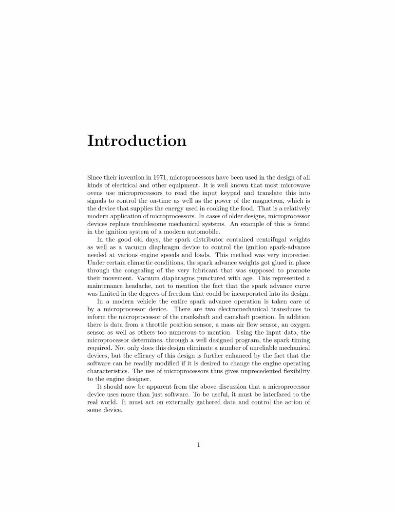
The following short subroutines can be used to communicate with the serialport.
dreg equ $10000 ; data portcsreg equ $10001 ; control status portdavbit equ 2 ; receive data available maskbfebit equ 1 ; transmit buffer empty mask;; Get a char, mask with 7fH. Char in D1.Bcharin move.b csreg,d0 ; get status
andi.b #davbit,d0 ; Mask for char input statusbeq charin ; No char, then loop backmove.b dreg,d1 ; Get the charandi.b #$7f,d1 ; Get rid of bit 7 as a precautionrts ; Char in d1.b
;; Send a char from D1.Bcharout move.b csreg,d0 ; get status
andi.b #bfebit,d0 ; Mask for buffer empty statusbeq charout ; Not empty, then loop backmove.b d1,dreg ; Send the charrts ; Done
12

The EEPROM MonitorProgram
To get this microcomputer to operate it is necessary to put a monitor programinto an EPROM or EEPROM. This design uses a 28C256 EEPROM becauseit is sufficiently large to accommodate the program that we wish to use as asystem MONITOR. This is the monitor program that has been quite thoroughlyreworked by Dave Harrison and myself. The latest version 3.00 can be found onmy website as mon300.zip SBC Monitor Program. The monitor program takesup less than 36% of the ROM, so the user has plenty of room to add additionalsoftware as desired.
The new monitor version 3.00 makes the SBC capable of executing theEASy68K TRAP #15 tasks 0-2, 4-7, 9 and 12-14. This enables the user toswitch to the windows oriented EASy68K assembler-emulator package. Thiscan be downloaded very easily. Antonakos’s latest assembler and emulator areposted on my website.
The monitor program MON300.ASM is assembled using Antonakos’s as-sembler. The program MON300.X68 can be assembled using the EASy68Kprogram. Either one of the resulatant .HEX files can then be used to burn theEEPROM as described in the next section.
Programming the EEPROM Monitor
There are PCs in room 204F, 211F as well as in room 318F, which are interfacedwith Xeltek programmer pods. To burn the EEPROM go to the \SP\BINsubdirectory and type SP<ent> then follow the steps below.
• Type <F9> to select the programming of GALs or EEPROMs, and then<esc> to get out.
• Type <F7> and use < ∗ > <ent> to select the device manufacturer, andthen <esc> to get out.
13

• Type <F8> and use < ∗ > <ent> to select the device number, and then<esc> to get out.
The proper data for the EEPROM should now appear in the right middle of thescreen. Use the FILE menu to load the HEX file that you will need to programthe chip. Use the BUFFER then EDIT feature to verify the data that has beenloaded, assuming that you have taken the trouble to memorize a few bytes ofyour code.
Go to the DEVICE screen to program the chip. It is self explanatory fromhere.
If your EEPROM fails to program under its proper brand name, then pro-gram it as a XELTEK 28C256 chip. No harm is done since all the programmingis done by toggling 5 volts on and off in a specific sequence at various pins.
14
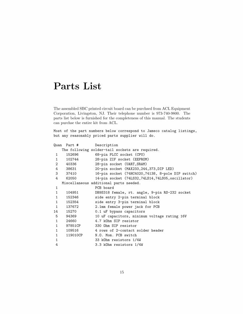
Parts List
The assembled SBC printed circuit board can be purchsed from ACL EquipmentCorporation, Livingston, NJ. Their telephone number is 973-740-9800. Theparts list below is furnished for the completeness of this manual. The studentscan purchse the entire kit from ACL.
Most of the part numbers below correspond to Jameco catalog listings,but any reasonably priced parts supplier will do.
Quan Part # DescriptionThe following solder-tail sockets are required.
1 152696 68-pin PLCC socket (CPU)1 102744 28-pin ZIF socket (EEPROM)2 40336 28-pin socket (UART,SRAM)4 38631 20-pin socket (MAX233,244,373,DIP LED)3 37410 16-pin socket (74HC4020,74138, 8-pole DIP switch)4 62050 14-pin socket (74LS32,74LS14,74LS05,oscillator)
Miscellaneous additional parts needed.1 PCB board1 104951 DB9S318 female, rt. angle, 9-pin RS-232 socket1 152346 side entry 2-pin terminal block1 152354 side entry 3-pin terminal block1 137672 2.1mm female power jack for PCB
14 15270 0.1 uF bypass capacitors5 94369 10 uF capacitors, minimum voltage rating 16V1 24660 4.7 kOhm SIP resistor1 97851CP 330 Ohm SIP resistor1 109516 4 rows of 2-contact solder header1 119010CP N.O. Mom. PCB switch1 33 kOhm resistors 1/4W4 3.3 kOhm resistors 1/4W
15
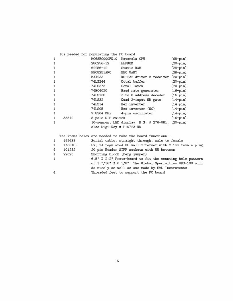
ICs needed for populating the PC board.1 MC68EC000FN10 Motorola CPU (68-pin)1 28C256-12 EEPROM (28-pin)1 62256-12 Static RAM (28-pin)1 NEC8251AFC NEC UART (28-pin)1 MAX233 RS-232 driver & receiver (20-pin)1 74LS244 Octal buffer (20-pin)1 74LS373 Octal latch (20-pin)1 74HC4020 Baud rate generator (16-pin)1 74LS138 3 to 8 address decoder (16-pin)1 74LS32 Quad 2-input OR gate (14-pin)1 74LS14 Hex inverter (14-pin)1 74LS05 Hex inverter (OC) (14-pin)1 9.8304 MHz 4-pin oscillator (14-pin)1 38842 8 pole DIP switch (16-pin)1 10-segment LED display R.S. # 276-081, (20-pin)
also Digi-Key # P10723-ND
The items below are needed to make the board functional.1 199638 Serial cable, straight through, male to female1 17301CP 5V, 1A regulated DC wall x’former with 2.1mm female plug4 101282 20 pin Header SIPP sockets with WW bottoms1 22023 Shorting block (Berg jumper)1 6.5" X 2.2" Proto-board to fit the mounting hole pattern
of 1 7/16" X 6 1/8". The Global Specialties UBS-100 willdo nicely as well as one made by E&L Instruments.
4 Threaded feet to support the PC board
16

Completing the Assemblyof the SBC
Table 1.2: Chip Socket Identification Table
Chip Chip Number74LS244 U1
68EC000 CPU U228C256 EEPROM U3
62256 RAM U474LS05 U574LS14 U674LS32 U774LS373 U874LS138 U9
8251A UART U10MAX233 serial Driver U11
74HC4020 U129.8304 MHz oscillator Y1
8 pole DIP switch SW110-segment LED display D1
To complete the assembly of the SBC the student needs to insert all the ICscarefully into their appropriate sockets, if this has not been previously done bythe supplier. Correspondence of pin 1 on the chip to that of the socket shouldbe given special attention. The EEPROM containing the MONITOR programgoes into the Zero Insertion Force (ZIF) socket. The ZIF socket was providedin case the student should want to add additional software to the EEPROM inthe future. Extra care should be exercised installing the MC68EC000 CPU asits socket is turned 90 counterclockwise. To install the chips into their correctsockets consult table 1.2.
17

It remains for the student to solder in the various headers that are neededto complete the SBC. Insert the three 20 pin header SIPP sockets making surethat the long wire-wrap pins point to the underside of the board and the socketends are face up.
Break one 20 pin header into two equal parts and insert the two resultant10 pin headers with the wire wrap pins facing down. It remains to solder all theheader pins to the SBC printed circuit board.
Caution: The long wire wrap pins are used for wire wrapping when that iscalled for. The efficacy of wire wrapping depends on having a pin with a squarecross section, with sharp 90 corners, so that the wire-wrap wire gets notchedfour times for each turn of the wire. Thus six turns produce 24 notches in thewire assuring an excellent connection. It is therefore important to make surethat the wire wrap pins not be covered with solder except near the printed cir-cuit board. Covering those pins with solder along their length will give them anundesirable round cross section. This will make reliable wire wrap connectionsimpossible.
Accordingly, when soldering in the headers, use a soldering iron with a smalltip and make sure that the solder is applied only to the bottom of each pin.Neatness is very important, not just in this case, but also in all prototypingwork in electronics.
Mount the Proto board using the holes provided and install the legs on theboard to make sure the wire wrap pins don’t get bent out of shape when theprinted circuit board is put down. The board is now ready for use. You needonly select a baud rate by installing a jumper on two pins of the 8-pin header,J5, then connect the power supply and the serial communications cable.
18

Interfacing the SBC to aPersonal Computer
The bidirectional serial interface which appears at the bottom of the microcom-puter schematic is designed to connect the microcomputer to a personal com-puter. In this kind of connection we have to make the distinction between DataTerminal Equipment (DTE) and Data Communications Equipment (DCE).
Generally, the equipment that controls the communication is consideredDTE and the PC is in that category. A MODEM or a printer with a serialinterface is considered DCE. DCE is either the intermediary or terminus for theDTE. The designation has a bearing on the configuration of the serial connectorused with each device.
Modern DTE serial ports, as found on the backs of the latest PCs, use a9-pin D-subminiature (D-sub) male connector. The DTE uses pin 3 of the 9-pinconnector for sending data, pin 2 for receiving data and pin 5 for ground.
The SBC is considered DCE. A 3-wire flexible cable, about 4 feet in length,should be used to connect the RS-232 serial signals coming from the MAX233chip to a 9-pin D-sub female connector. This 9-pin female connector should havepin 3 connected to the RS-232 input on the MAX233 chip, and pin 2 connectedto the RS-232 output from that same chip. Pin 5 is connected to ground.
The baud rate can be set at something fast, such as 38,400 baud, and thePC communication software should be set to match that rate. If all is connectedcorrectly then communication should be established immediately.
The most straightforward program to use for communicating with the SBCis HyperTerminal. But it leaves a great deal to be desired, because it is slow intransferring ASCII HEX files from the PC to the SBC. A better choice is thepublic domain communication program TTermPro (a.k.a. TeraTermPro). It hasno shortcomings, but should it prove troublesome in ASCII HEX file transferthen just go to SETUP, then SERIAL PORT and specify a 30msec/line timedelay. It won’t affect the transfer rate noticeably, but will make the file transferreliable.
19

Future Uses of the SBC
The Proto board was furnished to facilitate the interfacing experiments in theMicroprocessor laboratory. But the SBC can be used for projects which needthe decision making power of a microprocessor.
If you decide to use the SBC as part of your senior project then you sim-ply remove the Proto board to gain access to a fairly big wire-wrap area. Wirewrapping is more reliable than using a Proto board for large interfacing projectsand you can also get more chips into a given area. Less than 36% of the EEP-ROM is filled with the MONITOR program. There is plenty of memory leftfor adding software that is needed to operate devices that are interfaced to theSBC.
You should keep the above options in mind before you consider getting ridof your SBC.
20

The Experiments
Experiment 1 - Acquiring and Completing theSBC
Once the preceding tutorial material has been read and understood, the studentsshould proceed with the procurement and final assembly of the microprocessor.As described above, this involves the programming of the EEPROM, the instal-lation of the chips, the soldering-in of the wire-wrap headers, the installation ofthe Proto board and the installation of the feet to support the board. This canall be accomplished before the second meeting of the class.
During each course meeting the instructor should check each students’ progress.This is to make sure that procrastinators do not get rewarded with high grades.The idea is to maintain momentum from the first day on. Failure to demonstratecompetence in the course through the demonstration of a substantial numberof competently completed experiments should result in course failure.
21

Experiment 2 - Developing Software for the SBC
Although you may have written much of the software that follows in the micro-processor lecture course, you now have the opportunity to test the software inits native environment. Previously you could only test software using a cross-emulator on a PC. It is therefore worthwhile to perform the experiments belowin order to acquire greater familiarity with the MC68EC000 microprocessor.
Finding the Position of a Letter in a String
The students should use the Antonakos’s cross-assembler to write a program forfinding the position of the letter ’x’ in any one of the following strings:
1. I have never seen a better experiment.
2. This is an overly short and dull experiment.
3. This is a fairly simple but exciting experiment.
4. This is an interesting though not long experiment.
5. Hmm, this isn’t as dull as all that, as experiments go.
This short program can then be downloaded into the microprocessor and tested.The string should be stored in the RAM that immediately follows the re-
quired program. This is done using the DC.B directive. The position of theletter ’x’ in the string should be displayed on the LEDs of the parallel outputport.
Now modify the string in the SBC, by using the monitor’s EDIT feature,to replace the ’x’ with another character. When the string contains no ’x’ then0FFH should be displayed on the LEDs of the parallel output port.
Moving a string in RAM
Write and debug a program for moving a string of bytes of arbitrary lengthfrom one memory location to another. The A0 register is initialized to point tothe beginning of the data source, the A1 register is initialized to point to thebeginning of the data destination, and the D1 register is initialized to containthe count. This program will pick up the data one byte at a time and depositit one byte at a time. The transfer is complete when the (16 bit) D1 register isdown to zero. The program should first fill the destination area with 0FFHs sothat the success of the move will be perfectly clear.
Even though your string may be quite short, your software mustbe prepared to transfer up to 64 kbytes of data.
22

Addition of Numbers with Keyboard Input
An available monitor task can be used to obtain ASCII characters in D1.Bfrom the PC keyboard. Numerical characters (digits), ’0’ to ’9’, should beconverted to BCD by stripping off the 30 H. Suppose there are 4 BCD digits,e.g. d4, d3, d2, d1.These can be converted to a HEX number, useful for furtherarithmetical use, by utilizing the looping routine:
HEX number = [(d4 ∗ 10 + d3) ∗ 10 + d2] ∗ 10 + d1
If, for example, the decimal number typed-in is 8102, then the resultant HEXnumber should be 1FA6H
Using the above information, write a subroutine which will accept a decimalnumber from the keyboard, maximum length of 4 digits, and convert it to aHEX number in a D-register.
Another available monitor task can be used to send ASCII characters inD1.B to the screen. To display the decimal equivalent of a HEX number onthe screen, the decimal digits contained in the HEX number have to be madeavailable. This is done by continuously dividing the number by 10D. Take, forexample, the number 23AF H. We divide it by 10 D to obtain 23AF H / 10D =391H, with a remainder of 5. The 5 is the least significant decimal digit of thisnumber. When this is ORed with 30 H it becomes the ASCII 35 H. The processis repeated so that 391H / 10D = 5BH with a remainder of 3, and so on. Theresult for the above number should be ’9135’ in ASCII.
Using the above information, write a subroutine which will take a HEX wordin a D-register and print the decimal equivalent on the screen.
When the above subroutines are finally available write a program that willperform the addition of two 4 digit numbers obtained from the keyboard anddisplay the result on the screen. For example if you type: 4562 + 9371 = thenthe program should skip a line and type out on the screen: 4562+9371 = 13933.
Prelab Assignment
Prepare the commented assembly language program well before the experimentis performed, and bring the software to class on a diskette.
23

A B
F
TEST
HLA
Green Amber Green
Flashing Amber Flashing Red
Red
C
ACK E
HLA
Flashing Amber
Flashing Red
LLA
D
HLA
. TEST LLA LLA HLA . LLA HLA .
ACK LLA HLA . .
Figure 1.2: State diagram of the annunciator circuit.
Experiment 3 — An Event Driven AnnunciatorSystem
In an event driven sequential device, the next state is determined by the presentstate of the device as well as by the state of the inputs. A sequential circuithas to have memory devices, such as D or J-K flip-flops as well as supportingcombinatorial circuitry.
The difficulty with the design described above is that once it is implementedit is difficult to modify. If a change in the sequence is desired then a newprinted circuit board layout may be necessary and perhaps even the additionof more ICs. This difficulty is circumvented by using a microprocessor or amicrocontroller at the heart of the design. A change in the design might merelyinvolve a reprogramming of the ROM that controls the device.
The event driven sequential circuit will be implemented in this experimentis not clock driven. It is consequently called a free running circuit because theoutput responds to an input change and not to a clock. It is clearly the inputchanges which drive the circuit, so the circuit is called event driven. Othernames commonly used are nonpulse circuits or asynchronous circuits.
The state diagram for the sequential circuit that we wish to design is shownin figure 1.2. It is a two alarm system which might be used in a factory tosignal that various levels of faults are occurring on the production line. Oneapplication may be in process control, where the fault could indicate an elevatedpressure. A flashing amber light would indicate the first stage of pressure change,a potential hazard. A large change in the system, shown by a flashing red lightwould indicate an emergency condition.
The operation of the circuit is best described by the state diagram of figure1.2. The circuit operates in the following manner:
24

1. With no fault-signal present the system is stable, it is in state B, and theGREEN light is on.
2. When the signal LLA is present, indicating a minor fault, the state changesto C, a FLASHING-AMBER light comes on and the GREEN light goesoff. If the fault disappears (LLA), the annunciator returns directly to thenormal GREEN state.
3. When the system is in the minor-fault (FLASHING-AMBER) state, anoperator can intervene to clear the minor fault by pushing the acknowledgebutton which contains a momentary contact switch. The presence of theACK signal for a mere fraction of a second changes the system to thesteady-AMBER state, telling supervisory personnel that someone is tryingto clear the fault. If the minor fault is cleared (LLA) then the annunciatorreturns to the normal (GREEN) state after 2 clock pulses.
4. If the system is in the AMBER or FLASHING-AMBER state and themajor fault signal (HLA) is received, the system signals a major faultby changing to the FLASHING-RED state. Even if this signal is onlymomentary, this condition will be maintained indefinitely. The presenceof the ACK signal for a mere fraction of a second causes a transitionto the steady-RED state, telling supervisory personnel that someone istrying to clear the major fault. If the major fault is cleared (HLA), theannunciator starts on its path to the normal state and finally attains it ifthere is no low level alarm (LLA).
5. A test pushbutton is included to check the condition of all the lights. OnTEST , the GREEN, FLASHING-AMBER and FLASHING-RED lightsshould be on. This is the A state.
On the prototyping board interface 3 LEDs with the parallel output port.Keep in mind that LEDs have a constant voltage drop across them of approx-imately 1.6 volts. A resistor of approximately 330 Ω must be wired in serieswith each LED to limit its current to 10 mA. The existing DIP switch can beused for the various input signals. Labeling the switches and LEDs with a smallamount of masking tape will go a long way to keeping the final presentationcomprehensible.
Write the software required to implement the annunciator circuit. Demon-strate the working model to the instructor.
25

Prelab Assignment
1. Procure some LEDs, of different colors if possible, as well as some 330Ωresistors.
2. On a diskette, prepare the commented assembly language program to drivethe LEDs according to the specifications shown in figure 1.2.
26

Experiment 4 — Testing and Simulating SomeICs
The SBC as an IC Test Jig
The student should obtain three (3) common combinatorial chips, such as the7400, 7408, 7432 or whatever. The microprocessor should be used to output avoltage test pattern to the chip using the output port and to read back the chipoutput using the input port. Pass or fail should be signaled on completion ofthe test by putting a 0 or 0FFH in D0.B.
The above should be demonstrated for each of the combinatorial chips. Aworking chip can be made to look defective if one of its input pins is pulled fromthe socket and left hanging in mid-air.
The SBC Used to Simulate D and J-K flip-flops
The SBC will be used to simulate a D type flip-flop. The inputs are D andCLOCK and the outputs are Q and Q. The input should be read when CLOCKis high and should be transferred to the output when the CLOCK signal dropslow. The software should be written to guarantee that no false triggering cantake place due to a sudden noise spike.
Repeat the above experiment for a J-K type flip flop.
Prelab Assignment
1. Procure the chips needed for this experiment.
2. On a diskette, prepare the commented assembly language program to ac-complish the tasks required.
27
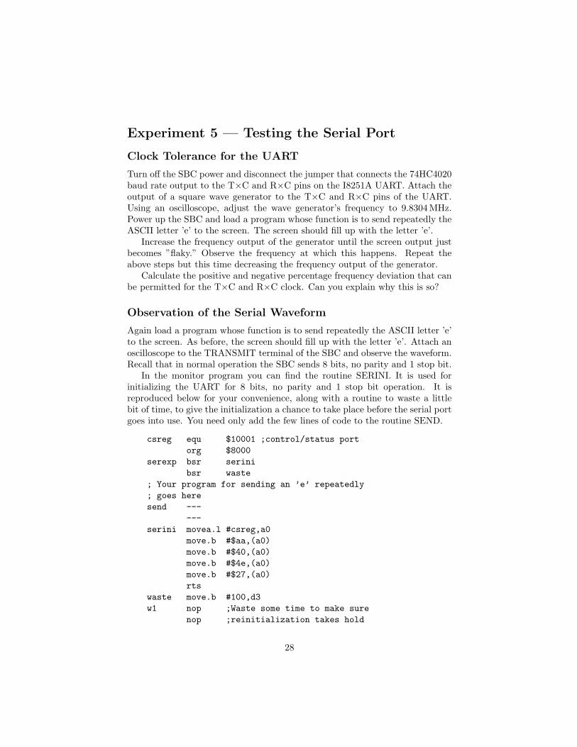
Experiment 5 — Testing the Serial Port
Clock Tolerance for the UART
Turn off the SBC power and disconnect the jumper that connects the 74HC4020baud rate output to the T×C and R×C pins on the I8251A UART. Attach theoutput of a square wave generator to the T×C and R×C pins of the UART.Using an oscilloscope, adjust the wave generator’s frequency to 9.8304 MHz.Power up the SBC and load a program whose function is to send repeatedly theASCII letter ’e’ to the screen. The screen should fill up with the letter ’e’.
Increase the frequency output of the generator until the screen output justbecomes ”flaky.” Observe the frequency at which this happens. Repeat theabove steps but this time decreasing the frequency output of the generator.
Calculate the positive and negative percentage frequency deviation that canbe permitted for the T×C and R×C clock. Can you explain why this is so?
Observation of the Serial Waveform
Again load a program whose function is to send repeatedly the ASCII letter ’e’to the screen. As before, the screen should fill up with the letter ’e’. Attach anoscilloscope to the TRANSMIT terminal of the SBC and observe the waveform.Recall that in normal operation the SBC sends 8 bits, no parity and 1 stop bit.
In the monitor program you can find the routine SERINI. It is used forinitializing the UART for 8 bits, no parity and 1 stop bit operation. It isreproduced below for your convenience, along with a routine to waste a littlebit of time, to give the initialization a chance to take place before the serial portgoes into use. You need only add the few lines of code to the routine SEND.
csreg equ $10001 ;control/status portorg $8000
serexp bsr serinibsr waste
; Your program for sending an ’e’ repeatedly; goes heresend ---
---serini movea.l #csreg,a0
move.b #$aa,(a0)move.b #$40,(a0)move.b #$4e,(a0)move.b #$27,(a0)rts
waste move.b #100,d3w1 nop ;Waste some time to make sure
nop ;reinitialization takes hold
28
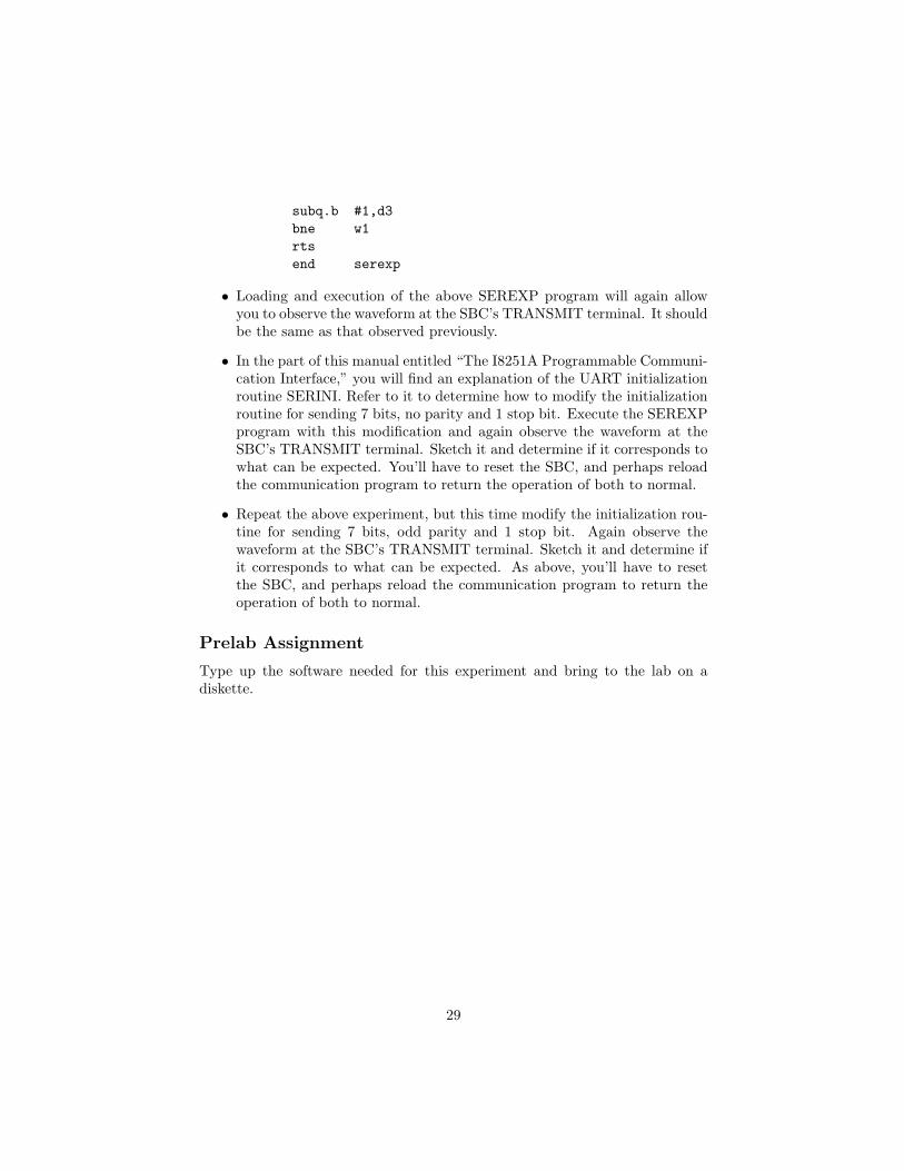
subq.b #1,d3bne w1rtsend serexp
• Loading and execution of the above SEREXP program will again allowyou to observe the waveform at the SBC’s TRANSMIT terminal. It shouldbe the same as that observed previously.
• In the part of this manual entitled “The I8251A Programmable Communi-cation Interface,” you will find an explanation of the UART initializationroutine SERINI. Refer to it to determine how to modify the initializationroutine for sending 7 bits, no parity and 1 stop bit. Execute the SEREXPprogram with this modification and again observe the waveform at theSBC’s TRANSMIT terminal. Sketch it and determine if it corresponds towhat can be expected. You’ll have to reset the SBC, and perhaps reloadthe communication program to return the operation of both to normal.
• Repeat the above experiment, but this time modify the initialization rou-tine for sending 7 bits, odd parity and 1 stop bit. Again observe thewaveform at the SBC’s TRANSMIT terminal. Sketch it and determine ifit corresponds to what can be expected. As above, you’ll have to resetthe SBC, and perhaps reload the communication program to return theoperation of both to normal.
Prelab Assignment
Type up the software needed for this experiment and bring to the lab on adiskette.
29

Experiment 6 — DAC Interface with the SBC
Objectives
This experiment is used to familiarize students with interfacing computers to theanalog world. This is necessary because in the real world there are multitudesof analog devices which need to be interfaced to digital equipment. To interfacecomputers and digital devices to the analog world we commonly use A/D (analogto digital) and D/A (digital to analog) converters. The A/D converter takes ananalog signal and converts it to a digital value. The output is the ratio of theinput voltage to the reference voltage of the A/D converter. The D/A converterdoes the opposite. It takes the digital value and generates an analog voltagewhich is proportional to a reference voltage.
COMP
+2.5V
1.25k
D0 D1
D3 D2
D4 D5 D6 D7 A1
A3 A2
A4 A5 A6 A7 A8
(MSB)
(LSB)
GND V EE
V CC
V ref (+)
V ref (-)
1.25k
+15V
-15V
2.5k
OUT
R ref
R o 5k
15pF
+ AD741
+15V
-15V
V out
P output port R BP
R a
DA
C08
08
Figure 1.3: The DAC connection to the microprocessor board.RBP is used only in the bipolar configuration.
In this experiment a DAC0808 8-bit digital to analog converter is interfacedto the microprocessor parallel I/O output port as shown in figure 1.3. This setupwill then be used for the generation of square, sine and triangular waveforms.
The D/A converter used in this experiment is the DAC0808 available fromNational Semiconductor. The specification sheets can be obtained from theNational Semiconductor Linear Data Book available in the stockroom.
30

Prelab Assignments
1. Prepare commented assembly language programs to generate the wave-forms in the following section. Prepare flow charts for these programs.Do not replicate common portions of the code or flow charts.
2. Compute the current flow out of the DAC of figure 1.3 when it sees thefollowing data bytes:
(a) 30H
(b) 0A1H
(c) 0FAH
Assume that the reference voltage Vref = 5.0 V and that Rref = 5KΩ.
Lab assignments
Connect the DAC and associated components to the output port of the micro-processor. Write programs to output a binary sequence so as to generate:
1. A Square Wave (both unipolar and bipolar)
2. A Sawtooth Wave (both unipolar and bipolar)
3. A Sine Wave (bipolar only)
The waves should be periodic, with a period controllable by a scale storedin a specific RAM address. Select a reasonable range of frequencies, takinginto account the dynamic properties of the DAC and of your microcomputer.Display the output waveforms on an oscilloscope.
31

Experiment 7 — The Logic Analyzer
Objectives
The objective of this experiment is to familiarize students with the use of alogic analyzer for trouble shooting digital devices. This is to be accomplishedthrough an examination of the bus signals of the SBC.
Introduction
The instrument that is used a great deal in the troubleshooting of electricalcircuitry is the oscilloscope. It permits the viewing of waveforms in great detail,determining rise-times and fall-times of pulse waveforms and the viewing of anykind of analog signals. Oscilloscopes are capable of displaying two traces atonce, and this is not too useful in studying the behavior of digital circuits. Thisis where the logic analyzer becomes very useful.
This piece of test equipment can display multiple signals at once, but it mustbe understood that it does not give a detailed presentation of the signal. Whenyou read the logic analyzer manual you discover its limitations. It squares upall waveforms that it is examining. It looks for transitions of digital states fromlow to high and conversely. Thus, a sinewave will look like a square wave on alogic analyzer. So it should not be used for the study of analog waveforms. Itsstrong point is its ability to display multiple waveforms when troubleshootingdigital circuitry.
The Experiment
Obtain one of the four logic analyzers from the stockroom. You’ll find that ithas 4 pods with 16 leads each. The SBC signals that the analyzer needs to seeare brought out to the single row 20-pin headers that you installed earlier on theboard. Hook-up leads to the clock signal CLK, the 8 data bus signals D7–D0,the 15 address bus signals A14–A0, RD, WD, and AS.
An examination of the monitor program of the SBC will reveal that it isusually busy getting a keyboard command. The GETLIN routine is responsiblefor this. It loops to the label GETCHAR within that routine. Setting theanalyzer to trigger on the HEX address of GETCHAR will cause it to capturethe bus signals of interest.
• Compare the waveforms obtained with the timing waveforms for the syn-chronous read appearing in the Supplementary Notes for the prerequisitemicrprocessor lecture course.
• Have the logic analyzer show the data obtained in HEX number form. Seeif it corresponds to the listing of the GETCHAR routine.
32

Write a short program with an endless loop for writing a word of some datacontinuously to address $8100. Set the analyzer to trigger at the start of thisloop.
• Compare the waveforms obtained with the timing waveforms for the syn-chronous write appearing in the Supplementary Notes for the prerequi-site micrprocessor lecture course.
• Have the logic analyzer show the data obtained in HEX number form. Seeif it corresponds to the listing of the GETCHAR routine.
• Since the CPU is operating in 8-bit mode, writing a word to memoryshould require two physical memory write accesses. See if this is indeedthe case.
33

Dr.
Sol
Ros
enst
ark
EC
E D
epar
tmen
t N
JIT
N
ewar
k, N
J Ju
ne 1
0, 1
997
3 4 P
A0
PA
1 P
A2
PA
3 P
A4
PA
5 P
A6
PA
7
40
1 2 37
38
39
PB
0 P
B1
PB
2 P
B3
PB
4 P
B5
PB
6 P
B7
15
14
PC
0 P
C1
PC
2 P
C3
PC
4 P
C5
PC
6 P
C7
13
17
16
10
11
12
19
18
22
21
20
25
24
23
8255A PPI
RD
C
S
WR
RE
SE
T
34
30
32
33
27
28
29
31
D0
D1
D2
D3
D4
D5
D6
D7
A1
A0
35
6 5 36
8 9
GN
D
V cc
26
7 Fig
. A.1
- 8
255
pino
ut
8255A
PA
7 -
PA
0
PC
3 -
PC
0
PB
7 -
PB
0
CW
= 1
0010
000
Fig
. A.2
- T
wo
exam
ples
of m
ode
0
8 8 4 4
PC
7 -
PC
4
8255A
PA
7 -
PA
0
PC
3 -
PC
0
PB
7 -
PB
0
CW
= 1
0011
010
8 8 4 4
PC
7 -
PC
4
PC
7
PC
6
PC
3
8
PC
4,5
OB
F A
INT
R A
AC
K A
PC
1
PC
2
PC
0
8
CW
= 1
XX
XX
10X
OB
F B
INT
R B
AC
K B
WR
WR
Fig
. A.4
- T
wo
exam
ples
of
mod
e 1
OU
TP
UT
F
ig. A
.3 -
Tw
o ex
ampl
es o
f m
ode
1 IN
PU
T
PC
2
PC
1
PC
0
8
CW
= 1
XX
XX
11X
ST
B B
IBF
B
INT
R B
PC
4
PC
5
PC
3
8
ST
B A
IBF
A
INT
R A
RD
PC
6,7
RD
2
2
PB
7 -
PB
0
PA
7 -
PA
0 P
A7
- P
A0
PB
7 -
PB
0
CW
= 1
010Y
XX
X
CW
= 1
011Y
XX
X 1
= IN
PU
T
PO
RT
C
0 =
OU
TP
UT
INT
E B
INT
E A
INT
E A
INT
E B
PC
4
PC
5
PC
6
PC
7
PC
3
PA
7 -
PA
0 8
INT
R A
ST
B A
IBF
A
OB
F A
AC
K A
WR
RD
3 P
C2-
0
Fig
. A.6
- M
ode
2
INT
E 1
INT
E A
IBF
A IN
TR
A I/O
I/O
IB
F B
INT
E B
INT
R B
D 0
D 1
D 5
D 7
D 6
D 2
D 4
D 3
INP
UT
CO
NF
IGU
RA
TIO
N
OU
TP
UT
CO
NF
IGU
RA
TIO
N
GR
OU
P A
G
RO
UP
B
INT
E A
OB
F A
INT
R A
I/O I
/O
INT
E B
INT
R B
D 0
D 1
D 5
D 7
D 6
D 2
D 4
D 3
OB
F B
Fig
. A.5
- M
ode
1 S
tatu
s W
ord
For
mat
GR
OU
P A
G
RO
UP
B
INT
E 1
OB
F A
INT
R A
D 0
D 1
D 5
D 7
D 6
D 2
D 4
D 3
Fig
. A.7
- M
ode
2 S
tatu
s W
ord
For
mat
GR
OU
P A
G
RO
UP
B
IBF
A IN
TE
2
1 =
INP
UT
P
OR
T C
0
= O
UT
PU
T
INT
E 2
34
Appendix A — OptionalParallel Port Expansion
Introduction
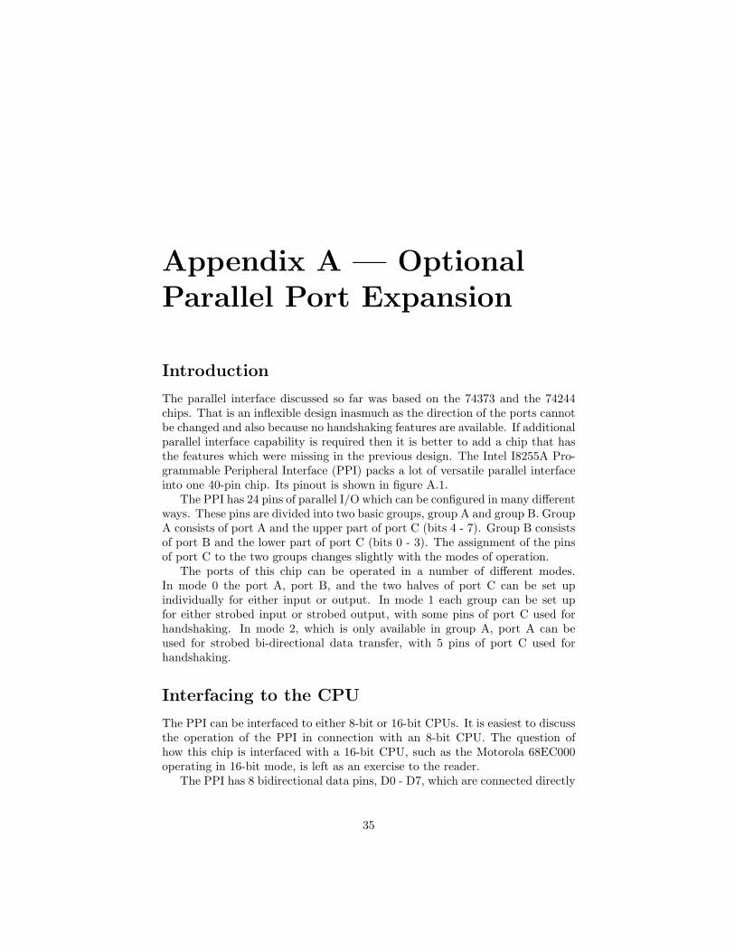
The parallel interface discussed so far was based on the 74373 and the 74244chips. That is an inflexible design inasmuch as the direction of the ports cannotbe changed and also because no handshaking features are available. If additionalparallel interface capability is required then it is better to add a chip that hasthe features which were missing in the previous design. The Intel I8255A Pro-grammable Peripheral Interface (PPI) packs a lot of versatile parallel interfaceinto one 40-pin chip. Its pinout is shown in figure A.1.
The PPI has 24 pins of parallel I/O which can be configured in many differentways. These pins are divided into two basic groups, group A and group B. GroupA consists of port A and the upper part of port C (bits 4 - 7). Group B consistsof port B and the lower part of port C (bits 0 - 3). The assignment of the pinsof port C to the two groups changes slightly with the modes of operation.
The ports of this chip can be operated in a number of different modes.In mode 0 the port A, port B, and the two halves of port C can be set upindividually for either input or output. In mode 1 each group can be set upfor either strobed input or strobed output, with some pins of port C used forhandshaking. In mode 2, which is only available in group A, port A can beused for strobed bi-directional data transfer, with 5 pins of port C used forhandshaking.
Interfacing to the CPU
The PPI can be interfaced to either 8-bit or 16-bit CPUs. It is easiest to discussthe operation of the PPI in connection with an 8-bit CPU. The question ofhow this chip is interfaced with a 16-bit CPU, such as the Motorola 68EC000operating in 16-bit mode, is left as an exercise to the reader.
The PPI has 8 bidirectional data pins, D0 - D7, which are connected directly
35

Table 1.3: Decoding Table for the PPI
Register Pin Designation AddressPort A PA0 – PA7 8000HPort B PB0 – PB7 8001HPort C PC0 – PC7 8002H
Control Word Register (CWR) 8003H
to the CPU data bus. This chip has separate RD and WR pins, which in ourmicroprocessor project would be interfaced with the two signals with that samedesignation, derived from the 74LS32 OR-gates. The RESET pin would be tiedto the RESET signal used for the I8251A serial interface chip.
The chip select signal CS can be connected to one of the 74LS138 decoderoutputs. If it were tied to the output O4 then it would be decoded starting at8000H. The device has two pins marked A0 and A1. With our CPU these pinscan be connected to the correspondingly marked CPU address bus pins. ThePPI is then addressed according to the decoding table 1.3.
Selecting the Operating Modes of the PPI
As mentioned in the introduction, the ports of the PPI are divided into twogroups. Port A and the upper part of port C (bits 4 - 7) belong to groupA. Port B and the lower part of port C (bits 0 - 3) belong to group B. Theassociation of the parts of port C to the two groups is rather loose and bit 3 isshifted to group A when that group is used in mode 1 or mode 2.
Assigning Modes and Port Directions
The device can be operated in three modes. The modes of operation are se-lectable by writing a control byte to the CWR register. The bits of the controlbyte have a specific grouping. The control byte bits, designated
D7, D6, D5, D4, D3, D2, D1, D0
are used to select the following modes of operation:
• D7 is the mode set flag. It must be 1 to activate mode setting.
• D6, D5 are used to select the mode of operation of group A. They areused as follows:
1. D6, D5 =00 selects mode 0.2. D6, D5 =01 selects mode 1.3. D6, D5 =1X selects mode 2.
• D4 determines the direction of port A. Input = 1 and Output = 0.
36

• D3 determines the direction of the upper half of port C. Input = 1 andOutput= 0.
• D2 is used to select the mode of operation of group B. D2= 0 selects mode0 and D2 =1 selects mode 1. This group has no mode 1.
• D1 determines the direction of port B. Input = 1 and Output = 0.
• D0 determines the direction of the lower half of port C. Input = 1 andOutput= 0.
Individual Bit Set/Reset Capability of Port C
In setting the mode of operation of the PPI we needed to write to the CWRusing D7 =1. Writing to the CWR with D7 = 0 can be used to set or resetspecific bits of port C, one bit at a time. This assumes that port C is beingused for output and not for input. If a group is in mode 0 then its portionof port C can be written to directly. In the two other modes the only way tochange the output bits of port C is to use the bit set/reset method mentionedabove.
To use the port C individual bit set/reset method, the control byte bits,designated
D7, D6, D5, D4, D3, D2, D1, D0
are used as follows:
• We need D7= 0 for port C bit setting to take place.
• D6, D5 and D4 are “don’t cares.”
• D3, D2 and D1 determine which bit of port C will be affected, with 000designating bit 0, 001 designating bit 1 and so on.
• The value of D0 determines the value that the bit will take.
It should be noted that when ports are used for output, the last value writtento them can be read back. This does not apply to the CWR.
The Operating Modes of the PPI
In the previous section it was explained how to obtain the various modes ofoperation. Now we need to become familiar with how those modes affect theoperation of the ports of the PPI. But before we proceed, a few importantobservations are in order.
If any group is programmed in mode 0 for output, then the data can besent to those pins by simply writing to port C. This is not true if a group isprogrammed in any mode other than mode 0. If it is desired to write any data
37

to port C, when the group to which that port belongs is in mode 1 or 2, thenthis must be done on a bit by bit basis using the bit set/reset method. Hence ifpins PC6,7 are used for output, in one of the two higher modes, then the datamust be sent to them using the bit set/reset method.
In any mode, if any pins of port C are used for input then the data can beobtained by simply reading port C.
Mode 0 — Simple Input/Output
In mode 0 the ports are used for input or output without any handshaking. Asan example, writing the control word CW =10010000 to the CWR will causemode setting to take place, and configure group A for input in mode 0. Theupper part of port C will be configured for output. This CW will also configuregroup B for output in mode 0. The lower part of port C will be configured foroutput. This port configuration is demonstrated in figure A.2.
As another example, writing the control word CW= 10011010 to the CWRwill configure group A for input in mode 0. The upper part of port C will alsobe configured for input. Group B will also be configured for input in mode 0.The lower part of port C will be configured for output. This port configurationis also demonstrated in figure A.2.
Mode 1 — Strobed Unidirectional Data Transfer
In mode 1 the ports are used for input or output with handshaking. If onegroup is used in mode 1, the other group can be used in any available mode.In mode 1 the five pins PC3-7 are assigned to group A. This leaves PC0-2 ofport C assigned to group B. In figure A.3 we see how to configure group A andgroup B in mode 1 for input. In figure A.4 we see how to configure group Aand group B in mode 1 for output. It is important to note that if group A isused on mode 1, then two pins of this group are left over for simple I/O. Whengroup B is used in mode 1, however, then the three pins of lower port C are allassigned to handshaking duty. This is clearly demonstrated in figures A.3 andA.4.
The handshaking for the upper diagrams of figure A.3 and figure A.4 willbe explained in detail. The other two cases can then be understood withoutfurther explanation.
When group A is used for input in mode 1, as is the case for the upperdiagram in figure A.3, then the external device checks the “Input Buffer Full”pin, IBFA. If this pin is low, indicating that the input buffer is empty, then theexternal device puts a byte on pins PA7-PA0 and strobes it in by momentarilypulling down the STBA pin. The IBFA goes high and stays in that state untilthe data is read by the CPU. If the INTE A bit is set then the INTRA pin alsogoes high. This can be used to interrupt the CPU and to inform it to call an
38

interrupt routine to read port A. The INTRA stays high until the data is readby the CPU at which point the input cycle can be repeated.
The CPU can keep itself informed of the progress of the data transfer byreading port C. The bit patterns for INPUT and OUTPUT are shown in figureA.5. If the IBF bit is set then the CPU knows that a new byte is waiting in theinput buffer and that it can be read.
When group A is used for output in mode 1, as is the case for the upperdiagram in figure A.4, the CPU reads the status word in port C and determinesif the “Output Buffer Full” OBFA bit is inactive high. If that is the case then itcan write a byte to port A. This causes the OBFA status bit to become activelow signaling the CPU that the port A buffer is full. In addition the OBFA pinon the PPI goes low.
The external device checks the OBFA pin. If this pin is low, indicating thatthe output buffer is full, then the external device reads the data and momen-tarily strobes low the ACKA pin. In response to this the OBFA pin goes highinforming the peripheral that there is no new data for it to read. The corre-sponding OBFA status bit also goes high informing the CPU that the data hasbeen read by the peripheral. If the INTE A bit is set then the INTRA pin alsogoes high. This can be used to interrupt the CPU and to inform it to call aninterrupt routine to send a new byte to port A.
In figures A.3 and A.4 the INTE flip-flops are shown connected with dashedlines to the bit in port C that controls them. Thus, for setting INTE A, for thecase shown in the upper diagram of figure A.3, it is necessary to use the bit setfeature of the CWR to write a 1 to PC4. Reading of port C produces the statusinformation shown in figure A.5 and the status of the INTE bits can be verifiedthis way.
Mode 2 — Strobed Bidirectional Data Transfer
Mode 2 can be used only for group A for bidirectional data transfer with fullhandshaking. Group B can be used in mode 0 or mode 1 at the same time.The utilization of the pins is demonstrated in figure A.6. Careful examinationof this figure reveals that it is composite of the upper two diagrams of figuresA.3 and A.4. The handshaking which was explained for mode 1 applies here aswell. The only difference is that there are two INTE flip-flops for the INTRApin. One controls the interrupt enabling for output, the other for input.
As in the case of mode 1, reading of port C produces the status informationshown in figure A.7. If interrupts are used for both input and output, the factthat there is only one INTRA pin means that the CPU must consult the statusword to determine whether an input or output should be performed.
39