Embed Size (px)
Citation preview


EXPERIMENTAL INVESTIGATIONS OF PSEUDOSPARK DISCHARGE AND
PSEUDOSPARK PRODUCED INTENSE ELECTRON BEAMS
by
JING HU
A DISSERTATION
Presented to the Faculty of the Graduate School of the
MISSOURI UNIVERSITY OF SCIENCE AND TECHNOLOGY
In Partial Fulfillment of the Requirements for the Degree
DOCTOR OF PHILOSOPHY
in
AEROSPACE ENGINEERING
2012
Approved by
Joshua L. Rovey, Advisor
Kakkattukuzhy M. Isaac,
David W. Riggins,
Scott M. Kovaleski
Carlos H. Castano

2012
Jing Hu
All Rights Reserved

iii
PUBLICATION DISSERTATION OPTION
This dissertation has been prepared in three papers for publication in the style
used by Missouri University of Science and Technology. Three journal articles which
have been published or are under review are presented in this dissertation on various
topics of the pseudospark discharge. Paper 1 “Experimental investigation of formation
time in single-gap pseudospark discharge” has been published in Journal of Physics D:
Applied Physics, 45(2012) 465023. Paper 2 “Faraday cup with nanosecond response and
adjustable impedance for fast electron beam characterization” has been published in
Review of Scientific Instruments, 82 (7) 073504. Paper 3 “Experiment investigation of
time-resolved electron beam energy distributions generated in a transient hollow cathode
discharge” has been submitted to Journal of Applied Physics and is currently under
review.

iv
ABSTRACT
This dissertation focuses on the pseudospark discharge, a pulsed discharge
discovered for the first time in 1970’s. This dissertation is prepared as three journal
articles in the style used by Missouri University of Science and Technology. A high
voltage pseudospark discharge experiment setup, and discharge and electron beam
diagnostic system are constructed and presented in this work. Three journal articles
which have been published or are under review are presented in this dissertation on
various topics of the pseudospark discharge.
Paper 1 “Experimental investigation of formation time in single-gap pseudospark
discharge” is focused on experimental investigations of the time-dependent
characteristics of single gap pseudospark discharge device in order to understand the
initiation of the discharge current increase and build-up of a highly conductive channel
during the high current main discharge phase, which is important for pseudospark
performance as a switching device. Paper 2 “Faraday cup with nanosecond response and
adjustable impedance for fast electron beam characterization” presents a specifically
designed Faraday cup diagnostic with fast response time of 8.6 ns that is used to
determine the time-resolved electron beam energy distribution function by the self-biased
method. Paper 3 “Experimental investigation of time-resolved electron beam energy
distributions generated in a transient hollow cathode discharge” describes a more
accurate method to determine time-resolved electron energy spectrum of pseudospark
electron beams using a retarding potential energy analyzer (RPEA) specifically designed
for pulsed electron beams within the pressure range of tens of mTorr. The time-dependent
electron beam energy spectrum generated by multi-gap pseudospark discharge, and the
dependence of generated electron energy on external parameters are presented in this
work. Experimental investigations under applied potential of 5 kV, 10 kV, 15 kV and 20
kV were carried out and the time-resolved electron energy distributions are constructed.
Additionally, the energy efficiency of pseudospark produced electrons is also calculated
for energy cost evaluation and compared with the requirement of intense electron beam
applications in this work.

v
ACKNOWLEDGMENTS
I wish to express my most sincere gratitude to my advisor Dr. Joshua Rovey.
Without his patience, insightful guidance and encouragement, this work would not be
possible. I must acknowledge my appreciation to all the members of my dissertation
committee, Dr. Kakkattukuzhy Isaac, Dr. David Riggins, Dr. Scott Kovaleski, and Dr.
Carlos Castano for all the interesting discussions on pulse power and charge particle
physics issues and inspiring supervision of this work. I would also like to express my
thanks to all my colleagues in the Aerospace Plasma Laboratory at Missouri S&T for
their encouragement, assistance, and enlightening conversations.
On a personal level, I must express my gratitude to my boyfriend Keyou for his
endless patience and encouragement. I could never complete my research work without
his support. I would also like to express my appreciation to my parents Qingli and
Xiurong for their support.

vi
TABLE OF CONTENTS
Page
PUBLICATION DISSERTATION OPTION ................................................................... iii
ABSTRACT ....................................................................................................................... iv
ACKNOWLEDGMENTS .................................................................................................. v
LIST OF ILLUSTRATIONS .............................................................................................. x
LIST OF TABLES ........................................................................................................... xiv
SECTION
1. INTRODUCTION .................................................................................................... 1
1.1 MECHANISM AND CONFIGURATION OF PSEUDOSPARK
DISCHARGE ......................................................................................................1
1.1.1 Predischarge ................................................................................................ 3
1.1.2 Hollow Cathode Discharge ......................................................................... 3
1.1.3 High Current Main Discharge ..................................................................... 4
1.1.4 Decay of Plasma.......................................................................................... 4
1.2 APPLICATIONS OF PSEUDOSPARK DISCHARGE .....................................5
1.2.1 Fast Gas Switches ....................................................................................... 5
1.2.2 Intense Electron Beam Source .................................................................... 6
1.2.3 Specific Applications of Intense Electrons Beams in Aerospace Area ...... 6
1.3 CURRENT CHALLENGES AND LIMITATIONS ...........................................9
1.3.1 Fundamental Mechanisms in Pseudospark Discharge .............................. 10
1.3.2 Diagnostic of Pulsed Fast Electron Beams ............................................... 10
1.3.3 Time-resolved Energy Determination of Pulsed Electron Beams ............ 12
1.4 OBJECTIVES STATEMENT AND OUTLINE OF THE
DISSERTATION ...............................................................................................13
BIBLIOGRAPHY........................................................................................................16
2. EXPERIMENT SETUP .......................................................................................... 21
2.1 GENERAL INTRODUCTION OF PSEUDOSPARK
DISCHARGE EXPERIMENT ..........................................................................21
2.2 DESIGN AND CONSTRUCTION OF PSEUDOSPARK
DISCHARGE CHAMBER ................................................................................23

vii
2.3 VACUUM PUMPING SYSTEM AND GAS FLOW CONTROLLER .............25
2.4 HIGH VOLTAGE CHARGING AND TRANSMISSION SYSTEM
FOR PSEUDOSPARK DISCHARGE AND MEASUREMENT .......................26
2.4.1 Leakage Current by Residue Charge Effect ............................................... 27
2.4.2 Leakage Current by High Voltage Detection Probe ................................... 28
2.4.3 Leakage Current and Instability of Pseudospark Discharge
Configuration ............................................................................................... 29
2.4.4 Transmission of High Voltage Pulse Signal ............................................... 31
2.5 DIAGNOSTICS OF PSEUDOSPARK DISCHARG
PROPERTIES AND ELECTRON BEAM CHARACTERISTICS ................... 35
2.5.1 Discharge Properties Diagnostics ............................................................... 35
2.5.2 Intense Pulsed Electron Beam Diagnostics................................................. 38
2.6 A SIMPLIFIED TIME DOMAIN REFLECTOMETER SETUP FOR
CALIBRATION OF FAST RESPONSE PROBES ........................................... 42
BIBLIOGRAPHY........................................................................................................49
PAPER
I. EXPERIMENTAL INVESTIGATION OF FORMATION TIME IN
SINGLE-GAP PSEUDOSPARK DISCHARGE....................................................... 50
ABSTRACT ................................................................................................................ 50
1. INTRODUCTION .................................................................................................. 50
2. EXPERIMENT SETUP .......................................................................................... 53
3. EXPERIMENT RESULTS ..................................................................................... 56
3.1 TEMPORAL EVOLUTION OF DISCHARGE IN SINGLE-GAP
PSEUDOSPARK DEVICE ...............................................................................56
3.2 CHARACTERISTIC TIMES IN SINGLE-GAP PSEUDOSPARK
DEVICES WITH VARIOUS GAP SPACE ......................................................60
3.2.1 Total Rise Time from Initiation of Breakdown to Maximum Current ..... 61
3.2.2 Characteristic Time of Slower Initiation Phase and Fast Highly
Conductive Phase ...................................................................................... 63
3.2.3 Propagation Speed of Ionization Front in Single-gap Device................... 66
4. DISCUSSION AND CONCLUSION .................................................................... 69

viii
REFERENCES ............................................................................................................71
II. FARADAY CUP WITH NANOSECOND RESPONSE AND
ADJUSTABLE IMPEDANCE FOR FAST ELECTRON BEAM
CHARACTERIZATION ........................................................................................... 73
ABSTRACT ................................................................................................................ 73
1. INTRODUCTION .................................................................................................. 73
2. DESIGN PROCEDURE ......................................................................................... 74
3. EXPERIMENT RESULTS ..................................................................................... 78
3.1 RESPONSE TIME.............................................................................................78
3.2 CURRENT MEASUREMENT .........................................................................81
3.3 ELECTRON BEAM ENERGY DISTRIBUTION FUNCTION (EEDF) .........83
4. CONCLUSIONS..................................................................................................... 86
REFERENCES ............................................................................................................87
III. EXPERIMENTAL INVESTIGATION OF TIME-RESOLVED
ELECTRON BEAM ENERGY DISTRIBUTIONS GENERATED IN A
TRANSIENT HOLLOW CATHODE DISCHARGE ............................................. 88
ABSTRACT .............................................................................................................. 88
1. INTRODUCTION .................................................................................................. 88
2. EXPERIMENTAL METHOD AND SETUP ......................................................... 91
3. EXPERIMENT RESULTS ..................................................................................... 95
3.1 TEMPORAL EVOLUTION OF COLLECTED ELECTRON
BEAM CURRENT BY VARYING RETARDING POTENTIAL .....................96
3.2 TIME-RESOLVED ELECTRON ENERGY DISTRIBUTION
SPECTRUM ........................................................................................................98
3.3 POPULATIONS OF ELECTRONS WITH VARIOUS ENERGY ................100
3.4 ENERGT TRANSFORMATION EFFICIENCY OF PSEUDOSPARK
DEVICE AS ELECTRON BEAM SOURCE ................................................ 103
3.5 ELECTRON ENERGY DISTRIBUTIONS AT VARIOUS APPLIED
VOLTAGES ON PSEUDOSPARK DEVICE ................................................104
4. DISCUSSION AND CONCLUSION .................................................................. 108
REFERENCES ..........................................................................................................111

ix
SECTION
4. SUMMARY AND RECOMMENDATIONS FOR FUTURE WORK .................115
4.1 TRIGGER SOURCE IN THE HOLLOW CATHODE REGION .................. 115
4.2 MODELING AND SIMULATION OF INTENSE PULSED
ELECTRON BEAMS INTERACTING WITH NEUTRAL GAS ................. 116
4.3 OPERATIONS OF PSEUDOSPARK DISCHARGE UNDER HIGHER
VOLTAGES ................................................................................................... 116
BIBLIOGRAPHY ........................................................................................................... 118
VITA ......................................................................................................................... 120

x
LIST OF ILLUSTRATIONS
Figure Page
SECTION
1.1. Gas breakdown curve (Paschen curve) under various pressure regions [1] ................ 2
1.2. Single-gap pseudospark discharge chamber .................................................................2
1.3. Multi-gap pseudospark discharge chamber ..................................................................2
1.4. Different stages in pseudospark discharge ...................................................................3
1.5. Typical setup of EBF in a wind tunnel [31] .................................................................7
1.6. Schematic of a MHD channel with ionization control by electron beams [32] ............9
1.7. Electron beam pulse detected by the detector with fast response time of
8 ns (bottom) and insufficient response time (top) ......................................................11
1.8. A typical retarding potential energy analyzer setup [49] ............................................13
2.1. Pseudospark discharge and intense electron beam experiment setup .........................22
2.2. Pseudospark discharge and produced intense e-beams obtained in the
presented setup .............................................................................................................22
2.3. Schematic drawing (a) and photograph (b) of single-gap pseudospark chamber .......23
2.4. Schematic drawing (a) and photograph (b) of multi-gap pseudospark chamber ........24
2.5. Simplified electric symbol of high voltage charging and discharge setup .................27
2.6. Leakage current through pseudospark discharge chamber with residue
charge (left side) and without residue charge (right side)........................................... 28
2.7. Leakage current flowing through high voltage probe
Tek 6015 (left side) and North Star PVM-5 (right side) .............................................29
2.8. Three electrodes after various operational time ..........................................................30
2.9. Leakage current in pseudospark device with polished electrodes and
ontaminated electrodes ................................................................................................31
2.10. Structure of a regular RG 58U coaxial cable [2] ......................................................32
2.11. Discharge properties measured by RG 58U coaxial cable .......................................33
2.12. Discharge properties measured by RG 223 coaxial cable ........................................34
2.13. Test results of response time from high voltage probe PVM-5 ................................36
2.14. Test results of response time from current transformer ............................................36

xi
2.15. Faraday cup and Rogowski coil for electron beam detection ...................................38
2.16. Low resistance Faraday cup electron beam collector ...............................................39
2.17. Output signal of low resistance of Faraday cup (top) and input signal
from pulse generator (bottom) ...................................................................................40
2.18. Signal falling edge of output signal from Faraday cup (top) and
input signal from pulse generator (bottom) ...............................................................41
2.19. Difference ratio of fall time of output signal from low resistance
Faraday cup and input signal from pulse generator ...................................................41
2.20. A typical commercial TDR and the detected signals ................................................43
2.21. Illustration of transmission line with source (Zs) and load (ZL) ..............................44
2.22. Schematic (a) and photograph (b) of the simplified TDR setup ...............................44
2.22. Schematic (a) and photograph (b) of the simplified TDR setup (cont.) ...................45
2.23. Performance validation of simplified TDR setup .....................................................46
2.23. Performance validation of simplified TDR setup (cont.) .........................................47
2.24. Test results of Rogowski coil probe and Faraday cup probe by this TDR setup ......48
PAPER I
1. Single-gap pseudospark discharge configuration ..........................................................54
2. Capacitive probes and experiment setup of single-gap
pseudospark discharge experiment ................................................................................56
3. Breakdown voltage (top) and current (bottom) waveform traces ..................................57
4. Discharge current and time-dependent dI(t)/d(t) corresponding to Figure 3 .................58
5. Time-related signal of discharge current, capacitive probe on
cathode side (PC) and capacitive probe on anode side (PA) .........................................60
6. First half-wave discharge current in various single-gap pseudospark devices ..............62
7. Rise time in various single-gap pseudospark devices ....................................................63
8. Characteristic time of phase I under various pressures .................................................64
9. Characteristic time of phase II under various pressures ................................................65
10. Propagation speed of ionization front ..........................................................................67
11. Breakdown voltage versus pressure in four devices ....................................................68
12. Dependence of calculated velocity of ionization front on E/P ....................................69

xii
PAPER II
1. Schematic drawing of the FC (all units are in mm) .......................................................76
2. The transmission line model of the FC configuration ...................................................76
3. The schematic of self-biased FC set-up (not to scale) ...................................................78
4. Response of FC: bottom- input signal; top- FC output signal .......................................79
5. Fall time percent difference ...........................................................................................80
6. Pulse width percent difference .......................................................................................81
7. Electron beam current pulse measured by the calibrated F-70 RF current
transformer (CT) and the FC (FC) .................................................................................82
8. FC peak current for multiple voltages ...........................................................................82
9. Amplitude percent difference for multiple discharge voltages ......................................83
10. Measured electron beam current with different self-biased
resistor (Rp in Figure 3) ...............................................................................................84
11. Temporal evolution of the EEDF corresponding to Figure 10 ....................................86
PAPER III
1. Fundamental configuration of retarding potential energy analyzer (RPEA) .................92
2. Experiment setup of time-resolved energy analyzer of
pseudospark-based electron beams ................................................................................93
3. Applied retarding grid potential versus leakage current due to gas breakdown ............95
4. Collected electron beam current with varying retarding potential at 10kV
breakdown voltage .........................................................................................................97
5. Time-resolved distributions of electrons within various energy groups
at 10 kV breakdown voltage ......................................................................................... 99
6. 3-D time-resolved electron energy distributions at 10kV breakdown voltage ............100
7. Electron beam current before passing through the pin hole (Bottom) and
after passing through the pin hole (Top) at 10 kV breakdown voltage .......................101
8. Particle numbers of electrons at various energy groups at 10 kV
breakdown voltage .......................................................................................................102
9. Ratio percentage of electrons at various energy groups to the total
generated electrons at 10kV breakdown voltage .........................................................103
10. Total particle numbers of generated electrons under various applied voltages .........105

xiii
11. The ratio percentage of electrons at various energy groups under different
breakdown voltage on pseudospark device ...............................................................106
12. Total energy carried by generated electrons under various applied
potential on pseudospark device ................................................................................107
13. Energy transformation efficiency under various applied potential on
pseudospark device ....................................................................................................108

xiv
LIST OF TABLES
Table Page
2.1. Main configuration parameters of the pseudospark chamber .....................................25
2.2. Main technical specifications of facilities and equipments ........................................37

1. INTRODUCTION
In this chapter, the introduction of pseudospark discharge will be presented in the
following sections. The fundamental mechanism, basic configuration, and development
process are described in Section 1.1. In Section 1.2, the applications of pseudospark in
various research and industrial areas as both a discharge device and electron beam source
are reviewed and summarized according to the previous research work. In addition to the
great research interest of pseudospark discharge, a discussion of current challenges,
limitations, and problems to be determined is presented in Section 1.3. Finally, the
objective and outline of this dissertation, and a brief introduction of three journal articles
in this work is summarized in Section 1.4.
1.1 MECHANISM AND CONFIGURATION OF PSEUDOSPARK DISCHARGE
The pseudospark discharge was first discovered in the late 1970’s, as an axially
symmetric, high voltage gas discharge operating at low pressure regime located on the
left hand side of the Paschen curve as illustrated in Figure 1.1 [1], which is based on the
principles of a hollow cathode discharge. The fundamental discharge configuration
consists of planar anode and cathode, or multi-gap electrodes, as illustrated in Figure 1.2
and Figure 1.3. The central hole in the middle of the electrodes makes the effective
distance of the discharge path a maximum in the region of the bore hole on the axial
center of electrodes and cathode cavity. Thus the gas discharge is concentrated in the
region around the axis of the central holes [1-2]. Then the high electric field (106 V/m)
concentrated in the central axis across the electrode gap and the charge carrier
multiplication taking place in the hollow cathode cause the final ignition of high voltage
high current gas breakdown. According to the previous research works [1, 3-8], the
pseudospark discharge with a hollow cathode configuration can be divided into five
different processes as illustrated in Figure 1.4.

2
Figure 1.1. Gas breakdown curve (Paschen curve) under various pressure regions [1]
Figure 1.2. Single-gap pseudospark discharge chamber
Figure 1.3. Multi-gap pseudospark discharge chamber

3
Figure 1.4. Different stages in pseudospark discharge
1.1.1. Predischarge. This stage is the initiation of pseudospark discharge. The
pseudospark discharge is originated from the large charge carrier multiplication in the
region of hollow cathode. Thus the electrons released from the hollow cathode region
generated by the particle impact or photo-effect depending on the trigger type cause a
strong avalanche growth in the cathode backspace and accelerated into the gap between
anode and cathode. Then a dense plasma emerges at the center path in the intergap region
as illustrated in Figure 1.4 [1].
1.1.2. Hollow Cathode Discharge. In some research work, the hollow cathode
discharge (phase II in Figure 1.4.) and bore hole phase (phase III in Figure 1.4.) are
assumed to be one phase, since they are both characterized by ionization enhancement in
the gap region and plasma propagation from cathode region toward anode space [1]. In
this phase, the charge multiplication is further enhanced and the hollow cathode phase is
filled with plasma working as a virtual cathode for the electron extraction from the
cathode backspace. The extracted electrons from cathode backspace are accelerated and
propagated under the effect of electric field potential in the intergap region between
anode and cathode. This phase is characterized by the start of electron emission from
pseudospark discharge. Additionally, the voltage breakdown across the pseudospark gap
and increase of discharge current can be easily observed by electrical measurements in
this phase [1-2].

4
1.1.3. High Current Main Discharge. This phase is of great interest in gas
switching applications [2, 4] due to its capability to establish high current of kA within
very short time of 10-9
-10-7
seconds, leading to a current rising rate of 1010
-1011
A/second.
The mechanism for pseudospark to achieve such a high current is still not well
determined. In the work of Hartmann and Gundersen [4], the high current pseudospark
discharge is assumed to be a form of superdense glow discharge. In [4], gas particles are
released from the cathode surface by ion impact and thermal desorption. The electrode
surface is then heated by ion impact to a temperature of 3000-4000 K within 30-100 ns.
Additionally, an estimation of field-enhanced thermionic electron emission (Schottky
emission) was presented in [4] to show its capability to deliver the measured high current
density. However, in some other work [2], the parameters of high current in pseudospark
were assumed to be mainly determined by the external circuit consisting of trigger,
capacitance and inductance, and pulse charging mode.
1.1.4. Decay of Plasma. At this stage, the decay and recovery of plasma in
pseudospark is of specific interest due to their effect on the recovery strength and
repetition rate of pseudospark device [9]. When the time interval between single shot of
pseudospark discharge exceeds the limit of decay and recovery time of plasma in given
pseudospark device, residual ionization in the gap can cause the discharge to become
unstable and breakdown of the gas occurs at lower voltages, i.e., during charging of the
storage capacitors [9-10]. During this phase, the main processes that remove the residual
ionization in the pseudospark device are plasma bulk recombination and diffusion toward
the wall [1, 9]. The research work presented in [9] shows that the ambipolar diffusion of
electrons inside the hollow cathode is the main limiting factor for the decay and recovery
time of pseudospark discharge. And the recovery time of pseudospark device presented in
[9] was fitted as a function of hollow cathode length and radius of gas volume in the
given configuration:

5
where is the minimum limit of recovery time for a pseudospark device,
is the radius of gas vessel volume in the given device, and is the length of hollow
cathode.
1.2 APPLICATIONS OF PSEUDOSPARK DISCHARGE
The specific property of the pseudospark to establish a high current and intense
charge particles in a gas discharge within very short time (normally within 10-9
-10-6
second) make this specific discharge configuration be potential and of great interest in
many research areas, including fast gas switches, intense electron beam sources, and even
aerospace applications.
1.2.1 Fast Gas Switches. As stated in previous section, pseudospark discharge is
a pulsed gas discharge in which the gas discharge can obtain tens to hundres of kV
voltage hold-off capability and kA discharge current during total time of discharge of
tens to hundreds ns, and several ns rise time. The physical volume of pseudospark
discharge chamber is tens of cm3. Thus the pseudospark device can obtain the tens of kV
hold-off voltage and high current rising rate of 1010
to 1011
A/s within a 10s of cm3
volume, which makes it suitable for compact pulsed power drive with a large total charge
transfer, high repetition rates and low jitter values compared with hydrogen thyratrons
[2-4, 6-7, 11-13]. Besides the high voltage high current hold-off capability, the
pseudospark is a low-pressure gas discharge operated on the left branch of Paschen curve.
Thus unlike high pressure spark gaps, this device is free from mercury and electrode
erosion to achieve longer lift time. A pseudospark switch presented in [2] shows the
switching capability of high pulse energy and high peak currents of up to 3.5 kJ per pulse
at up to 200 kA peak current per switch, with lifetime in excess of 105 shots at high
repetition rate, and lifetime of up to 1010
shots under normal operating conditions.
Additionally, due to the simple and symmetric configuration of pseudospark device, the
possibility of paralleling several discharge channels to obtain higher current rise and
lifetime can be easily achieved. Ref [14] presents a radial multi-channel pseudospark
configuration which was tested up to 105 kA peak current and charge transfer of 78
coulomb under pulsed operation.

6
1.2.2 Intense Electron Beam Source. Another important feature of pseudospark
is the capability of plasma-produced intense electron beam generation. During gas
breakdown, electrons are multiplied rapidly because of the hollow cathode effect. Then
the electrons are accelerated by high electric field and extracted from the exit at anode
side. This electron beam is a highly pinched electron beam with high current density (103
A/cm2) and high energy (keV-tens keV).
The outstanding characteristics of pseudospark produced charge particles have
been successfully applied in multiple applications [15-22]. In [17-19], the intense
electron beams were developed for ultraviolet and x-ray production. A pulsed electron
beam of 10A was generated from an 8-gap pseudospark (PS) discharge. The beam was
used to produce coherent microwave radiation via a Cherenkov interaction between the
electron beam and the TM 01 mode of a 60-cm long alumina-lined waveguide. A gain of
29±3 dB was measured and an output power of 2±0.2 kW in the frequency range
25.5-28.6 GHz [21-22]. In [23-25], the pulsed electron beam with estimated power
density of 109 W/cm
2 was determined to be a good candidate for material processing
compared with common pulsed lasers. Specifically, some results of copper thin films are
presented in [23-24].
1.2.3 Specific Applications of Intense Electrons Beams in Aerospace Area.
Pulsed intense electron beams characterized by a very fast time duration and high charge
numbers also have applications in aerospace area. Electron beam fluorescence is a
relevant example. The electron beam fluorescence (EBF) technique for gas specie density
measurement has been developed since 1968 [26]-[30]. As illustrated in Figure 1.5 [31],
in this technique, local number density measurement using the electron beam technique is
determined by a unique relationship between the local gas number density and the
spontaneous fluorescence of the beam-excited atomic states [27]. Compared to the
laser-induced fluorescence (LIF) technique used in gas density and temperature
measurements, the extra seed gas or multi-photon excitation is not required in EBF
techniques.
However, in both LIF and EBF techniques, the quenching collision in an
unknown environment is a big challenge for the applications in relatively dense air flow,

7
since the collisional quenching at greater densities can cause a nonlinearity between
intensity and density, leading to increase of measurements uncertainty as the density rises
[26, 28]. Thus, in [26, 28-30], the pulsed electron beam fluorescence (PEBF) technique
was developed and the advantages of pulsed electron beam compared with DC electron
beam in fluorescence technique were analyzed and validated. Compared with the DC
electron beams, pulsed electron beams consume small amount of total energy and can be
packaged in a small volume. In addition, background light levels which are the bane of
high enthalpy diagnostics can be minimized since the signal integration time is small in
PEBF techniques [26]. Initial experimental study of pulsed electron beam fluorescence
was obtained in a pseudospark discharge device [26, 28-30]. A 150-A pulsed electron
beam is applied for both rotational temperature and gas density measurements in static,
room temperature nitrogen at pressures between 5 mTorr and 150 mTorr.
Figure 1.5. Typical setup of EBF in a wind tunnel [31]
Plasma generation is another important application which requires high energy
intense electron beams. An example is the Magnetohydrodynamic (MHD) effect. Two

8
main applications related with MHD effect are MHD flow control and MHD power
generation. Figure 1.6 shows the two different views of schematic of a MHD channel for
flow control [32]. Production of plasma is a critical issue in the relevant applications,
which may require highly efficient neutral gas ionization by high energy intense electron
beams. In [33], the feasibility of electron beam generated plasmas in hypersonic MHD
channel control was discussed. In [33-35], the MHD control of hypersonic flow and
scramjet inlets by electron beam ionization was developed and validated. Electron beams
are assumed to be the most efficient way of ionizing cold gases. Specifically, it shows
that compared to low-energy (1-3 eV) electrons in conventional discharges that dissipate
most of their energy in nonionizing inelastic collisions, the ionizing electrons with
comparatively high energy from tens of electronvolts to thousand of electronvolts
minimize the power required to sustain weakly ionized plasmas, which can be easily
achieved by the presented pseudospark discharge [1, 8, 35].

9
Figure 1.6. Schematic of a MHD channel with ionization control by electron beams [32]
1.3 CURRENT CHALLENGES AND LIMITATIONS
As stated in previous sections, due to the outstanding properties and simple
configuration of pseudospark discharge and the capability of intense charge particle
production, pseudospark discharge has been applied and shows high potential on various
research areas. However, the specific operation conditions and parameters of pseudospark
also cause challenges and limitations on the research work of pseudospark. Current
research challenges associated with pseudosparks are summarized as follows:

10
1.3.1 Fundamental Mechanisms in Pseudospark Discharge. For many of the
reported applications of pseudospark discharge, especially the switch applications and
laser oscillation, more detailed knowledge of time-dependent characteristics of the
discharge formation and development are still required. And the fundamental
time-dependent characteristics of pseudospark discharge are not only important for
fundamental gas discharge physics, but also closely associated with its applicability in
pulse power system. In Section 1.1, the pseudospark discharge has been separated and
described as four various phases: predischarge (phase 1), hollow cathode discharge
(phase 2), high current main discharge (phase 3), decay and recovery of the discharge
plasma (phase 4). In[1, 7, 13], phase 1 is assumed to be more related to the delay time
between trigger or the onset of applied potential on discharge devices, and the initiation
of breakdown. The research work presented in [9] shows that the high repetition rate of
pseudospark device is mainly dependent on decay process of plasma during phase 4.
Phase 2 and 3 are more associated with current and charge transfer capability, and high
current rising capability (1010
A/sec~1012
A/sec), which is closely related with the
switching applications. However, compared with the extensively qualitative and
quantitative experimental investigations and physical model on the high pressure
spark-gap switches in various technological focuses [2, 36-37], investigations of
pseudospark discharge as switching devices are still not well determined, including the
formation and ignition of plasma, the build-up time to obtain highly conductive phase,
which are the fundamentals to evaluate and optimize the device performance.
1.3.2 Diagnostic of Pulsed Fast Electron Beams. Accurate detection and
versatile monitoring of intense electron beams is one of the most important activities in
charge particle physics and applications. The detectors and measuring system show great
diversity depending on the requirement and objective of research work. But there are still
some general properties among various detector systems as following [38]:
1) On-line measurement;
2) Non-destructive;
3) Radiation resistant absolute measurement;
4) Vacuum compatible;

11
5) Type of output signal.
Different from dc-beams without time structure, the pulsed electron beams
generated from pseudospark discharge must be characterized on the time scale of
10-9
-10-7
second. In addition to the common requirements listed above, the time response
of pulsed electron beams with a nanosecond time scale is of primary important [39-42].
Since under such time scale, the characteristic physical dimension of transmission system
is comparable with the signal wavelength of electron beam pulse, which will cause the
reflection and frequency dispersion of detected electron beam pulse signal. Thus special
attention is required by the design of the collector and detector of very short intense
pulsed beam and more detailed design procedure will be discussed in the following
sections in this work. Figure 1.7 shows an example of the electron beam pulse detected
by a beam detector with fast response time (bottom) and insufficient response time (top).
Figure 1.7. Electron beam pulse detected by the detector with fast response time of 8 ns
(bottom) and insufficient response time (top)

12
1.3.3 Time-resolved Energy Determination of Pulsed Electron Beams.
Determination of beam energy and energy spread is of great importance in evaluating
beam quality and optimizing the parameters of electron beam source for various
applications. In some previous research work, the average energy of pseudospark
produced electron beams were evaluated in various method [3, 43-45], such as x-ray
radiation method [3, 43-44] and electron range-energy study method by stopping foil [45].
In addition to the evaluation of mean energy of electron beams, the determination of full
energy spectrum and temporal evolution of pulsed electron beam energy distribution over
the completed time duration spread of the electron beam pulses is of great interest in
many applications [32-36, 46-48]. For example, the detailed temporal evolution of
electron energy distribution is essential for understanding or monitoring the beam
interaction with a target, either gas or solid [46-48]. Additionally, in MHD related
applications, the modeling of high energy electron excited plasma in neutral gas requires
more accurate information of electron populations with various energies at various time
points [32-36], due to the special attentions on ionization kinetics and the uniformity of
beam-generated ionization profiles.
However, only few studies have been focused on the construction of
time-resolved electron beam energy distributions which is limited by many factors. The
most common method to obtain the time-resolved energy distribution of charge particle
(including both ions and electrons) is the retarding potential energy analyzer (RPEA) as
shown in Figure 1.8 [49]. In addition to the response time of electron beam detectors
which has been discussed previously, gas breakdown threshold in the operational
pressure range of pseudospark (tens of mTorr – hundreds of mTorr) is the main limitation
to the determination of time-resolved electron energy distributions. Since under this
pressure range, the breakdown voltage of gas is located at the bottom of breakdown curve
(Paschen curve) which causes unexpected gas breakdown leakage between high retarding
potential grid and ground vacuum grid.
In the very limited quantity of previous research work concerning on the electron
beam energy analysis [3, 43-45, 50], only [50] presents the time-resolved energy
spectrum of pulsed electron beams produced from pseudospark at one given pressure and
voltage. There are still more properties to be determined, such as the variations of

13
electron energy distribution with various operational parameters, the energy
transformation efficiency of electron generation by pseudospark device, and the particle
populations of electrons with different energy in the pseudospark produced beam.
Figure 1.8. A typical retarding potential energy analyzer setup [49]
1.4 OBJECTIVES STATEMENT AND OUTLINE OF THE DISSERTATION
Since the pseudospark discharge was discovered in 1970’s for the first time, its
simple configuration and outstanding properties brought high potential research interest
on this high efficiency low cost pulsed discharge device. Although many research
progress has been presented in previous work as listed in Section 1.2, there are still a
variety of problems and limitations which are not well determined or understood yet, as
presented in Section 1.3. The objective of this dissertation is to assess and determine the
potential of the pseudospark discharge to serve as an intense electron beam source for
ambient plasma creation for aerospace applications. The research work presented in this
dissertation is mainly focused on the experimental investigations on various properties of
pseudospark device and intense electron beams generated from pseudospark, which are
specifically of great importance for the pseudospark discharge as an efficient electron
beam source. This dissertation is prepared as three journal articles in the style used by

14
Missouri University of Science and Technology. Section II in the following part is a
general introduction on the construction of current high voltage pseudospark discharge
experiment setup in Aerospace Plasma Lab in Missouri S&T, including vacuum system,
high voltage charging system, pulsed discharge measurement system, and electron beam
drift system. Pictures and test reports on the construction and calibration of the
experiment setup are also presented in Section II.
Three journal articles which have been published or under review are presented in
this dissertation on various topics of pseudospark discharge. Paper 1 “Experimental
investigation of formation time in single-gap pseudospark discharge” has been published
in Journal of Physics D: Applied Physics, 45(2012) 465023. This paper is focused on
experimental investigations of the time-dependent characteristics of single gap
pseudospark discharge device in order to understand the initiation of discharge current
increase and build-up of highly conductive channel during the high current main
discharge phase (phase 3 in Section 1.2), which are the main focus in this work for its
importance in the performance as switching device [2, 36-37]. The formation time of
discharge starting from initiation to maximum breakdown and its dependence on gas
pressures are investigated in single-gap device with varying geometric dimensions of
pseudospark device. The main emphasis of this paper is focused on the study of
fundamental discharge mechanism in pseudospark discharge device, and the dependence
of discharge formation on external parameters, such as geometric factors and gas pressure.
The experiment results show that the initiation of a pseudospark discharge is synchronous
with the propagation of an ionization detected by a capacitive probe array. And the start
of the main high current phase of pseudospark is ignited right after this ionization front
stopping at the anode backspace of pseudospark device. The dependence of characteristic
time of the propagation of this ionization front under varying external parameters was
investigated and presented in Paper 1.
Paper 2 “Faraday cup with nanosecond response and adjustable impedance for
fast electron beam characterization” has been published in Review of Scientific
Instruments, 82 (7) 073504. In this paper, the main technical points of Faraday cup, a
most general beam stopper and collector, was discussed for pulsed electron beam
diagnostics with nanosecond spread time structure. The Faraday cup presented in this

15
paper is specifically designed and applied to determine the time-resolved electron energy
distribution function by the self-biased method [46], which requires that the Faraday cup
has adjustable impedance. The Faraday cup probe in this work has been validated to have
a time response of 8.2 ns.
Paper 3 “Experiment investigation of time-resolved electron beam energy
distributions in a transient hollow cathode discharge based electron beam” has been
submitted to Journal of Applied Physics and is currently under review. In this paper, a
more accurate method to determine time-resolved electron energy spectrum, retarding
potential energy analyzer (RPEA) specifically designed for pulsed electron beams at
pressure range of tens of mTorr is developed and used to investigate the energy of
pseudospark produced electron beams. The main emphasis of this paper is on the
time-dependent electron beam energy spectrum generated by multi-gap pseudospark
discharge, and the dependence of generated electron energy on external parameters.
Experimental investigations under applied potential of 5 kV, 10 kV, 15 kV and 20 kV
were carried out and the time-resolved electron energy distributions are constructed.
Additionally, the energy efficiency of pseudospark produced electrons is also calculated
for energy cost evaluation and compared with the requirement of intense electron beam
applications in this work. The energy transformation efficiency increases from 11.4% at 5
kV breakdown voltage to 23.2% at 20 kV breakdown voltage.
Then in the final chapter, the recommendations for future work is discussed and
summarized.

16
BIBLIOGRAPHY
[1] Gundersen M.A. and Schaerfer G., (eds) 1990 Physics and Applications of
Pseudosparks (New York, N.Y.: Plenum Press)
[2] Schaefer, G., Kristiansen, M. and Guenther, A. (eds) 1990 Gas Discharge
Closing Switches (New York, N.Y.: Plenum Press)
[3] Frank, K., Christiansen, J., “Fundamentals of the pseudospark and its
applications”, (1989) IEEE Transactions on Plasma Science, 17 (5), pp. 748-753.
[4] Hartmann, Werner, Lins, Guenter, “Spatial and temporal development of
pseudospark switch plasmas”, (1993) IEEE Transactions on Plasma Science, 21
(5), pp. 506-510.
[5] Stark, Robert, Almen, Ortwin, Christiansen, Jens, Frank, Klaus, Hartmann,
Werner, Stetter, Michael, “Investigation of the temporal development of the
pseudospark discharge”, (1995) IEEE Transactions on Plasma Science, 23 (3), pp.
294-299.
[6] Puchkarev, Victor F., Gundersen, Martin A., “Spatial and temporal distribution of
potential in the pseudospark switch”, (1995) IEEE Transactions on Plasma
Science, 23 (3), pp. 318-323.
[7] Frank, K., “Scientific and technological progress of pseudospark devices”, (1999)
IEEE Transactions on Plasma Science, 27 (4), pp. 1008-1020.
[8] Korolev, Y.D., Frants, O.B., Geyman, V.G., Landl, N.V., Ivashov, R.V.,
Shemyakin, I.A., Bischoff, R.E., Frank, K., Petzenhauser, I.J., “Temporal
structure of the fast electron beam generated in the pseudospark discharge with
external triggering”, (2005) IEEE Transactions on Plasma Science, 33 (5 I), pp.
1648-1653.
[9] Rosier, O., Apetz, R., Bergmann, K., Jonkers, J., Wester, R., Neff, W., Pankert, J.,
“Frequency scaling in a hollow-cathode-triggered pinch plasma as radiation
source in the extreme ultraviolet”, (2004) IEEE Transactions on Plasma Science,
32 (1 II), pp. 240-246.
[10] Y. P.Raizer, 1991 Gas Discharge Physics (Berlin, Germany: Springer-Verlag)
[11] Goertler, A., Schwandner, A., Christiansen, J., Frank, K., Tkotz, R.,
“Investigations of two-stage-pseudospark switches for high-current applications”,
(1995) IEEE Transactions on Electron Devices, Vol. 42, No. 11, pp. 2021-2027.

17
[12] Gaudet, J.A.; Barker, R.J.; Buchenauer, C.J.; Christodoulou, C.; Dickens, J.;
Gundersen, M.A.; Joshi, R.P.; Krompholz, H.G.; Kolb, J.F.; Kuthi, A.; Laroussi,
M.; Neuber, A.; Nunnally, W.; Schamiloglu, E.; Schoenbach, K.H.; Tyo, J.S.;
Vidmar, R.J.; "Research issues in developing compact pulsed power for high peak
power applications on mobile platforms", (2004) Proceedings of the IEEE , Vol.
92, No. 7, pp. 1144- 1165.
[13] Jiang, C., Kuthi, A., Gundersen, M.A. “Toward ultracompact pseudospark
switches”, (2005) Applied Physics Letters, Vol. 86, No. 2, art. no. 024105, pp.
024105-1-024105-3.
[14] Heo, H., Park, S.S., Nam, S.H., “Experiments with a radial multichannel
pseudospark switch for extremely high Coulomb transfer”, (2004) IEEE
Transactions on Plasma Science, 32 (1 II), pp. 196-202.
[15] Liu, C.J., Rhee, M.J., “Experimental study of post-acceleration and transport of a
pseudospark-produced electron beam”, (1993) Proceedings of the Particle
Accelerator Conference, Vol. 1, pp. 688- 690.
[16] Jain, K.K., Ding, B.N., Rhee, M.J., “Scaling study of pseudospark produced
electron beam”, (1991) Conference Record of the Particle Accelerator
Conference, Accelerator Science and Technology., IEEE, Vol. 3, pp.1972-1974.
[17] Benker, W., Christiansen, J., Frank, K., Gundel, H., Hartmann, W., Redel, T.,
Stetter, M., “Generation of intense pulsed electron beams by the pseudospark
discharge”, (1989) IEEE Transactions on Plasma Science, Vol. 17, No. 5, pp.
754-757.
[18] Jiang, C., Yao, Q., Eccles, B., Kuthi, A., Gundersen, M.A., “Pseudospark
discharge-based extreme-ultraviolet radiation source”, (2004) Power Modulator
Symposium, 2004 and 2004 High-Voltage Workshop. Conference Record of the
Twenty-Sixth International, pp.368-370.
[19] Westheide, J., “Investigation on the pseudospark electron beam and its
application for the generation of soft X-rays”, (1995) IEEE Transactions on
Plasma Science, Vol. 23, No. 3, pp.254-257.
[20] Christiansen, J., Lieser, N., Rath, W., Steudtner, W., Rózsa, K., Jánossy, M., Apai,
P., Mezei, P., “Pulsed laser oscillation at 488.0 nm and 514.5 nm in an Ar-He
Pseudospark discharge”, (1985) Optics Communications, Vol. 56, No. 1, pp.
39-40.
[21] Yin, H., Cross, A.W., He, W., Phelps, A.D.R., Ronald, K., “Pseudospark
experiments: Cherenkov interaction and electron beam post-acceleration”, (2004)
IEEE Transactions on Plasma Science, Vol. 32, No. 1, pp. 233- 239.

18
[22] Yin, H., Cross, A.W., He, W., Phelps, A.D.R., Ronald, K., Bowes, D., and
Robertson, C., W., “Millimeter wave generation from a pseudospark-sourced
electron beam”, (2009) Physics of Plasmas Vol. 16, No. 6, art no. 063105.
[23] Benker, W., Christiansen, Jens, Frank, Klaus, Gundel, H., Hartmann, Werner,
Redel, T., Stetter, M., “Generation of intense pulsed electron beams by the
pseudospark discharge”, (1989) IEEE Transactions on Plasma Science, 17 (5), pp.
754-757.
[24] Stark, Robert, Christiansen, Jens, Frank, Klaus, Muecke, Friedrich, Stetter,
Michael, “Pseudospark produced pulsed electron beam for material processing”,
(1995) IEEE Transactions on Plasma Science, 23 (3), pp. 258-264.
[25] Goertler, Andreas, Schwandner, Alfred, Christiansen, Jens, Frank, Klaus, Granzer,
Hermann, “Development of a high current pseudospark switch and measurement
of electron density”, (1993) IEEE Transactions on Plasma Science, 21 (5), pp.
516-521.
[26] Lutfy, F.M., Muntz, E.P., “Initial experimental study of pulsed electron beam
fluorescence”, (1996) AIAA Journal, Vol. 34, No. 3, pp. 478-482.
[27] Honaker, W. C., Hunter Jr., W. W., and Woods, W. C., “Utilization of an
Electron Beam for Density Measurements in Hypersonic Helium Flow”, (1981)
AIAA Journal, Vol. 19, No. 4, pp. 458-459.
[28] Muntz, E. P., Kunc, J.A. and Erwin, D. A., “A pulsed electron-photon
fluorescence diagnostic technique for temperature and specie concentration
measurement at points in relatively dense, unseeded air flow”, (1987)
AIAA-87-1526, AIAA Thermophysics Conference, 22nd, Honolulu, Hawaii.
[29] Muntz, E. P., Lutfy, F. M., and Boyd, I. D., “The study of reacting, high energy
flows using pulsed electron-beam fluorescence”, (1996) AIAA-1996-1986, Fluid
Dynamics Conference, 27th, New Orleans, LA.
[30] Muntz, E. P., and Erwin, D. A., “Rapid Pulse Electron Beam Fluorescence for
Flow Field Diagnostics”, (1993) New Trends in Instrumentation for Hypersonic
Research, edited by A. Boulier, NATO ASI Series, Series E: Applied Sciences, Vol.
21, Kluwer, Dordrecht, The Netherlands, pp. 265.
[31] Website information: “Optical diagnostics in hypersonic flows and in the upper
atmosphere”, the French Aerospace Lab,
http://www.onera.fr/dmph-en/optical-diagnostics/electron-beam-fluorescence.php
[32] Macheret, S. O., Shneider, M. N., Miles, R. B., and Lipinski, R. J.,
“Electron-Beam-Generated Plasmas in Hypersonic Magnetohydrodynamic
Channels”, (2001) AIAA Journal, 0001-1452, Vol. 39, No. 6, pp 1127-1138.

19
[33] Macheret, S. O., Miles, . B., Nelson, G. L., “Feasibility study of a hybrid
MHD/radiatively driven facility for hypersonic ground testing”, (1997)
AIAA-1997-2429, Plasmadynamics and Lasers Conference, 28th, Atlanta, GA.
[34] Macheret, S. O., Shneider, M. N., Miles, R. B., “Modeling of air plasma
generation by electron beams and high-voltage pulses”, (2000) AIAA-2000-2569,
AIAA Plasmadynamics and Lasers Conference, 31st, Denver, CO.
[35] Macheret, S. O., Shneider, M. N., Miles, R. B., “Electron beam generated
plasmas in hypersonic MHD channels”, (1999) AIAA-1999-3635, AIAA
Thermophysics Conference, 33rd, Norfolk, VA.
[36] Martin, J. C., J.C.Martin on pulsed technology, 1996 (New York : Plenum
Press).
[37] Sorensen, T.P., Ristic, V.M., “Rise time and time-dependent spark-gap resistance
in nitrogen and helium”, (1977) Journal of Applied Physics, Vol. 48, No. 1, pp
114-117.
[38] Strehl, P., 2006 Beam Instrumentation and Diagnostics (Berlin; New York :
Springer)
[39] Iida, T., Taniguchi, R., Fujimoto, T., Sumita, K., “Fast response Faraday cup for
low-energy, nanosecond-pulse ion beams” (1982) Review of Scientific
Instruments, 53 (2), pp. 168-170.
[40] Chuaqui, H., Favre, M., Wyndham, E., Arroyo, L., Choi, P., “Simple Faraday cup
with subnanosecond response” (1989) Review of Scientific Instruments, 60 (1), pp.
141-142.
[41] Pellinen, D., “A high current, subnanosecond response faraday cup”, (1970)
Review of Scientific Instruments, 41 (9), pp. 1347-1348.
[42] Hu, J., Rovey, J.L., “Faraday cup with nanosecond response and adjustable
impedance for fast electron beam characterization”, (2011) Review of Scientific
Instruments, 82 (7), art. no. 073504.
[43] Dewald, E., Frank, K., Hoffmann, D.H.H., Stark, R., Ganciu, M., Mandache,
B.N., Nistor, M.G., Pointu, A.-M., Popescu, I.-I., “Pulsed intense electron beams
generated in transient hollow cathode discharges: fundamentals and applications”
(1997) IEEE Transactions on Plasma Science, 25 (2), pp. 272-278.
[44] Dewald, E., Frank, K., Hoffmann, D.H.H., Tauschwitz, A., “Comparative studies
on intense electron beams generated in transient hollow-cathode discharges”
(2002) IEEE Transactions on Plasma Science, 30 (5 I), pp. 1820-1826.

20
[45] Ramaswamy, K., Destler, W.W., Rodgers, J., “A high-voltage triggered
pseudospark discharge experiment”, (1996) Journal of Applied Physics, 80 (9), pp.
4887-4895.
[46] Modreanu, G., Mandache, N.B., Pointu, A.M., Ganciu, M., Popescu, I.I.,
“Time-resolved measurement of the energy distribution function of an electron
beam created by a transient hollow cathode discharge”, (2000) Journal of Physics
D: Applied Physics, 33 (7), pp. 819-825.
[47] Kowalewicz, Roland, Redel, Thomas, “Interaction of a high current polyenergetic
electron beam with metal”, (1995) IEEE Transactions on Plasma Science, 23 (3),
pp. 270-274.
[48] Stark, Robert, Christiansen, Jens, Frank, Klaus, Muecke, Friedrich, Stetter,
Michael, “Pseudospark produced pulsed electron beam for material processing”,
(1995) IEEE Transactions on Plasma Science, 23 (3), pp. 258-264.
[49] Website information: http://cindispace.utdallas.edu/rpa.html
[50] Ding, B.N., Myers, T.J., Rhee, M.J., “Time-resolved energy spectrum of a
pseudospark-produced electron beam” (1993) Review of Scientific Instruments, 64
(6), pp. 1442-1444.

21
2. EXPERIMENT SETUP
In this chapter, the pseudospark discharge experiment setup is described in
Section 2.1, including the vacuum pumping and control system, high voltage charging
and transmission system, and electron beam drift region, which are discussed in the
following sections. The design and construction procedure of pseudospark discharge
chamber are presented in Section 2.2. Section 2.3 is an introduction to the pumping
system and gas flow controller. Main issues in high voltage charging and transmission
system are discussed and summarized, and the calibration results of high voltage
charging and pulsed high voltage signal transmission system is also presented in Section
2.4. Finally in Section 2.5, the diagnostic system of pseudospark discharge properties and
electron beam detectors are described and summarized in this section, and the main
performance validation test results are also presented in Section 2.5. In addition, Section
2.6 describes a simplified time domain reflectometer applied for calibration and
troubleshooting of fast response probes in the presented experiments. For various
research work of given objectives, the more detailed experiment setup will be presented
in each article paper in the following chapters.
2.1 GENERAL INTRODUCTION OF PSEUDOSPARK DISCHARGE
EXPERIMENT
The high voltage pseudospark discharge and electron study experiment setup is
shown in Figure 2.1. The presented experiment setup consists of two regions:
pseudospark discharge region, and electron beam drift region. The pseudospark discharge
chamber, high voltage charging system, and pulsed discharge diagnostics are located in
the pseudospark discharge region. A 70 cm long drift tube was connected to discharge
chamber as the electron beam drift region. Vacuum pumping and gas flow control system
and electron beam detectors are located in the electron drift region to control the ambient
neutral gas pressure and investigate the characteristics of electron beams along the
propagating path. There was no external applied guide magnetic field in our experiments.

22
Figure 2.1. Pseudospark discharge and intense electron beam experiment setup
Figure 2.2 presents a photograph picture taken in a 20 kV pseudospark discharge
experiment. As shown in Figure 2.2, high density and luminosity plasma is filled in the
pseudospark device which is located at the left side on Figure 2.2. Meanwhile an intense
electron beam is observed to exit from pseudospark device and propagate in the drift tube
region, which is at the right side on Figure 2.2. As the intense electron beam propagating,
the luminosity of electron beam become weaken along the downstream direction due to
the beam loss by interactions and collisions of the electrons with neutral gas filled in the
drift tube [1].
Figure 2.2. Pseudospark discharge and produced intense e-beams obtained in the
presented setup

23
2.2 DESIGN AND CONSTRUCTION OF PSEUDOSPARK DISCHARGE
CHAMBER
There are two pseudospark discharge chambers under investigation in APLab:
single-gap pseudospark configuration, and multi-gap pseudospark configuration. Figure
2.3 (a) and (b) are the schematic drawing and photograph of single-gap pseudospark
chamber. Figure 2.4 (a) and (b) are the schematic drawing and photograph of multi-gap
pseudospark chamber.
(a) Schematic of single-gap pseudospark device
(b) Photo of single-gap pseudospark device
Figure 2.3. Schematic drawing (a) and photograph (b) of single-gap pseudospark
chamber

24
(a) Schematic of multi-gap pseudospark device
(b) Photo of multi-gap pseudospark device
Figure 2.4. Schematic drawing (a) and photograph (b) of multi-gap pseudospark chamber
As shown in Figure 2.3 and Figure 2.4, the pseudospark discharge chambers, both
in single and multiple gap configurations consist of a cylindrical hollow cathode,
grounded anode, electrodes and insulator disks between anode and cathode. In single-gap
pseudospark configuration, the insulator thickness between anode and cathode can be
varied by the stack of insulator disks (d in Figure 2.3). In multi-gap configuration, the gap
numbers can be varied from 1 to 20 gaps. Each electrode and the hollow cathode have an

25
on-axis hole for the electron beam extraction. Other main configuration parameters of the
pseudospark chamber are presented in Table 2.1.
Table 2.1. Main configuration parameters of the pseudospark chamber
Geometric dimensions of the PS chamber
Gap distance 2 mm
Number of gaps 1~16
Electrode thickness 1.5 mm
Central hole of the electron path 1 mm
External diameter of insulator 22 mm
Internal diameter of the insulator 12 mm
External diameter of the electrodes 22 mm
External diameter of hollow cathode 22 mm
Length of hollow cathode 25 mm
Materials of the quartz insulator Acrylic
Materials of the electrodes Stainless steel
2.3 VACUUM PUMPING SYSTEM AND GAS FLOW CONTROLLER
As shown in Figure 2.1, in the electron beam drift region, a 70 cm transparent
long drift tube was connected to discharge chamber for beam propagation study. The
pseudospark discharge experiment is operated under the vacuum level of 10-2
Torr. The
whole experimental system was evacuated down to 10-5
Torr initially by a two-stage
mechanical pump and turbo pump located in the electron beam region. The operating gas
was argon. A two-stage pumping system is applied to obtain the vacuum: the Edwards
mechanical pump can vacuum the system down to 10-2
Torr within 15 minutes and the
Varian V-70 turbo pump continues to vacuum the system to 10-5
Torr. It takes 30-40
minutes for the whole process.
Argon gas enters into the vacuum system through a mass flow controller. The
mass flow rate of argon can be adjusted accurately to control the operation pressure in

26
vacuum system. With this Alicat Scientific 44072 gas flow controller, the gas pressure of
the chamber can be controlled at a very slow rate, dp/dt = 1 mTorr/sec. A calibrated
linear positioner is installed in the vacuum system to study the electron beam
characteristics in the longitudinal direction of drift region.
2.4 HIGH VOLTAGE CHARGING AND TRANSMISSION SYSTEM FOR
PSEUDOSPARK DISCHARGE AND MEASUREMENT
As mentioned in above sections, pseudospark discharge and the produced electron
beam are conducted under high voltage (1 kV~10s kV), high current (100s A~10s kA)
and fast time (ns), which cause the generation, detection and transmission of high voltage
signal become very challenging. The most important issue in such high voltage system is
the electric insulation, in discharge chamber, detectors and signal transmission system.
Without proper insulation, no high voltage can be obtained or maintained and no stable
signal can be detected. In the presented experiment setup, debugging and elimination of
leakage current flowing through the system is the main objective of high voltage
generation and transmission.
The simplified electric symbol schematic of the charging/discharge setup is
shown in Figure 2.5. The presented system is designed to work under 100 kV of negative
polarity. Due to the power level, most commercial high voltage power supplies have
comparatively low current limit (usually 1~5 mA) and are usually sensitive to the current
flow through the main circuit (I1 in Figure 2.5). The high voltage power supply currently
used in the presented experiment has an upper limiting current of 1mA, and the current
limiting resistor has comparatively high resistance of 20 MΩ. All of these conditions
make even very low leakage current flow (< 1mA) be a trouble to the experiment
operations since it can cause several kV or 10s kV voltage drop loss on charging resistor.

27
DC
R
C ProbePS
chamber
I1
RI1
Figure 2.5. Simplified electric symbol of high voltage charging and discharge setup
The possible factors which may cause the leakage current of the pseudospark
charging system can be the high voltage probe channel, the leakage current flow through
the charging/discharge capacitors, and the dielectric strength of the pseudospark chamber.
In order to eliminate the leakage current, a series of debugging tests was conducted. The
final conclusions are summarized as following.
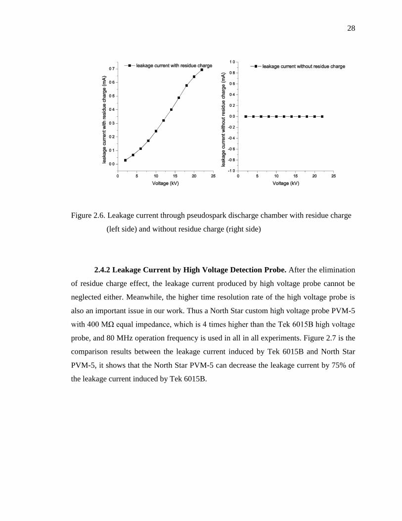
2.4.1 Leakage Current by Residue Charge Effect. A main cause of the leakage
current in the presented system is the “residue charge” produced in the vacuum system
after gas breakdown, instead of the commonly assumed leakage current through high
voltage probe. Such an effect can produce a leakage current 5 - 10 times greater than the
leakage current introduced by high voltage probe, which was expected to be the most
leakage current source in the former work. However, it was found during APLab’s
experimental research that such a residue charge effect can be eliminated by thorough
cleaning of the discharge chamber by acetone in ultrasonic cleaner. Figure 2.6 is the
comparison results on leakage currents between the pseudospark chamber with and
without residue charge effect. As shown in Figure 2.6, the leakage current without high
voltage probe connected become zero after eliminating the residue charge effect.
28
Figure 2.6. Leakage current through pseudospark discharge chamber with residue charge
(left side) and without residue charge (right side)
2.4.2 Leakage Current by High Voltage Detection Probe. After the elimination
of residue charge effect, the leakage current produced by high voltage probe cannot be
neglected either. Meanwhile, the higher time resolution rate of the high voltage probe is
also an important issue in our work. Thus a North Star custom high voltage probe PVM-5
with 400 MΩ equal impedance, which is 4 times higher than the Tek 6015B high voltage
probe, and 80 MHz operation frequency is used in all in all experiments. Figure 2.7 is the
comparison results between the leakage current induced by Tek 6015B and North Star
PVM-5, it shows that the North Star PVM-5 can decrease the leakage current by 75% of
the leakage current induced by Tek 6015B.

29
Figure 2.7. Leakage current flowing through high voltage probe Tek 6015 (left side) and
North Star PVM-5 (right side)
2.4.3 Leakage Current and Instability of Pseudospark Discharge
Configuration. The instability of the electric signals when operating at high voltage is
another problem. Through serial debugging work, it was found that in pseudospark
chamber, there was partial discharge (spark) because of the sharp edge of metal
electrodes and central bore holes under high voltage. Thus all the edges of metal
electrodes are machined to round shape with a 45° angle. Additionally, when the
energetic electrons passing through the central path of pseudospark device, the interaction
of electrons with metal electrode will leave a deposition film on the metal surface of
electrode leading to contamination of electrode.
The contamination of electrode by interaction of energetic electrons passing
through the electron beam path is an important factor leading to instability of discharge
properties after given discharge shot counts. Figure 2.8 shows three electrodes after
various operational time. The left one displays most contamination in the center of
electrode around the central hole of electron beam path after approximately 105 discharge
shots. The middle one also shows contamination on electrode after 104 shots. And the

30
right one is the polished electrode without contamination film. Then in Figure 2.9, the
leakage current caused by electrode contamination under various applied voltages on a
12-gap pseudospark device is presented with polished electrodes and contaminated
electrodes (middle of Figure 2.8) are compared under applied voltages varying from 0-10
kV. As illustrated in Figure 2.9, the leakage current through the pseudospark device with
polished electrodes maintains zero under all investigated voltage values, while the
leakage current through contaminated electrodes keeps increased with increasing voltage.
Thus all the experiments presented in this dissertation were operated in pseudospark
device with polished electrodes. And all the electrodes used in experiments will be
polished after 103 discharge shots.
Figure 2.8. Three electrodes after various operational time

31
Figure 2.9. Leakage current in pseudospark device with polished electrodes and
contaminated electrodes
2.4.4 Transmission of High Voltage Pulse Signal. The coaxial cable with a
characteristic impedance of 50 ohms is usually applied to transmit the nanosecond signal
and the typical structure of a RG 58U coaxial cable is shown in Figure 2.10. However, in
pseudospark discharge experiment, different from the fast pulse signal of low amplitude
value, the high voltage pulse signal requires high dielectric strength of transmission line,
in addition to the time response limit of transmission system. The breakdown of coaxial
cable under high voltage peak between copper wire and external grounding copper mesh
will lead to corona discharge inside the coaxial cable. In addition, insufficient grounding
layer of coaxial cable will cause the leakage of external noise into the transmission line.
All of those will generate inaccuracy of measurements of pseudospark properties.

32
Figure 2.10 Structure of a regular RG 58U coaxial cable [2]
Figure 2.11 and Figure 2.12 shows the 10 continuous shot of pseudospark
breakdown properties (voltage and discharge current) using two different coaxial cables
from the same pseudospark device under the same applied voltage 14 kV. Discharge
properties in Figure 2.11 were obtained using general RG 58U coaxial cable, which has a
single layer grounding mesh and with a voltage rating of 1400 V root-mean-square (RMS)
value. As shown in Figure 2.11, the instability ratio between 10 continuous shots defined
as the difference ratio of the maximum amplitude to the minimum amplitude of discharge
current is 33.8%. Discharge properties in Figure 2.12 were obtained using RG 223
coaxial cable, which has double layer grounding mesh and with voltage rating of 5 kV
RMS value. As illustrated in Figure 2.12, the instability ratio decreases to 3.55% which is
a great performance improvement compared with the performance of RG58 U. All the
experiment results presented in this dissertation work are obtained by RG 223 coaxial
cable.

33
(a) Breakdown voltage waveforms
(b) Discharge current waveforms
Figure 2.11. Discharge properties measured by RG 58U coaxial cable

34
(a) Breakdown voltage waveforms
(b) Discharge current waveforms
Figure 2.12. Discharge properties measured by RG 223 coaxial cable

35
2.5 DIAGNOSTICS OF PSEUDOSPARK DISCHARG PROPERTIES AND
ELECTRON BEAM CHARACTERISTICS
2.5.1 Discharge Properties Diagnostics. As stated in the above section,
pseudospark discharge is a pulse discharge with a time range of 10s ns to 100s ns pulse
width, and several ns rising edge. Thus the response time of the electric measurement
methods and tools are of great importance in such pulse discharge experiments. The
electric measurement system in APLab’s pseudospark experiment consists of the
discharge characteristic measurements and electron beam detectors. The breakdown
voltage of pseudospark discharge is measured by the wide-bandwidth high voltage probe
PVM-5 with a 80 MHz maximum frequency by North Star High Voltage connected to the
hollow cathode directly. A Rogowski coil with 20 MHz rated bandwidth is located in the
discharge loop to measure the discharge current flowing through the energy storage
capacitors.
Figure 2.13 and Figure 2.14 are quantitative results of the response time of the
voltage probe and discharge current transformer presented as the rise time percent
difference for multiple times. The rise time percent difference is defined as the magnitude
of the difference between output signal rise time and input signal rise time divided by the
input signal fall time. A value close to zero is desirable. The test results show that the
error difference ratio of fast rise time varied from 8 ns to 80 ns is below 5% for high
voltage probe and below 10% for Rogowski coil.

36
Figure 2.13. Test results of response time from high voltage probe PVM-5
Figure 2.14. Test results of response time from current transformer

37
The data acquisition is realized by high speed oscilloscope with 500 MHz
bandwidth, 1 G/s sampling rate. The control of oscilloscope readout and data storage is
acquired by a Labview software workbench. Table 2.2 presents the main technical
information of facilities and equipments located in discharge region.
Table 2.2 Main technical specifications of facilities and equipments
Facility and equipment Technical information
High voltage power supply -100kV maximum output, 1mA current limit
High voltage probe High voltage probe-1: Tek P-6015B, 1:1000
attenuation, 3 pF input capacitance, 20kV DC,
40 kV peak, 4 ns usable rise time
High voltage probe-2: North Star PVM-5,
1:1000 attenuation, 12 pF input capacitance,
60kV DC, 100 kV peak, 2.5 ns usable rise time
High speed oscilloscope High speed oscilloscope-1: Tek TDS 2014B,
100 MHz, 1Gs/s
High speed oscilloscope-2: Agilent 54815A, 500
MHz, 1Gs/s
Rogowski current
transformer_1
20 MHz, 20 ns usable rise time,5 kA maximum
input current
Rogowski current
transformer_2
100 MHz, 10 ns usable rise time, 350 A
maximum input DC current, 100 A maximum
input pulse current

38
2.5.2 Intense Pulsed Electron Beam Diagnostics. Pseudospark discharge with
proper configuration is capable of generating intense charge particles, including ion beam
and electron beam. The electron beam produced by pseudospark discharge is a fast pulsed
discharge with time duration of 10s ns ~ 100s ns. In APLab’s pseudospark experiment,
three various types of pulsed electron beam detectors are constructed and calibrated:
Faraday cup with adjustable impedance, Faraday cup with low impedance, and Rogowski
coil. Figure 2.15 shows the Faraday cup and Rogowski coil in the electron drift region.
The technical specifications of Rogowski coil has been presented in Table 2.2 in previous
section as “Rogowski current transformer_2”. And the Faraday cup with adjustable
impedance will be presented in Paper 2 in this dissertation. Only the design procedure
and performance validation of low resistance Faraday cup is presented in this section.
Figure 2.15. Faraday cup and Rogowski coil for electron beam detection
A fast response Faraday cup (FC) with nanosecond response and low resistance of
0.08 ohms is developed to measure the intense electron beam produced by pseudospark
discharge as shown in Figure 2.16. This Faraday cup consists of a collector cup to capture
39
the electron beams, the grounding plate and a low resistance carbon resistor with 0.08
ohms resistance connected between collector cup and grounding plate. This Faraday cup
is constructed based on a semi-rigid coaxial cable with 50 ohms impedance. The inner
conductor of this coaxial cable is joined with the copper collector cup. The coaxial cable
insulated with Teflon coating is passed through the center of carbon resistor, and the
outer grounding mesh of this coaxial cable is connected to the grounding plate. The other
side of this semi-rigid coaxial cable is connected to the N type coaxial connector. Then a
low shunt resistance can be formed between collector and grounding plate as a compact
configuration with minimum stray inductance and reflection of pulse signal.
Figure 2.16. Low resistance Faraday cup electron beam collector
The quantitative results of the response time of the FC are presented as the
attenuation ratio and fall time percent difference for multiple input signal values are
shown in Figure 2.17, Figure 2.18 and Figure 2.19. Figure 2.17 is the output signal from
low resistance Faraday cup probe and input signal from pulse generator. The shunt
resistance can be determined from the attenuation ratio of Faraday cup, defined as ratio of
amplitude of output signal from Faraday cup to the amplitude of pulse generator signal,

40
which is calculated to be 0.086 ohms. Figure 2.18 shows the falling edge of pulse
generator input signal, and the output signal from the presented low resistance Faraday
cup. As illustrated in Figure 2.18, the input signal on the bottom of Figure 2.18 has a 10.7
ns falling edge, while the output signal on top of Figure 2.18 displays a 13.8 ns falling
edge. Then the difference percent of falling edge of output signal from low resistance
Faraday cup and input signal from pulse generator, defined as the magnitude of the
difference between FC signal fall time and input signal fall time divided by the input
signal fall time under various pulse falling time values is shown in Figure 2.19. A value
close to zero is desirable. In Figure 2.19, data are presented for source signal fall times
from 8.6 to 79.6 ns. Within the tested range, the fall time percent difference has a
maximum of 21.8% at the fastest source fall time, 8.6 ns. As source fall time increases,
fall time ratio decreases to below 10% and has a value of 2.26% at 70.8 ns.
Figure 2.17. Output signal of low resistance of Faraday cup (top) and input signal from
pulse generator (bottom)

41
Figure 2.18. Signal falling edge of output signal from Faraday cup (top) and input signal
from pulse generator (bottom)
Figure 2.19. Difference ratio of fall time of output signal from low resistance Faraday cup
and input signal from pulse generator

42
2.6 A SIMPLIFIED TIME DOMAIN REFLECTOMETER SETUP FOR
CALIBRATION OF FAST RESPONSE PROBES
Different types of probes with fast response time below 10 ns lowest limit is
described in previous sections, including Rogowski coils and Faraday cup probes.
Generally, the probes like Rogowski coil current transformer for fast signal
measurements are designed to obtain a 50 ohms standard impedance to match the
impedance of transmission system, in order to minimize the possible reflection and
frequency dispersion of fast signals. However, the characteristic impedance of Rogowski
coil probe will have greater offset due to the variation of permeability of the magnetic
core in Rogowski coil probe. Furthermore, in fast signal measurements, the long coaxial
cable may have discontinuity and damage located at the unknown points. Thus in pulse
signal diagnostics, a simple and efficient tool for troubleshooting and calibration of fast
response probes is very useful in experiments. In industrial applications, a time domain
reflectometer (TDR) is the most efficient method for calibration of probes with 50 ohms
characteristic impedance.
A standard time-domain reflectometer (TDR), as shown in Figure 2.20, is an
electronic instrument used to characterize and locate faults in metallic cables (coaxial
cable or any other electrical path). The basic mechanism of TDR is based on the
transmission line theory illustrated in Figure 2.21. If the characteristic impedances of
source (Zs), load (ZL) and transmission line (Zc) are not matched, only part of the signal
will be transmitted, and the rest will be reflected back. And the reflection coefficient as
presented in [3]:
Then discontinuity on the electric path can be determined from the time difference
between the source pulse, which is the pulse signal on the left side of Figure 2.20 (b), and
the reflected pulse on the right side of Figure 2.20 (b).The location of discontinuity can
be determine by

43
Where is the difference between source signal and discontinuity location, and is
the time difference on oscilloscope between source signal and reflection signal.
(a) Photograph of a commercial TDR
(b) Source signals generated by TDR (left) and the detected reflecting pulse
signal (right)
Figure 2.20. A typical commercial TDR and the detected signals

44
Figure 2.21. Illustration of transmission line with source (Zs) and load (ZL)
Although TDR is convenient for calibration of impedance discontinuity on signal
transmission line, a commercial TDR is usually expensive (thousands dollars). Thus in
our experiments, a simplified TDR setup by oscilloscope, pulse generator and RG 58U
coaxial cable is constructed to realize the basic functions of TDR. The schematic and
photograph of this simplified TDR setup are illustrated in Figure 2.22 (a) and (b).
(a) Schematic of TDR setup
Figure 2.22. Schematic (a) and photograph (b) of the simplified TDR setup
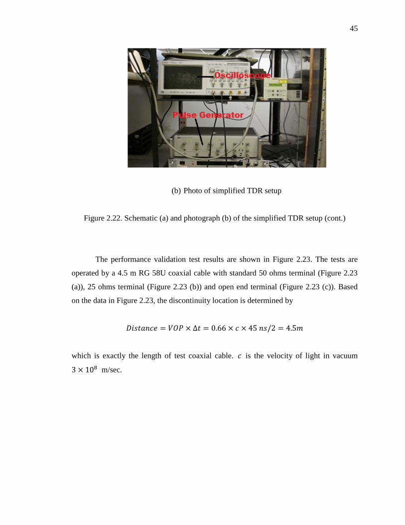
45
(b) Photo of simplified TDR setup
Figure 2.22. Schematic (a) and photograph (b) of the simplified TDR setup (cont.)
The performance validation test results are shown in Figure 2.23. The tests are
operated by a 4.5 m RG 58U coaxial cable with standard 50 ohms terminal (Figure 2.23
(a)), 25 ohms terminal (Figure 2.23 (b)) and open end terminal (Figure 2.23 (c)). Based
on the data in Figure 2.23, the discontinuity location is determined by
which is exactly the length of test coaxial cable. is the velocity of light in vacuum
m/sec.

46
(a) Standard 50 ohms terminal
(b) 25 ohms terminal
Figure 2.23 Performance validation of simplified TDR setup

47
(c) Open-end terminal
Figure 2.23. Performance validation of simplified TDR setup (cont.)
This simplified TDR setup has been applied in the calibration of fast response
probes used in pseudospark discharge experiments and the results are shown in Figure
2.24. Figure 2.24 (a) on the top is the test results of Rogowski coil probe NO.1 for
discharge current measurement. Figure 2.24 (b) on the bottom shows the test results of
Faraday cup probe with 50 ohms terminal. Both results show that there are some
impedance mismatching on two probes, but the mismatching amplitude is less than 15%.

48
(a) TDR test results of Rogowski coil probe
(b) TDR test results of Faraday cup probe
Figure 2.24. Test results of Rogowski coil probe and Faraday cup probe by this TDR
setup

49
BIBLIOGRAPHY
[1] Miller, R.B., 1982 An introduction to the physics of intense charged particle
beams (New York, N.Y.: Plenum Press)
[2] Website information:
http://www.webdesigningwebertizers.com/finalproject2/cabling.html
[3] D. M. Pozar, Microwave Engineering, 3rd ed. (John Wiley and Sons, Inc., 2005).

50
PAPER
I. EXPERIMENTAL INVESTIGATION OF FORMATION TIME IN
SINGLE-GAP PSEUDOSPARK DISCHARGE
Hu, Jing and Joshua L. Rovey
ABSTRACT
Experiment results on the formation of pseudospark discharge in single-gap
device are presented. The formation process is investigated by capacitive probes and
shows two phases: a slow initiation phase and a fast current increasing phase. The
initiation of the discharge is found to be synchronous with a high speed ionization wave
propagating from cathode to anode. Transition to the high current phase is initiated when
the ionization front reaches the anode side. The experimental results on four different gap
widths are presented under different pressures. The characteristic time of the initiation
phase of the discharge is decreased with increasing pressure in all four gap widths. The
mean velocity of the observed ionization front is varied from to
under the investigated pressures. In four gap widths, the velocity of the
ionization front can be fitted by one given curve as an exponential decline function of
E/P.
1. INTRODUCTION
The pseudospark discharge was first discovered in the late 1970’s, as an axially
symmetric, high voltage gas discharge operating at low pressure regime located on the
left hand side of the Paschen curve, which is usually initiated from a hollow cathode
discharge (HCD) [1-5]. The fundamental discharge configuration consists of planar
anode and hollow cathode, or multi-gap electrodes, with a central hole located in the
electrodes. The central hole in the electrodes makes the effective distance of the
51
discharge path a maximum in the region of the bore hole on the axial center of the
electrodes and cathode cavity.
Pseudospark discharge has many unique properties. It is a pulsed gas discharge
that can obtain tens to hundreds of kV voltage hold-off capability and kA discharge
current during total time of discharge of tens to hundreds ns, and several ns rise time.
Physical volume of pseudospark device, including discharge gap and hollow cathode, is
tens of cm3. These characteristics make it suitable for a variety of applications, including
high power switches [1-6], high energy e-beam sources [2,5,7,8], and in Ref [2,9], pulsed
laser oscillations were observed in an Ar-He pseudospark discharge. Most of the reported
applications, especially the switch applications and laser oscillation, require knowledge
of time-dependent characteristics of the discharge formation and development, which
reveals a number of complex phenomena to be explained.
The temporal development of a pseudospark discharge can be separated into four
different phases [5-6]:
1) Predischarge (ignition of the pseudospark);
2) Hollow cathode discharge;
3) High current main discharge;
4) Decay of the discharge plasma.
The voltage-current characteristic and build-up of the highly conductive plasma of
the discharge are of great interest because that part of the discharge is most closely
associated with its applicability in a pulsed power system. In Ref [3-5], it is stated that
phase 1 is related to the delay time between trigger and the onset of applied potential on
discharge devices. And the repetition rate of the pseudospark device is mainly dependent
on the decay process of plasma during phase 4 [7]. Comparatively, the exact mechanism
of the hollow cathode phase (phase 2) and superdense high current main discharge phase
(phase 3) is not fully understood yet. However, phase 2 and 3 have been considered to
comprise multiple complex processes by a great number of previous studies [5,10,12].
For example, in [5], a physical model of prebreakdown in the hollow cathode discharge is
established based on numerical simulation results. In this work, it was put forward that
the prebreakdown phase of the pseudospark is related to the buildup of a positive space
charge in the hollow cathode mainly due to ionization by electron impact. In [10], the

52
simulations based on a hybrid fluid-particle model were developed to describe the
evolution of the initiation phase of pseudospark discharges. The simulation results
presented in [10] shows that the pseudospark discharge is initiated by the rapid
multiplication of electrons in hollow cathode region, and the current rise is characterized
by the expansion of plasma from the hollow cathode and the enhance electron emission
from the cathode.
Besides the research studies on the fundamental physical mechanisms of
discharge evolution, the industrial applications requires more concerns on device
performances in the current and charge transfer capability, and high current rising
capability (1010
A/sec~1011
A/sec) of pseudospark. However, compared with the
extensively qualitative and quantitative experimental investigations and physical model
on the high pressure spark-gap switches in various technological focuses [1,11,13].
investigations of pseudospark discharge as switching devices are still not well determined,
including the formation and initiation of plasma, build-up time to obtain highly
conductive phase, total rise time to maximum peak current, time-varied oscillation period
and frequency, modeling and determination of plasma resistivity and inductance, which
are of great importance in order to verify discharge formation models and optimize the
performance of this discharge device [1,5,11,13].
This paper presents the detailed experimental investigations of the time-dependent
characteristics of single gap pseudospark discharge device. The formation time of the
initiation of discharge current increase and build-up of highly conductive channel during
the high current main discharge phase (phase 3) are the main focus in this work for its
importance in the performance as switching device [1,3,11]. The formation time of
discharge starting from initiation to maximum breakdown and its dependence on gas
pressures are investigated in single-gap device with four various width of gap region.
And the discharge development is temporally correlated with movement of a space
charge front detected by two capacitive probes. The main emphasis of this paper is on the
problem of discharge mechanism in pseudospark discharge device, and the dependence of
discharge formation on external parameters, such as geometric factors and gas pressure.
Additionally, a discussion of an ionization front model is proposed to explain the initial
53
formation and time evolution of the plasma column and ionization wave inside the
device.
This work is organized into the following sections: a detailed introduction to the
current pseudospark experiment setup and measurement methods is presented in Sec II.
The experiment investigation results of discharge properties on gap space and neutral gas
pressure are presented and summarized in Sec III. Finally, discussions and conclusions
based on the experimental results and comparison with the results in related references
are summarized in the last section.
2. EXPERIMENT SETUP
The single-gap pseudospark discharge chamber is shown in Figure 1. It consists
of a cylindrical hollow cathode and grounded anode insulated by a pyrex disk. Anode,
cathode and insulator have 22 mm outer diameter and 2 mm on-axis hole for electron
beam extraction. The length of cathode cavity is 25 mm and the thickness of hollow
cathode cavity and anode electrode is 1 mm. The gap distance between a pair of
electrodes can be varied from 2 mm to 14 mm. Two 390 pF resin-dipped ceramic
capacitors were connected between the anode and cathode symmetrically for energy
storage. The material of all electrodes is stainless steel.
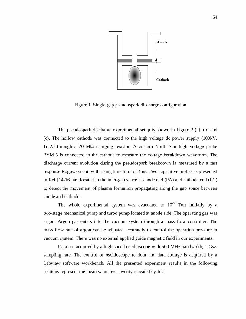
54
Figure 1. Single-gap pseudospark discharge configuration
The pseudospark discharge experimental setup is shown in Figure 2 (a), (b) and
(c). The hollow cathode was connected to the high voltage dc power supply (100kV,
1mA) through a 20 MΩ charging resistor. A custom North Star high voltage probe
PVM-5 is connected to the cathode to measure the voltage breakdown waveform. The
discharge current evolution during the pseudospark breakdown is measured by a fast
response Rogowski coil with rising time limit of 4 ns. Two capacitive probes as presented
in Ref [14-16] are located in the inter-gap space at anode end (PA) and cathode end (PC)
to detect the movement of plasma formation propagating along the gap space between
anode and cathode.
The whole experimental system was evacuated to 10-5
Torr initially by a
two-stage mechanical pump and turbo pump located at anode side. The operating gas was
argon. Argon gas enters into the vacuum system through a mass flow controller. The
mass flow rate of argon can be adjusted accurately to control the operation pressure in
vacuum system. There was no external applied guide magnetic field in our experiments.
Data are acquired by a high speed oscilloscope with 500 MHz bandwidth, 1 Gs/s
sampling rate. The control of oscilloscope readout and data storage is acquired by a
Labview software workbench. All the presented experiment results in the following
sections represent the mean value over twenty repeated cycles.

55
(a) Capacitive probes constructed on flexible PCB film
(b) Pseudospark chamber with two capacitive probes
Figure 2. Capacitive probes and experiment setup of single-gap pseudospark discharge
experiment

56
(c) Experiment setup of pseudospark discharge experiment
Figure 2. Capacitive probes and experiment setup of single-gap pseudospark discharge
experiment (cont.)
3. EXPERIMENT RESULTS
3.1 TEMPORAL EVOLUTION OF DISCHARGE IN SINGLE-GAP
PSEUDOSPARK DEVICE
Figure 3 shows the self-breakdown voltage and discharge current obtained from a
single-gap pseudospark device with a gap thickness of 10 mm at 35 mTorr. As shown in
Figure 3, during the increase of voltage applied on the pseudospark device (before 150 ns
in Figure 3 and Figure 4), the high voltage capacitor is charging continuously charged
until the electric field strength between anode and cathode is high enough to reach the
“breakdown” value at the given pressure, then the conducting plasma discharge forms
between anode and cathode. Charge is carried through the plasma until the energy storage
by the capacitors is drained, at which point the plasma discharge is extinguished and the
capacitor is recharged for the next shot (after 300 ns in Figure 3). Thus the pseudospark
discharge in this experiment can operate under single mode or repetitive mode. All the
data presented in this work is obtained in single mode.

57
The time duration between 150 ns and 300 ns is the main discharge starting from
increase of discharge current. After the voltage breakdown, the current and the voltage
signals show damped oscillations, which is the typical characteristic for self-sustained
pulsed gas discharges initiated from a hollow cathode discharge (HCD) [6,17]. In Ref
[17], fast shutter camera photos showed that the development of the plasma column is
closely related to the first half-wave of the discharge current, while the damped current
oscillations after the voltage breakdown are related to the external circuit parameters [17].
Thus in this work, the rise time and oscillation period to obtain the maximum discharge
current in the first half-wave was our main focus.
Figure 3. Breakdown voltage (top) and current (bottom) waveform traces
In addition to the subsequent damped oscillations, Figure 3 also shows two
different phases in the “rising” edge on the first half-wave of the discharge current
starting from the initiation of the discharge. Phase I is a slow current increasing phase and

58
phase II is the fast high current build-up phase. These two different phases can be more
clearly presented by time-dependent dI(t)/dt illustrated in Figure 4. As shown in Figure 4,
starting from 150 ns, the dI(t)/dt has a comparatively slow and flat current rising rate until
170 ns, from A/sec to A/sec within 20 ns. After that the temporal
current rising rate keeps a fast increasing trend on the rising edge of the discharge current
until reaching a maximum, increasing from A/sec to A/sec in 13
ns.
Figure 4. Discharge current and time-dependent dI(t)/d(t) corresponding to Figure 3
Similarly, in Ref [6,17], the two phases on the rising edge of discharge waveform
were also presented and temporally related with fast shutter camera photographs in a
similar type of HCD like the pseudospark. In Ref [6], it was shown that the phase I, slow
current increasing phase was synchronous with the movement of an ionization wave front
from the cathode to the anode, followed by a sudden increase of discharge current. And

59
the fast ionization wave was observed to propagate from cathode to anode with a velocity
of m/s. In order to investigate the presence of a fast ionization wave propagation
mode in a single-gap pseudospark discharge device, and its correlation with initiation of
discharge, two capacitive probes were located on the inter-gap space to detect the
formation and movement of plasma and the ionization wave.
The construction of capacitive probes in our work has the same configuration as
the capacitive probe array used in Ref [14-16]. The mechanism and physical
interpretation of capacitive probes have been discussed in detail in Ref [14-16]. Simply
speaking, the rise of the capacitive probe signal shows that a plasma has formed at the
location of the corresponding probe. The capacitive probe signals for the same shot as
Figure 3 and Figure 4 are shown in Figure 5, with the rising edge of discharge current,
signals of capacitive probe located near cathode (PC), and capacitive probe located near
anode (PA).
As illustrated in Figure 5, the capacitive probe signals show that there is a
negative polarity signal moving from cathode to anode side in the discharge gap space.
Furthermore, comparing the starting time of phase I and phase II with the peak time of
the two cathode probe signals, it shows that phase I corresponds with the time difference
between the two probe signal peaks. This observation is identical with the experiment
results presented in Ref [6] and the qualitative model of electric breakdown assisted by
ionization wave propagation [18]. In Ref [6], based on the presented results (Figure 4 and
Figure 5 in Ref [6]), the initiation phase (phase I in our work) starts synchronously with
an ionization front moving from cathode to anode with slowly increasing discharge
current. The propagation velocity of this front was estimated as m/s. The ionization
front stops in front of the anode end then the fast discharge current increasing starts at the
same time [6]. These observations indicate that the initiation of the pseudospark
discharge is assisted by the propagation of a moving space-charge-creating front, and
when this front stops at anode backside, the fast high current phase is initiated.

60
Figure 5. Time-related signal of discharge current, capacitive probe on cathode side (PC)
and capacitive probe on anode side (PA)
3.2 CHARACTERISTIC TIMES IN SINGLE-GAP PSEUDOSPARK DEVICES
WITH VARIOUS GAP SPACE
The single-gap pseudospark device as illustrated in Figure 1 consists of grounded
anode and hollow cathode of given length. The external capacitance, length of cathode
cavity, and radial diameter of the device remain constant among all the experiments
presented.

61
3.2.1 Total Rise Time from Initiation of Breakdown to Maximum Current.
Figure 6 shows the time duration of the rising edge of the discharge current in a
single-gap pseudospark device with different gap width. For the same pressure, the rise
increases with wider gap width, equivalent to a “slower” build up process of the highly
conductive plasma channel on the pseudospark axis. Meanwhile, the variation of
discharge current magnitude in the devices with various gap width is most related with
the applied voltage on the discharge gap, corresponding to the given gap width and
operation pressure, which will be discussed in the following Section 3.2.3.
The total rise time for different ambient pressures obtained in single-gap
pseudospark device with gap width d = 2mm, 4mm, 6mm and 14mm is presented in
Figure 7. The rise time starting from breakdown front to the maximum current peak
decreases with ambient pressure in a single gap device. Furthermore, the effect of
pressure on rise time becomes more obvious in a device with wider gap. In pseudospark
device with 14mm gap width, the rise time in 15 mTorr argon is 83.4 ns, 514.8% higher
than the rise time in 110 mTorr, the maximum pressure under which the pseudospark can
operate with a 14 mm gap. But in a pseudospark device with 2mm gap width, the rise
time in 15 mTorr is 208% higher than the rise time in the maximum operation pressure of
240 mTorr.

62
Figure 6. First half-wave discharge current in various single-gap pseudospark devices

63
Figure 7. Rise time in various single-gap pseudospark devices
3.2.2. Characteristic Time of Slower Initiation Phase and Fast Highly
Conductive Phase. As stated in previous sections, there are two different phases on the
rising edge of discharge waveform starting from the initiation of main discharge: a slow
current rising phase (phase I) and the following fast high current build-up phase (phase
II), as marked in Figure 3 and Figure 4. In Figure 5, the starting point of phase I and
phase II are synchronous with the propagation of a moving space-charge-creating front
from cathode to the anode backspace. And Figure 6 shows that under the same ambient
pressure, the time duration of phase I is increased in the wider discharge gap. Thus in this
section, the characteristic time duration of phase I and II are presented in single-gap
pseudospark devices of various gap space widths.
Figure 8 is the characteristic time of phase I versus pressures in various gap width
and Figure 9 shows the time duration of phase II. In order to illustrate the proportion of
phase I and phase II compared with total time of rising edge, data in Figure 8 and Figure
9 are presented on the same axis scale as Figure 7.

64
As illustrated in Figure 8, the time duration of phase I shows a similar variation
trend as total rise time with ambient pressure. For a discharge gap of 14 mm space width,
time duration of phase I decreases from 71.8 ns at 15 mTorr to 6.4 ns at 110 mTorr. In
discharge gap of 2 mm width, time duration of phase I decreases from 9.7 ns at 15 mTorr
to 1.5 ns at 220 mTorr. In the higher pressure region, the time difference of phase I
becomes lower for various gap space widths.
Figure 8. Characteristic time of phase I under various pressures

65
Figure 9. Characteristic time of phase II under various pressures
Compared with phase I, the time duration of phase II does not vary as much as
phase I in a single gap device as pressure increases. The time duration of phase II is
assumed to be most related with the impedance of external circuit, including ohmic
resistance, stray inductance and dynamic inductance of the discharge loop, and the
capacitance [1,11-13]. The stray inductance of the presented discharge loop in this work
can be measured by a RLC meter and calculated from geometric dimensions by the
formula [19].
(1)
Where N is the number of loop, w is the length of inductance loop, is the wire
radius and is the relative permeability of the medium. And the results show the stray
inductance of the circuit is approximately 40~50 nH. With the 780 pF external
capacitance, the generated quarter damping oscillation period is estimated to
which equals to 18~20 ns. This result is close to the time duration of phase II in our work,

66
which suggests that the time duration of phase II is mainly determined by the R, L, C
parameters of the external circuit and discharge loop. Although the variation of time
duration of phase II is not so great as phase I, it still can be seen in Figure 9 that the time
of phase II is longer in 14 mm gap than shorter gap width, which is mainly caused by
higher resistance and inductance of plasma column in longer discharge gap [1,11,13,17].
The exact values of ohmic resistance, dynamic inductance of discharge loop, including
the plasma column, must be determined by dynamic measurement and analysis methods
as shown in [13,20], etc., which are beyond the topic of this work.
3.2.3 Propagation Speed of Ionization Front in Single-gap Device. The time
evolution of initiation phase I, as presented in Figure 8, shows the propagation of an
ionization front, which varies with ambient pressure [14-15,18,21], electric field, and
propagation path. The characteristic mean speed of the ionization front is determined by
the gap space width and the time duration of initiation phase in this section. The
propagation speed of the ionization front in single-gap device with various gap widths
under ambient pressures is presented in Figure 10. This propagation velocity is calculated
as:
(2)
where d is the gap space width and t is the time duration of phase I presented in
Figure 9.

67
Figure 10. Propagation speed of ionization front
According to the results in Figure 10 in a given gap device with given gap space
width, the velocity is increased with pressure, since the velocity of the ionization front is
promoted by the effective ionization frequency [18,21], which increases with ambient
pressure on the left side of Paschen curve. Considering the comparison of this velocity of
the ionization front in pseudospark device with various gap widths, the dependency of the
velocity of ionization front on the applied potential in the gap region and the generated
electric field is another important parameter. Figure 11 shows the breakdown voltage of
the single-gap pseudospark devices with four gap widths presented in this work. As
illustrated in Figure 11 and some other work [22-24], in the low pressure region on left
side of Paschen curve, the breakdown voltage of pseudospark is decreased with increase
pressure in a single device. And in the device with different geometric configurations, the
stable operational pressure region of the pseudospark discharge gap is also affected by
the gap width (d in Figure 1) [22-24], which also directly determines the magnitude of
electric field inside the gap region.

68
Figure 11. Breakdown voltage versus pressure in four devices
The breakdown voltage versus pressure in pseudospark device with different
geometric factors can not be described by a general scaling law like Paschen’s law yet
due to the geometry complexity in pseudospark device, including hollow cathode
structure and common central hole in electrode side [1,5,23-24]. However, it should be
noted that the dependence of ionization frequency on reduced field value E/P can be
considered instead of the dependence on electric field or pressure [1]. Considering the
effect of various gap widths, the evolution of the speed of ionization front can be
represented best by the dependence on the value of E/P, where E is the static electric field
expressed in V/cm and P is the neutral gas pressure expressed in Torr as shown in Figure
10 and Figure 11. Based on the data presented in Figure 10 and Figure 11, the velocity of
the ionization front obtained with all four gap widths can be fitted by a function of E/P
with the following form:
(3)
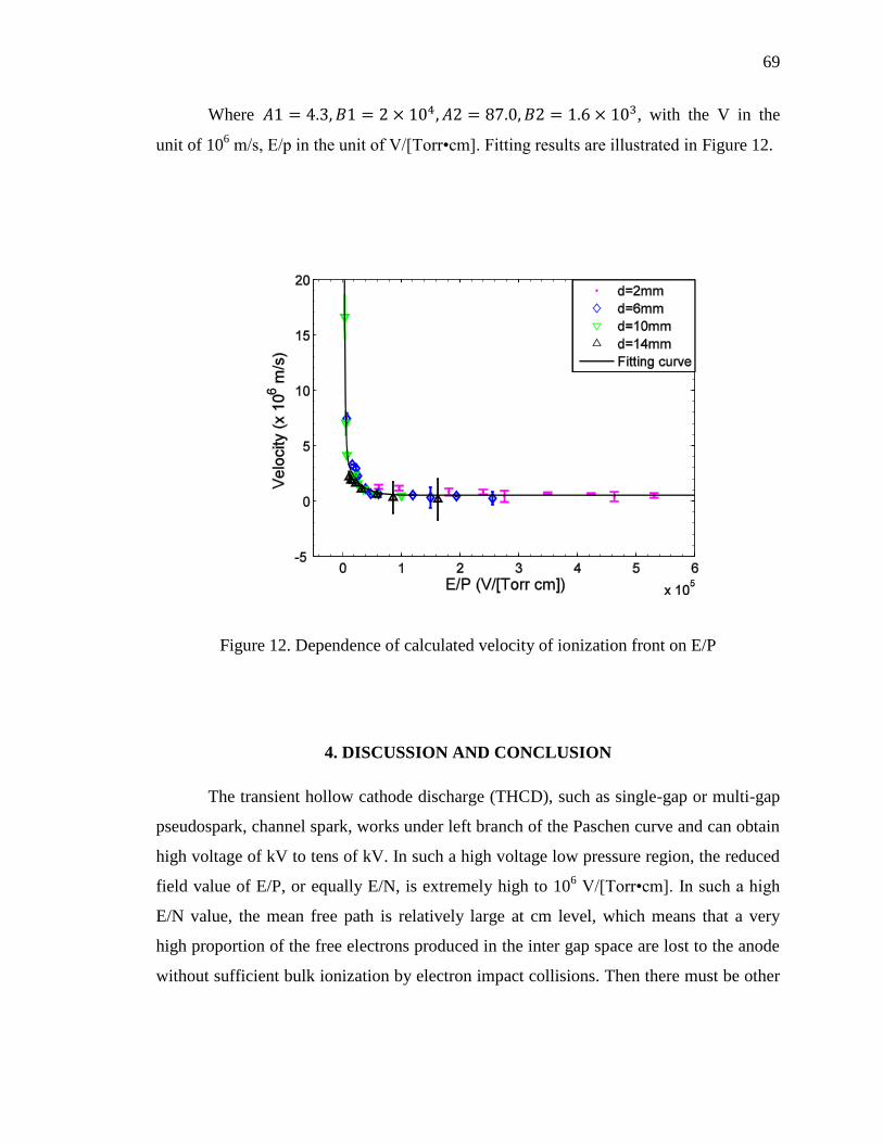
69
Where , with the V in the
unit of 106 m/s, E/p in the unit of V/[Torr•cm]. Fitting results are illustrated in Figure 12.
Figure 12. Dependence of calculated velocity of ionization front on E/P
4. DISCUSSION AND CONCLUSION
The transient hollow cathode discharge (THCD), such as single-gap or multi-gap
pseudospark, channel spark, works under left branch of the Paschen curve and can obtain
high voltage of kV to tens of kV. In such a high voltage low pressure region, the reduced
field value of E/P, or equally E/N, is extremely high to 106 V/[Torr•cm]. In such a high
E/N value, the mean free path is relatively large at cm level, which means that a very
high proportion of the free electrons produced in the inter gap space are lost to the anode
without sufficient bulk ionization by electron impact collisions. Then there must be other

70
charge multiplication and ionization processes causing the initiation of the high current
discharge.
Based on our experiment results, the propagation of an ionization front is
synchronous with the initiation of a pseudospark discharge. When this front stops at
anode backspace, the discharge transits to the high current phase. Such an ionization front
is considered to be stimulated by the electron beam injected through the anode-cathode
gap space, which is initiated from the hollow cathode region [5,6,10,14-15,17]. The
characteristic time of the propagation of this ionization front was investigated under
ambient pressures and in various inter gap space width in our work. Results show that the
characteristic time of the initiation phase and velocity of the ionization front are affected
directly by the pressure of gas and reduced electric field. Furthermore, the calculated
propagating velocity in four different gap widths can be fitted in the same exponential
decay function of E/P, which presents a steep decrease of velocity of ionization front with
lower neutral gas density, and higher E/P value. Qualitatively, this trend is consistent
with the variation of ionization frequency on the left side of the Paschen curve [18,21],
which increases with gas pressure and decreases with E/P.
Furthermore, in many applications, such as pulse technology, laser drive, etc., the
fast total rising time obtained by the discharge device is a very important technical focus.
Our experiment results show that the total time for a single-gap discharge device to reach
high current consists of a slow initiation phase and a fast current rising phase. The former
phase has been investigated by capacitive probe experiments. The latter phase is
considered to be related to the equivalent inductance and resistance of the plasma column
formed during the main discharge phase [1,6,11,17]. Our results also shows that the
characteristic time of phase II is identical with the falling time of the first half wave of
discharge current. The exact and time-resolved determination of the effects of ohmic
resistance, time-varied inductance of plasma column and capacitance of the discharge
configuration should be determined by other dynamic measurement methods, such as
transmission line method as presented in [13,20].
Meanwhile, it should be clarified that the discussion of hollow cathode effect is
not taken into discussion in this work. Based on the previous work performed by Mittag
in [5], Boeuf and Pitchford [10], the hollow cathode effect plays an important role in the

71
phase prior to the high current main discharge (described as phase 2 in the Introduction).
In this phase, the expansion of plasma in the hollow cathode region, the large
multiplication of electrons due to the pendulum movement in the hollow cathode and the
buildup of sheath in this region have been discussed in [5,10]. The limit of the capacitive
probe method implies that it may be not appropriate to determine the plasma formation or
ionization events in the hollow cathode region because of the rapid plasma expansion in
radial direction [25]. So in our work the hollow cathode configuration remains the same
in all the presented work and only the propagation of ionization front in the internal gap
region are under investigation. The hollow cathode effect on the time-dependent
discharge parameters should be determined by other methods, such as optical and spectral
measurements as performed in [26].
REFERENCES
[1] Schaefer G, Kristiansen M and Guenther A (eds) 1990 Gas Discharge Closing
Switches (New York, N.Y.: Plenum Press)
[2] Frank K and Christiansen J 1989 IEEE Trans. Plasma Sci. 17 748
[3] Tkotz R, Gortler A, Christiansen J, Dollinger S, Frank K, Heine F, Herleb U,
Insam S, Kowalewicz R, Mehr T, Poister A, Prucker U, Schlaug M and
Schwandner A 1995 IEEE Trans. Plasma Sci. 23 309
[4] Jiang C, Kuthi A and Gundersen M A 2005 Appl. Phys. Lett. 86 024105
[5] Gundersen M A and Schaerfer G (eds) 1990 Physics and Applications of
Pseudosparks (New York, N.Y.: Plenum Press)
[6] Frank K, Stark R, Christiansen J, Felsner P, Gortler A, Hoffmann D, Prucker U,
Schwandner A, Stetter M, Tkotz R and Urban J 1997 IEEE Trans. Plasma Sci. 25
740
[7] Rosier O, Apetz R, Bergmann K, Jonkers J, Wester R, Neff W and Pankert J
2004 IEEE Trans. Plasma Sci. 32 240
[8] Gastel M, Hillmann H, Muller F and Westheide J 1995 IEEE Trans. Plasma Sci.
23 248

72
[9] Christiansen J, Lieser N, Rath W, Steudtner W, Rozsa K, Janossy M, Apai P and
Mezei P 1985 Optics Comm. 56 39
[10] Boeuf, Jean-Pierre, Pitchford, Leanne C 1991 IEEE Trans. Plasma Sci. 19 286
[11] Martin J C 1996 J.C.Martin on Pulsed Technology, (New York, N.Y.: Plenum
Press)
[12] Larigaldie, Serge 1995 IEEE Trans. Plasma Sci. 23 362
[13] Sorensen T P and Ristic V M 1977 J. appl. Phys. 48 114
[14] Favre M, Wyndham E, Lenero A M, Suzuki F, Valenzuela J, Avaria G, Ruiz M,
Bhuyan H, Chuaqui H and Choi P 2008 Plasma Sources Sci. Technol. 17 024011
[15] Favre M, Choi P, Chuaqui H, Mitchell I, Wyndham E and Lenero A M 2003
Plasma Sources Sci. Technol. 12 78
[16] Favre M, Chuaqui H, Lenero A M, Wyndham E and Choi P 2001 Rev. Sci.
Instrum. 72 2186
[17] Dewald E, Frank K, Hoffmann D H H and Tauschwitz A 2002 IEEE Trans.
Plasma Sci. 30 363
[18] Lagarkov A N and Rutkevich I M 1994 Ionization Waves in Electric Breakdown
of Gases (New York : Springer-Verlag)
[19] Walker C S 1990 Capacitance, Inductance, and Crosstalk Analysis (Norwood,
MA : Artech House)
[20] VanDevender J.P 1978 J. Phys, D: Appl. Phys. 49 2616
[21] Sinkevich O A and Gerasimov D N 2000 J. Phys, D: Appl. Phys. 33 54
[22] Rhee M J, Liu C J 1994 Appl. Phys. Lett. 65 3314
[23] Rhee M J, Ding B N 1992 Phys. Flu. B. 4 764
[24] Yin H, He W, Cross A W , Phelps A D R , Ronald K 2001 J. appl. Phys. 90 3212
[25] Choi P, Favre M 1994 Rev. Sci. Instrum. 65 2281
[26] Stetter M, Felsner P, Christiansen J, Frank K, Goertler A, Hintz G, Mehr T, Stark
R, Tkotz R 1995 IEEE Trans. Plasma Sci. 23 283

73
II. FARADAY CUP WITH NANOSECOND RESPONSE AND ADJUSTABLE
IMPEDANCE FOR FAST ELECTRON BEAM CHARACTERIZATION
Hu, Jing and Joshua L. Rovey
ABSTRACT
A movable Faraday cup design with simple structure and adjustable impedance is
described in this work. This Faraday cup has external adjustable shunt resistance for
self-biased measurement setup and 50Ω characteristic impedance to match with 50 Ω
standard BNC coaxial cable and vacuum feedthroughs for nanosecond-level pulse signal
measurements. Adjustable shunt resistance allows self-biased measurements to be
quickly acquired to determine the electron energy distribution function. The performance
of the Faraday cup is validated by tests of response time and amplitude of output signal.
When compared with a reference source, the percent difference of the Faraday cup signal
fall time is less than 10% for fall times greater than 10 ns. The percent difference of the
Faraday cup signal pulse width is below 6.7% for pulse widths greater than 10 ns. A
pseudospark-generated electron beam is used to compare the amplitude of the Faraday
cup signal with a calibrated F-70 commercial current transformer. The error of the
Faraday cup output amplitude is below 10% for the 4 to 14 kV tested pseudospark
voltages. The main benefit of this Faraday cup is demonstrated by adjusting the external
shunt resistance and performing the self-biased method for obtaining the electron energy
distribution function. Results from a 4 kV pseudospark discharge indicate a
“double-humped” energy distribution.
1. INTRODUCTION
A Faraday cup (FC) is a beamline diagnostic that is used to measure the electric
parameters of electron beams, such as beam current. The structure and parameters of a

74
FC can be optimized for the characteristics of various electron beam types. In addition to
the traditional design considerations of FCs, such as electron emission, electron stopping
range, and particle back-scattering, the development of high voltage pulsed power
sources places new requirements on effective passive probes. For instance, fast response
time and movable configurations to study the characteristics and evolution of electron
beams at various locations. In this work, a FC with sub-nanosecond response time and
adjustable resistance for self-biased measurement is presented.
The FC described in this paper is used to measure the intense electron beam
produced by a pseudospark discharge, which is a type of high voltage pulsed discharge
with rise time on the order of nanoseconds and currents in the range of amps to hundreds
of amps. This FC is also used to determine the time-resolved electron energy distribution
function by the self-biased method [1-2], which requires that the FC have adjustable
impedance. Although there are various passive probes for pulsed electron beam
diagnostics that have been published formerly [3-5], in these designs for pulse
applications, in order to minimize the stray inductance, which is important for
nanosecond-level pulse signal, the outer conductor of the transmission line is connected
with the inner conductor by a fixed shunt resistor to form a compact assembly. Thus, the
impedance of the FC is not adjustable and the self-biased resistance cannot be changed to
capture electrons of different energy level. The design presented here provides a new
contribution in the fabrication of FCs with subnanosecond response time, and the
adjustable shunt resistor configuration for self-biased electron energy measurement [1-2].
In our design, the grounding conductor is not connected with the inner conductor by a
fixed resistor, so the FC can be setup as a movable detector to measure electron loss and
energy spread along the drift path of the electron beam.
2. DESIGN PROCEDURE
The FC is designed to measure an electron beam pulse signal with duration on the
order of 50 nanoseconds and rise time shorter than 10 nanoseconds. For such a short
pulse, the maximum signal frequency can be up to 0.1~1 GHz [6], thus the characteristic

75
impedance and the impedance matching between the FC and test network are important
design considerations. A schematic of the design is shown in Figure 1 and the
corresponding transmission line model is illustrated in Figure 2. The cup core is formed
by a changeable carbon collector. The bottom of the FC is machined with a small step
junction structure to permit a short center line of the coaxial cable passing through. The
carbon collector is well-insulated from the external grounding conductor by a 7.6 mm
thickness insulating layer, and the resistance of the FC is adjusted external to the vacuum
system. The FC is modeled as a short transmission line terminated by standard RG-58U
BNC 50Ω coaxial cable. The signal source is the pulsed current of the electron beam.
Based on basic transmission line theory [7], the FC can be considered a parallel planar
waveguide configuration with characteristic impedance given by Equation (1). By
selecting appropriate values for the radial dimension (w) and the distance between the
carbon collector and grounding layer (d), the FC can be designed to have a matched
characteristic impedance and minimum reflection and dispersion of high frequency
signals.
(1)

76
Figure 1. Schematic drawing of the FC (all units are in mm)
Input electron
pulse
Faraday cup modeled as
double-line transmission
configurationStandard 50 ohms coaxial
cable
Transmission line-1 Transmission line-2Source end ……………..
Load
Figure 2. The transmission line model of the FC configuration

77
Furthermore, in the self-biased FC design, the dielectric strength between carbon
conductor and grounding layer is another important consideration because there could be
a high self-biased voltage pulse up to 1-10 kV between them during operation. Under
such a high voltage pulse, partial discharge and spark may take place between carbon
conductor and grounding, and at the air gap between their edges. The radial dimension of
the carbon cup w is limited by the geometric dimensions of the experiment system, such
as vacuum port, drift tube, etc. The dielectric strength is then set to yield a
impedance match and hold enough high potential difference between carbon conductor
and grounding.
Based on all above design considerations, in our FC structure, the insulator layer
is acrylic sheet with a relative permittivity of 2.7 ( ) instead of the more
commonly used Teflon ( ), in order to meet the requirements from
dielectric strength and vacuum tube and port limit. Thus the ratio of w/d should be 4.6 to
achieve a impedance match. In our design, the optimum d is 7.6 mm and w is 35
mm.
The grounding conductor of the BNC cable is connected with both the
external grounding conductor of the FC (insulating layer) and the linear motion arm to
minimize stray inductance. A short coaxial cable carries the signal out through the
vacuum feedthrough and connects with an external self-biased test circuit consisting
of self-biasing resistor Rp and current view shunt resistor Rs [1-2]. The whole system is
designed to obtain the impedance matching at both the source terminal and load
terminal through the FC. And since the impedance matches at each terminal, the internal
conductor does not have to be connected with the grounding conductor through any low
inductance shunt resistor to minimize the pulse signal dispersion and reflection. Then the
external self-biased resistor can be changed externally to obtain the electron beam current
with different energy [2]. In the experiments presented in this work, there is no negative
biased metallic shielding grid located in front of the cup front face since the calculated
displacement current in our experiment operations is lower than 3% of the total electron
beam current. A schematic of this self-biased method and the experiment setup including
the discharge chamber are illustrated in Figure 3.

78
Figure 3. The schematic of self-biased FC set-up (not to scale)
3. EXPERIMENT RESULTS
Three main experiments are conducted. First, the response time of the FC is
validated by comparing with a known test signal. Second, the current amplitude is
validated by comparing with a calibrated current transducer. Finally, the main benefit of
the FC is demonstrated through external adjustment of the shunt resistance to acquire the
electron energy distribution function using the self-biased method.
3.1 RESPONSE TIME
To test the response time of the FC circuit, the front surface of the FC collector is
connected to a pulse generator with internal load. The FC is terminated by a
non-inductive resistor and the voltage drop on the FC is recorded by an oscilloscope.
The typical waveforms of input and output signals are shown in Figure 4. The input
signal (bottom trace) has a measured 10%-90% fall time of 10 ns, and rise time of 36.6 ns,
which are similar to the pseudospark-produced electron beam pulse. The FC output signal
(top trace) has a measured fall time of 11 ns, and rise time of 44.6 ns.

79
Figure 4. Response of FC: bottom- input signal; top- FC output signal
In Figure 5 and Figure 6, quantitative results of the response time of the FC are
presented as the fall time percent difference and pulse width percent difference for
multiple times. The fall time percent difference is defined as the magnitude of the
difference between FC signal fall time and input signal fall time divided by the input
signal fall time. A value close to zero is desirable. In Figure 5, data are presented for
source signal fall times from 8.7 to 79.6 ns. Within the tested range, the fall time percent
difference has a maximum of 33.3% at the fastest source fall time, 8.7 ns. As source fall
time increases, fall time ratio decreases to below 10% and has a value of -1.9% at 62 ns.

80
Figure 5. Fall time percent difference
Pulse width percent difference is an indicator of the signal dispersion, and is
defined as the magnitude of the difference between FC output pulse width and input
signal pulse width divided by input signal pulse width. Pulse width data are presented in
Figure 6 for source signal pulse widths from 11.9 to 182.8 ns. Within the range tested, the
pulse width percent difference has a maximum value of 6.7% at 11.9 ns. For source pulse
width times greater than 30 ns the pulse width ratio remains relatively constant at
approximately 0.2%.

81
Figure 6. Pulse width percent difference
3.2 CURRENT MEASUREMENT
FC electron beam current measurements are compared with measurements from a
calibrated F-70 RF commercial current transformer, which has a usable frequency range
of 1 kHz to 100 MHz. The pseudospark is operated at a pressure of 82 mTorr on Argon at
a discharge voltage of 4 kV. Figure 7 shows the electron beam current pulse measured by
both the FC terminated by , and the F-70 RF commercial current transformer. The
FC records an electron beam peak current of 36.6 A and full width at half maximum
(FWHM) of 40 ns. The F-70 RF current transformer obtains a peak current of 37 A and
FWHM of 36 ns.
Measurements similar to those presented in Figure 7 are obtained for pseudospark
operating voltages from 4 to 14 kV. The peak current measured by the FC is presented in
Figure 8. As discharge voltage increases from 4 to 14 kV, the electron beam current
collected by the FC increases from 36.6 A to 132.2 A.

82
Figure 7. Electron beam current pulse measured by the calibrated F-70 RF current
transformer (CT) and the FC (FC)
Figure 8. FC peak current for multiple voltages

83
FC peak current is compared with peak current measured by the CT. These results
are presented in Figure 9 as the amplitude percent difference. The amplitude percent
difference is the magnitude of the difference between the FC amplitude and CT
amplitude divided by the CT amplitude. Amplitude percent difference is less than 10%
for all investigated pseudospark discharge voltages.
Figure 9. Amplitude percent difference for multiple discharge voltages
3.3 ELECTRON BEAM ENERGY DISTRIBUTION FUNCTION (EEDF)
The previous two experiments evaluated the FC response time and current
measurement. From Figure 5, for signal times on the order of 10 ns or greater, the FC has
a percent difference of 10% or less. From Figure 9, the FC has an amplitude percent
difference of 10% or less. Next, the FC is used to measure the electron energy
distribution function of the pseudospark discharge. The shunt resistor and self-biased
resistor are adjusted externally to the vacuum system. This is an advantage of this design.

84
As shown in Figure 10, the electron beam current is measured using different self-biased
resistors (Rp in Figure 3) from 51 to 550 .
Figure 10. Measured electron beam current with different self-biased resistor (Rp in
Figure 3)
The measured electron beam current traces show that the number of electrons
collected by the FC and self-biased circuit vary depending on the value of the self-biased
resistor Rp. Using these measurements, the electron energy distribution function can be

85
calculated using the relation between the measured electron beam current Ib and
self-biased voltage Vsb [1-2],
The calculated beam EEDF at different times during the discharge are shown in
Figure 11. Only times greater than 10 ns are shown because this is the fastest response
time for which the percent difference is less than 10% (Figure 5). At t = 10 ns the
electron energy distribution is Maxwellian with a temperature of 150 eV. By t = 19 ns the
EEDF has shifted to a double-hump with low-energy peak at 300 eV and high-energy
peak at 800 eV. This double-hump distribution remains for all times investigated and the
lower energy peak always has a larger magnitude. At t =22 ns and 28 ns, the electron
energy distribution show a double hump shape: one peak is centered at the low energy
region and the second peak is at higher energy. At t = 22ns, the low energy electron peak
is at 415 eV and the high energy peak is centered at 920 eV. At t =28 ns the low energy
peak is at 560 eV. The high energy peak is still at 900 eV, but its magnitude has
decreased 63% from 0.16 (a.u.) to 0.06 (a.u.). Furthermore, FWHM of the higher energy
peak has increased from 200 eV at t = 22 ns to 300 eV at t = 28 ns. The EEDFs at t = 38
ns and t = 58 ns show both energy peaks shifting to lower energy. At t = 38 ns, the peaks
are centered at 200 eV and 460 eV. The FWHM of high energy electrons increases from
300 eV at t = 28 ns to > 500 eV at t = 38 ns. At these time intervals the low energy
FWHM remains constant at 200 eV.

86
Figure 11. Temporal evolution of the EEDF corresponding to Figure 10
4. CONCLUSIONS
A simple, easily fabricated, fast response FC design for time-resolved electron
energy distribution function (EEDF) measurement is presented in this work. The
performance of FC is validated by comparison of response time and current amplitude of
the output signal with known reference signals. Based on comparison with known test
signals, the FC has a percent difference less than 10% for a fastest response time of 10 ns.
For peak currents between 30 to 130 A, the FC also has a percent difference of less than
10%. The FC can be used to capture the pulsed electron beam generated by the
pseudospark plasma discharge operating between 4 to 14 kV discharge voltage. It may

87
also be applicable to other fast-discharge plasma physics experiments. External
adjustment of shunt resistance makes this Faraday probe capable of capturing self-biased
measurements of beam current for deconvolution into the electron energy distribution
function. Application of this technique indicates a double-humped pseudospark beam
electron energy distribution function that reaches a peak energy of 900 eV at 22 ns after
initiation of the discharge.
REFERENCES
[1] M. Nistor and N. B. Mandache, Journal of Optoelectronics and Advanced
Materials 7, 1619–1622 (2005).
[2] G. Modreanu, N. B. Mandache, A. M. Pointu, M. Ganciu, and I. I. Popescu,
Journal of Physics D: Applied Physics 33, 819–825 (2000).
[3] H. Chuaqui, M. Favre, E. Wyndham, L. Arroyo, and P. Choi, Review of Scientific
Instruments 60, 141–142 (1989).
[4] A. Luches, V. Nassisi, and M. R. Perrone, Review of Scientific Instruments 56,
758–759 (1985).
[5] D. Pellinen, Review of Scientific Instruments 41, 1347–1348 (1970).
[6] H. Bluhm, Pulsed Power Systems: Principles and Applications, 1st ed. (Springer,
2006).
[7] D. M. Pozar, Microwave Engineering, 3rd ed. (John Wiley and Sons, Inc., 2005).

88
III. EXPERIMENTAL INVESTIGATION OF TIME-RESOLVED ELECTRON
BEAM ENERGY DISTRIBUTIONS GENERATED IN A TRANSIENT HOLLOW
CATHODE DISCHARGE
Hu, Jing and Joshua L. Rovey
ABSTRACT
In this paper, a retarding potential energy analyzer (RPEA) specific for pulsed
electron beams at pressure range of tens of mTorr is developed and used to investigate
the energy of transient hollow cathode discharge produced electron beams. This RPEA
has been applied in a pseudospark-based electron beam source at applied potential up to
20 kV. Experimental investigations under applied potential of 5 kV, 10 kV, 15 kV and 20
kV were carried out and the time-resolved electron energy distributions are constructed.
The numbers of electrons within various energy groups are calculated from the
time-resolved electron energy spectrum. Results show that the maximum number of
electrons is emitted with 40% - 60% of the full applied potential on pseudospark device,
and varies from 22.5% to 38.9% of the total number of emitted electrons. Additionally,
the energy transformation efficiency of stored electrical energy to electron beam energy
is calculated from presented data. The energy transformation efficiency increases from
11.4% at 5 kV breakdown voltage to 23.2% at 20 kV breakdown voltage.
1. INTRODUCTION
Transient hollow cathode discharge (THCD), known as a low pressure pulsed
discharge, is characterized by a hollow cathode structure of considerable physical volume
compared with the whole device and initiation of THCD originated from the hollow
cathode region. Based on the specific configurations, THCD has a variety of forms such
as pseudospark [1-3], channel spark [4-6], capillary spark [7-8], etc. Although the

89
discharge properties among those forms of THCD show different specific characteristics
[9]-[10], there are some common characteristics in various THCD types:
1) THCD operated in low pressure of tens to hundreds of mTorr, high voltage of kV
to tens of kV, where the reduced electric field (E/N) is of the order of 1011
V-cm2
[1, 3].
2) THCD can obtain high current main discharge up to tens of kA within very fast
time of 10-9
s due to the rapid formation of potential gradient and plasma inside
the hollow cathode region [1-10]. Thus the THCD can obtain very high current
rise rate of 1011
-1012
A/sec;
3) The low pressure of THCD is promising to obtain high repetition rate of discharge,
which requires a fast decay and recombination time of the discharge plasma [11];
4) The THCD is capable of producing intense electron beams with excellent
properties due to the high current (A-kA), high power density (up to 109 W/cm
2),
small parameters (0.2-2 mm) and low emittance (10s of mm mrad) [1-4, 6, 9-13].
In the past decades, considerable research work has demonstrated that THCD of
various forms was suitable and promising for a variety of applications due to its
characteristics. In [1, 14-17], the pseudospark device has been successfully developed as
pulse power switches and shows potential to be a better substitute for traditional thyratron
[1]. Besides the switch applications, another promising application for THCD is the
intense electron beam source with remarkable parameters. In [18-20], electron beams
produced from a multi-gap pseudospark device have been applied for millimeter wave
generation. In [6] and [17], the electron beams produced from pseudospark discharge and
capillary discharge were investigated for ultraviolet (EUV) radiation. In [2,5,9,11], the
electron beams produced by THCD were successfully tested in applications such as
material processing, thin film technologies and intense soft x-ray sources. In [21-22], a
new technique called the pulsed-electron-beam fluorescence (PEBF) technique was
developed for the determination of gas number densities and vibrational population
distributions using the pulsed electron beams generated from pseudospark device. In
PEBF technique, the characteristic of short pulse duration of electron beams generated

90
from pseudospark (10-9
s) is of special interest since the background light problem of
fluorescence can be minimized by the short signal integration time.
Besides multiple applications of pulsed electron beams produced by THCD,
plasma generation by high energy electron beams is another application for THCD device
[23-26]. For example, magnetohydrodynamic (MHD) channel requires highly efficient
neutral gas ionization by high energy intense electron beams. In [23, 25-26], the
feasibility of electron beam generated plasmas in hypersonic MHD channel control was
discussed. The MHD control of hypersonic flow and scramjet inlets by electron beam
ionization was developed and validated. In these previous efforts, electron beams are
assumed to be the most efficient way of ionizing cold gases. Ref [26] shows that
compared to low-energy (1-3 eV) electrons in conventional discharges that dissipate most
of their energy in nonionizing inelastic collisions, the ionizing electrons with
comparatively high energy from tens of eV to thousand of eV minimize the power
required to sustain weakly ionized plasmas, which can be easily achieved by THCD
discharge.
Although the characteristics of pulsed electron beams generated by THCD, such
as high energy, high current, short pulse duration, moderate operation pressure, are
favorable for multiple applications, they also lead to challenges in the investigation and
determination of electron beam properties. Electron beam energy is a quite important
parameter to evaluate the electron beam quality. In some previous studies, the average
energy values of THCD produced electron beams were determined and evaluated in
[2,4,9,27]. However, the full energy spectrum and temporal evolution of pulsed electron
beam energy distribution is of great importance and interest for thin film deposition
[2,5,28], radiation generation [9-10,29], and plasma generation [23, 25-26], which has not
been well determined. Specifically, the modeling of high energy electron excited plasma
in neutral gas requires more accurate information of electron populations with various
energies at various time points [23, 25-26]. However, only few studies have been focused
on the construction of time-resolved electron beam energy distributions which is limited
by many factors, such as response time of diagnostics and gas breakdown threshold in the
operational pressure range of THCD. In [30-31], the time-resolved energy spectrum of
pulsed electron beams produced from pseudospark was constructed at a given pressure
91
and voltage. Besides previous work concerning the energy measurements, there are still
more properties to be determined, such as the variations of electron energy distribution
with various operational parameters, the energy transformation efficiency of electron
generation by THCD, and the particle populations of electrons with different energy in
the THCD produced beam. Thus the main emphasis of this paper is on the
time-dependent electron beam energy distribution produced by a pseudospark, and the
dependence of generated electron energy on external parameters. Additionally, the energy
efficiency of pseudospark produced electrons is calculated for energy cost evaluation and
compared with the requirement of intense electron beam applications.
This paper presents detailed experimental investigations and discussions of the
time-resolved electron beam energy distributions from a multigap pseudospark device.
This work is organized into the following sections: a detailed introduction to the
pseudospark-based electron beam source and time-resolved electron energy distribution
measurement setup is presented in Sec II. The experiment investigation results of
time-resolved electron beam distribution and the comparative studies under various
operation conditions are presented in Sec III. Finally, conclusions on the experimental
investigations and comparisons between the time-resolved electron energy results in our
work and previous related studies are summarized in the last section.
2. EXPERIMENTAL METHOD AND SETUP
The general method to determine the time-resolved electron energy distribution
function is the retarding potential energy analysis (RPEA) as illustrated in Figure 1. A
retarding potential, V, is applied to the retarding grid to decelerate the moving electrons
exiting from the electron beam source. Only the electrons with energy higher than value
of eV, where e is the single electron charge, can pass through the retarding potential and
be collected by the electron beam collector in the downstream direction of retarding grid.
When varying retarding potential to different values of , a series of electron beam
current pulses are collected as , where represents the electron energy.
More details of data analysis and deduction procedure by linear approximation have been

92
presented in [30] and the summarized method for determining energy distribution from
RPEA measurements is as follows:
Where
is the energy distribution at energy
, and
and are the electron beam current collected at retarding potential of and
.
Figure 1. Fundamental configuration of retarding potential energy analyzer (RPEA)

93
RPEA is usually applied in low energy at several eV to 10s eV and DC electron
beam energy analysis. For THCD based electron beam, there are mainly two factors to
limit the application of general setup of RPEA. First is the response time of electron
detector for electron pulse with 10-9
second rising edge. Secondly, the threshold value of
retarding potential is difficult to maintain at several kV to tens kV without causing gas
breakdown between retarding grid and ground in the pressure range of tens of mTorr to
hundreds of mTorr, which is located at the bottom part of Paschen curve and has very
low breakdown voltage. In our work, the improved RPEA for THCD-based electron
beams and the multi-gap pseudospark discharge device as electron source are shown in
Figure 2.
Figure 2. Experiment setup of time-resolved energy analyzer of pseudospark-based
electron beams
The experiment setup consists of two sections: The left side is the multigap
pseudospark discharge section, including a 16-gap pseudospark discharge device. The
hollow cathode was connected to the high voltage dc power supply (100kV, 1mA)
through a 20 MΩ charging resistor. A custom North Star high voltage probe PVM-5 is
connected to the cathode to measure the voltage breakdown waveform. And the discharge

94
current is measured by a fast response Rogowski coil (current transformer NO.1 in Figure
2) with rising time limit of 4 ns. Two 700 pF resin-dipped ceramic capacitors were
connected between the anode and cathode symmetrically for energy storage.
The improved RPEA for THCD-based electron beams is located on the right side
in Figure 2, including electron beam detectors and high voltage retarding grid. The
electron beam detectors include Rogoswki coil with a response time of 4 ns (current
transformer NO.2 in Figure 2) and a low resistance of Faraday cup. Current
transformer NO.2 is located right behind the electron beam exit and in front of the pin
hole to determine the full value of pseduspark produced electron beam current I1.
Faraday cup of is located behind the pinhole to determine the electron beam
current I2 passing through the pinhole without retarding potential. Thus when various
retarding potential is applied on the grid and detected by the Faraday cup, the total
particle number directly generated from pseudospark device can be calibrated by the ratio
of I1/I2 [30]. This Faraday cup has been validated to have a fast response time of 8.3 ns
by a pulse generator. Compared with the Faraday cup terminated by 50 ohms high
resistance in [30-31] which has been validated to reject the low energy by the self-biasing
potential on the Faraday cup [9-10, 32-33], the low resistance Faraday cup and Rogoswki
coil can collect all the electrons in the beam pulse, including high energy and low energy
components.
The electron beam drift region and pseudospark electron beam source are
insulated by a pin hole with a 1 mm diameter right behind the electron outlet at anode of
pseudospark device. By this pin hole, a pressure gradient is formed between the RPEA
region and pseudospark-based electron source region. When the pressure of
pseudospark-based electron source is increased to 10-2
Torr, the pressure of RPEA region
can be maintained at 10-5
Torr. In such a very low pressure region, the applied voltage on
retarding grid can go up to 20 kV without any gas breakdown in all the operation
pressures presented in this work as the test results shown in Figure 3.

95
Figure 3. Applied retarding grid potential versus leakage current due to gas breakdown
The vacuum and gas control system is also located in this section. The whole
experimental system was evacuated to 10-5
Torr initially by a two-stage mechanical pump
and turbo pump located at anode side. The operating gas was argon. Argon gas enters
into the vacuum system through a mass flow controller. The mass flow rate of argon can
be adjusted accurately to control the operation pressure in vacuum system. All the
experimental data are acquired by a high speed oscilloscope with 500 MHz bandwidth, 1
GS sampling rate. The control of oscilloscope readout and data storage is accomplished
by a Labview software workbench. All the presented experimental results in the
following sections represent the mean value over five repeated cycles.
3. EXPERIMENT RESULTS
In this section, the electron beam current results passing through retarding
potential grid collected by the Faraday cup will be presented. The time-resolved electron
beam energy spectrum is constructed from the differential electron beam pulses with

96
varying retarding potentials. Additionally, based on the time-resolved electron beam
energy distribution results, the total populations of electrons within various energy ranges
and the total energy carried by the electrons are calculated and presented in this section.
Finally, the energy transformation efficiency by pseudospark-based electron beam source
is compared under various pseudospark breakdown voltages.
3.1 TEMPORAL EVOLUTION OF COLLECTED ELECTRON BEAM
CURRENT BY VARYING RETARDING POTENTIAL
As stated in Sec II, by varying the voltage on the electron retarding grid, only
electrons with energy higher than the retarding potential can pass through the retarding
grid. Figure 4 presents the electron beam pulses collected with retarding potential of 1kV,
3kV, 5kV, 7kV, 9kV and 11kV, and the waveform of breakdown voltage of 10kV applied
on the pseudospark device. As shown in Figure 4, the electron beam current pulse starts
synchronously with the start of breakdown of gas in pseudospark device. Under the low
retarding potential, the collected electron beam pulse shows a fast rising edge and a slow
and long tail. With the increase of retarding potential, the peak value of collected electron
current decreases because more electrons are stopped by the retarding grid. Compared
with the sharp rising edge, the long tail of the electron beam current decreases rapidly
with increasing retarding potential. At the highest retarding potential 11 kV, all the
electrons within 600 ns ~ 1500 ns have been stopped by the retarding grid, while the peak
current of the rising edge of beam pulse under 11 kV retarding potential still remains 28%
of the peak value under 1 kV retarding potential. Such variations suggest that the high
energy electrons are mainly formed during the early phase on the rising edge of the
emitted electron beam pulse starting from the ignition of gas breakdown in pseudospark
device at approximately 350 ns as illustrated in Figure 4. Meanwhile, the low energy
electrons have a wide energy spread. The early phase of electron beam pulse consists of
both high energy electrons and low energy electrons. And the long decreasing tail of the
electron beam pulse mainly consists of low energy electrons, which is identical with the
prediction in [9-10, 29].

97
Figure 4. Collected electron beam current with varying retarding potential at 10kV
breakdown voltage
Meanwhile, the space charge effect in RPEA can affect the construction of
electron beam energy spectrum due to the formation of virtual cathode [34]. The virtual
cathode by space charge effect in field of RPEA is formed only when the electron beam

98
current inside the energy analyzer is larger than the limiting value given by the
Child-Langmuir law:
which is equal to 1.86 A for the limiting current value at 10 kV. The electron beam
current injected into the RPEA is 1.1 A which is less than this calculated limiting current.
Thus the space charge effect in RPEA in our experiment will not affect results of the
electron beam energy spectrum.
3.2 TIME-RESOLVED ELECTRON ENERGY DISTRIBUTION SPECTRUM
The detailed method for constructing the time-resolved energy spectrum from
collected electron beam pulses has been presented in Ref [30]. Figure 5 presents the
normalized particle numbers (a.u.) with energy of 2keV, 4keV, 6keV, 8keV and 10keV
emitted at given time, which is constructed from the waveforms presented in Figure 4. It
should be stated that in Figure 5, the electron density are represented as the groups with
uniform energy at given times are mainly for the convenience of particle modeling in our
current work. Based on the temporal evolution of electron density with different energies
shown in Figure 5, the electrons can be divided into groups at various energy ranges: low
energy group with energy below 20% of full breakdown voltage (10 kV in the presented
experiment), medium energy group with energy within 20% ~ 60% of full breakdown
voltage, high energy group with energy higher than 60% of full breakdown voltage. As
shown in Figure 5, the high energy electrons (8 keV and 10 keV) are emitted at the
earliest time, starting from the beginning of electron beam pulse to the peak energy value
at 450 ns, which is identical with the peak of electron beam current. At later times in the
electron beam pulse, high energy electrons stop to be emitted, while more medium
energy electrons exit from the discharge gap. The electrons with lowest energy are
emitted as the slow long tail of the electron beam pulse. Additionally, the energy spread
ranges are also varied for low energy, medium energy and high energy electrons. As

99
illustrated in Figure 5, the low energy electrons have a wider temporal distribution
compared with higher energy electrons. Based on the results shown in Figure 5, the full
width at half maximum (FWHM) of electron distribution with energy of 2 keV is 800 ns,
while the FWHM of electron distribution with energy of 10 keV is 200 ns.
Figure 5. Time-resolved distributions of electrons within various energy groups at 10 kV
breakdown voltage

100
In order to show the evolution of electron emission process more clearly, the three
dimensional electron energy distributions of various energy groups corresponding to
Figure 5 are illustrated in Figure 6. According to the results shown in Figure 5 and Figure
6, the medium energy electrons construct the maximum population of electrons emitted
from the electron source. The high energy component of electron beam pulse has a higher
number of electrons than lowest energy component. In order to quantify the numbers of
emitted electrons in various groups, the time integrated electron numbers in various
energy range will be presented in the following section.
Figure 6. 3-D time-resolved electron energy distributions at 10kV breakdown voltage
3.3 POPULATIONS OF ELECTRONS WITH VARIOUS ENERGY
As presented in Ref [30] and Sec II in this paper, the time-resolved energy
spectrum at energy
as a function of time can be constructed in terms of the
experimentally obtained differential current waveform as Equation (1). Thus the total
number of electrons at energy of
can be determined by

101
where e is the charge of single electron. Then the electrons at various energy
groups of 2 keV, 4 keV, 6 keV, 8 keV and 10 keV corresponding to the data presented in
Figure 2 and Figure 3 are determined by Equation (3). Furthermore, as stated in Sec II
and [30], it should be noted that all the electron beam current values to determine the
total generated particle numbers
should be calibrated by the scaling factor of
I1/I2, which is the electron beam current directly exiting from electron beam source (I1)
to sampled electron beam current passing through pinhole without retarding potential (I2).
Figure 7 shows these two electron beam current values I1 and I2 at 10 kV breakdown
voltage.
Figure 7. Electron beam current before passing through the pin hole (Bottom) and after
passing through the pin hole (Top) at 10 kV breakdown voltage
The calculated results are illustrated in Figure 8 as follows. It was shown that
electrons with maximum particle numbers are at the energy of 6 keV, which is within the

102
medium energy compared with the full breakdown voltage of pseudospark device.
Pseudospark has been known for its capability to produce high energy electrons with
energy close or equal to full applied voltage [2-3,11]. Based on our results, the electrons
at high energy groups (80%~100% of full breakdown voltage) has the lowest particle
numbers compared with medium energy electrons and low energy electrons.
Figure 8. Particle numbers of electrons at various energy groups at 10 kV breakdown
voltage
In order to evaluate the weight of electrons at various energy groups in the total
generated electrons from pseudospark device, the ratio values of electrons with energy
internal of 1 keV to the total particle number of generated electrons are presented in
Figure 9. The results illustrated in Figure 9 show that the generated electrons have
highest intensity at energy between 5 keV~6 keV, which is located at the medium energy
range compared with full breakdown voltage of pseudospark device. 32.7% of the total
generated electrons are at energy of 5 keV and 6 keV. The least number of electrons have

103
the lowest energy range below 2 keV and highest energy range above 8 keV. As
illustrated in Figure 9, the calculated particle numbers of electrons at 1 keV and 2 keV
are 4.7% and 5.0% to total generated electrons. The high energy electrons at energy
above 80% of full breakdown voltage (8 keV in this case) is 11.0% of the total electron
numbers. The electrons with energy above 2 keV but below 5 keV are 21.2% of the total
electrons.
Figure 9. Ratio percentage of electrons at various energy groups to the total generated
electrons at 10kV breakdown voltage
3.4 ENERGY TRANSFORMATION EFFICIENCY OF PSEUDOSPARK DEVICE
AS ELECTRON BEAM SOURCE
The energy transformation efficiency to generate the electron beam is an
important parameter to be considered, especially for a pulsed electron beam source with a
short time duration like THCD device. With the time-resolved electron beam energy

104
distributions presented in this work, the total energy carried by electron beam can be
calculated by:
Where is the electron energy of ith group, and is number of electrons at an
energy of .
In our work, the energy transformation efficiency is defined as the ratio of total
energy carried by beam electrons to the total energy stored in capacitors which can be
determined by:
Based on the data presented in previous section, the energy transformation
efficiency is calculated to be 17.4% for 10 kV discharge.
3.5 ELECTRON ENERGY DISTRIBUTIONS AT VARIOUS APPLIED
VOLTAGES ON PSEUDOSPARK DEVICE
The time-resolved electron energy distributions, electron numbers at various
energy groups, their percentage on the total generated electrons, and the energy
transformation efficiency of electron generation at 10 kV breakdown voltage on
pseudospark device are presented in the previous sections. The same experiments and
data analysis were carried out under breakdown voltage on pseudospark device of 5 kV,
10 kV, 15 kV and 20 kV. In order to quantify and compare the electron energy
distribution results among various voltages on pseudospark device, the generated
electrons at each breakdown voltage are divided into groups at energy of 0-20%,
20%-40%, 40%-60%, 60%-80%, 80%-100% of full breakdown voltage on discharge
device. Firstly, particle numbers of total generated electrons from pseudospark device

105
under breakdown voltage of 5 kV, 10 kV, 15 kV and 20 kV are presented in Figure 10.
As shown in Figure 10, the number of electrons increases from at 5 kV to
at 20 kV.
Figure 10. Total particle numbers of generated electrons under various applied voltages
The fraction of electrons within the various energy groups under breakdown
voltage of 5 kV, 10 kV, 15 kV and 20 kV (Ranked from left to right as shown in Figure)
are illustrated in Figure 11. Based on the results presented in Figure 11, for most of the
applied voltages investigated, the electrons with maximum particle numbers are located
at the medium energy range, 40%~60% of full breakdown voltage on the electron beam
source. Additionally, the fraction of electrons within 40%-60% energy group decreases as
breakdown voltage on pseudospark device increases. At the minimum breakdown voltage
on pseudospark device 5 kV, the electrons within energy group of 40%-60% of full
potential constitute 38.9% of the total generated electrons. Under 10 kV voltage on
pseudospark device, the electrons at energy of 40%-60% of full applied decreased to 22.5%

106
of the total generated electrons. For lowest energy group below 20% of full breakdown
voltage, the electron fraction increases with the increasing breakdown voltage on
pseudospark device, from 6.9% at 5 kV breakdown voltage to 13.6% at 20 kV breakdown
voltage. The highest energy group above 80% of full potential also displays an increasing
trend with breakdown voltage on pseudospark device. As illustrated in Figure 11, the
electrons above 80% of full potential constitute 16.4% of total electrons under 20 kV
device breakdown voltage, while the number percentage of this energy group is only 7.2%
at 5 kV device breakdown voltage.
Figure 11. The ratio percentage of electrons at various energy groups under different
breakdown voltage on pseudospark device
Based on the particle numbers of electrons at various energy groups, the total
energy carried by the electrons under various breakdown voltage on pseudospark device
is calculated by Equation (3) and the results are illustrated in Figure 12, and the energy
transformation efficiency is calculated with Equation (4) and the results are shown in
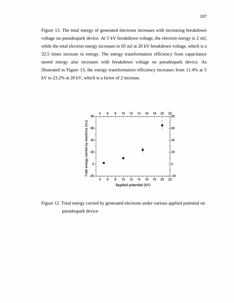
107
Figure 13. The total energy of generated electrons increases with increasing breakdown
voltage on pseudospark device. At 5 kV breakdown voltage, the electron energy is 2 mJ,
while the total electron energy increases to 65 mJ at 20 kV breakdown voltage, which is a
32.5 times increase in energy. The energy transformation efficiency from capacitance
stored energy also increases with breakdown voltage on pseudospark device. As
illustrated in Figure 13, the energy transformation efficiency increases from 11.4% at 5
kV to 23.2% at 20 kV, which is a factor of 2 increase.
Figure 12. Total energy carried by generated electrons under various applied potential on
pseudospark device

108
Figure 13. Energy transformation efficiency under various applied potential on
pseudospark device
4. DISCUSSION AND CONCLUSION
In this paper, an improved RPEA is used to analyze pulsed electron beam energy
from a multi-gap pseudospark discharge device. The presented RPEA is capable of
operating under tens of mTorr and holding 20 kV retarding potential without any leakage
breakdown on the RPEA. The time response of the presented RPEA setup is 8.3 ns. And
the low-resistance of the electron beam detector permits the collection of electron energy
at both high energy and low energy ranges. Experimental results on time-resolved
electron energy distributions by this RPEA setup under various breakdown voltage on
pseudospark device as electron beam source are presented in this work. Time-resolved
energy spectrum and particle numbers of electrons at various energy groups are
constructed through the differential electron beam pulses obtained at different retarding
potential. The evaluation of electron beam energy transformation efficiency is defined
and calculated compared to the input energy stored in the capacitors in pseudospark
device. Based on the results presented in previous sections, main conclusions are
summarized as follows:

109
1) The time-resolved electron energy spectrum shows that compared with the high
energy electrons which are emitted at the earliest phase of electron beam pulse within
approximately 300 ns after the ignition of gas breakdown in pseudospark device, the low
energy electrons are distributed more uniformly at the total time duration of the beam
pulse. For example, under 10 kV breakdown voltage on pseudospark device, the FWHM
of electrons temporal distribution spread for electrons at 2 keV is 800 ns, which is 4 times
the FWHM of electrons temporal distribution spread for electrons at 10 keV. Meanwhile,
the long “tail” of the electron beam pulse consists of mainly the low energy electrons.
Such observations and results are consistent with the results and simulations presented in
[9-10, 35]. In [9-10], the high energy and low energy electrons are distinguished by a
‘low-resistance’ Faraday cup and a ‘high-resistance’ Faraday cup. The electron beam
pulse collected by the high-resistance Faraday cup shows a narrow peak without the long
tail collected by the low-resistance Faraday cup. This difference illustrates that the low
energy electrons, rejected by the self-biased potential on high-resistance Faraday cup, is
mainly focused on the tail of electron beam pulse. In [35], the simulation results based on
a hybrid fluid-particle model show that the electrons accelerated to the full potential in
the cathode fall are emitted at the earliest phase of the beam pulse. The collision rate and
energy loss of electrons at high energy and low energy in vacuum and neutral gas is also
an important factor of the time-resolved electron distribution spread formation [36]. The
higher cross sections of low energy electrons cause a more dispersive distribution on the
full time duration of the electron beam pulse, while the lower cross section and collision
rate of high energy electrons result in a more concentrated distribution and propagation in
the neutral gas and vacuum.
2) All the generated electrons from pseudospark device are divided into separate
energy groups of 0-20%, 20%-40%, 40%-60%, 60%-80%, 80%-100% of full applied
breakdown potential under all the investigated breakdown voltages and the percentage of
electron numbers within individual energy groups is compared to the total generated
electrons for different breakdown voltages. The results show that under all the
investigated breakdown voltages, the electrons with maximum particle numbers are
located in the medium energy range, 40-60% of full applied potential. Furthermore, the
electron numbers at highest energy group are decreased with the breakdown voltage on

110
pseudospark discharge. Compared with the simulation results presented in [35], this
observation in our work suggests that under higher breakdown voltage, the electron
multiplication in the hollow cathode region is enhanced by higher cathode fall, causing
more high energy electrons generated at the earliest phase of electron emission process.
The electron particle numbers at lowest energy group below 20% of full applied potential
is also decreased with lower breakdown voltage. The formation of those low energy
electrons are still not well understood yet. Based on the statement suggested by Hartmann
and Gundersen [3,37], when the cathode sheath thickness is smaller than ,
field-emission or field-enhance thermionic emission becomes the dominating process for
the final discharge enhancement and electron multiplication and emission from cathode
in pseudospark device. Thus under higher breakdown voltage on pseudospark device, the
higher electric field strength compresses the cathode sheath thickness in the final process
of discharge and electron generation, which enhances more low energy electrons emitted
from pseudospark device. However, based on our results, the percentage of medium
energy electrons within 40%-60% is increased with lower breakdown voltage. The
formation of electrons within this energy range is still not well determined.
3) The energy transformation efficiency of electron generation is an important
performance indicator for an electron beam source. In our work, the energy
transformation efficiency of electron generation is defined as the ratio of total energy
carried by the electrons calculated from time-resolved energy spectrum, to the total input
energy, defined as the energy stored in the capacitors for pseudospark discharge. Previous
work on this topic is limited and only [38] presents a method to estimate the electron
beam generation efficiency. The total energy carried by electrons calculated from
time-resolved energy spectrum is increased from 2 mJ at 5 kV breakdown voltage to 65
mJ at 20 kV breakdown voltage. Compared with the results presented in [38] (20% of
efficiency of electron-beam generation by the pseudospark with external capacitor of 380
pF ), the energy transformation efficiency of electron generation by the pseudospark
device presented in this work is varied from 11.4%-23.2%, which is found to be
increased with breakdown voltage applied on pseudospark device with 1.4 nF external
capacitors.

111
REFERENCES
[1] Schaefer, G., Kristiansen, M. and Guenther, A. (eds) 1990 Gas Discharge
Closing Switches (New York, N.Y.: Plenum Press)
[2] Frank, K., Christiansen, J., “Fundamentals of the pseudospark and its
applications”, (1989) IEEE Transactions on Plasma Science, 17 (5), pp. 748-753.
[3] Gundersen M.A. and Schaerfer G., (eds) 1990 Physics and Applications of
Pseudosparks (New York, N.Y.: Plenum Press)
[4] Krasik, Ya.E., Gleizer, S., Chirko, K., Gleizer, J.Z., Felsteiner, J., Bernshtam, V.,
Matacotta, F.C., “Characterization of a channel spark discharge and the generated
electron beam” (2006) Journal of Applied Physics, 99 (6), art. no. 063303
[5] Witke, T., Lenk, A., Siemroth, P., “Channel spark discharges for thin film
technology” (1997) IEEE Transactions on Plasma Science, 25 (4), pp. 758-762.
[6] Dewald, E., Frank, K., Hoffmann, D.H.H., Tauschwitz, A., “Plasma development
in the low-pressure channel spark for pulsed intense electron beam generation”
(2002) IEEE Transactions on Plasma Science, 30 (1 III), pp. 363-374.
[7] Wyndham, E., Aliaga-Rossel, R., Chuaqui, H., Favre, M., Mitchell, I.H., Choi, P.,
“X-ray and plasma dynamics of an intermediate size capillary discharge” (2002)
IEEE Transactions on Plasma Science, 30 (1 III), pp. 401-407.
[8] Wyndham, E., Favre, M., Aliaga-Rossel, R., Chuaqui, H., Mitchell, I., Choi, P.,
“Formation and dynamics of a Z pinch in a high current capillary discharge in
initial vacuum” (2003) Journal of Applied Physics, 94 (9), pp. 5537-5542.
[9] Dewald, E., Frank, K., Hoffmann, D.H.H., Stark, R., Ganciu, M., Mandache,
B.N., Nistor, M.G., Pointu, A.-M., Popescu, I.-I., “Pulsed intense electron beams
generated in transient hollow cathode discharges: fundamentals and applications”
(1997) IEEE Transactions on Plasma Science, 25 (2), pp. 272-278.
[10] Dewald, E., Frank, K., Hoffmann, D.H.H., Tauschwitz, A., “Comparative studies
on intense electron beams generated in transient hollow-cathode discharges”
(2002) IEEE Transactions on Plasma Science, 30 (5 I), pp. 1820-1826.
[11] Rosier, O., Apetz, R., Bergmann, K., Jonkers, J., Wester, R., Neff, W., Pankert, J.,
“Frequency scaling in a hollow-cathode-triggered pinch plasma as radiation
source in the extreme ultraviolet” (2004) IEEE Transactions on Plasma Science,
32 (1 II), pp. 240-246.

112
[12] Boggasch, E., Rhee, M.J., “High-brightness pseudospark-produced electron beam”
(1990) Applied Physics Letters, 56 (18), pp. 1746-1748.
[13] Jain, K.K., Boggasch, E., Reiser, M., Rhee, M.J., “Experimental investigation of
a pseudospark-produced high-brightness electron beam” (1990) Physics of Fluids
B, 2 (10), pp. 2487-2491.
[14] Korolev, Y.D., Frank, K., “Discharge formation processes and glow-to-arc
transition in pseudospark switch” (1999) IEEE Transactions on Plasma Science,
27 (5), pp. 1525-1537.
[15] Bochkov, V.D., Dyagilev, V.M., Ushich, V.G., Frants, O.B., Korolev, Yu.D.,
Shemyakin, I.A., Frank, K., “Sealed-off pseudospark switches for pulsed power
applications (current status and prospects)” (2001) IEEE Transactions on Plasma
Science, 29 (5 I), pp. 802-808.
[16] Jiang, C., Kuthi, A., Gundersen, M.A., “Toward ultracompact pseudospark
switches” (2005) Applied Physics Letters, 86 (2), art. no. 024105, pp.
024105-1-024105-3.
[17] Bergmann, K., Lebert, R., Kiefer, J., Neff, W., “Triggering a radial multichannel
pseudospark switch using electrons emitted from material with high dielectric
constant” (1997) Applied Physics Letters, 71 (14), pp. 1936-1938.
[18] Yin, H., Cross, A.W., He, W., Phelps, A.D.R., Ronald, K., “Pseudospark
experiments: Cherenkov interaction and electron beam post-acceleration,” (2004)
IEEE Transactions on Plasma Science, 31 (1), pp. 233- 239.
[19] Yin, H., Cross, A.W., He, W., Phelps, A.D.R., Ronald, K., Bowes, D., Robertson,
C.W., “Millimeter wave generation from a pseudospark-sourced electron beam”
(2009) Physics of Plasmas, 16 (6), art. no. 063105.
[20] Yin, H., Robb, G.R.M., He, W., Phelps, A.D.R., Cross, A.W., Ronald, K.,
“Pseudospark-based electron beam and Cherenkov maser experiments” (2000)
Physics of Plasmas, 7 (12), pp. 5195-5205.
[21] Muntz, E.P., Kunc, J.A., Erwin, D.A., “A pulsed electron-photon fluoresence
technique for temperature and specie concentration measurement at points in
relatively dense, unseeded air flows” (1987) AIAA-87-1526. AIAA Thermophysics
Conference, 22 nd, Honolulu, Hawaii.
[22] Lufty, F.M., Muntz, E.P., “Initial experimental study of pulsed electron beam
fluorescence”, (1996) AIAA Journal, Vol. 34, No. 3, pp. 478-482.

113
[23] Macheret, S. O., Shneider, M. N., Miles, R. B., “Modeling of air plasma
generation by electron beams and high-voltage pulses,” (2000) AIAA-2000-2569,
AIAA Plasmadynamics and Lasers Conference, 31st, Denver, CO.
[24] Macheret, S. O., Miles, R. B., Nelson, G. L., Macheret, S. O., Miles, . B., Nelson,
G. L., “Feasibility study of a hybrid MHD/radiatively driven facility for
hypersonic ground testing,” (1997) AIAA-1997-2429, AIAA Plasmadynamics and
Lasers Conference, 28th, Atlanta, GA.
[25] Macheret, S. O., Shneider, M. N., Miles, R. B., “Electron beam generated
plasmas in hypersonic MHD channels,” (1999) AIAA-1999-3635, AIAA
Thermophysics Conference, 33rd, Norfolk, VA.
[26] Macheret, S. O., Shneider, M. N., Miles, R. B., Lipinski, R. J.,
“Electron-Beam-Generated Plasmas in Hypersonic Magnetohydrodynamic
Channels,” (2001) AIAA Journal, 0001-1452, Vol. 39, No. 6, pp 1127-1138.
[27] Ramaswamy, K., Destler, W.W., Rodgers, J., “A high-voltage triggered
pseudospark discharge experiment” (1996) Journal of Applied Physics, 80 (9), pp.
4887-4895.
[28] Lieberman, M.A., Lichtenber, A.J., 1994 Principles of plasma discharges and
materials processing (New York, N. Y.: Wiley)
[29] Jiang, C., Kuthi, A., Gundersen, M.A., Hartmann, W., “Pseudospark electron
beam as an excitation source for extreme ultraviolet generation” (2005) Applied
Physics Letters, 87 (13), art. no. 131501, pp. 1-3.
[30] Ding, B.N., Myers, T.J., Rhee, M.J., “Time-resolved energy spectrum of a
pseudospark-produced electron beam” (1993) Review of Scientific Instruments, 64
(6), pp. 1442-1444.
[31] Liu, C.J., Rhee, M.J., “Experimental study of post-acceleration and transport of a
pseudospark-produced electron beam” (1993) Proceedings of the IEEE Particle
Accelerator Conference, 1, pp. 688-690.
[32] Modreanu, G., Mandache, N.B., Pointu, A.M., Ganciu, M., Popescu, I.I.,
“Time-resolved measurement of the energy distribution function of an electron
beam created by a transient hollow cathode discharge”, (2000) Journal of Physics
D: Applied Physics, 33 (7), pp. 819-825.
[33] Hu, J., Rovey, J.L., “Faraday cup with nanosecond response and adjustable
impedance for fast electron beam characterization” (2011) Review of Scientific
Instruments, 82 (7), art. no. 073504.

114
[34] Zou, Y., Cui, Y., Haber, I., Reiser, M., O'Shea, P.G., “Longitudinal space-charge
effects in a retarding field energy analyzer”, (2003) Physical Review Special
Topics - Accelerators and Beams, 6 (11), pp. 1-10.
[35] Boeuf, Jean-Pierre, Pitchford, Leanne C., “Pseudospark discharges via computer
simulation” (1991) IEEE Transactions on Plasma Science, 19 (2), pp. 286-296.
[36] Miller, R.B., 1982 An introduction to the physics of intense charged particle
beams (New York, N.Y.: Plenum Press)
[37] Hartmann, W., Gundersen, M.A., “Origin of anomalous emission in superdense
glow discharge”, (1988) Physical Review Letters, 60 (23), pp. 2371-2374.
[38] Jain, K.K., Boggasch, E., Reiser, M., Rhee, M.J., “Experimental investigation of
a pseudospark-produced high-brightness electron beam” (1990) Physics of Fluids
B, 2 (10), pp. 2487-2491.

115
4. SUMMARY AND RECOMMENDATIONS FOR FUTURE WORK
The main emphasis of this dissertation is the experimental investigation of the
pseudospark discharge properties and intense electron beams generated by pseudospark
device. This dissertation consists of introduction of pseudospark discharge, literature
reviews of previous research work and application interest on pseudospark in a variety of
areas in chapter 1, introduction of the design and construction of a high voltage
pseudospark discharge experiment setup and diagnostic system in chapter 2, and three
journal articles which have been published or under review presented in chapter 3. Based
on research work completed in this dissertation, the following issues are recommended
for future work.
4.1 TRIGGER SOURCE IN THE HOLLOW CATHODE REGION
Pseudospark discharge can be operated under self-trigger mode, and external
trigger mode [1-4]. Trigger is an important issue in low pressure discharge, since in the
low pressure pulsed discharge of high E/N, the gas density is comparatively low to
1013
-1014
/cm3. At such low gas density, the initial ionization which is originated in the
hollow cathode region may be random in some cases. In many previous research work, it
has been shown that the introduction of trigger source in hollow cathode region can
improve the performance of stable operation in given pseudospark device [5-7]. The
trigger methods of pseudospark discharge includes optical trigger [5], high voltage pulse
trigger [6], and surface discharge over insulators [7].
In addition to the improvement of device performance, the introduction of trigger
can provide more accurate time-resolved information of development and process of
pseudospark discharge, which is of great importance for the fundamental gas discharge
physics. Electron beam generation by pseudospark discharge is also dependent on the
stable ionization counts originated in hollow cathode region [2]. Thus the introduction of
trigger source in hollow cathode also may improve the stable production of electron
beams from pseudospark device. The trigger mechanism and efficient trigger method for
the pseudospark device in this work are recommended for future work.

116
4.2 MODELING AND SIMULATION OF INTENSE PULSED ELECTRON
BEAMS INTERACTING WITH NEUTRAL GAS
As discussed in Chapter 1, the intense pulsed electron beam generated from
pseudospark has a variety of applications or potential applications in different areas. The
experimental investigations results completed in this dissertation have focused on
determinations of discharge properties and electron beam characteristics. But more
information can not be obtained by experimental work currently, thus the modeling and
particle simulations are required for assistance with experimental investigations and
multiple applications. An example is the plasma generation by intense pulsed electron
beam interacting with neutral gas [8-12]. The capacity of pulsed energetic electron beams
to generate plasma is of great research interest for many applications, while the
experimental investigations on this issue is very limited and challenging [12]. Thus the
theoretical modeling and simulations on the interaction of neutral gas with intense
energetic electrons is necessary [8-11]. XOOPIC, an X11 based Object Oriented
Particle-In-Cell code, can be applied to simulate such processes. The accurate
determination of time structure and electron energy distribution spectrum completed in
this dissertation provides necessary input information for the simulation work, which can
greatly improve the accuracy of simulation work. Thus the modeling of development of
intense pulsed electron beams interacting with neutral gas, and the ionization process by
energetic electrons with neutral gas under various pressures by XOOPIC is recommended
for future work and under progress currently.
4.3 OPERATIONS OF PSEUDOSPARK DISCHARGE UNDER HIGHER
VOLTAGES
In this dissertation, a high voltage pseudospark discharge experiment consisting
of high voltage charging and transmission, vacuum pumping, gas flow controller,
electron beam diagnostics is designed and constructed for high voltage operation. The
construction and calibration of high voltage operation and transmission system are

117
summarized in chapter 2. The presented experiment setup is operated under voltage up to
20 kV in this dissertation. The experiment results presented in this dissertation show that
the electron output, energy transformation efficiency and discharge properties are
improved with increasing applied voltage on pseudospark device. Thus the operation of
pseudospark discharge under higher applied voltages is recommended for future work to
improve the electron generation capacity of the device.

118
BIBLIOGRAPHY
[1] Gundersen M.A. and Schaerfer G., (eds) 1990 Physics and Applications of
Pseudosparks (New York, N.Y.: Plenum Press)
[2] Schaefer, G., Kristiansen, M. and Guenther, A. (eds) 1990 Gas Discharge
Closing Switches (New York, N.Y.: Plenum Press)
[3] Boeuf, Jean-Pierre, Pitchford, Leanne C., “Pseudospark discharges via computer
simulation”, (1991) IEEE Transactions on Plasma Science, 19 (2), pp. 286-296.
[4] Mehr, Thomas, Arenz, Hartmuth, Bickel, Peter, Christiansen, Jens, Frank, Klaus,
Goertler, Andreas, Heine, Frank, Hofmann, Detlef, Kowalewicz, Roland, Schlaug,
Martin, Tkotz, Rupert, “Trigger devices for pseudospark switches”, (1995) IEEE
Transactions on Plasma Science, 23 (3), pp. 324-329.
[5] Jiang, C., Kuthi, A., Gundersen, M.A. “Toward ultracompact pseudospark
switches”, (2005) Applied Physics Letters, Vol. 86, No. 2, art. no. 024105, pp.
024105-1-024105-3.
[6] Jain, K.K., Ding, B.N., Rhee, M.J., “Scaling study of pseudospark produced
electron beam”, (1991) Conference Record of the Particle Accelerator
Conference, Accelerator Science and Technology., IEEE, Vol. 3, pp.1972-1974.
[7] Goertler, Andreas, Christiansen, Jens, Dotzer, Robert, Frank, Klaus,
“Investigations of pulsed surface flashovers for the triggering of pseudospark
high-power switches”, (1989) IEEE Transactions on Plasma Science, 17 (5), pp.
762-765.
[8] Macheret, S. O., Shneider, M. N., Miles, R. B., and Lipinski, R. J.,
“Electron-Beam-Generated Plasmas in Hypersonic Magnetohydrodynamic
Channels”, (2001) AIAA Journal, 0001-1452, Vol. 39, No. 6, pp 1127-1138.
[9] Macheret, S. O., Miles, . B., Nelson, G. L., “Feasibility study of a hybrid
MHD/radiatively driven facility for hypersonic ground testing”, (1997)
AIAA-1997-2429, Plasmadynamics and Lasers Conference, 28th, Atlanta, GA.
[10] Macheret, S. O., Shneider, M. N., Miles, R. B., “Modeling of air plasma
generation by electron beams and high-voltage pulses”, (2000) AIAA-2000-2569,
AIAA Plasmadynamics and Lasers Conference, 31st, Denver, CO.
[11] Macheret, S. O., Shneider, M. N., Miles, R. B., “Electron beam generated
plasmas in hypersonic MHD channels”, (1999) AIAA-1999-3635, AIAA
Thermophysics Conference, 33rd, Norfolk, VA.

119
[12] Vidmar, R. J., Seeley, M. V., Serdyuchenko, A., Stalder, K. R., “Electrical, RF,
and optical diagnostics in E-beam excited air plasma”, (2008) AIAA 2008-1111,
AIAA Aerospace Sciences Meeting and Exhibit, 46th, Reno, NV.

120
VITA
Jing Hu was born in Hubei, China. She received her Bachelor of Engineering
degree in Electrical Engineering in 2004 from Xi’an Institute of Telecommunications,
Xi’an, China. In 2007, she received her Master of Science degree in Atomic and
Molecular Physics from Chinese Academy of Sciences, China. She joined the Ph.D
degree program in Aerospace Engineering at Missouri University of Science and
Technology in Rolla, Missouri in Fall semester, 2008. And she received her Doctor of
Philosophy in Aerospace Engineering from Missouri University of Science and
Technology in December 2012. Her research interests include high voltage pulse power
technology, gas discharge physics, fast signal measurements, and charge particle
diagnostics.


![Capillary Extraction of the Ionic Liquid [Bmim][DCA] for ...eplab.ae.illinois.edu/Publications/AIAA-2012-3738.pdf · Figure 2. is a schematic diagram of the used for the experimental](https://img.pdfslide.us/doc/110x75/5f30bafcf93ef7490870592b/capillary-extraction-of-the-ionic-liquid-bmimdca-for-eplabae-figure-2.jpg)