Embed Size (px)
Citation preview
0733-8724 (c) 2016 IEEE. Personal use is permitted, but republication/redistribution requires IEEE permission. See http://www.ieee.org/publications_standards/publications/rights/index.html for more information.
This article has been accepted for publication in a future issue of this journal, but has not been fully edited. Content may change prior to final publication. Citation information: DOI 10.1109/JLT.2016.2608801, Journal ofLightwave Technology
> REPLACE THIS LINE WITH YOUR PAPER IDENTIFICATION NUMBER (DOUBLE-CLICK HERE TO EDIT) <
1
Abstract— Directive optical leaky wave antennas (OLWAs)
fabricated in CMOS-compatible semiconductor planar waveguide
technology have the potential to provide high directivity with
electrical tunability promising for modulation and switching
capabilities. We experimentally demonstrate directive radiation
from a silicon nitride (Si3N4) waveguide-based OLWA. The
OLWA design comprises a crystalline silicon (Si) nanowire array
buried inside a Si3N4 waveguide. Each Si nanowire has a width of
260 nm and a height of 150 nm. The OLWA is designed to exhibit a
directive radiation pattern at telecom wavelengths. The measured
radiation pattern at the wavelength 1550 nm has its maximum
emission intensity at the angle of 85.1° relative to the waveguide
axis and a half-power beam width of approximately 5.0°, which
are consistent with our theoretical predictions. The results indicate
that the TM mode is more radiative than the TE mode in our
fabricated devices. Also, the radiation pattern of the measured
OLWA shows dependence on wavelength, which is typical of leaky
wave antennas. The device is promising in chip-to-space optical
interconnect applications.
Index Terms— Directive antennas, leaky wave antennas, optical
antennas, gratings, silicon nitride.
I. INTRODUCTION
eaky wave antennas are a class of antennas that use
travelling waves to produce narrow radiated beams [1]. The
theory and applications of leaky waves (LWs) have been
extensively developed since the first known LW antenna
introduced by W.W. Hansen in 1940 [2]. A fundamental method
of achieving LW radiation is to use waveguides with periodic
features, which consists of a waveguide supporting a slow
(guided) wave that has been periodically modulated along the
waveguide axis. The periodic modulations create an infinite
number of Floquet harmonics, among which one Floquet
harmonic will be a fast wave and thus can be leaked as a
radiating wave [3], [4]. The LW antennas have the advantage of
radiating in either forward or backward directions, as its beam
will scan a range of angles by changing frequency. Many LW
antennas, including corrugated metal films [5]–[9] and
plasmonic nanosphere arrays [10]–[12], utilize periodic
structures to enhance radiation in optical frequencies. Besides
metallic structures, dielectric-based periodic antennas have also
been widely used in millimeter wave [13] and optical
applications [14].
Optical leaky wave antennas (OLWAs) can direct light, focus
energy, and enhance light-matter interaction. Therefore, they
are promising for applications such as free space optical
communications [15], space-division multiplexing [16], [17],
and tunable grating couplers [18], [19]. We have recently
introduced the theory of CMOS compatible OLWAs [20]–[22]
that provides directive radiation at 1550 nm in a dielectric
waveguide comprising periodic semiconductor perturbations.
Readers may refer to our previous work [20]–[24] for further
information on the theoretical design and preliminary
investigations on its modulation capability. The device is
designed on a silicon nitride (Si3N4) on silicon-on-insulator
(SOI) platform that has drawn tremendous interest as a
promising solution to integrated optical interconnections in
recent years [25]–[27]. Silicon nitride is chosen as the dielectric
waveguide material due to its low propagation loss, wide
transparent window and silicon-compatible fabrication
technology [28]. The SOI platform, which reached a mature
stage for integrated silicon photonics, is chosen to build the
silicon nanowires. SOI has been widely used to deliver
chip-scale passive photonic devices, imaging devices [29], and
nonlinear devices [30] with CMOS fabrication compatibility
[31]. The aforementioned very slowly attenuating LW is
realized by designing the silicon nanowires buried inside the
Si3N4 waveguide with a small filing factor. The electrical
control capability of the proposed OLWA can be achieved by
engineering the optical parameters of Si via plasma dispersion
effect [32], [33] or Franz-Keldysh effect [34].
In this paper, we present the experimental demonstration of a
CMOS-compatible OLWA made of a dielectric waveguide and
semiconductor perturbations. The OLWA radiation pattern is
characterized in the altitude angle θ ranging from 65° to 112°
with a radiation peak occurring at 85.1° and a half-power beam
width of 5.0° at 1550 nm wavelength. The main beam is well
resolved in the experiments together with the
frequency-dependent far-field scanning. All side lobes are at
least -7 dB below the main lobe, indicating a directive emission.
This is the first demonstration of embedding silicon wires as
perturbations in a dielectric waveguide in a CMOS compatible
fabrication manner. The incorporation of semiconductor
enables electrical control on the radiation, which can be utilized
Experimental Demonstration of Directive Si3N4
Optical Leaky Wave Antennas with
Semiconductor Perturbations
Qiancheng Zhao, Student Member, IEEE, Caner Guclu, Student Member, IEEE, Yuewang Huang,
Filippo Capolino, Senior Member, IEEE, and Ozdal Boyraz, Senior Member, IEEE
L
0733-8724 (c) 2016 IEEE. Personal use is permitted, but republication/redistribution requires IEEE permission. See http://www.ieee.org/publications_standards/publications/rights/index.html for more information.
This article has been accepted for publication in a future issue of this journal, but has not been fully edited. Content may change prior to final publication. Citation information: DOI 10.1109/JLT.2016.2608801, Journal ofLightwave Technology
> REPLACE THIS LINE WITH YOUR PAPER IDENTIFICATION NUMBER (DOUBLE-CLICK HERE TO EDIT) <
2
in chip-to-space communications [35].
This paper is organized as follows. Section II briefly
introduces the LW principles. Section III includes the OLWA
fabrication procedure, experiment setup, and testing results.
The radiation pattern is examined to reveal its
wavelength-dependence and polarization-dependence. A
numerical simulation is also included for verification. In Section
IV, we summarize the performance of the OLWA and discuss its
potential applications.
II. THEORETICAL ANALYSIS
Periodic Si
perturbations
x
yz
Fig. 1. Schematic of the OLWA made of a Si3N4 waveguide over periodic Si
perturbations for possible electronic control.
The geometry of the radiating structure under study is shown
in Fig. 1. The OLWA consists of a Si3N4 waveguide with buried
Si perturbations on an SOI platform. The slow wave guided by
the Si3N4 waveguide becomes leaky due to the periodic Si
perturbations. The overall leaky mode that propagates in the
waveguide can be represented as a superposition of an infinite
set of Floquet spatial harmonics travelling with wave numbers
kz,n = βz,n + iαz [22], where βz,n = βz,0 + 2πn/d and z is assumed to
be the direction of propagation.. Here, n is an integer from -∞ to
+∞ that tags the n-th spatial harmonic, βz,0 is the fundamental
harmonic’s phase constant, and d is the period of the
perturbations. All spatial harmonics have the same attenuation
constant αz [9], [20], [22] among which, one of them is
engineered to be a fast wave that leads to the LW radiation.
Usually this fast harmonic is the n = -1 harmonic, and
thus , 1 ,0 2 /z z d such that , 1z hk , with hk the
wavenumber in the host medium. The leaky harmonic’s electric
field propagates as
, 11, , , z z
i z zx y z x y e e
E E (1)
along the perturbed section of the waveguide. It is important to
stress that the leaky wave is not bounded to the waveguide. On a
radiation aperture chosen sufficiently above and outside the
waveguide, the field can be assumed as only composed of -1
harmonic, since all other harmonics have their field
distributions strictly confined in the waveguide core.
The radiated beam from such an antenna can be modeled by
using equivalent aperture integration technique, in which most
of the radiation is directed to 0 where 0 is determined by
the expression 0 , 1cos /z hk [20]. We have used the
information that the radiated beam is generated by the -1
harmonic. Therefore, the radiation close to the “broadside”
direction (e.g., the direction almost orthogonal to the waveguide
axis z) is obtained when , 1z hk . Values for the actual LW
antenna studied in this paper are given in Appendix. The
normalized far-field pattern on the y-z plane is derived as [20],
, 1
, 1
sin cos2
cos2
h z
h z
Lk k
FL
k k
(2)
where L is the length of the radiating aperture assumed equal to
the length of the OLWA. The leaky harmonic’s wave number
, 1zk can be extracted from the full-wave simulations by
sampling the field periodically along the perturbed waveguide,
and then the phase constant and the attenuation constant can be
recovered by fitting curves to the simulated field’s phase and
amplitude profile as shown in Ref. [20]. We stress that the
waveguide has two fundamental modes called TM and TE
modes which are respectively defined as (i) the vertically
electric field polarized mode which has perfect magnetic
conductor symmetry with respect to the y-z plane and (ii) the
horizontally electric field polarized mode which has perfect
electric conductor symmetry with respect to y-z plane. When the
waveguide is periodically perturbed, both of these modes may
lead to leaky-wave radiation whose far-field pattern can be
approximated by Eq. (2). It is elaborated in the following
section that only the TM mode radiation is observable in the
conducted experiment.
III. EXPERIMENTAL RESULTS
A. OLWA Fabrication
The OLWA is fabricated on an SOI wafer [36] with 1 μm
thick silicon dioxide (SiO2) buffer layer. The Si device layer, in
which the nanowires are patterned, is thinned to be 150 nm thick
by dry etching and coated with back anti-reflection coating
(BARC) layer and the photoresist. Lithography is implemented
via an ASML 5500 optical stepper, followed by fluorine RIE
plasma etching to transfer patterns from the photoresist to the Si
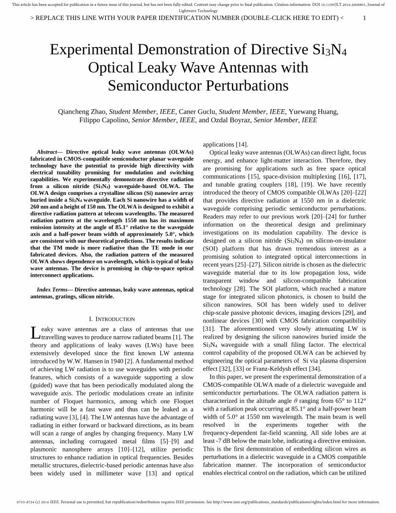
device layer. The fabricated Si nanowires are shown in Fig. 2(a).
The narrow vertical lines are the Si wires which are connected to
a Si “skeleton” to prevent the nanowires from being peeled off.
The array has 50 nanowires with a spatial periodicity d = 1 µm,
and each wire is measured to be 260 nm wide in the z direction.
The Si3N4 waveguides are then deposited by the low-pressure
chemical vapor deposition (LPCVD) method with a
stoichiometric recipe, and patterned by standard optical
lithography, followed by fluorine RIE etching. The fabricated
Si3N4 waveguide is shown in Fig. 2(b), extending horizontally in
the SEM image. The waveguide that is used in our experiments
is measured to be 1 µm wide (in the x direction) and 735 nm
0733-8724 (c) 2016 IEEE. Personal use is permitted, but republication/redistribution requires IEEE permission. See http://www.ieee.org/publications_standards/publications/rights/index.html for more information.
This article has been accepted for publication in a future issue of this journal, but has not been fully edited. Content may change prior to final publication. Citation information: DOI 10.1109/JLT.2016.2608801, Journal ofLightwave Technology
> REPLACE THIS LINE WITH YOUR PAPER IDENTIFICATION NUMBER (DOUBLE-CLICK HERE TO EDIT) <
3
thick (in the y direction). B. Measurement Setup and Procedure
Fig. 2. (a) Scanning electron microscopy (SEM) image of the fabricated Si perturbations. (b) SEM picture of the fabricated Si3N4 waveguide sitting on the periodic
Si perturbations.
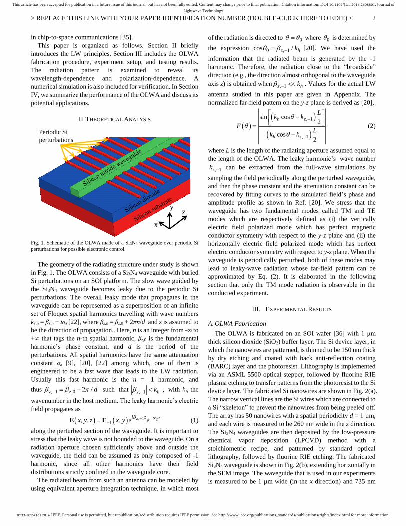
Fig. 3. (a) Schematic of the OLWA radiation pattern measurement setup. EDFA, TLF, and FP stand for erbium-doped fiber amplifier, tapered lens fiber, and fiber
probe, respectively. (b) Schematic of the various FP orientations during the measurement of radiated power at various angular directions. The angle between the
radiation detection direction and the waveguide propagation direction is denoted as θ.
The OLWA is designed to radiate in both upward and
downward directions off the wafer plane. The Si substrate
bottom surface is rough and difficult to detect experimentally.
Therefore, we only report the characterization of the radiation in
the upward direction. The experimental setup that is utilized in
the measurement of the far-field patterns is illustrated in Fig.
3(a). A tunable infrared laser (MLS-2100, Santec) is used as the
source, followed by an erbium-doped fiber amplifier (EDFA,
AEDFA-C-231-R, Amonics) to boost the power. To feed the
antenna, a tapered and lensed fiber (TLF, OZ Optics Ltd.) is
employed to butt-couple light into the waveguide facet. The
polarization of the light at the TLF is handled by the
polarization controller depicted in Fig. 3(a).
On the detection arm, a cleaved SM-28 fiber probe (FP) is used
to detect the radiation above the OLWA device. Due to the
single mode fiber’s small numerical aperture, the FP has a half
power beam width of approximately 3° and an antenna
directivity of 26 dB. It is a directive detector and thus must be
properly oriented. An angle controller is employed to adjust the
FP direction. An optical power meter (1830-C, Newport
Corporation) is employed to monitor the power collected by the
FP.
Before we start the measurement of radiation pattern, the FP is
oriented at a reference angle f (e.g. 85f that is close to
the expected maximum radiation angle) and we make sure it
points to the antenna by controlling its position along the z axis
to maximize the power reception for that fixed FP orientation.
Then the polarization controller preceding the TLF is adjusted
for maximizing the reception power at the FP, and this
polarization state is not altered during the radiation pattern
measurement.
The radiation intensity measurement at a certain angle θ starts
by first orienting the FP along θ. Next the FP is horizontally
scanned along the z axis by a mechanical stage via fine tuning
until the maximum power reception is achieved. In doing so, we
maintain a constant vertical distance of H = 510 μm between the
FP tip to the waveguide surface as shown in Fig. 3(b).
Maximum power reception occurs when the FP points to the
antenna since the FP is a directive detector. This maximum
power is recorded as probe ,P R which is the power received
at angle θ and at the distance / sinR H between the FP and
the OLWA radiation center. The steps above are repeated for
every angle θ reported in the radiation pattern. Since the
0733-8724 (c) 2016 IEEE. Personal use is permitted, but republication/redistribution requires IEEE permission. See http://www.ieee.org/publications_standards/publications/rights/index.html for more information.
This article has been accepted for publication in a future issue of this journal, but has not been fully edited. Content may change prior to final publication. Citation information: DOI 10.1109/JLT.2016.2608801, Journal ofLightwave Technology
> REPLACE THIS LINE WITH YOUR PAPER IDENTIFICATION NUMBER (DOUBLE-CLICK HERE TO EDIT) <
4
radiation intensity scales proportionally to 1/R2, the radiation
pattern P is then retrieved by
2
2probe probe 2
, ,sin
HP R P R P R
. (3)
During the radiation pattern measurement, the reception
power data are prone to temporal power drift due to the
mechanical instability of the translational stages. Each angular
sweep starts with 65 and ends with 110 in our
experiment. In order to compensate for power drift, the power
reception at 65 is measured twice, before and after the
angular sweep. The ratio of the power measured at 65
after the whole angular sweep over the power measured at
65 before the angular sweep is denoted as . This ratio
reflects the temporal power drift of the system. To compensate
the drift, the power measured at each angle is weighted by a
factor between 1 and 1 / by assuming that the drift is linear
with time, and assuming that the angle measurements are
separated by equal time intervals. It is worth noting that the
power drift did not bring the signal at the far field below the
noise level. It could be removed with better controlled stages.
The FP tip in our measurement setup is not in the far-field in
the strict sense, as a sacrifice to increase the dynamic range of
the power reception. The OLWA length is 50 μmD ,
accordingly the far field is at distances larger than 2
02 / 3225 μmD and the reactive near-field boundary is at
distances larger than 1/2
300.62 / 176 μmD [37]. Note
that the effective OLWA length (i.e., the length where most of
the radiation comes from owing to the exponential decay. It
could be defined as the effective aperture, but in one dimension)
is shorter than D. However, considering the whole OLWA
length D in the calculation lets us have a conservative estimation
of field boundaries. The measurement distance H = 510 µm falls
into the Fresnel region, i.e., in the radiating near-field region
[37], located between the reactive near field boundary and the
far field boundary. In Appendix, we prove that the quasi
far-field pattern collected at H = 510 μm height is quite close to
the accurate far field pattern.
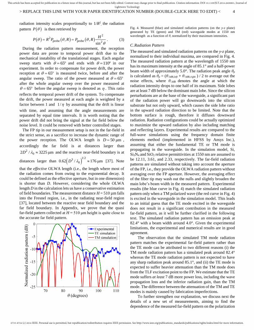
Fig. 4. Measured (blue) and simulated radiation patterns (on the y-z plane)
generated by TE (green) and TM (red) waveguide modes at 1550 nm
wavelength as a function of θ, normalized by their maximum intensities.
C. Radiation Pattern
The measured and simulated radiation patterns on the y-z plane,
normalized to their individual maxima, are compared in Fig. 4.
The measured radiation pattern at the wavelength of 1550 nm
has its maximum intensity at the angle of 85.1° and a half-power
beam width of approximately 5.0°. The radiation peak angle θp
is calculated as θp = (θ-3dB,left + θ-3dB,right ) / 2 to average out the
noise effects, where θ-3dB denotes the angle at which the
radiation intensity drops to one half of its maximum. Side lobes
are at least 7 dB below the dominant main lobe. Since the silicon
perturbations are at the base of the waveguide, a significant part
of the radiation power will go downwards into the silicon
substrate but not only upward, which causes the side lobe ratio
in the upward radiation direction to be limited. Note that the
bottom surface is rough, therefore it diffuses downward
radiation. Radiation configurations could be actually optimized
to maximize the upward radiation by also including matching
and reflecting layers. Experimental results are compared to the
full-wave simulations using the frequency domain finite
elements method (implemented in HFSS by Ansys Inc.),
assuming that either the fundamental TE or TM mode is
propagating in the waveguide. In the simulation model, Si,
Si3N4 and SiO2 relative permittivities at 1550 nm are assumed to
be 12.11, 3.61, and 2.33, respectively. The far-field radiation
patterns are simulated without taking into account the aperture
of the FP, i.e., they provide the OLWA radiation pattern without
averaging over the FP aperture. However, the averaging effect
of the fiber tip may wash out the nulls and slightly broaden the
main lobe’s beam width in the measured pattern. Experimental
results (the blue curve in Fig. 4) match the simulated radiation
pattern only when a TM polarized wave (the red curve in Fig. 4)
is excited in the waveguide in the simulation model. This leads
to an initial guess that the TE mode excited in the waveguide
does not result in a significant contribution in the measured
far-field pattern, as it will be further clarified in the following
text. The simulated radiation pattern has an emission peak at
82.4° with a beam width around 4.0°. Given the experimental
limitations, the experimental and numerical results are in good
agreement.
The observation that the simulated TM mode radiation
pattern matches the experimental far-field pattern rather than
the TE mode can be attributed to two different reasons (i) the
TM mode radiation pattern has a simulated peak around 82.4°
whereas the TE mode radiation pattern is not expected to have
any sharp radiation peak around 85.1°, and (ii) the TE mode is
expected to suffer heavier attenuation than the TM mode does
from the TLF excitation point to the FP. We estimate that the TE
mode suffers at least 7 dB more power loss, including the wave
propagation loss and the inferior radiation gain, than the TM
mode. The difference between the attenuation of the TM and TE
modes is mainly caused by fabrication imperfections.
To further strengthen our explanation, we discuss next the
details of a new set of measurements, aiming to find the
dependence of the measured far-field pattern on the polarization
0733-8724 (c) 2016 IEEE. Personal use is permitted, but republication/redistribution requires IEEE permission. See http://www.ieee.org/publications_standards/publications/rights/index.html for more information.
This article has been accepted for publication in a future issue of this journal, but has not been fully edited. Content may change prior to final publication. Citation information: DOI 10.1109/JLT.2016.2608801, Journal ofLightwave Technology
> REPLACE THIS LINE WITH YOUR PAPER IDENTIFICATION NUMBER (DOUBLE-CLICK HERE TO EDIT) <
5
of the wave launched at the TLF [Fig. 3(a)]. Due to the
experimental limitations, we can use only the measured far-field
signature to identify the polarization of the mode in the OLWA.
We carry out two sets of far-field pattern measurements
corresponding to two extreme states of the polarizations: (i) first
the polarization of the launched field is varied via the
polarization controller [Fig. 3(a)] to maximize the power
reception at the reference angle ,1 85f and then the
radiation pattern is measured as explained in Sec. III-B without
altering this polarization state, namely MaxP state; (ii) again at
the same reference angle ,1 85f , the polarization of the
wave at the TLF is varied to minimize the power reception and
the radiation pattern is measured again for this polarization
state, namely MinP state. We then repeat steps (i) and (ii)
starting with two other reference angles ,2 75f and
,3 65f . The motivation of using multiple reference angles
arises from the fact that the TM mode may radiate more power
than the TE mode at one radiation angle, but it may have less
power than TE mode radiation at another angle, as illustrated in
Fig. 4. This is also the reason that the polarization state should
be tuned at first and then stay intact while sweeping the angle.
By changing the reference angle, the polarization state
corresponding to MaxP and MinP will change, so that we catch
the far-field signature of distinct waveguide modes that may
radiate.
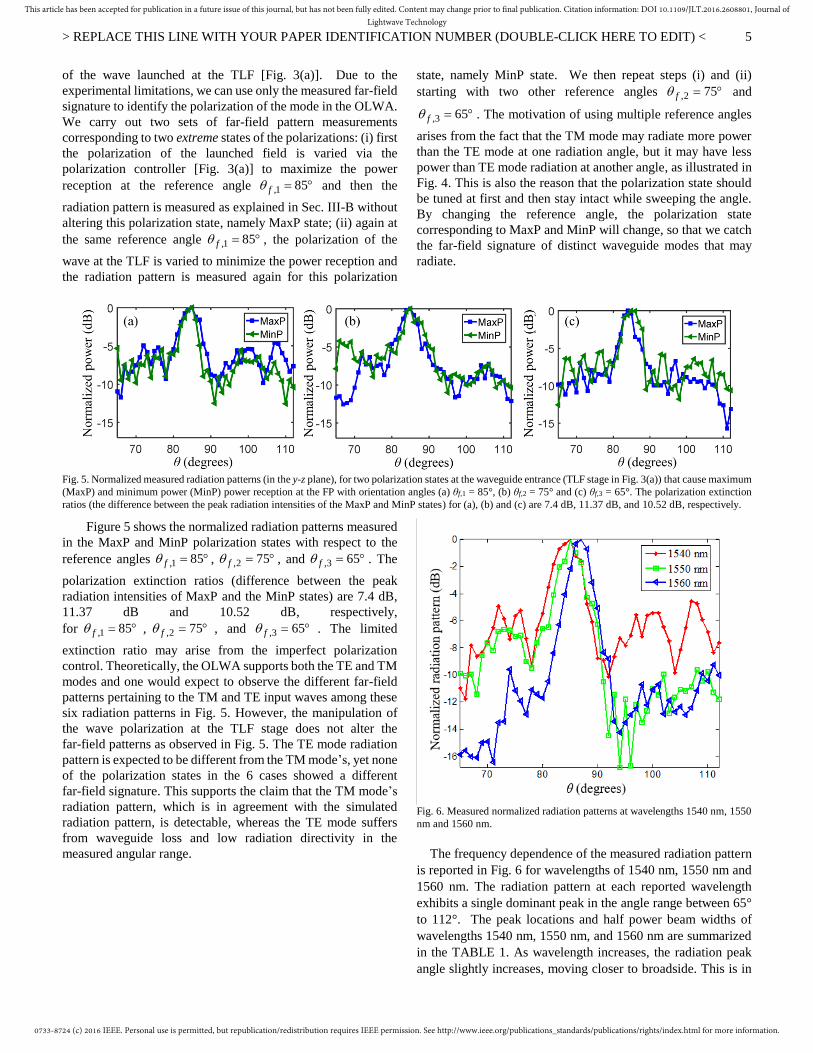
Fig. 5. Normalized measured radiation patterns (in the y-z plane), for two polarization states at the waveguide entrance (TLF stage in Fig. 3(a)) that cause maximum
(MaxP) and minimum power (MinP) power reception at the FP with orientation angles (a) θf,1 = 85°, (b) θf,2 = 75° and (c) θf,3 = 65°. The polarization extinction
ratios (the difference between the peak radiation intensities of the MaxP and MinP states) for (a), (b) and (c) are 7.4 dB, 11.37 dB, and 10.52 dB, respectively.
Figure 5 shows the normalized radiation patterns measured
in the MaxP and MinP polarization states with respect to the
reference angles ,1 85f , ,2 75f , and ,3 65f . The
polarization extinction ratios (difference between the peak
radiation intensities of MaxP and the MinP states) are 7.4 dB,
11.37 dB and 10.52 dB, respectively,
for ,1 85f , ,2 75f , and ,3 65f . The limited
extinction ratio may arise from the imperfect polarization
control. Theoretically, the OLWA supports both the TE and TM
modes and one would expect to observe the different far-field
patterns pertaining to the TM and TE input waves among these
six radiation patterns in Fig. 5. However, the manipulation of
the wave polarization at the TLF stage does not alter the
far-field patterns as observed in Fig. 5. The TE mode radiation
pattern is expected to be different from the TM mode’s, yet none
of the polarization states in the 6 cases showed a different
far-field signature. This supports the claim that the TM mode’s
radiation pattern, which is in agreement with the simulated
radiation pattern, is detectable, whereas the TE mode suffers
from waveguide loss and low radiation directivity in the
measured angular range.
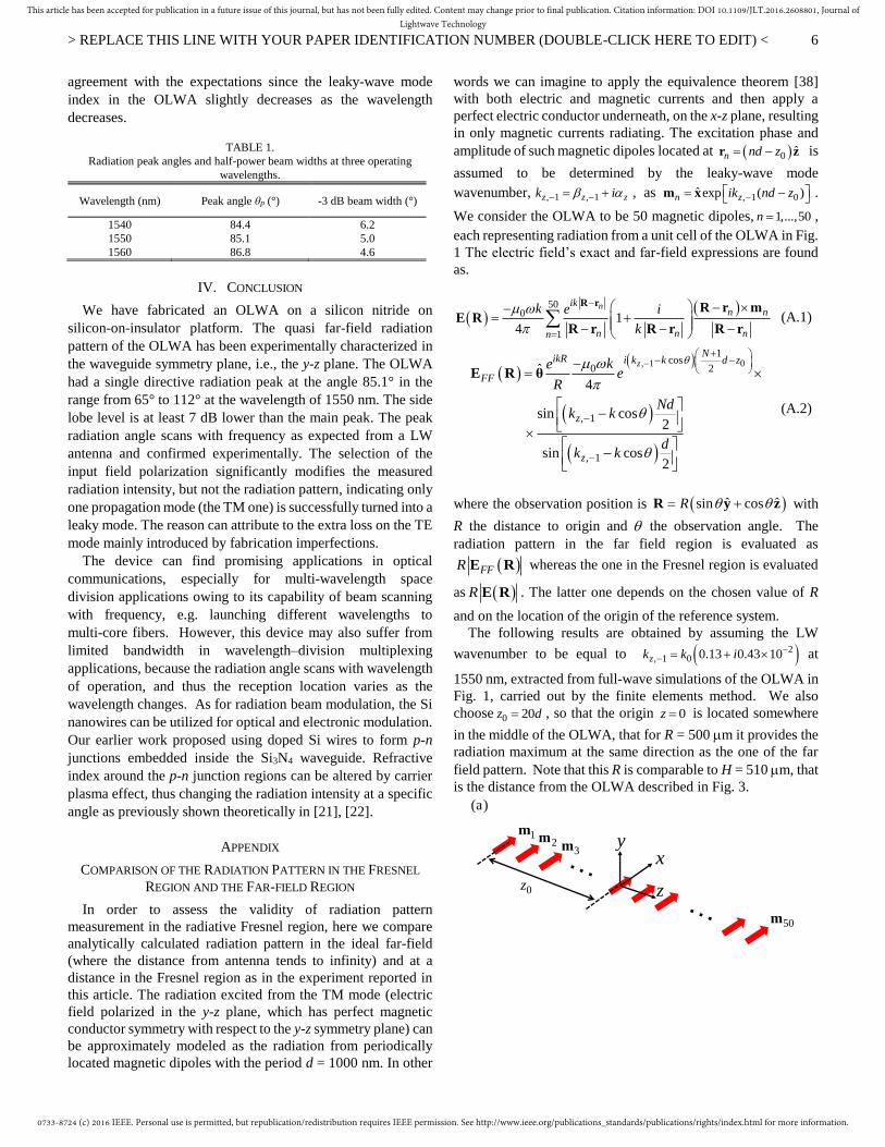
Fig. 6. Measured normalized radiation patterns at wavelengths 1540 nm, 1550
nm and 1560 nm.
The frequency dependence of the measured radiation pattern
is reported in Fig. 6 for wavelengths of 1540 nm, 1550 nm and
1560 nm. The radiation pattern at each reported wavelength
exhibits a single dominant peak in the angle range between 65°
to 112°. The peak locations and half power beam widths of
wavelengths 1540 nm, 1550 nm, and 1560 nm are summarized
in the TABLE 1. As wavelength increases, the radiation peak
angle slightly increases, moving closer to broadside. This is in
0733-8724 (c) 2016 IEEE. Personal use is permitted, but republication/redistribution requires IEEE permission. See http://www.ieee.org/publications_standards/publications/rights/index.html for more information.
This article has been accepted for publication in a future issue of this journal, but has not been fully edited. Content may change prior to final publication. Citation information: DOI 10.1109/JLT.2016.2608801, Journal ofLightwave Technology
> REPLACE THIS LINE WITH YOUR PAPER IDENTIFICATION NUMBER (DOUBLE-CLICK HERE TO EDIT) <
6
agreement with the expectations since the leaky-wave mode
index in the OLWA slightly decreases as the wavelength
decreases.
TABLE 1.
Radiation peak angles and half-power beam widths at three operating
wavelengths.
Wavelength (nm) Peak angle θp (°) -3 dB beam width (°)
1540 84.4 6.2
1550 85.1 5.0
1560 86.8 4.6
IV. CONCLUSION
We have fabricated an OLWA on a silicon nitride on
silicon-on-insulator platform. The quasi far-field radiation
pattern of the OLWA has been experimentally characterized in
the waveguide symmetry plane, i.e., the y-z plane. The OLWA
had a single directive radiation peak at the angle 85.1° in the
range from 65° to 112° at the wavelength of 1550 nm. The side
lobe level is at least 7 dB lower than the main peak. The peak
radiation angle scans with frequency as expected from a LW
antenna and confirmed experimentally. The selection of the
input field polarization significantly modifies the measured
radiation intensity, but not the radiation pattern, indicating only
one propagation mode (the TM one) is successfully turned into a
leaky mode. The reason can attribute to the extra loss on the TE
mode mainly introduced by fabrication imperfections.
The device can find promising applications in optical
communications, especially for multi-wavelength space
division applications owing to its capability of beam scanning
with frequency, e.g. launching different wavelengths to
multi-core fibers. However, this device may also suffer from
limited bandwidth in wavelength–division multiplexing
applications, because the radiation angle scans with wavelength
of operation, and thus the reception location varies as the
wavelength changes. As for radiation beam modulation, the Si
nanowires can be utilized for optical and electronic modulation.
Our earlier work proposed using doped Si wires to form p-n
junctions embedded inside the Si3N4 waveguide. Refractive
index around the p-n junction regions can be altered by carrier
plasma effect, thus changing the radiation intensity at a specific
angle as previously shown theoretically in [21], [22].
APPENDIX
COMPARISON OF THE RADIATION PATTERN IN THE FRESNEL
REGION AND THE FAR-FIELD REGION
In order to assess the validity of radiation pattern
measurement in the radiative Fresnel region, here we compare
analytically calculated radiation pattern in the ideal far-field
(where the distance from antenna tends to infinity) and at a
distance in the Fresnel region as in the experiment reported in
this article. The radiation excited from the TM mode (electric
field polarized in the y-z plane, which has perfect magnetic
conductor symmetry with respect to the y-z symmetry plane) can
be approximately modeled as the radiation from periodically
located magnetic dipoles with the period d = 1000 nm. In other
words we can imagine to apply the equivalence theorem [38]
with both electric and magnetic currents and then apply a
perfect electric conductor underneath, on the x-z plane, resulting
in only magnetic currents radiating. The excitation phase and
amplitude of such magnetic dipoles located at 0 ˆn nd z r z is
assumed to be determined by the leaky-wave mode
wavenumber, , 1 , 1z z zk i , as , 1 0ˆ exp ( )n zik nd z m x .
We consider the OLWA to be 50 magnetic dipoles, 1,...,50n ,
each representing radiation from a unit cell of the OLWA in Fig.
1 The electric field’s exact and far-field expressions are found
as.
50
0
1
14
nikn n
n n nn
k e i
k
R r R r m
E RR r R r R r
(A.1)
, 1 01
cos0 2
, 1
, 1
ˆ4
sin cos2
sin cos2
zN
ikR i k k d z
FF
z
z
kee
R
Ndk k
dk k
E R θ
(A.2)
where the observation position is ˆ ˆsin cosR R y z with
R the distance to origin and the observation angle. The
radiation pattern in the far field region is evaluated as
FFR E R whereas the one in the Fresnel region is evaluated
as R E R . The latter one depends on the chosen value of R
and on the location of the origin of the reference system.
The following results are obtained by assuming the LW
wavenumber to be equal to 2, 1 0 0.13 0.43 10zk k i at
1550 nm, extracted from full-wave simulations of the OLWA in
Fig. 1, carried out by the finite elements method. We also
choose 0 20z d , so that the origin 0z is located somewhere
in the middle of the OLWA, that for R = 500 m it provides the
radiation maximum at the same direction as the one of the far
field pattern. Note that this R is comparable to H = 510 m, that
is the distance from the OLWA described in Fig. 3.
z
yx
1m2m
3m
50m
(a)
0z
0733-8724 (c) 2016 IEEE. Personal use is permitted, but republication/redistribution requires IEEE permission. See http://www.ieee.org/publications_standards/publications/rights/index.html for more information.
This article has been accepted for publication in a future issue of this journal, but has not been fully edited. Content may change prior to final publication. Citation information: DOI 10.1109/JLT.2016.2608801, Journal ofLightwave Technology
> REPLACE THIS LINE WITH YOUR PAPER IDENTIFICATION NUMBER (DOUBLE-CLICK HERE TO EDIT) <
7
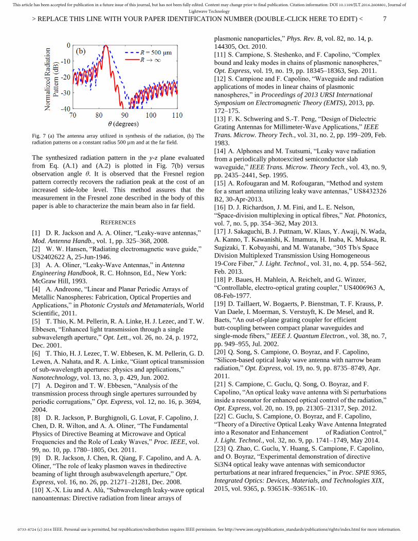
Fig. 7 (a) The antenna array utilized in synthesis of the radiation, (b) The
radiation patterns on a constant radius 500 µm and at the far field.
The synthesized radiation pattern in the y-z plane evaluated
from Eq. (A.1) and (A.2) is plotted in Fig. 7(b) versus
observation angle θ. It is observed that the Fresnel region
pattern correctly recovers the radiation peak at the cost of an
increased side-lobe level. This method assures that the
measurement in the Fresnel zone described in the body of this
paper is able to characterize the main beam also in far field.
REFERENCES
[1] D. R. Jackson and A. A. Oliner, “Leaky-wave antennas,”
Mod. Antenna Handb., vol. 1, pp. 325–368, 2008.
[2] W. W. Hansen, “Radiating electromagnetic wave guide,”
US2402622 A, 25-Jun-1946.
[3] A. A. Oliner, “Leaky-Wave Antennas,” in Antenna
Engineering Handbook, R. C. Hohnson, Ed., New York:
McGraw Hill, 1993.
[4] A. Andreone, “Linear and Planar Periodic Arrays of
Metallic Nanospheres: Fabrication, Optical Properties and
Applications,” in Photonic Crystals and Metamaterials, World
Scientific, 2011.
[5] T. Thio, K. M. Pellerin, R. A. Linke, H. J. Lezec, and T. W.
Ebbesen, “Enhanced light transmission through a single
subwavelength aperture,” Opt. Lett., vol. 26, no. 24, p. 1972,
Dec. 2001.
[6] T. Thio, H. J. Lezec, T. W. Ebbesen, K. M. Pellerin, G. D.
Lewen, A. Nahata, and R. A. Linke, “Giant optical transmission
of sub-wavelength apertures: physics and applications,”
Nanotechnology, vol. 13, no. 3, p. 429, Jun. 2002.
[7] A. Degiron and T. W. Ebbesen, “Analysis of the
transmission process through single apertures surrounded by
periodic corrugations,” Opt. Express, vol. 12, no. 16, p. 3694,
2004.
[8] D. R. Jackson, P. Burghignoli, G. Lovat, F. Capolino, J.
Chen, D. R. Wilton, and A. A. Oliner, “The Fundamental
Physics of Directive Beaming at Microwave and Optical
Frequencies and the Role of Leaky Waves,” Proc. IEEE, vol.
99, no. 10, pp. 1780–1805, Oct. 2011.
[9] D. R. Jackson, J. Chen, R. Qiang, F. Capolino, and A. A.
Oliner, “The role of leaky plasmon waves in thedirective
beaming of light through asubwavelength aperture,” Opt.
Express, vol. 16, no. 26, pp. 21271–21281, Dec. 2008.
[10] X.-X. Liu and A. Alù, “Subwavelength leaky-wave optical
nanoantennas: Directive radiation from linear arrays of
plasmonic nanoparticles,” Phys. Rev. B, vol. 82, no. 14, p.
144305, Oct. 2010.
[11] S. Campione, S. Steshenko, and F. Capolino, “Complex
bound and leaky modes in chains of plasmonic nanospheres,”
Opt. Express, vol. 19, no. 19, pp. 18345–18363, Sep. 2011.
[12] S. Campione and F. Capolino, “Waveguide and radiation
applications of modes in linear chains of plasmonic
nanospheres,” in Proceedings of 2013 URSI International
Symposium on Electromagnetic Theory (EMTS), 2013, pp.
172–175.
[13] F. K. Schwering and S.-T. Peng, “Design of Dielectric
Grating Antennas for Millimeter-Wave Applications,” IEEE
Trans. Microw. Theory Tech., vol. 31, no. 2, pp. 199–209, Feb.
1983.
[14] A. Alphones and M. Tsutsumi, “Leaky wave radiation
from a periodically photoexcited semiconductor slab
waveguide,” IEEE Trans. Microw. Theory Tech., vol. 43, no. 9,
pp. 2435–2441, Sep. 1995.
[15] A. Rofougaran and M. Rofougaran, “Method and system
for a smart antenna utilizing leaky wave antennas,” US8432326
B2, 30-Apr-2013.
[16] D. J. Richardson, J. M. Fini, and L. E. Nelson,
“Space-division multiplexing in optical fibres,” Nat. Photonics,
vol. 7, no. 5, pp. 354–362, May 2013.
[17] J. Sakaguchi, B. J. Puttnam, W. Klaus, Y. Awaji, N. Wada,
A. Kanno, T. Kawanishi, K. Imamura, H. Inaba, K. Mukasa, R.
Sugizaki, T. Kobayashi, and M. Watanabe, “305 Tb/s Space
Division Multiplexed Transmission Using Homogeneous
19-Core Fiber,” J. Light. Technol., vol. 31, no. 4, pp. 554–562,
Feb. 2013.
[18] P. Baues, H. Mahlein, A. Reichelt, and G. Winzer,
“Controllable, electro-optical grating coupler,” US4006963 A,
08-Feb-1977.
[19] D. Taillaert, W. Bogaerts, P. Bienstman, T. F. Krauss, P.
Van Daele, I. Moerman, S. Verstuyft, K. De Mesel, and R.
Baets, “An out-of-plane grating coupler for efficient
butt-coupling between compact planar waveguides and
single-mode fibers,” IEEE J. Quantum Electron., vol. 38, no. 7,
pp. 949–955, Jul. 2002.
[20] Q. Song, S. Campione, O. Boyraz, and F. Capolino,
“Silicon-based optical leaky wave antenna with narrow beam
radiation,” Opt. Express, vol. 19, no. 9, pp. 8735–8749, Apr.
2011.
[21] S. Campione, C. Guclu, Q. Song, O. Boyraz, and F.
Capolino, “An optical leaky wave antenna with Si perturbations
inside a resonator for enhanced optical control of the radiation,”
Opt. Express, vol. 20, no. 19, pp. 21305–21317, Sep. 2012.
[22] C. Guclu, S. Campione, O. Boyraz, and F. Capolino,
“Theory of a Directive Optical Leaky Wave Antenna Integrated
into a Resonator and Enhancement of Radiation Control,”
J. Light. Technol., vol. 32, no. 9, pp. 1741–1749, May 2014.
[23] Q. Zhao, C. Guclu, Y. Huang, S. Campione, F. Capolino,
and O. Boyraz, “Experimental demonstration of directive
Si3N4 optical leaky wave antennas with semiconductor
perturbations at near infrared frequencies,” in Proc. SPIE 9365,
Integrated Optics: Devices, Materials, and Technologies XIX,
2015, vol. 9365, p. 93651K–93651K–10.
0733-8724 (c) 2016 IEEE. Personal use is permitted, but republication/redistribution requires IEEE permission. See http://www.ieee.org/publications_standards/publications/rights/index.html for more information.
This article has been accepted for publication in a future issue of this journal, but has not been fully edited. Content may change prior to final publication. Citation information: DOI 10.1109/JLT.2016.2608801, Journal ofLightwave Technology
> REPLACE THIS LINE WITH YOUR PAPER IDENTIFICATION NUMBER (DOUBLE-CLICK HERE TO EDIT) <
8
[24] Q. Zhao, Y. Huang, C. Guclu, F. Capolino, and O. Boyraz,
“Optical Leaky Wave Antenna Experiment Demonstration and
Electronic Modulation Investigation,” in CLEO, 2015, p.
JTh2A.43.
[25] Q. Zhao, M. Rajaei, and O. Boyraz, “Silicon Nitride on
Silicon-on-Insulator: a Platform for Integration Active Control
over Passive Components,” in CLEO, 2016, p. JW2A.125.
[26] W. D. Sacher, Y. Huang, G.-Q. Lo, and J. K. S. Poon,
“Multilayer Silicon Nitride-on-Silicon Integrated Photonic
Platforms and Devices,” J. Light. Technol., vol. 33, no. 4, pp.
901–910, Feb. 2015.
[27] M. J. R. Heck, J. F. Bauters, M. L. Davenport, D. T.
Spencer, and J. E. Bowers, “Ultra-low loss waveguide platform
and its integration with silicon photonics,” Laser Photonics
Rev., vol. 8, no. 5, pp. 667–686, Sep. 2014.
[28] Y. Huang, Q. Zhao, L. Kamyab, A. Rostami, F. Capolino,
and O. Boyraz, “Sub-micron silicon nitride waveguide
fabrication using conventional optical lithography,” Opt.
Express, vol. 23, no. 5, pp. 6780–6786, Mar. 2015.
[29] Q. Song, F. Qian, E.-K. Tien, I. Tomov, J. Meyer, X. Z.
Sang, and O. Boyraz, “Imaging by silicon on insulator
waveguides,” Appl. Phys. Lett., vol. 94, no. 23, pp.
231101-231101–3, Jun. 2009.
[30] Y. Huang, S. Gao, S. K. Kalyoncu, E. Tien, Q. Song, Q.
Zhao, R. Torun, and O. Boyraz, “Wavelength conversion
bandwidth enhancement through quasi-phase-matching in a
width modulated silicon waveguide,” in Optical Fiber
Communication Conference/National Fiber Optic Engineers
Conference 2013, 2013, p. JTh2A.33.
[31] R. Soref, “The Past, Present, and Future of Silicon
Photonics,” IEEE J. Sel. Top. Quantum Electron., vol. 12, no. 6,
pp. 1678–1687, Nov. 2006.
[32] A. Liu, R. Jones, L. Liao, D. Samara-Rubio, D. Rubin, O.
Cohen, R. Nicolaescu, and M. Paniccia, “A high-speed silicon
optical modulator based on a metal–oxide–semiconductor
capacitor,” Nature, vol. 427, no. 6975, pp. 615–618, Feb. 2004.
[33] A. Liu, L. Liao, D. Rubin, H. Nguyen, B. Ciftcioglu, Y.
Chetrit, N. Izhaky, and M. Paniccia, “High-speed optical
modulation based on carrier depletion in a silicon waveguide,”
Opt. Express, vol. 15, no. 2, pp. 660–668, Jan. 2007.
[34] B. O. Seraphin and N. Bottka, “Franz-Keldysh Effect of
the Refractive Index in Semiconductors,” Phys. Rev., vol. 139,
no. 2A, pp. A560–A565, Jul. 1965.
[35] Y. Wang, A. S. Helmy, and G. V. Eleftheriades,
“Ultra-wideband optical leaky-wave slot antennas,” Opt.
Express, vol. 19, no. 13, p. 12392, Jun. 2011.
[36] G. K. Celler and S. Cristoloveanu, “Frontiers of
silicon-on-insulator,” J. Appl. Phys., vol. 93, no. 9, pp.
4955–4978, May 2003.
[37] C. A. Balanis, “Chapter 4 Linear Wire Antennas,” in
Antenna Theory: Analysis and Design, 3rd ed., John Wiley &
Sons, 2005, p. 170.
[38] C. A. Balanis, “Chapter 12 Aperture Antennas,” in
Antenna Theory: Analysis and Design, 3rd ed., John Wiley &
Sons, 2005, pp. 653–738.
Qiancheng Zhao (S’16) received B.S in the Department of Optical
Engineering from Zhejiang University, Hangzhou, Zhejiang Province, China,
in 2012, and M.S in the Department of Electrical Engineering and Computer
Science from the University of California, Irvine (UCI), California, USA, in
2014. Since 2014 he has been working towards his Ph.D degree
Mr. Zhao is a student member of the Optical Society of America and a
student member of IEEE. He received the Broadcom Fellowship in UCI for
2014.
Caner Guclu (S’10) received the B.S. and M.S. degrees in electrical
engineering from the Middle East Technical University (METU), Ankara,
Turkey, in 2008 and 2010, respectively. Since 2010, he has been working
toward the Ph.D. degree at the University of California, Irvine, CA, USA.
From 2008 to 2010, he was a Research and Teaching Assistant with the
Department of Electrical and Electronics Engineering at METU. In November
2009, he worked at Centre Tecnologic de Telecomunicacions de Catalunya as a
Visiting Researcher for a Short-Term Scientific Mission funded by COST
(European Cooperation in Science and Technology) ASSIST. He was a Visiting
Scholar at the Center for Integrated Nanotechnologies, Sandia National
Laboratories, in Summer 2013. He has published more than ten peer-reviewed
journal articles, more than 20 conference papers, and a book chapter. His
research interests include reflect array design, optical leaky wave antennas,
hyperbolic metamaterials, and characterization and applications of plasmonic
metamaterials and nanostructures.
Mr. Guclu was a recipient of Research Fellowship from the Scientific and
Technical Research Council of Turkey (TUBITAK) from 2009 to 2010. He
received the Student Travel Fellowship by the URSI National Committee for
2013 and 2014.
Yuewang Huang received the B.S. degree in electrical engineering from the
Beijing University of Posts and Telecommunications, China, in 2009, and the
M.S. and Ph.D. degrees in electrical engineering from the University of
California, Irvine (UCI), USA, in 2010 and 2014, respectively. In 2014, he
joined Apple Inc., Cupertino, California, USA as a RF Engineer. His research
interests include sensors, microwave, nonlinear optics, waveguides,
meta-material and infrared optics.
Filippo Capolino (S’94-M’97–SM’04) received the Laurea (cum laude) and
Ph.D. degrees in electrical engineering from the University of Florence,
Florence, Italy, in 1993 and 1997, respectively.
He is currently an Associate Professor in the Department of Electrical
Engineering and Computer Science, University of California, Irvine, CA, USA.
Previously, he was an Assistant Professor in the Department of Information
Engineering, University of Siena, Siena, Italy. From 1997 to 1999, he was a
Postdoctoral Fellow with the Department of Aerospace and Mechanical
Engineering, Boston University, Boston, MA, USA. From 2000 to 2001 and in
2006, he was a Research Assistant Visiting Professor with the Department of
Electrical and Computer Engineering, University of Houston, Houston, TX,
USA. His research interests include antennas, metamaterials and their
applications, sensors in both microwave and optical ranges, wireless systems,
chip-integrated antennas. He was the EU Coordinator of the EU Doctoral
Programs on Meta-materials from 2004 to 2009.
Dr. Capolino is a member of the Optical Society of America and the
International Society for Optical Engineers. He received the R. W. P. King
Prize Paper Award from the IEEE Antennas and Propagation Society for the
Best Paper of the Year 2000, by an author under 36. From 2002 to 2008, he
served as an Associate Editor for the IEEE TRANSACTIONS ON
ANTENNAS AND PROPAGATION .He is the Editor of the Metamaterials
Handbook (Boca Raton, FL, USA: CRC Press, 2009).
Ozdal Boyraz received the B.S. degree in electrical engineering from
Hacettepe University, Ankara, Turkey, in 1993, and the M.S. and Ph.D. degrees
in electrical engineering from the University of Michigan, Ann Arbor, MI,
USA, 1997 and 2001, respectively.
After graduation, he worked as R&D Engineer at Xtera Communications,
Allen, TX, USA, for two years, and as a Postdoctoral Scholar at the University
of California, Los Angeles. After completing the postdoctoral study, he joined
the Electrical Engineering and Computer Science Departments at the
University of California, Irvine, as an Assistant Professor in 2005. He currently
serves as an Associate Professor in the same department as well as in the
Materials Science and Engineering program. His research areas include silicon

0733-8724 (c) 2016 IEEE. Personal use is permitted, but republication/redistribution requires IEEE permission. See http://www.ieee.org/publications_standards/publications/rights/index.html for more information.
This article has been accepted for publication in a future issue of this journal, but has not been fully edited. Content may change prior to final publication. Citation information: DOI 10.1109/JLT.2016.2608801, Journal ofLightwave Technology
> REPLACE THIS LINE WITH YOUR PAPER IDENTIFICATION NUMBER (DOUBLE-CLICK HERE TO EDIT) <
9
based photonic devices, nonlinear optical devices, optical communication
systems, and optical signal processing.
Dr. Boyraz is a member of the Optical Society of America. He is a recipient
of 2010 DARPA Young Faculty Award and 2005 IEICE Electronic Express
Best Paper Award.