Embed Size (px)
Citation preview
3% IEEE TRANSACTIONS ON ELECTRON DEVICES. V O L 40. NO 2 . FEBRUARY 1993
Experimental Characterization of the Diode-Type Polysilicon Loads for CMOS SRAM
Alexander Kalnitsky, Member, IEEE, Jia Li, MemhPr, IEEE. and C . E. Daniel Chen
Abutrucl-Experimental characterization of the diode-type n+-p-n+ poly-Si loads for SRAM applications demonstrates that the resistance of the structure and its response to the bit-line voltage are dominated by such properties of the parasitic thin- film transistor associated with this device as fixed positive charge and “gate” oxide thickness. Topographical effects ob- served in this study are interpreted in terms of the thickness variation of a dielectric overlaying the poly-Si feature and the fixed positive charges present in this dielectric in the vicinity of the poly-Si surface.
I . INTRODIJCTION ODERN CMOS static random access memory M (SRAM) designs for high-density applications
heavily utilize polysilicon loads to reduce the memory cell size [ I ] . Since load resistance values in the giga- to tera- ohm range are typically required, the most common ap- proach to building this circuit element with a minimum footprint is to manufacture two diodes (n’-p and p-n’) by selective doping of a poly-Si feature, one end of which forms an ohmic-contact connection with the drain of the pull-down device. This resistive load element may be manufactured in either the first, the second, or the third level of poly-Si employed in the wafer fabrication se- quence; the necessity to form a connection with the pull- down device implies a nonplanar geometry of the “resis- tor” regardless of which level of poly-Si is being used.
Control of the poly-Si load “resistance” represents a formidable task. Electrical characteristics of poly loads were reported to depend critically on the physical device dimensions, doping levels, low-temperature nitrogen an- neal 121, and the “passivating” effects of hydrogen, the latter being either intentionally introduced in its “atomic” form from a gas discharge in a wafer fabrication sequence [31 or present as a byproduct of PECVD reactions em- ployed. Exposure to hydrogen is generally reported to re- sult in an increased resistivity of the diode-type poly-Si loads due to complete passivation of grain boundaries by “atomic” hydrogen.
In this paper, we report for the first time the observed decrease in poly-Si load resistance values as a result of device exposure to “molecular” hydrogen during the low-
Manuhcript received June 2. 1992: revised July 23. 1992. The r w i e w of
The authors are with SGS-Thomaon Microelectronics. Inc.. M. S . 2238.
IEEE Lop Number 92043 14.
this paper w’as arranged by A\\oc ia tc Editor Y . Nishi .
Carrollton. TX 75006.
temperature post-metallization anneal (PMA). The ob- served changes in poly-Si load resistance as a function of the amount of exposure to the PMA ambient are inter- preted in terms of the traditional field effect induced by the charges at or near the surface of poly-Si devices. A simple method of achieving highly controllable resistor values. based on this analysis, is demonstrated. Field ef- fect considerations are also employed to interpret the dif- ferences in resistor values observed on “planar” and “nonplanar” devices of nominally identical dimensions.
11. SAMPLI PREPARATION Devices for this work were prepared in a conventional
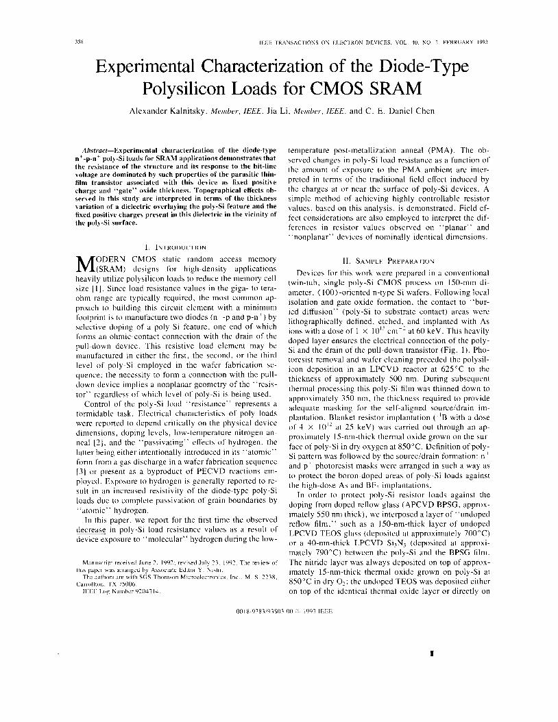
twin-tub. single poly-Si CMOS process on 150-mm di- ameter, ( 100)-oriented n-type Si wafers. Following local isolation and gate oxide formation, the contact to “bur- ied diffusion” (poly-Si to substrate contact) areas were lithographically defined, etched, and implanted with As ions with a dose of 1 x cm-’ at 60 keV. This heavily doped layer ensures the electrical connection of the poly- Si and the drain of the pull-down transistor (Fig. 1). Pho- toresist removal and wafer cleaning preceded the polysil- icon deposition in an LPCVD reactor at 625°C to the thickness of approximately 500 nm. During subsequent thermal processing this poly-Si film was thinned down to approximately 350 nm. the thickness required to provide adequate masking for the self-aligned sourceidrain im- plantation. Blanket resistor implantation (“B with a dose of 4 x IO’’ at 25 keV) was carried out through an ap- proximately IS-nm-thick thermal oxide grown on the sur- face ofpoly-Si in dry oxygen at 850°C. Definition of poly- Si pattern was followed by the sourceidrain formation: n + and pc photoresist masks were arranged in such a way as to protect the boron-doped areas of poly-Si loads against the high-dose As and BF, implantations.
In order to protect poly-Si resistor loads against the doping from doped reflow glass (APCVD BPSG, approx- imately 550 nm thick), we interposed a layer of “undoped reflow film,” such as a 150-nm-thick layer of undoped LPCVD TEOS glass (deposited at approximately 700°C) or a 40-nm-thick LPCVD Si,N3 (deposited at approxi- mately 790°C) between the poly-Si and the BPSG film. The nitride layer was always deposited on top of approx- imately 15-nm-thick thermal oxide grown on poly-Si at 850°C in dry 0:; the undoped TEOS was deposited either on top of the identical thermal oxide layer or directly on
0018 9183191501 00 I993 IEEE
KALNI I’SKY P I < I / C H A R A C T E R I Z A T I O N OF I‘Hk D I O D E - T Y P E POl.YSIl,ICOP! L0AI)S 359
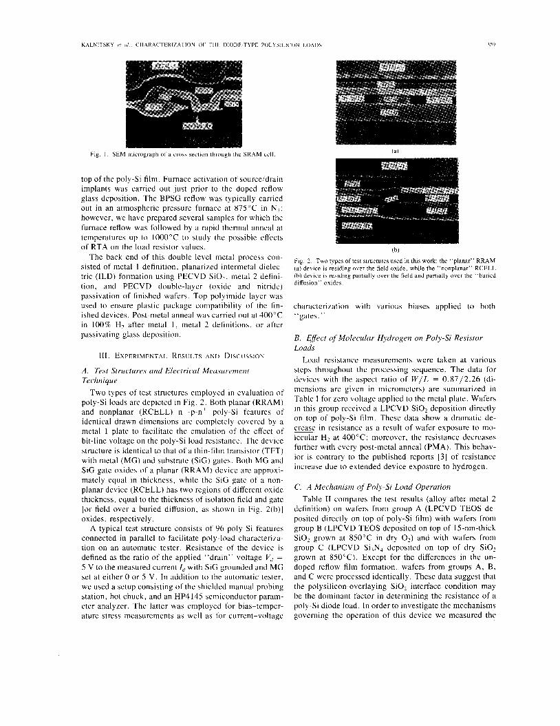
Fig. I . SEM micrograph of a cross section through the SRAM cell
top of the poly-Si film. Furnace activation of sourceidrain implants was carried out just prior to the doped reflow glass deposition. The BPSG reflow was typically carried out in an atmospheric pressure furnace at 875°C in N 2 ; however, we have prepared several samples for which the furnace reflow was followed by a rapid thermal anneal at temperatures up to 1000°C to study the possible effects of RTA on the load resistor values.
The back end of this double-level metal process con- sisted of metal 1 definition, planarized intermetal dielec- tric (ILD) formation using PECVD Si02 , metal 2 defini- tion, and PECVD double-layer (oxide and nitride) passivation of finished wafers. Top polyimide layer was used to ensure plastic package compatibility of the fin- ished devices. Post-metal anneal was carried out at 400°C in 100% H2 after metal 1, metal 2 definitions, or after passivating glass deposition.
111. EXPERIMENTAL RESULTS A N I ) DISCUSSION
A . Test Structures and Electrical Measiirement Technique
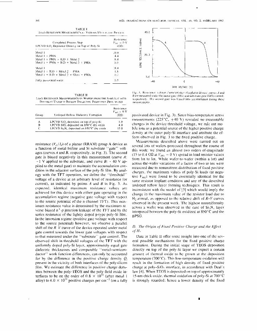
Two types of test structures employed in evaluation of poly-Si loads are depicted in Fig. 2. Both planar (RRAM) and nonplanar (RCELL) n+-p-n+ poly-Si features of identical drawn dimensions are completely covered by a metal 1 plate to facilitate the emulation of the effect of bit-line voltage on the poly-Si load resistance. The device structure is identical to that of a thin-film transistor (TFT) with metal (MG) and substrate (SiG) gates. Both MG and SiG gate oxides of a planar (RRAM) device are approxi- mately equal in thickness, while the SiG gate of a non- planar device (RCELL) has two regions of different oxide thickness, equal to the thickness of isolation field and gate [or field over a buried diffusion, as shown in Fig. 2(b)] oxides, respectively.
A typical test structure consists of 96 poly-Si features connected in parallel to facilitate poly-load characteriza- tion on an automatic tester. Resistance of the device is defined as the ratio of the applied “drain” voltage V,, = 5 V to the measured current IC, with SiG grounded and MG set at either 0 or 5 V. In addition to the automatic tester, we used a setup consisting of the shielded manual probing station, hot chuck, and an HP4 145 semiconductor param- eter analyzer. The latter was employed for bias-temper- ature stress measurements as well as for current-voltage
1 - 1
Fig. 2. Two types of test stmctures used in this work: the “planar” RRAM (a) device is residing over the field oxide, while the “nonplanar” RCELL (b) device is residing partially over the field and partially over the “buried diffusion” oxides.
characterization with various biases applied to both gates. ” “
B. Effect of Molecular Hydrogen on Poly-Si Resistor Loads
Load resistance measurements were taken at various steps throughout the processing sequence. The data for devices with the aspect ratio of W / L = 0.87/2.26 (di- mensions are given in micrometers) are summarized in Table I for zero voltage applied to the metal plate. Wafers in this group received a LPCVD SiOz deposition directly on top of poly-Si film. These data show a dramatic de- crease in resistance as a result of wafer exposure to mo- lecular H2 at 400°C; moreover, the resistance decreases further with every post-metal anneal (PMA). This behav- ior is contrary to the published reports [3] of resistance increase due to extended device exposure to hydrogen.
C. A Mechanism of Poly-Si Load Operation Table I1 compares the test results (alloy after metal 2
definition) on wafers from group A (LPCVD TEOS de- posited directly on top of poly-Si film) with wafers from group B (LPCVD TEOS deposited on top of 15-nm-thick Si02 grown at 850°C in dry 0,) and with wafers from group C (LPCVD SilN, deposited on top of dry SiOz grown at 850°C). Except for the differences in the un- doped reflow film formation, wafers from groups A, B, and C were processed identically. These data suggest that the polysilicon-overlaying SiO? interface condition may be the dominant factor in determining the resistance of a poly-Si diode load. In order to investigate the mechanisms governing the operation of this device we measured the
360 IEEE TRANSACTIONS ON ELECTRON DEVICES. VOL. 40. NO. 2 , FEBRUARY 1993
Resi\tance v,,,, = 0 v
(Gill Completed Procesh Step
LPCVD SiO, Deposited Directly on Top of Poly-Si
Metal I Metal I + PMA Metal I + PMA + ILD + Metal 2 Metal 1 + PMA + ILD + Metal 2 + PMA
Metal I Metal I + ILD + Metal 2 + PMA Metal 1 + ILD + Metal 2 + Glass + PMA
Fully pas\ivated wafer
10.0 4 . 3 6 4 0 . 5
18.0 I X 0.7
0 . 5
TABLE I1
DIFFFRENT UNDOPED REFLOW DIFLECTRIC FORMATION PROCFDLRES LOAD RESISTANCE MEASUREMENTS ON WAFERS FROM THE SAME LO1 WITH
Resistance v,, = 0 v
Group Undoped Reflow Dielectric Formation (Cia)
A LPCVD SiOz deposited on top of poly-Si I .o B LPCVD SiOz deposited on 850°C dry oxide 4.0 C LPCVD Si,N, deposited on 850°C dry oxide 15.0
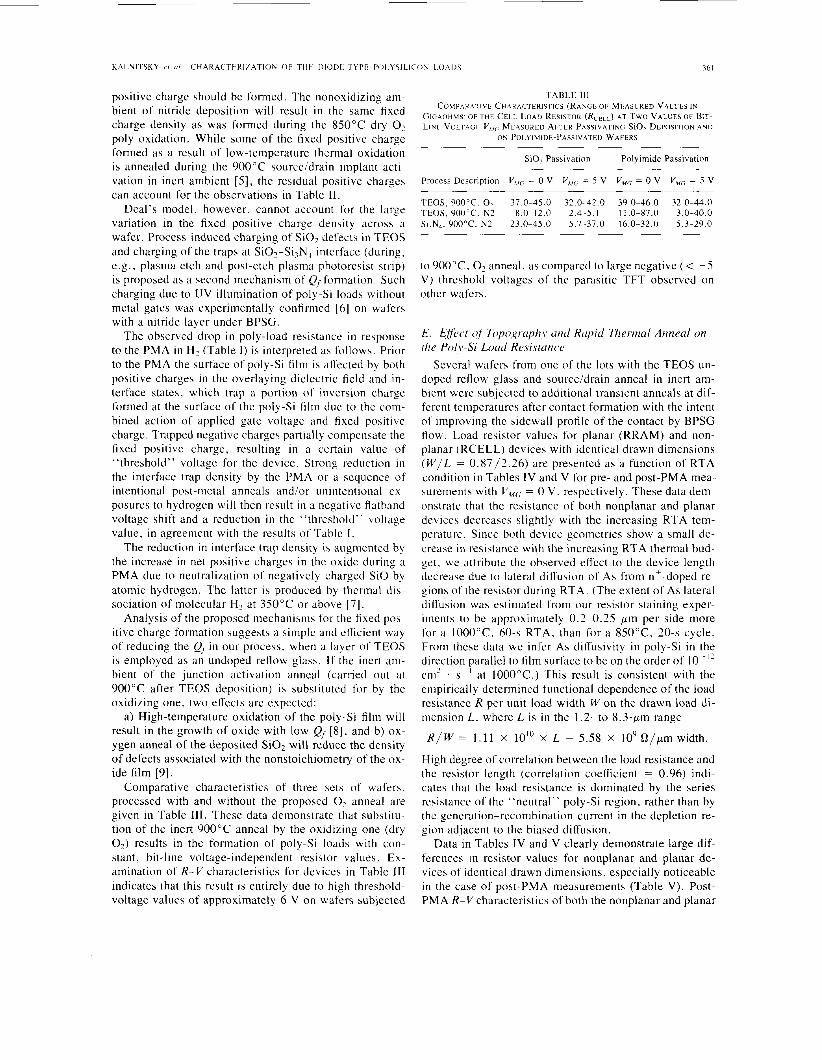
resistance ( Vd/Zd) of a planar (RRAM) group A device as a function of metal bitline and Si substrate “gate” volt- ages (curves A and B , respectively, in Fig. 3). The second gate is biased negatively in this measurement (curve A : - 1 V applied to the substrate, and curve B : -40 V ap- plied to the metal gate) to maintain the accumulation con- dition in the adjacent surface of the poly-Si film. By anal- ogy with the TFT operation, we define the “threshold” voltage of a device at an arbitrary level of resistance (or current), as indicated by points A and B in Fig. 3. As expected, identical maximum resistance values are achieved for this device with either gate operating in the accumulation regime (negative gate voltage with respect to the source potential of the n-channel TFT). This max- imum resistance value is determined by the maximum re- verse-biased nt-p junction leakage of the TFT and by the series resistance of the lightly doped p-type poly-Si film. In the inversion regime (positive gate voltage with respect to the source potential) however. we observe a parallel shift of the R- V curve of the device operated under metal gate control towards the lower gate voltages with respect to that measured under the “substrate” gate control. The observed shift in threshold voltages of the TFT with the uniformly doped poly-Si layer, approximately equal gate dielectric thicknesses and comparable “metal-semicon- ductor” work function differences, can only be accounted for by the difference in the positive charge density Q, present in the vicinity of both interfaces of the polysilicon film. We estimate the difference in positive charge dens- ities between the poly-TEOS and the poly-field oxide in- terfaces to be on the order of 0.8 X 10” (after metal 1 alloy) to 4.0 X 10” positive charges per cm-’ (on a fully
40.11
E r 8 w U z 4
Z 20.0 m w E
O Q 0 A
0.0
-40 0 +40
GATE VOLTAGE ( V )
Fig. 3 . Resistance-voltage characteristic of a planar device: curves A and B a r e nieawred under the metal gate (MG) and substrate gate (SiG) control. respectively. The second gate wa\ biased into accumulation during these nie;isurt‘nients.
passivated device in Fig. 3). Since bias-temperature stress measurements (22S°C, +40 V) revealed no measurable changes in the device threshold voltage, we rule out mo- bile ions as a potential source of the higher positive charge density at the outer poly-Si interface and attribute the ef- fects observed in Fig. 3 to the fixed positive charge.
Measurements described above were carried out on several lots of wafers processed throughout the course of this work: we found an almost two-orders-of-magnitude ( 15 to 0.4 GQ at VMG = 0 V) spread in load resistor values from lot to lot. While wafer-to-wafer (within a lot) and across-the-wafer variations of a factor of two to ten were measured due to nonuniform distribution of fixed positive charges. the maximum values of poly-Si loads (at nega- tive VM(;) were found to be essentially identical for the same resistor implant condition and any of the described undoped reflow layer forming techniques. This result is inconsistent with the model of 131 which would imply the change in the maximum value of the resistor load due to H1 anneal, as opposed to the relative shift of R-V curves observed in the present work. The highest nonuniformity across a wafer was observed in the case of Si3N4 layer interposed between the poly-Si oxidized at 850°C and the BPSG.
D. The Origin of Fixed Positiiv Churge and the Efect
Data in Table I1 offer some insight into one of the sev- eral possible mechanisms for the fixed positive charge formation. During the initial stage of TEOS deposition directly on top of the poly-Si layer we expect a certain amount of thermal oxide to be grown at the deposition temperature (700°C). This low-temperature oxidation will result in the formation of high density of fixed positive charge at poly-SiO, interface, in accordance with Deal’s law 141. When TEOS is deposited on top of approximately 15-nm-thick oxide, thermal oxidation of poly-Si at 700°C is strongly retarded; hence a lower density of the fixed
(f HI
1
positive charge should be formed. The nonoxidizing am- bient of nitride deposition will result in the same fixed charge density as was formed during the 850°C dry O2 poly oxidation. While some of the fixed positive charge formed as a result of low-temperature thermal oxidation is annealed during the 900°C sourceidrain implant acti- vation in inert ambient [ 5 ] , the residual positive charges can account for the observations in Table 11.
Deal's model, however. cannot account for the large variation in the fixed positive charge density across a wafer. Process-induced charging of S i02 defects in TEOS and charging of the traps at Si0,-Si3N, interface (during, e.g., plasma etch and post-etch plasma photoresist strip) is proposed as a second mechanism of Q, formation. Such charging due to UV illumination of poly-Si loads without metal gates was experimentally confirmed [6] on wafers with a nitride layer under BPSG.
The observed drop in poly-load resistance in response to the PMA in H2 (Table I ) is interpreted as follows. Prior to the PMA the surface of poly-Si film is affected by both positive charges in the overlaying dielectric field and in- terface states, which trap a portion of inversion charge formed at the surface of the poly-Si film due to the com- bined action of applied gate voltage and fixed positive charge. Trapped negative charges partially compensate the fixed positive charge, resulting in a certain value of "threshold" voltage for the device. Strong reduction in the interface trap density by the PMA or a sequence of intentional post-metal anneals and/or unintentional ex- posures to hydrogen will then result in a negative flatband voltage shift and a reduction in the "threshold" voltage value, in agreement with the results of Table I .
The reduction in interface trap density is augmented by the increase in net positive charges in the oxide during a PMA due to neutralization of negatively charged S i 0 by atomic hydrogen. The latter is produced by thermal dis- sociation of molecular H2 at 350°C or above [7].
Analysis of the proposed mechanisms for the fixed pos- itive charge formation suggests a simple and efficient way of reducing the Q, in our process, when a layer of TEOS is employed as an undoped reflow glass. If the inert am- bient of the junction activation anneal (carried out at 900°C after TEOS deposition) is substituted for by the oxidizing one, two effects are expected:
a) High-temperature oxidation of the poly-Si film will result in the growth of oxide with low Qf [8], and b) ox- ygen anneal of the deposited SiOz will reduce the density of defects associated with the nonstoichiometry of the ox- ide film [9].
Comparative characteristics of three sets of wafers, processed with and without the proposed O2 anneal are given in Table 111. These data demonstrate that substitu- tion of the inert 900°C anneal by the oxidizing one (dry 02) results in the formation of poly-Si loads with con- stant, bit-line voltage-independent resistor values. Ex- amination of R-V characteristics for devices in Table 111 indicates that this result is entirely due to high threshold- voltage values of approximately 6 V on wafers subjected
TABLE 111 COMPARA 1 I V E CHARACTERISTICS (RANGE OF MEASURED VALLIES I N
GIGAOHMS) OF r H E CELL LOAD RESISTOR (R,,,,) AT TWO VALCF,S OF BIT- LINT VOLTACF VMc; MEASURED AFTER PASSIVATING si02 DEPOSITION A N D
ON POLYIMIDE-PASSIVATED WAFERS
SiOL Passivation Polyimide Passivation
Process Description V,,,(, = 0 V Vu<; = 5 V V,,,G = 0 V VMc; = 5 V
TEOS, 900°C. O L 37.0-45.0 32.0-42.0 39.0-46.0 32.0-44.0 TEOS, 900°C. N2 8.0-12.0 2.4-5. I 11.0-87.0 3.0-40.0 Si7N,, 900°C. N2 23.0-45.0 5.7-37.0 16.0-32.0 5.3-29.0
to 900"C, O2 anneal, as compared to large negative (< -5 V ) threshold voltages of the parasitic TFT observed on other wafers.
E. E f rc t of Topngrupliy and Rupid Thermal Anneul on the Poly-Si Loud Resistcincr
Several wafers from one of the lots with the TEOS un- doped reflow glass and sourceidrain anneal in inert am- bient were subjected to additional transient anneals at dif- ferent temperatures after contact formation with the intent of improving the sidewall profile of the contact by BPSG flow. Load resistor values for planar (RRAM) and non- planar (RCELL) devices with identical drawn dimensions ( W / L = 0.87/2.26) are presented as a function of RTA condition in Tables IV and V for pre- and post-PMA mea- surements with VM(; = 0 V , respectively. These data dem- onstrate that the resistance of both nonplanar and planar devices decreases slightly with the increasing RTA tem- perature. Since both device geometries show a small de- crease in resistance with the increasing RTA thermal bud- get, we attribute the observed effect to the device length decrease due to lateral diffusion of As from n'-doped re- gions of the resistor during RTA. (The extent of As lateral diffusion was estimated from our resistor staining exper- iments to be approximately 0.2-0.25 pm per side more for a 10OO"C, 60-s RTA, than for a 850"C, 2 0 5 cycle. From these data we infer As diffusivity in poly-Si in the direction parallel to film surface to be on the order of IO-" c m 2 . s - I at 1000°C.) This result is consistent with the empirically determined functional dependence of the load resistance R per unit load width Won the drawn load di- mension L , where L is in the 1.2- to 8.3-pm range
R / W = 1.11 X 10" x L - 5.58 x lo9 Q/pm width.
High degree of correlation between the load resistance and the resistor length (correlation coefficient = 0.96) indi- cates that the load resistance is dominated by the series resistance of the "neutral" poly-Si region, rather than by the generation-recombination current in the depletion re- gion adjacent to the biased diffusion.
Data in Tables IV and V clearly demonstrate large dif- ferences in resistor values for nonplanar and planar de- vices of identical drawn dimensions, especially noticeable in the case of post-PMA measurements (Table V). Post- PMA R-V characteristics of both the nonplanar and planar
362
TABLE IV
FUNCTION ot RTA C O N D I T I O N S (Wafers with TEOS undoped reflow glass received an RTA after contact
ctch. All measurements were carried out prior to PMA.)
NONPIANAR ( R r , I I ) A N D PLANAR (RRA.,,) RESISIOR VAI U1:S 4\ A
~
IEEE TRANSACTIONS ON ELECTRON DEVICES, VOL. 40, NO. 2. FEBRUARY 1993
1000°C. 60 h 10.0 18.5 I000"C. 20 s I 1 .o 18.0 975°C. 60 s 12.0 19.5 975°C. 40 s 12.0 19.5 950°C. 60 s 12.0 20.0
TABLE V
FUNCTION OF RTA CONDITIOVS (Wafers with TEOS undoped reflow glass received on RTA after contact
etch. All measurements were carried out after PMA.)
NONPLANAR (RCEL, ) A N D PLANAR RESISTOR VALUES A S A
I000"C. 60 \ I000"C. 20 \ 975°C. 60 5
975"C, 40 b
950°C. 60 \
0.596 0.496 0.666 0.646 0 746
9.80 9.30
1 I .so
13.5 II 80
40.0 [ E L 0 0
w U
4
2 20.0 v) w G=
4 0 n
RTA C O N D I T I O N S
1. 9 5 0 C 60 s
2. 9 7 5 C 6 0 s
3. lO0OC 20 s
0 . 0 1 ' ' ' ?==-l2-. ' '
-40 0
GATE VOLTAGE ( V )
t40
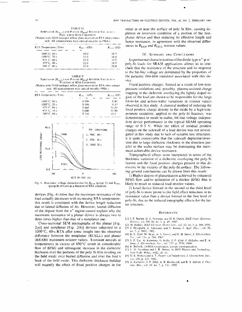
Fig. 4 . Resistance-voltage characteristics for R,,, (group A) and R,,,, (group B) devices as a function of RTA condition.
devices (Fig. 4) show that the maximum resistance of the load actually decreases with increasing RTA temperature: this result is consistent with the device length reduction due to lateral diffusion of As. However, lateral diffusion of the dopant from the n + region cannot explain why the maximum resistance of a planar device is always two to three times higher than that of a nonplanar one.
Cross-sectional SEM micrographs of the planar [Fig. 2(a)] and nonplanar [Fig. 2(b)] devices subjected to a 1000°C, 60-s RTA offer some insight into the observed difference between the nonplanar (RCELL) and planar (RRAM) maximum resistor values. Transient anneals at temperatures in excess of 850°C result in considerable flow of BPSG and subsequent increase in the dielectric thickness over the portions of the poly-Si film residing on the field oxide over buried diffusion and over the bird's beak of the field oxide. This dielectric thickness buildup will magnify the effect of fixed positive charges in the
oxide at or near the surface of poly-Si film, causing de- pletion or inversion condition of a portion of the non- planar device and thus reducing its effective length and hence resistance, in agreement with the observed differ- ences in RRAM and RCEL, resistor values.
IV. SUMMARY A N D CONCLUSIONS Experimental characterization of the diode-type n+-p-n
poly-Si loads for SRAM applications allows us to con- clude that the resistance of the structure and its response to the bit-line voltage are dominated by the properties of the parasitic thin-film transistor associated with this de- vice.
Fixed positive charges, formed as a result of low-tem- perature oxidations and, possibly, plasma-assisted charge trapping in the dielectric overlaying the lightly doped re- gion of the load are shown to be responsible for the large lot-to-lot and across-wafer variations in resistor values observed in this study. A classical method of reducing the fixed positive charge density in the oxide by a high-tem- perature oxidation, applied to the poly-Si features, was demonstrated to result in stable, bit-line voltage-indepen- dent device performance in the typical SRAM operating range of 0-5 V . While the effect of residual positive charges on the sidewall of a load device was not investi- gated in this study due to lack of suitable test structures, it is quite conceivable that the sidewall depletiodinver- sion due to large dielectric thickness in the direction par- allel to the wafer surface niay be dominating the maxi- mum achievable device resistance.
Topographical effects were interpreted in terms of the thickness variation of a dielectric overlaying the poly-Si feature and the fixed positive charges present in this di- electric in the vicinity of the poly-Si surface. The follow- ing general conclusions can be drawn from this result:
1 ) Higher degree of planarization achieved by enhanced BPSG flow and/or utilization of a thicker BPSG film is likely to result in reduced load resistor values.
2) Load device formed in the second or the third level of poly-Si is more prone to the field effect reduction in its resistance value than a device formed in the first level of poly-Si, due to the reduced topography effects for the lat- ter structure.
R t:F ER E N C ES
1 1 1 J . E . Mahan. D. S . Newman. and M. R. Gulett, lEEE Trans. Electron.
121 M. Rodder. IEEEElc,.c~/roii. D r i ? c ~ , L r r i . . v o l . 12. no. 4 , p. 160. 1991. 131 S . Hasegawa. S . Takenada. and Y Kurata. J . Appl . P h x s . . vol. 53,
no. 7. p. 5022. 1982. 141 B. E . Deal. M. Sklar. A. S . Gro\,c. and E . H. Snow, J . Elecrrochem.
S m . . vol. 114. p 266. 1967. 151 S . P. Tay. A . Kalnitsky. G. Kelly. J . P. Ellul, P. DeLalio, and E. A.
Irene. J . Electrochcrn. Soc.., vol. 137. p. 3579, 1990. 161 R. Bullock. INMOS Corporation. private communication. 171 E . H . Nicollian and J . R . Brews. i n MOS Physics rind Technology.
181 D. R. Wolten and A. T. Zcgers-van Duijnhoven, J . Electrochein. Soc..
191 A. Kalnitsky, J . P. Ellul. A. R . Boothroyd, and R. S . Abbott. J . E / P ( , -
Dcjrir,c~.\, vol . ED-30. n o . I . p. 45. 1983.
New York: Wiley. 1982, ch. I I
k o l . 139, p. 241. 1992.
f ro t i . MNI.. vol. 19. no. 2. p . 131. 1990.
Alexander Kalnitsky (M'88) received the M.S.E.E. degree from Odessa Institute of Technology, the M.A.Sc. degree from the University of To- ronto, Toronto, Ont.. Canada, and the Ph.D. degree from Carrleton Uni- versity. Ottawa, Ont. Canada.
From 1982 to 1990, he was employed by Northern Telecom Electronics Ltd., in Ottawa, where his research activities encompassed ellipsometry of multilayer structures. physics of oxide layers and its interfaces with Si, as well as submicrometer CMOS and BiCMOS. In 1990, he joined SGS- Thomson Microelectronics. Carrollton, TX. as a senior engineering section manager. responsible for technology transfers.
nt Profe\sor, before joining SGS-Thoiiison Microelcctronics in May 1990. His past research work included group theory and its application to solidhtate phyhics. energy band theor], ol sciiiiconductor\. transport theory of electrons in MOS invcrsion layers. radiation and hot-electron etfects o n MOS capacitors and MOSFET's, and MOS processing technology. Hc i \ currently working o n CMOS process integration and device physics.
Jia Li (M'92) rcceivcd h i \ College Diploma in
semiconductor devices and thc M.Sc. degree in
semiconductor physics in 1977 and 1981. respec- ti\cly. both from J i l in Universit) i n Changchun, China, and the Ph.D. degree in electrical engi- neering in 1988 from Yalc University. New Ha- ven. CT.
From October I988 to Ma) 1990. hc was uith thc Department of Electrical Enginccring a t the University of North Carolina. Charlotte. tirst as a post-doctoral Research Fellow and then as an As-
C. E. Daniel Chen received the B.S. degree in physics from National Tai- wan University, Taipei, Taiwan, in 1977 and the Ph.D. degree in physics from University of Pennsylvania, Philadelphia, in 1982.
He joined Texas Instruments Inc., Dallas, in May 1982, and worked on various silicon-on-insulator technologies including Stacked CMOS, Laser- Recrystallized SOI, FIPOS, and SIMOX. He became manager of the Sili- con Materials and Processing Branch in the Materials Science Laboratory in 1987. He joined SGS-Thomson Microelectronics, Carrollton, TX, in 1989, and is currently Device Engineering Manager.