Embed Size (px)
Citation preview
This content has been downloaded from IOPscience. Please scroll down to see the full text.
Download details:
IP Address: 137.138.139.20
This content was downloaded on 17/03/2014 at 15:29
Please note that terms and conditions apply.
Experimental characterization of the Clear-PEM scanner spectrometric performance
View the table of contents for this issue, or go to the journal homepage for more
2009 JINST 4 P10011
(http://iopscience.iop.org/1748-0221/4/10/P10011)
Home Search Collections Journals About Contact us My IOPscience
2009 JINST 4 P10011
PUBLISHED BY IOP PUBLISHING FOR SISSARECEIVED: July 8, 2009
ACCEPTED: September 28, 2009PUBLISHED: October 27, 2009
Experimental characterization of the Clear-PEMscanner spectrometric performance
R. Bugalho, a B. Carrico, a C.S. Ferreira, a M. Frade,a,1 M. Ferreira, a R. Moura, a
C. Ortig ao,a J.F. Pinheiro, a P. Rodrigues, a I. Rolo, a J.C. Silva, a A. Trindade a andJ. Varela a,b,c
aLaboratorio de Instrumentacao e Fısica Experimental de Partıculas (LIP),Av. Elias Garcia 14-1, 1000-149 Lisboa, Portugal
bInstituto Superior Tecnico (IST) da Universidade Tecnica de Lisboa,Av. Rovisco Pais, 1049-001 Lisboa, Portugal
cEuropean Organization for Nuclear Research (CERN),CH-1211 Geneve 23, Switzerland
E-mail: [email protected]
ABSTRACT: In the framework of the Clear-PEM project for the construction of a high-resolutionand high-specificity scanner for breast cancer imaging, a Positron Emission Mammography tomo-graph has been developed and installed at theInstituto Portugues de Oncologia do Portohospital.The Clear-PEM scanner is mainly composed by two planar detector heads attached to a roboticarm, trigger/data acquisition electronics system and computing servers. The detector heads holdcrystal matrices built from 2×2×20 mm3 LYSO:Ce crystals readout by Hamamatsu S8550 APDarrays. The APDs are optically coupled to both ends of the 6144 crystals in order to extract theDOI information for each detected event. Each one of 12288 APD’s pixels is read and controlled byApplication Specific Integrated Circuits water-cooled by an external cooling unit. The Clear-PEMfrontend boards innovative design results in a unprecedented integration of the crystal matrices,APDs and ASICs, making Clear-PEM the PET scanner with the highest number of APD pixelsever integrated so far.
In this paper, the scanner’s main technical characteristics, calibration strategies and the firstspectrometric performance evaluation in a clinical environment are presented.
The first commissioning results show 99.7% active channels,which, after calibration, haveinter-pixel and absolute gain distributions with dispersions of, respectively, 12.2% and 15.3%,demonstrating that despite the large number of channels, the system is uniform. The mean en-ergy resolution at 511 keV is of 15.9%, with a 8.8% dispersion, and the meanC−1
DOI is 5.9%/mm,with a 7.8% dispersion. The coincidence time resolution, at511 keV, for a energy window between400 and 600 keV, is 5.2 ns FWHM.
KEYWORDS: Gamma camera, SPECT, PET PET/CT, coronary CT angiography (CTA); Photon de-tectors for UV, visible and IR photons (solid-state) (PIN diodes, APDs, Si-PMTs, CCDs, EBCCDsetc); Front-end electronics for detector readout
1Corresponding author.
c© 2009 IOP Publishing Ltd and SISSA doi:10.1088/1748-0221/4/10/P10011
2009 JINST 4 P10011
Contents
1 Introduction 1
2 The Clear-PEM scanner 2
3 Calibration methods 33.1 Energy calibration 43.2 DOI calibration 43.3 Time calibration 5
4 Experimental results from the Clear-PEM integration phase 74.1 Noise measurements 74.2 Pulse shape 94.3 Time resolution 104.4 Energy measurements 12
5 Conclusions 16
1 Introduction
One in every eleven Portuguese women are diagnosed with Breast Cancer, which makes it one ofthe most common cancers and the leading cause of death by cancer for women between the agesof 35 and 55 [1]. This incidence rate value is similar to most developed countries. If diagnosedcorrectly and on its early stages, the 5-year relative survival rate is higher than 90%. However,the most common and wide-spread diagnostic technique, X-ray mammography, can only provideanatomical information of the breast tissues, resulting ina high false-positive rate, specially indense breasts. There is therefore a great need for a breast cancer diagnosis system with both a highspecificity and a high resolution. Positron Emission Tomography (PET) imaging [2], in which theClear-PEM scanner is based, presents itself as a viable solution to this need.
PET whole-body scanners using18F-FDG as a radioactive tracer and dual-time-point imaging,have a sensitivity higher than 90% for breast tumors larger than 1 cm, but lesions with less than 1 cmin diameter can be undetected [3]. To solve this problem it is necessary to design PET scannersexclusively for breast imaging, known as Positron EmissionMammography scanners (PEM) [4, 5].The Clear-PEM scanner was thus designed to have high sensitivity, high specificity and a goodspatial resolution in order to detect small tumors, both on the breast and axilla regions [6, 7].
Unlike in common ring-shaped PET scanners, the Clear-PEM’sdetector plates are very closeto each other, increasing the parallax effect [8]. This effect occurs when the interaction point ofthe photon that penetrates into the detector module is assigned to the front face of the detectorelement, introducing a mispositioning in the Line-of-Response (LOR). If the depth-of-interaction
– 1 –
2009 JINST 4 P10011
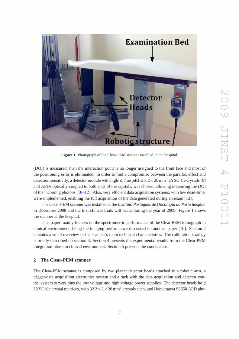
Figure 1. Photograph of the Clear-PEM scanner installed in the hospital.
(DOI) is measured, then the interaction point is no longer assigned to the front face and most ofthe positioning error is eliminated. In order to find a compromise between the parallax effect anddetection sensitivity, a detector module with high-Z, fine pitch 2×2×20 mm3 LYSO:Ce crystals [9]and APDs optically coupled to both ends of the crystals, was chosen, allowing measuring the DOIof the incoming photons [10–12]. Also, very efficient data acquisition systems, with low dead-time,were implemented, enabling the full acquisition of the datagenerated during an exam [13].
The Clear-PEM scanner was installed at theInstituto Portugues de Oncologia do Portohospitalin December 2008 and the first clinical trials will occur during the year of 2009. Figure1 showsthe scanner at the hospital.
This paper mainly focuses on the spectrometric performanceof the Clear-PEM tomograph inclinical environment, being the imaging performance discussed on another paper [10]. Section 2contains a small overview of the scanner’s main technical characteristics. The calibration strategyis briefly described on section 3. Section 4 presents the experimental results from the Clear-PEMintegration phase in clinical environment. Section 5 presents the conclusions.
2 The Clear-PEM scanner
The Clear-PEM scanner is composed by two planar detector heads attached to a robotic arm, atrigger/data acquisition electronics system and a rack with the data acquisition and detector con-trol system servers plus the low voltage and high voltage power supplies. The detector heads holdLYSO:Ce crystal matrices, with 32 2×2×20 mm3 crystals each, and Hamamatsu S8550 APD pho-
– 2 –
2009 JINST 4 P10011
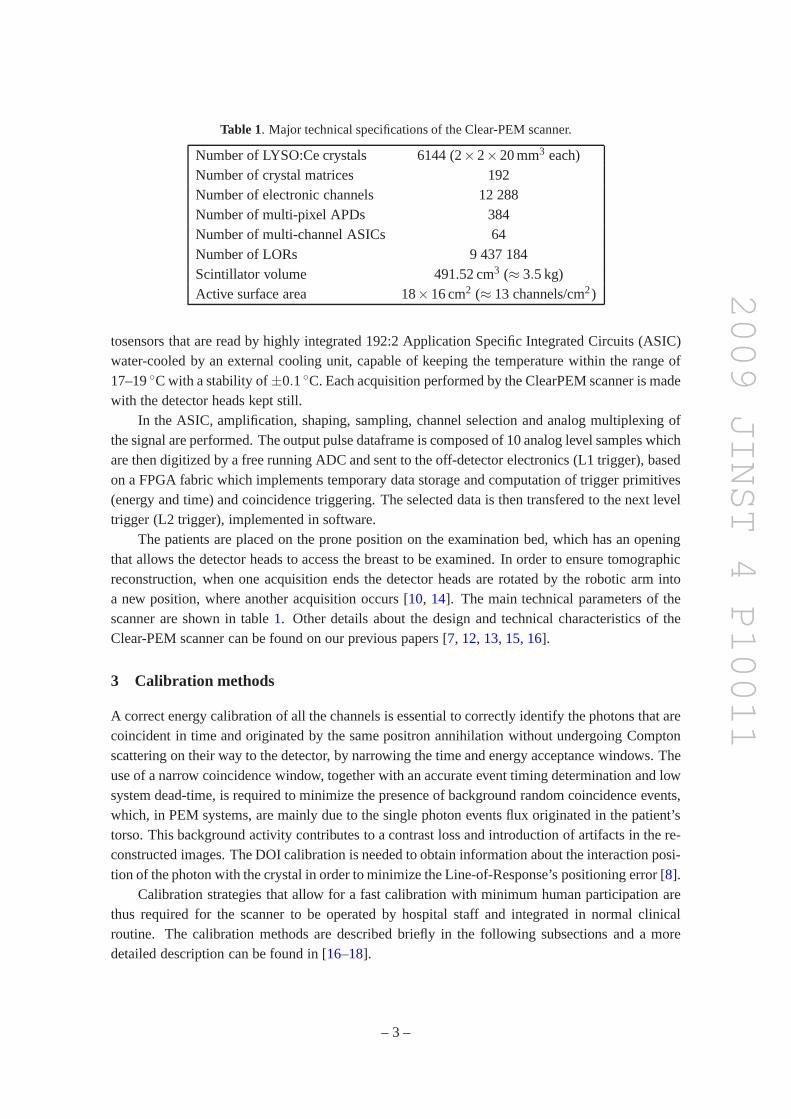
Table 1. Major technical specifications of the Clear-PEM scanner.
Number of LYSO:Ce crystals 6144 (2×2×20 mm3 each)Number of crystal matrices 192Number of electronic channels 12 288Number of multi-pixel APDs 384Number of multi-channel ASICs 64Number of LORs 9 437 184Scintillator volume 491.52 cm3 (≈ 3.5 kg)Active surface area 18×16 cm2 (≈ 13 channels/cm2)
tosensors that are read by highly integrated 192:2 Application Specific Integrated Circuits (ASIC)water-cooled by an external cooling unit, capable of keeping the temperature within the range of17–19◦C with a stability of±0.1◦C. Each acquisition performed by the ClearPEM scanner is madewith the detector heads kept still.
In the ASIC, amplification, shaping, sampling, channel selection and analog multiplexing ofthe signal are performed. The output pulse dataframe is composed of 10 analog level samples whichare then digitized by a free running ADC and sent to the off-detector electronics (L1 trigger), basedon a FPGA fabric which implements temporary data storage andcomputation of trigger primitives(energy and time) and coincidence triggering. The selecteddata is then transfered to the next leveltrigger (L2 trigger), implemented in software.
The patients are placed on the prone position on the examination bed, which has an openingthat allows the detector heads to access the breast to be examined. In order to ensure tomographicreconstruction, when one acquisition ends the detector heads are rotated by the robotic arm intoa new position, where another acquisition occurs [10, 14]. The main technical parameters of thescanner are shown in table1. Other details about the design and technical characteristics of theClear-PEM scanner can be found on our previous papers [7, 12, 13, 15, 16].
3 Calibration methods
A correct energy calibration of all the channels is essential to correctly identify the photons that arecoincident in time and originated by the same positron annihilation without undergoing Comptonscattering on their way to the detector, by narrowing the time and energy acceptance windows. Theuse of a narrow coincidence window, together with an accurate event timing determination and lowsystem dead-time, is required to minimize the presence of background random coincidence events,which, in PEM systems, are mainly due to the single photon events flux originated in the patient’storso. This background activity contributes to a contrast loss and introduction of artifacts in the re-constructed images. The DOI calibration is needed to obtaininformation about the interaction posi-tion of the photon with the crystal in order to minimize the Line-of-Response’s positioning error [8].
Calibration strategies that allow for a fast calibration with minimum human participation arethus required for the scanner to be operated by hospital staff and integrated in normal clinicalroutine. The calibration methods are described briefly in the following subsections and a moredetailed description can be found in [16–18].
– 3 –
2009 JINST 4 P10011
3.1 Energy calibration
The energy of every detected hit is given by the sum of the energies measured by the two APDs thatreadout the top and bottom ends of the crystal where the photon interacted. It is then required thatboth APDs have an equalized gain. Taking advantage of the natural presence of176Lu within theLYSO:Ce crystal, uniformly distributed along its entire volume, the inter-pixel gain is determinedby assuming that the energy spectra of each APD should be the same. Taking as reference the topAPD’s spectrum, aKrel constant is multiplied by the amplitude of the bottom APD signal. Oncethe gain of the APDs is equalized, the top-bottom summed spectrum can be calibrated in energy byfinding the position of the 511 keV peak emitted by either a68Ge or a22Na source and computingthe absolute gain constantKabs. The energy of each event, in keV, is then estimated by:
E = Kabs(Et +KrelEb) (3.1)
whereEt andEb are the values of the pedestal-subtracted pulse’s amplitude of the top and bottomAPDs, respectively.
To find the correctKrel, the bottom and top APD spectrum for a single crystal are comparedand aχ2 distribution, that measures the similarity between the spectrum, is computed. Thisdistribution’s minimum value is then determined, corresponding toKrel. The distribution is de-fined as [7, 19]:
χ2 =N
∑i=1
(
ψ it −Krelψ i
b
)2
ψ it +Krelψ i
b
(3.2)
whereψ it andψ i
b are the number of entries in eachi bin of the energy spectra of the top and bottomAPD, respectively, and N is the total number of bins.
3.2 DOI calibration
The interaction depth of a photon,z, is computed from the asymmetry of light collection betweenthe two APDs that readout the light of a given crystal by:
z= CDOIEt −KrelEb
Et +KrelEb(3.3)
TheCDOI constant transforms the ratio of shared light into a physical distance unit and is obtainedright afterKrel calibration, also using the176Lu present in the crystal. This constant is then deter-mined by finding the edges of the asymmetry distribution, which is uniform due to the uniform con-centration of the176Lu decays along the crystal [20]. From this assumption,CDOI is estimated by:
CDOI =20 mm
(Asymmetry at positive edge)− (Asymmetry at negative edge)(3.4)
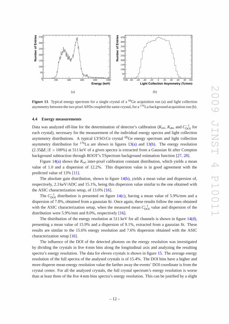
whereAsymmetry at positive edgeandAsymmetry at negative edgeare the asymmetry values onthe corresponding crystal edges, extracted from a light collection asymmetry plot like the oneshown in figure13(b)[20].
– 4 –
2009 JINST 4 P10011
Time (ns)0 50 100 150 200 250 300 350 400
Am
plitu
de (
Arb
. Uni
ts)
0
0.2
0.4
0.6
0.8
1
peakT
maxT
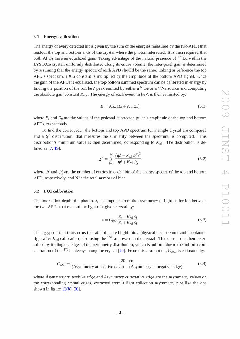
Figure 2. Pulse shape parameterizationf (t).
3.3 Time calibration
To discriminate between two photon events of the same decay from uncorrelated single photonsfrom distinct decays, a PET system needs to be able to extractthe time information from eachinteraction with a resolution of about a few nanoseconds [21, 22].
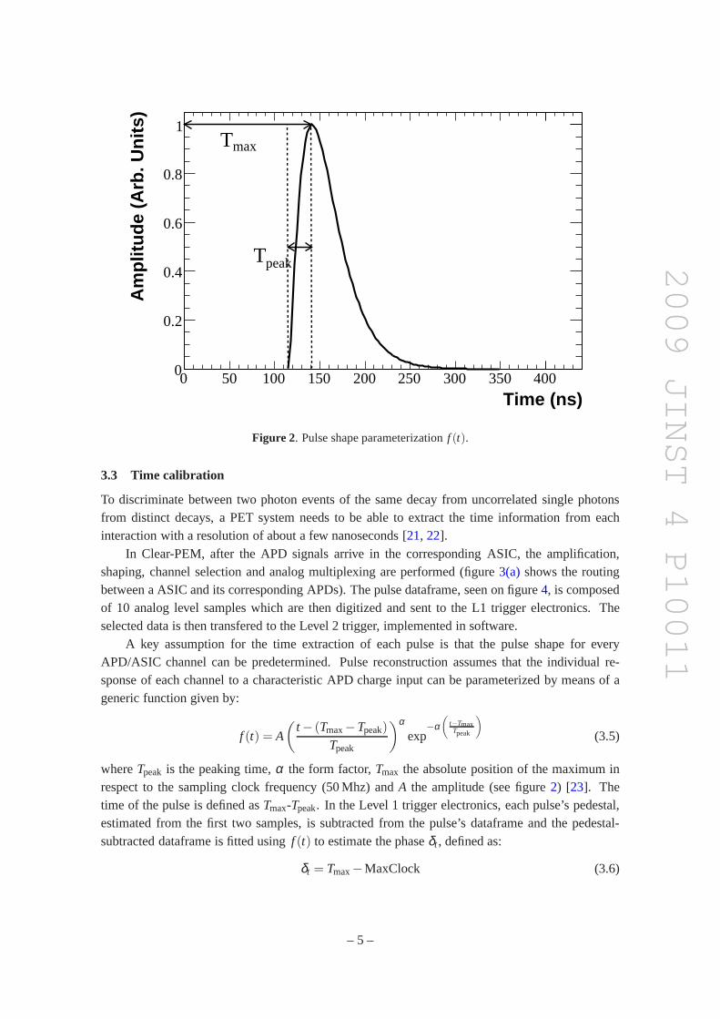
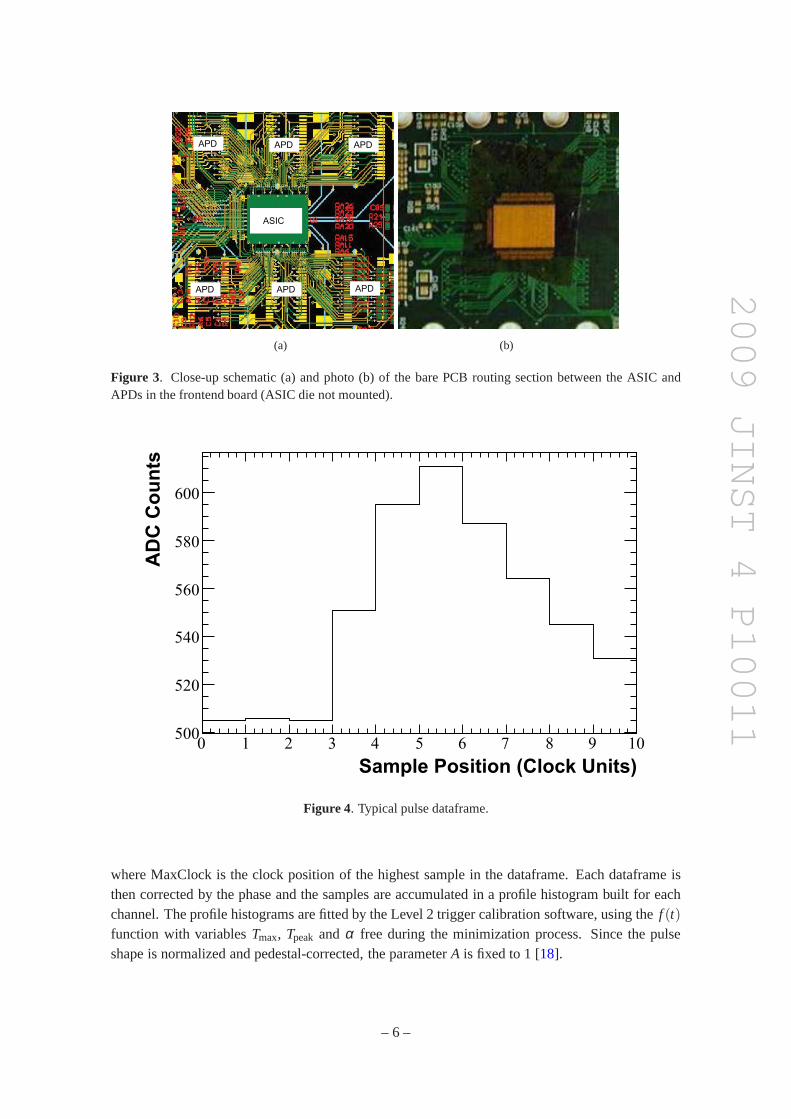
In Clear-PEM, after the APD signals arrive in the corresponding ASIC, the amplification,shaping, channel selection and analog multiplexing are performed (figure3(a) shows the routingbetween a ASIC and its corresponding APDs). The pulse dataframe, seen on figure4, is composedof 10 analog level samples which are then digitized and sent to the L1 trigger electronics. Theselected data is then transfered to the Level 2 trigger, implemented in software.
A key assumption for the time extraction of each pulse is thatthe pulse shape for everyAPD/ASIC channel can be predetermined. Pulse reconstruction assumes that the individual re-sponse of each channel to a characteristic APD charge input can be parameterized by means of ageneric function given by:
f (t) = A
(
t − (Tmax−Tpeak)
Tpeak
)αexp
−α(
t−TmaxTpeak
)
(3.5)
whereTpeak is the peaking time,α the form factor,Tmax the absolute position of the maximum inrespect to the sampling clock frequency (50 Mhz) andA the amplitude (see figure2) [23]. Thetime of the pulse is defined asTmax-Tpeak. In the Level 1 trigger electronics, each pulse’s pedestal,estimated from the first two samples, is subtracted from the pulse’s dataframe and the pedestal-subtracted dataframe is fitted usingf (t) to estimate the phaseδt , defined as:
δt = Tmax−MaxClock (3.6)
– 5 –
2009 JINST 4 P10011
ASIC
APD
APD
APD APD
APD APD
(a) (b)
Figure 3. Close-up schematic (a) and photo (b) of the bare PCB routingsection between the ASIC andAPDs in the frontend board (ASIC die not mounted).
Sample Position (Clock Units)
0 1 2 3 4 5 6 7 8 9 10
AD
C C
ou
nts
500
520
540
560
580
600
Figure 4. Typical pulse dataframe.
where MaxClock is the clock position of the highest sample inthe dataframe. Each dataframe isthen corrected by the phase and the samples are accumulated in a profile histogram built for eachchannel. The profile histograms are fitted by the Level 2 trigger calibration software, using thef (t)function with variablesTmax, Tpeak andα free during the minimization process. Since the pulseshape is normalized and pedestal-corrected, the parameterA is fixed to 1 [18].
– 6 –
2009 JINST 4 P10011
Elapsed Time (seconds)
1000 2000 3000 4000 5000 6000
Te
mp
era
ture
(C
els
ius
)
17.5
17.6
17.7
17.8
17.9
18
18.1
18.2
18.3
18.4
18.5
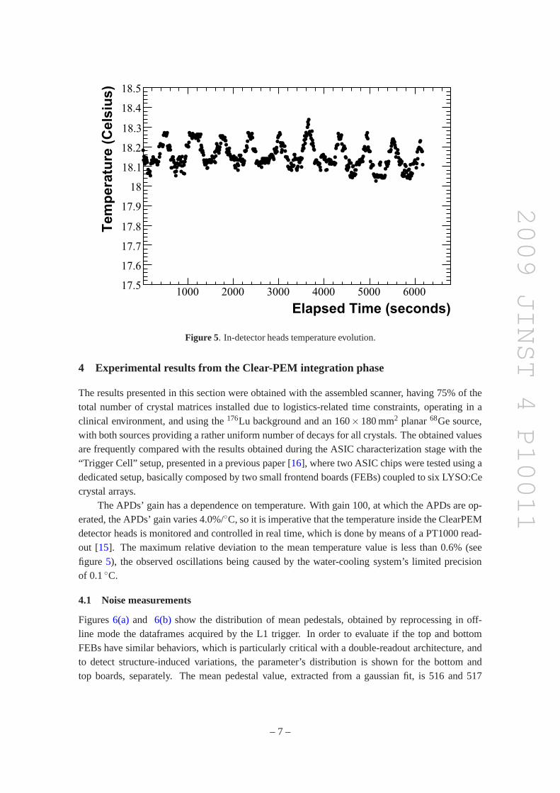
Figure 5. In-detector heads temperature evolution.
4 Experimental results from the Clear-PEM integration phase
The results presented in this section were obtained with theassembled scanner, having 75% of thetotal number of crystal matrices installed due to logistics-related time constraints, operating in aclinical environment, and using the176Lu background and an 160×180 mm2 planar68Ge source,with both sources providing a rather uniform number of decays for all crystals. The obtained valuesare frequently compared with the results obtained during the ASIC characterization stage with the“Trigger Cell” setup, presented in a previous paper [16], where two ASIC chips were tested using adedicated setup, basically composed by two small frontend boards (FEBs) coupled to six LYSO:Cecrystal arrays.
The APDs’ gain has a dependence on temperature. With gain 100, at which the APDs are op-erated, the APDs’ gain varies 4.0%/◦C, so it is imperative that the temperature inside the ClearPEMdetector heads is monitored and controlled in real time, which is done by means of a PT1000 read-out [15]. The maximum relative deviation to the mean temperature value is less than 0.6% (seefigure 5), the observed oscillations being caused by the water-cooling system’s limited precisionof 0.1◦C.
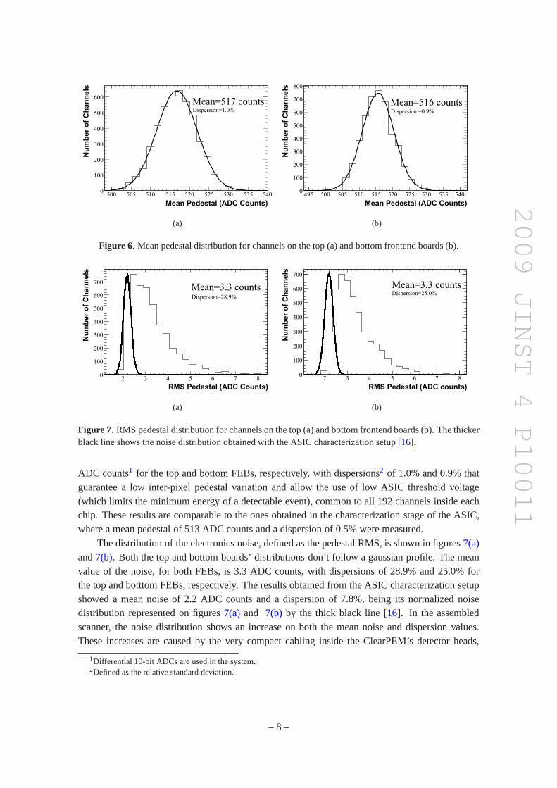
4.1 Noise measurements
Figures6(a) and 6(b) show the distribution of mean pedestals, obtained by reprocessing in off-line mode the dataframes acquired by the L1 trigger. In orderto evaluate if the top and bottomFEBs have similar behaviors, which is particularly critical with a double-readout architecture, andto detect structure-induced variations, the parameter’s distribution is shown for the bottom andtop boards, separately. The mean pedestal value, extractedfrom a gaussian fit, is 516 and 517
– 7 –
2009 JINST 4 P10011
Mean Pedestal (ADC Counts)
500 505 510 515 520 525 530 535 540
Nu
mb
er
of
Ch
an
ne
ls
0
100
200
300
400
500
600Mean=517 countsDispersion=1.0%
(a)
Mean Pedestal (ADC Counts)
495 500 505 510 515 520 525 530 535 540
Nu
mb
er
of
Ch
an
ne
ls
0
100
200
300
400
500
600
700
800
Mean=516 countsDispersion =0.9%
(b)
Figure 6. Mean pedestal distribution for channels on the top (a) and bottom frontend boards (b).
RMS Pedestal (ADC Counts)
2 3 4 5 6 7 8
Nu
mb
er
of
Ch
an
ne
ls
0
100
200
300
400
500
600
700Mean=3.3 countsDispersion=28.9%
(a)
RMS Pedestal (ADC counts)
2 3 4 5 6 7 8
Nu
mb
er
of
Ch
an
ne
ls
0
100
200
300
400
500
600
700
Mean=3.3 countsDispersion=25.0%
(b)
Figure 7. RMS pedestal distribution for channels on the top (a) and bottom frontend boards (b). The thickerblack line shows the noise distribution obtained with the ASIC characterization setup [16].
ADC counts1 for the top and bottom FEBs, respectively, with dispersions2 of 1.0% and 0.9% thatguarantee a low inter-pixel pedestal variation and allow the use of low ASIC threshold voltage(which limits the minimum energy of a detectable event), common to all 192 channels inside eachchip. These results are comparable to the ones obtained in the characterization stage of the ASIC,where a mean pedestal of 513 ADC counts and a dispersion of 0.5% were measured.
The distribution of the electronics noise, defined as the pedestal RMS, is shown in figures7(a)and7(b). Both the top and bottom boards’ distributions don’t followa gaussian profile. The meanvalue of the noise, for both FEBs, is 3.3 ADC counts, with dispersions of 28.9% and 25.0% forthe top and botttom FEBs, respectively. The results obtained from the ASIC characterization setupshowed a mean noise of 2.2 ADC counts and a dispersion of 7.8%,being its normalized noisedistribution represented on figures7(a) and 7(b) by the thick black line [16]. In the assembledscanner, the noise distribution shows an increase on both the mean noise and dispersion values.These increases are caused by the very compact cabling inside the ClearPEM’s detector heads,
1Differential 10-bit ADCs are used in the system.2Defined as the relative standard deviation.
– 8 –
2009 JINST 4 P10011
Time (ns)
0 20 40 60 80 100 120 140 160
No
rma
lize
d P
uls
e
0
0.2
0.4
0.6
0.8
1
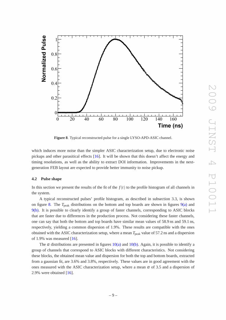
Figure 8. Typical reconstructed pulse for a single LYSO-APD-ASIC channel.
which induces more noise than the simpler ASIC characterization setup, due to electronic noisepickups and other parasitical effects [16]. It will be shown that this doesn’t affect the energy andtiming resolutions, as well as the ability to extract DOI information. Improvements in the next-generation FEB layout are expected to provide better immunity to noise pickup.
4.2 Pulse shape
In this section we present the results of the fit of thef (t) to the profile histogram of all channels inthe system.
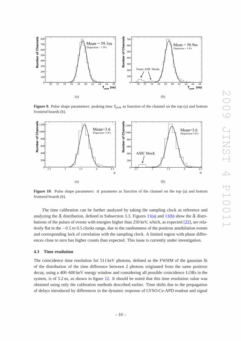
A typical reconstructed pulses’ profile histogram, as described in subsection 3.3, is shownon figure8. The Tpeak distributions on the bottom and top boards are shown in figures 9(a) and9(b). It is possible to clearly identify a group of faster channels, corresponding to ASIC blocksthat are faster due to differences in the production process. Not considering these faster channels,one can say that both the bottom and top boards have similar mean values of 58.9 ns and 59.1 ns,respectively, yielding a common dispersion of 1.9%. These results are compatible with the onesobtained with the ASIC characterization setup, where a meanTpeakvalue of 57.2 ns and a dispersionof 1.9% was measured [16].
Theα distributions are presented in figures10(a)and10(b). Again, it is possible to identify agroup of channels that correspond to ASIC blocks with different characteristics. Not consideringthese blocks, the obtained mean value and dispersion for both the top and bottom boards, extractedfrom a gaussian fit, are 3.6% and 3.8%, respectively. These values are in good agreement with theones measured with the ASIC characterization setup, where ameanα of 3.5 and a dispersion of2.9% were obtained [16].
– 9 –
2009 JINST 4 P10011
(ns)peak
T50 52 54 56 58 60 62 64 66 68
Nu
mb
er
of
Ch
an
ne
ls
0
100
200
300
400
500
600
700
800
Mean = 59.1nsDispersion = 1.9%
(a)
(ns)peak
T50 52 54 56 58 60 62 64 66 68
Nu
mb
er
of
Ch
an
ne
ls
0
100
200
300
400
500
600
700
Mean = 58.9nsDispersion = 1.9%
Faster ASIC blocks
(b)
Figure 9. Pulse shape parameters: peaking timeTpeak as function of the channel on the top (a) and bottomfrontend boards (b).
α
2.5 3 3.5 4 4.5
Nu
mb
er
of
Ch
an
ne
ls
0
200
400
600
800
1000
1200
Mean=3.6Dispersion=3.8%
(a)
α
2.5 3 3.5 4 4.5
Nu
mb
er
of
Ch
an
ne
ls
0
200
400
600
800
1000
1200
ASIC block
Mean=3.6Dispersion=3.8%
(b)
Figure 10. Pulse shape parameters:α parameter as function of the channel on the top (a) and bottomfrontend boards (b).
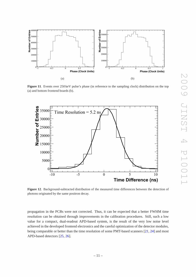
The time calibration can be further analyzed by taking the sampling clock as reference andanalyzing theδt distribution, defined in Subsection 3.3. Figures11(a)and11(b)show theδt distri-butions of the pulses of events with energies higher than 250keV, which, as expected [22], are rela-tively flat in the−0.5 to 0.5 clocks range, due to the randomness of the positron annihilation eventsand corresponding lack of correlation with the sampling clock. A limited region with phase differ-ences close to zero has higher counts than expected. This issue is currently under investigation.
4.3 Time resolution
The coincidence time resolution for 511 keV photons, definedas the FWHM of the gaussian fitof the distribution of the time difference between 2 photonsoriginated from the same positrondecay, using a 400–600 keV energy window and considering allpossible coincidence LORs in thesystem, is of 5.2 ns, as shown in figure12. It should be noted that this time resolution value wasobtained using only the calibration methods described earlier. Time shifts due to the propagationof delays introduced by differences in the dynamic responseof LYSO:Ce-APD readout and signal
– 10 –
2009 JINST 4 P10011
Phase (Clock Units)
-1 -0.5 0 0.5 1
Nu
mb
er
of
En
trie
s
0
10000
20000
30000
40000
50000
60000
(a)
Phase (Clock Units)
-1 -0.5 0 0.5 1
Nu
mb
er
of
En
trie
s
0
10000
20000
30000
40000
50000
(b)
Figure 11. Events over 250 keV pulse’s phase (in reference to the sampling clock) distribution on the top(a) and bottom frontend boards (b).
Time Difference (ns)
-10 -5 0 5 10
Nu
mb
er
of
En
trie
s
0
5000
10000
15000
20000
25000
30000
35000 Time Resolution = 5.2 ns
Figure 12. Background-subtracted distribution of the measured timedifferences between the detection ofphotons originated by the same positron decay.
propagation in the PCBs were not corrected. Thus, it can be expected that a better FWHM timeresolution can be obtained through improvements in the calibration procedures. Still, such a lowvalue for a compact, dual-readout APD-based system, is the result of the very low noise levelachieved in the developed frontend electronics and the careful optimization of the detector modules,being comparable or better than the time resolution of some PMT-based scanners [21, 24] and mostAPD-based detectors [25, 26].
– 11 –
2009 JINST 4 P10011
Energy (keV)
0 200 400 600 800 1000
Nu
mb
er
of
En
trie
s
0
50
100
150
200
250
300
350
(a)
Light Collection Asymmetry (%/mm)
-100 -80 -60 -40 -20 0 20 40 60 80 100
Nu
mb
er
of
En
trie
s
0
50
100
150
200
250
300
350
400
450
(b)
Figure 13. Typical energy spectrum for a single crystal of a68Ge acquisition run (a) and light collectionasymmetry between the two pixel APDs coupled the same crystal, for a176Lu background acquisition run (b).
4.4 Energy measurements
Data was analyzed off-line for the determination of detector’s calibration (Krel, Kabs andC−1DOI for
each crystal), necessary for the measurement of the individual energy spectra and light collectionasymmetry distributions. A typical LYSO:Ce crystal68Ge energy spectrum and light collectionasymmetry distribution for176Lu are shown in figures13(a) and 13(b). The energy resolution(2.35∆E/E×100%) at 511 keV of a given spectra is extracted from a Gaussian fit after Comptonbackground subtraction through ROOT’s TSpectrum background estimation function [27, 28].
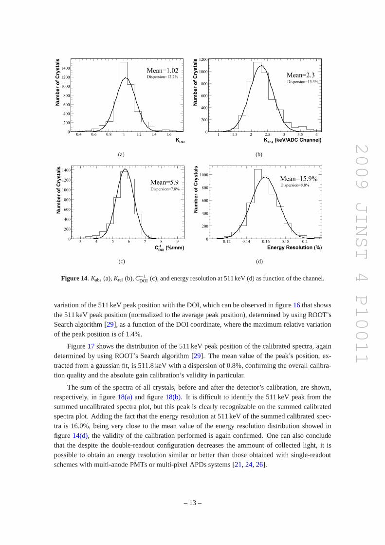
Figure14(a)shows theKrel inter-pixel calibration constant distribution, which yields a meanvalue of 1.0 and a dispersion of 12.2%. This dispersion valueis in good agreement with thepredicted value of 13% [11].
The absolute gain distribution, shown in figure14(b), yields a mean value and dispersion of,respectively, 2.3 keV/ADC and 15.1%, being this dispersionvalue similar to the one obtained withthe ASIC characterization setup, of 13.0% [16].
TheC−1DOI distribution is presented on figure14(c), having a mean value of 5.9%/mm and a
dispersion of 7.8%, obtained from a gaussian fit. Once again,these results follow the ones obtainedwith the ASIC characterization setup, when the measured mean C−1
DOI value and dispersion of thedistribution were 5.9%/mm and 8.0%, respectively [16].
The distribution of the energy resolution at 511 keV for all channels is shown in figure14(d),presenting a mean value of 15.9% and a dispersion of 9.1%, extracted from a gaussian fit. Theseresults are similar to the 15.6% energy resolution and 7.6% dispersion obtained with the ASICcharacterization setup [16].
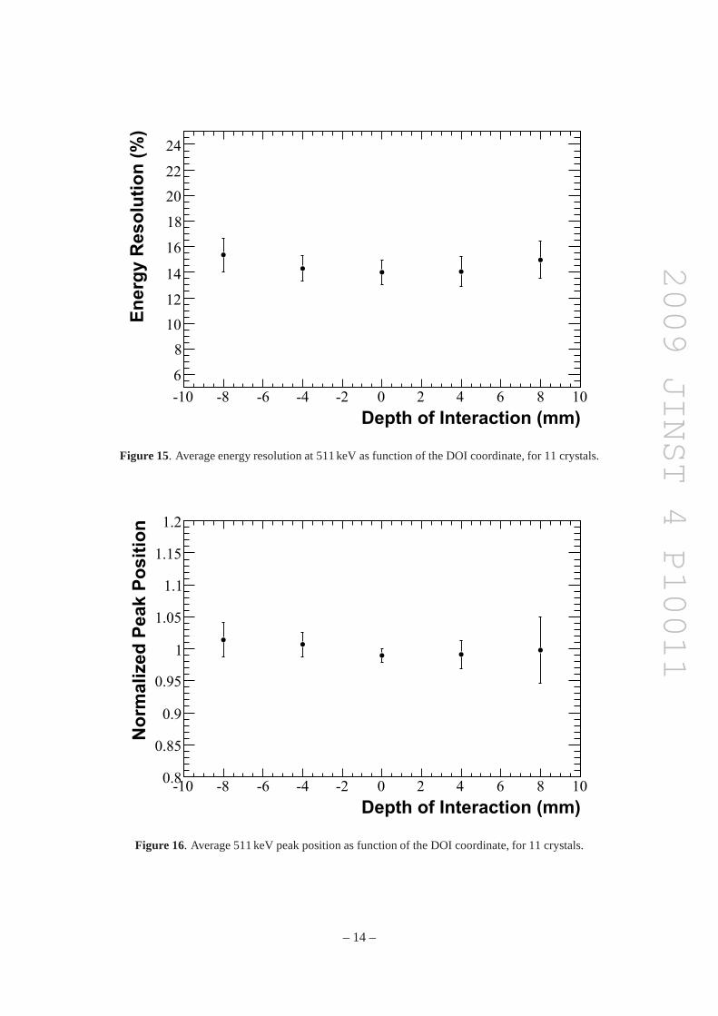
The influence of the DOI of the detected photons on the energy resolution was investigatedby dividing the crystals in five 4 mm bins along the longitudinal axis and analyzing the resultingspectra’s energy resolution. The data for eleven crystals is shown in figure15. The average energyresolution of the full spectra of the analysed crystals is of15.4%. The DOI bins have a higher andmore disperse mean energy resolution value the farther awaythe events’ DOI coordinate is from thecrystal center. For all the analyzed crystals, the full crystal spectrum’s energy resolution is worsethan at least three of the five 4 mm bins spectra’s energy resolution. This can be justified by a slight
– 12 –
2009 JINST 4 P10011
RelK
0.4 0.6 0.8 1 1.2 1.4 1.6
Nu
mb
er
of
Cry
sta
ls
0
200
400
600
800
1000
1200
1400Mean=1.02Dispersion=12.2%
(a)
(keV/ADC Channel)abs
K1 1.5 2 2.5 3 3.5 4
Nu
mb
er
of
Cry
sta
ls
0
200
400
600
800
1000
1200
Mean=2.3Dispersion=15.3%
(b)
(%/mm)DOI
-1C
3 4 5 6 7 8 9
Nu
mb
er
of
Cry
sta
ls
0
200
400
600
800
1000
1200
1400
Mean=5.9Dispersion=7.8%
(c)
Energy Resolution (%)
0.12 0.14 0.16 0.18 0.2
Nu
mb
er
of
Cry
sta
ls
0
200
400
600
800
1000Mean=15.9%Dispersion=8.8%
(d)
Figure 14. Kabs(a),Krel (b),C−1DOI (c), and energy resolution at 511 keV (d) as function of the channel.
variation of the 511 keV peak position with the DOI, which canbe observed in figure16 that showsthe 511 keV peak position (normalized to the average peak position), determined by using ROOT’sSearch algorithm [29], as a function of the DOI coordinate, where the maximum relative variationof the peak position is of 1.4%.
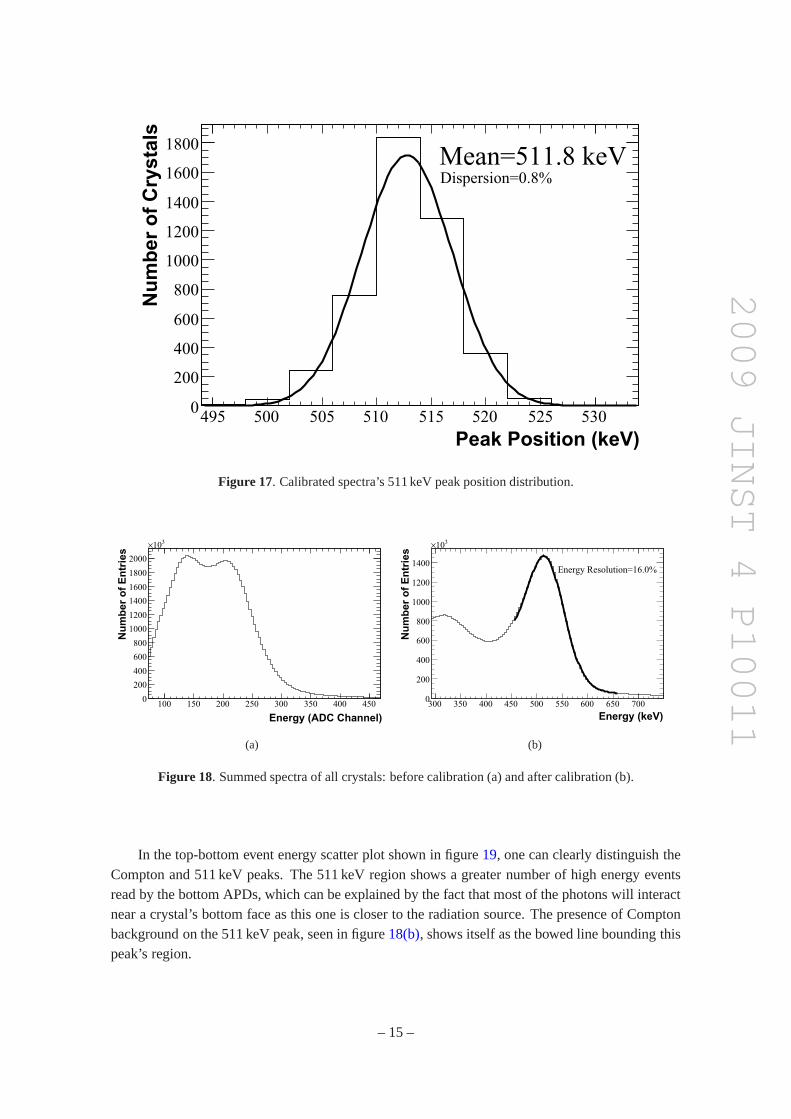
Figure17 shows the distribution of the 511 keV peak position of the calibrated spectra, againdetermined by using ROOT’s Search algorithm [29]. The mean value of the peak’s position, ex-tracted from a gaussian fit, is 511.8 keV with a dispersion of 0.8%, confirming the overall calibra-tion quality and the absolute gain calibration’s validity in particular.
The sum of the spectra of all crystals, before and after the detector’s calibration, are shown,respectively, in figure18(a)and figure18(b). It is difficult to identify the 511 keV peak from thesummed uncalibrated spectra plot, but this peak is clearly recognizable on the summed calibratedspectra plot. Adding the fact that the energy resolution at 511 keV of the summed calibrated spec-tra is 16.0%, being very close to the mean value of the energy resolution distribution showed infigure 14(d), the validity of the calibration performed is again confirmed. One can also concludethat the despite the double-readout configuration decreases the ammount of collected light, it ispossible to obtain an energy resolution similar or better than those obtained with single-readoutschemes with multi-anode PMTs or multi-pixel APDs systems [21, 24, 26].
– 13 –
2009 JINST 4 P10011
Depth of Interaction (mm)
-10 -8 -6 -4 -2 0 2 4 6 8 10
En
erg
y R
eso
luti
on
(%
)
6
8
10
12
14
16
18
20
22
24
Figure 15. Average energy resolution at 511 keV as function of the DOI coordinate, for 11 crystals.
Depth of Interaction (mm)
-10 -8 -6 -4 -2 0 2 4 6 8 10
No
rmalized
Pe
ak P
osit
ion
0.8
0.85
0.9
0.95
1
1.05
1.1
1.15
1.2
Figure 16. Average 511 keV peak position as function of the DOI coordinate, for 11 crystals.
– 14 –
2009 JINST 4 P10011
Peak Position (keV)
495 500 505 510 515 520 525 530
Nu
mb
er
of
Cry
sta
ls
0
200
400
600
800
1000
1200
1400
1600
1800Mean=511.8 keVDispersion=0.8%
Figure 17. Calibrated spectra’s 511 keV peak position distribution.
Energy (ADC Channel)
100 150 200 250 300 350 400 450
Nu
mb
er
of
En
trie
s
0
200
400
600
800
1000
1200
1400
1600
1800
2000
310×
(a)
Energy (keV)
300 350 400 450 500 550 600 650 700
Nu
mb
er
of
En
trie
s
0
200
400
600
800
1000
1200
1400
310×
Energy Resolution=16.0%
(b)
Figure 18. Summed spectra of all crystals: before calibration (a) andafter calibration (b).
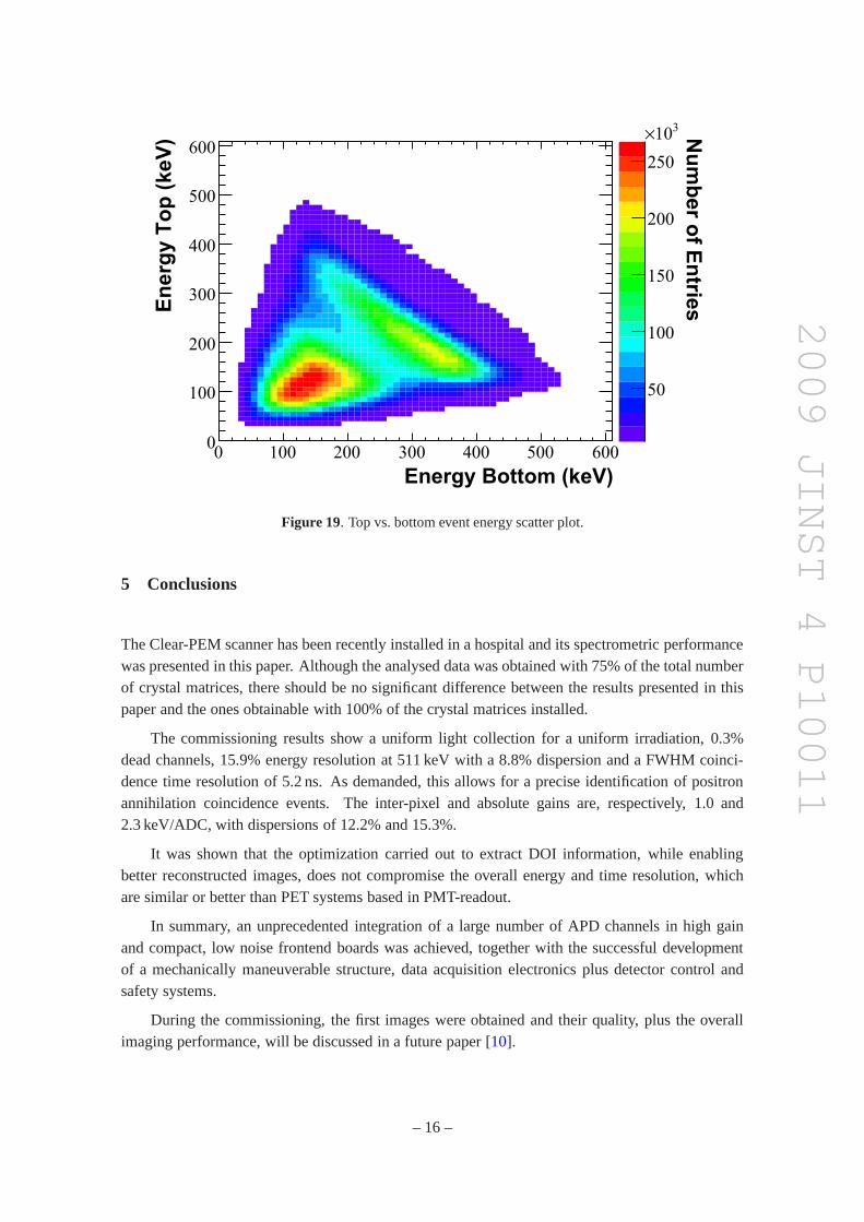
In the top-bottom event energy scatter plot shown in figure19, one can clearly distinguish theCompton and 511 keV peaks. The 511 keV region shows a greater number of high energy eventsread by the bottom APDs, which can be explained by the fact that most of the photons will interactnear a crystal’s bottom face as this one is closer to the radiation source. The presence of Comptonbackground on the 511 keV peak, seen in figure18(b), shows itself as the bowed line bounding thispeak’s region.
– 15 –
2009 JINST 4 P10011
Energy Bottom (keV)
0 100 200 300 400 500 600
En
erg
y T
op
(k
eV
)
0
100
200
300
400
500
600
50
100
150
200
250
310× Nu
mb
er o
f En
tries
Figure 19. Top vs. bottom event energy scatter plot.
5 Conclusions
The Clear-PEM scanner has been recently installed in a hospital and its spectrometric performancewas presented in this paper. Although the analysed data was obtained with 75% of the total numberof crystal matrices, there should be no significant difference between the results presented in thispaper and the ones obtainable with 100% of the crystal matrices installed.
The commissioning results show a uniform light collection for a uniform irradiation, 0.3%dead channels, 15.9% energy resolution at 511 keV with a 8.8%dispersion and a FWHM coinci-dence time resolution of 5.2 ns. As demanded, this allows fora precise identification of positronannihilation coincidence events. The inter-pixel and absolute gains are, respectively, 1.0 and2.3 keV/ADC, with dispersions of 12.2% and 15.3%.
It was shown that the optimization carried out to extract DOIinformation, while enablingbetter reconstructed images, does not compromise the overall energy and time resolution, whichare similar or better than PET systems based in PMT-readout.
In summary, an unprecedented integration of a large number of APD channels in high gainand compact, low noise frontend boards was achieved, together with the successful developmentof a mechanically maneuverable structure, data acquisition electronics plus detector control andsafety systems.
During the commissioning, the first images were obtained andtheir quality, plus the overallimaging performance, will be discussed in a future paper [10].
– 16 –

2009 JINST 4 P10011
Acknowledgments
The authors would like to thank colleagues from the Portuguese PET Consortium and the CrystalClear Collaboration for their suggestions and contribution. The Clear-PEM project is financed byAdI (Agencia de Inovacao) and FCT/POSI (Programa Operacional Sociedade da Informacao), Por-tugal. The work of C. S. Ferreira, P. Rodrigues and A. Trindade was supported by FCT (Fundacaopara a Ciencia e Tecnologia) under grants SFRH/BD/31646/2006, SFRH/BD/47448/2008, SFRH/BPD/37233/2007 and SFRH/BPD/37226/2007. The work of R. Bugalho, B. Carrico, C. Ortigao,J. F. Pinheiro, M. Frade, R. Moura, I. Rolo and R. Silva was supported by AdI.
References
[1] Laco,Sobre o Cancro da Mama, websitehttp://www.laco.pt/layout1.php?p=2(2008).
[2] L. Tafra,Positron Emission Tomography (PET) and Mammography (PEM) for breast cancer:importance to surgeons, Ann. Surg. Oncol.14 (2007) 3.
[3] A. Mavi et al.,Dual Time Point18F-FDG PET Imaging Detects Breast Cancer with High Sensitivityand Correlates Well with Histologic Subtypes, J. Nucl. Med.47 (2006) 1440.
[4] W.W. Moses et al.,PET camera designs for imaging breast cancer and axillary node involvement, J.Nucl. Med.36 (1995) 69P.
[5] C.J. Thompson, K. Murthy , I.N. Weinberg and F.W. Maki,Positron Emission Mammography (PEM):a promising technique to detect breast cancer, IEEE Trans. Nucl. Sci.42 (1995) 1012.
[6] P. Lecoq and J. Varela,Clear PEM, A dedicated PET camera for mammography,Nucl. Instrum. Meth.A 486 (2002) 1.
[7] M.C. Abreu et al.,Design and evaluation of the Clear-PEM scanner for positronemissionmammography, IEEE Trans. Nucl. Sci.53 (2006) 71.
[8] A. Trindade,Design and evaluation of a Positron Emission Tomograph for breast cancer imaging,Ph.D. Thesis, Instituto Superior Tecnico, Portugal (2007).
[9] L. Pidol et al.,High efficiency of lutetium silicate scintillators Ce-doped LPS, and LYSO crystals,IEEE Trans. Nucl. Sci.51 (2004) 1084.
[10] A. Trindade et al.,Study of the influence of depth-of-interaction on Positron Emission Mammographyimages, to be submitted toJINST.
[11] P. Amaral et al.,Performance and quality control of Clear-PEM detector modules,Nucl. Instrum. Meth.A 580 (2007) 1123.
[12] C. Ortigao et al.,Long-term stability of the Clear-PEM detector modules,Nucl. Instrum. Meth.A 571 (2007) 488.
[13] E. Albuquerque et al.,The Clear-PEM electronics system, IEEE Trans. Nucl. Sci.53 (2006) 2704.
[14] M. Martins,3D Image Reconstruction for a Dual Plate Positron Emission Tomograph: Application toMammography, Ph.D. Thesis, Universidade de Lisboa, Portugal (2007).
[15] B. Carrico et al.,Characterization and quality control of avalanche photodiode arrays for theClear-PEM detector modules, Nucl. Instrum. Meth.A 576 (2006) 19.
[16] E. Albuquerque et al.,Experimental characterization of the 192 channel Clear-PEM frontend ASICcoupled to a multi-pixel APD readout of LYSO:Ce crystals, Nucl. Instrum. Meth.A 598 (2009) 802.
– 17 –

2009 JINST 4 P10011
[17] J.F. Pinheiro,Development and study of the Detector Control System and calibration software for theClear-PEM Scanner, Master Thesis,Instituto Superior Tecnico, Portugal (2008).
[18] P. Bento et al.,Performance simulation studies of the Clear-PEM DAQ/Trigger system,IEEE Trans. Nucl. Sci.53 (2006) 2102.
[19] M.C. Abreu et al.,First experimental results with the Clear-PEM detector, in proceedings of2005IEEE Nuclear Science Symposium and Medical Imaging Conference, San Juan Puerto Rico, October23–29 2005,IEEE Nucl. Sci. Symp. Conf. Rec.3 (2005) 5.
[20] G.-C. Wang, J.S. Huber, W.W. Moses, W.-S. Choong and J.S. Maltz,Calibration of a PEM detectorwith depth-of-interaction measurement, IEEE Trans. Nucl. Sci.51 (2004) 775.
[21] G.-C. Wang, J.S. Huber, W.W. Moses, J. Qi and W.-S. Choong, Characterization of the LBNL PEMCamera, IEEE Trans. Nucl. Sci.53 (2006) 1129.
[22] P. Rodrigues,Study and development of the Clear-PEM trigger and data acquisition system, Ph.D.Thesis, Instituto Superior Tecnico, Portugal (2007).
[23] CMS collaboration, P. Busson,Digital Filtering for ECAL trigger primitives generator,CMS-NOTE-1999-020(1999).
[24] P.S. Roldan et al.,Performance evaluation of Raytest ClearPET, a PET scanner for small andmedium size animals, in proceedings of2007 IEEE Nuclear Science Symposium and MedicalImaging Conference, Honolulu Hawaii, U.S.A., October 27 – November 3 2007,IEEE Nucl. Sci. Symp. Conf. Rec.4 (2007) 2859.
[25] M. Bergeron et al.,Performance evaluation of the LabPET APD-based digital PETscanner,IEEE Trans. Nucl. Sci.56 (2009) 10.
[26] D.P. McElroy et al.,Characterization and readout of MADPET-II detector modules: validation of aunique design concept for high resolution Small Animal PET, IEEE Trans. Nucl. Sci.55 (2005) 199.
[27] F. Brun and F. Rademakers,ROOT: An object-oriented data analysis framework,Nucl. Instrum. Meth.389 (1997) 81[Linux J.51 (1998)].
[28] M. Morhac, J. Kliman, V. Matousek, M. Veselsky and I. Turzo,Background elimination methods formultidimensional coincidenceγ-ray spectra, Nucl. Instrum. Meth.A 401 (1997) 113.
[29] M. Morhac et al.,Identification of peaks in multidimensional coincidence gamma-ray spectra,Nucl. Instrum. Meth.A 443 (2000) 108.
– 18 –