Embed Size (px)
Citation preview
1SpgpethtcmtcbpaevpLnandv
tts(ppetto(
1416 J. Opt. Soc. Am. B/Vol. 24, No. 6 /June 2007 Roussey et al.
Experimental and theoretical observationsof the slow-light effect on a tunable
photonic crystal
Matthieu Roussey, Fadi I. Baida, and Maria-Pilar Bernal
Département d’Optique P.M. Duffieux, Institut FEMTO–ST, 16 Route de Gray, 25030 Besançon, France
Received July 24, 2006; revised December 18, 2006; accepted January 25, 2007;posted February 1, 2007 (Doc. ID 73327); published May 17, 2007
We describe how the susceptibility of a nonlinear material, such as lithium niobate, can change when the ma-terial is nanostructured. Indeed, we show, by the calculation of the local-field factor inside a photonic crystal,a significant augmentation of the susceptibility, especially at the edges of the photonic bandgap. In addition,and for the case of lithium niobate, we observe an increase of the second-order nonlinear coefficient. The ex-perimental realization of an electro-optic tunable photonic crystal, based on a square lattice of holes, showsthat the measured phenomenon completely agrees with the theoretical predictions. © 2007 Optical Society ofAmerica
OCIS codes: 250.5300, 250.3140, 230.3990, 190.4390.
te
2Tsdscsprpt
bteddfsdmb
goHtagti
o
. INTRODUCTIONince their discovery in 1987 by Yablonovitch and John,1,2
hotonic crystals (PhCs) have motivated many researchroups and nanophotonics has appeared as a tool with theotential to create optical components as small as theirlectronic counterparts. Up to now, the size of conven-ional tunable optical components (modulators, filters,…)as been of the order of 1 cm. By using PhCs, the size ofhese devices can potentially be reduced to a few mi-rometers. However, the ultimate goal of PhCs is not onlyiniaturization. Indeed, when a material is nanostruc-
ured, its physical properties can be completelyhanged,3,4 and, in particular, its second-order suscepti-ility can increase in the structured area.5–8 In previousapers,9–11 we have chosen lithium niobate (LN) as a suit-ble active material to realize PhCs because of its largelectro-optic and acousto-optic coefficients. We have pre-iously demonstrated what we believe to be the first ex-erimental characterization of a photonic bandgap in aN PhC.10 Recently we have shown12 that an extraordi-ary shift of the photonic bandgap can be observed whenn external voltage is applied on the PhC, but no expla-ation of this phenomenon was given. A more completeescription of the behavior of the light inside the PhC de-ice is reported here.
In this paper, we first present theoretical results ob-ained by FDTD (finite-difference time-domain) simula-ions of a square lattice of holes milled into a LN sub-trate. We study the influence of geometrical parametersthe number of rows of holes and the ratio of radius overeriod) on the transmission. Second, we theoretically ex-lain how the nanostructuring of the bulk material influ-nces the behavior of light and how this can be exploitedo make a low-voltage tunable PhC. Finally, we comparehese theoretical predictions with the experimental dem-nstration of these phenomena and find good agreement2.5 nm/V experimentally observed versus 2.7 nm/V
0740-3224/07/061416-7/$15.00 © 2
heoretically predicted), thus validating our theoreticalxplanation.
. NUMERICAL STUDYhe aim of this section is to describe the studied photonictructures and the FDTD simulations13 carried out in or-er to determine the suitable PhC configuration. Thetructure consists of a square lattice (period a) of cylindri-al air holes (n=1, radius �) etched into an X-cut LN sub-trate �n=2.143�. The incident beam is a plane waveropagating perpendicularly to the hole axis in the �X di-ection of the PhC (Fig. 1). The illuminating light is TEolarized, meaning that the electric field is perpendicularo the axis of the holes.
For the numerical simulations, the structure is definedy its spatial permitivity distribution. An orthogonal Car-esian mesh is usually used, and the resulting staircaseffect typically leads to parasitic diffractive nodes. To re-uce this artifact, two modifications have been intro-uced. The first is based on the introduction of a nonuni-orm mesh in the code. This mesh allows us to change thepatial step in order to describe more accurately the fineetails of the structure. Indeed, inside the PhC a fineesh is applied ��y=18.683 nm�, and outside the PhC a
igger spatial step is used ��y=35 nm�.The second modification involves the use of a staggered
rid.14 The conventional cell, corresponding to one periodf the PhC, would be defined by a grid of 41�41 points.owever, this is not sufficient to have good hole defini-
ion. Thus, each point of the previous grid is considered ascell of 20�20 points, and the dielectric constant of the
rid point is taken to be the average dielectric value overhe 20�20 points of this subgrid. Consequently, the PhCs better defined without increasing the calculation time.
Simulations are made with a single row of holes peri-dically repeated in the Z direction (perpendicular to the
007 Optical Society of America
pfifitmttfe
taooogigtbI
s
tsfilpamb==tpo
tihqnwtFp
tm
Fl�
Fot
Roussey et al. Vol. 24, No. 6 /June 2007/J. Opt. Soc. Am. B 1417
ropagation direction), meaning that the structure is in-nite in this direction. In the propagation direction Y, anite number of holes are introduced at periodicity a, andhe structure is terminated by Berenger’s perfectlyatched layers (PML). To avoid parasitic signals due to
he reflections of evanescent waves from the PML regions,hese layers are placed at a distance larger than �max /2rom the outer holes of the structure (�max being the larg-st wavelength in the studied spectral area).
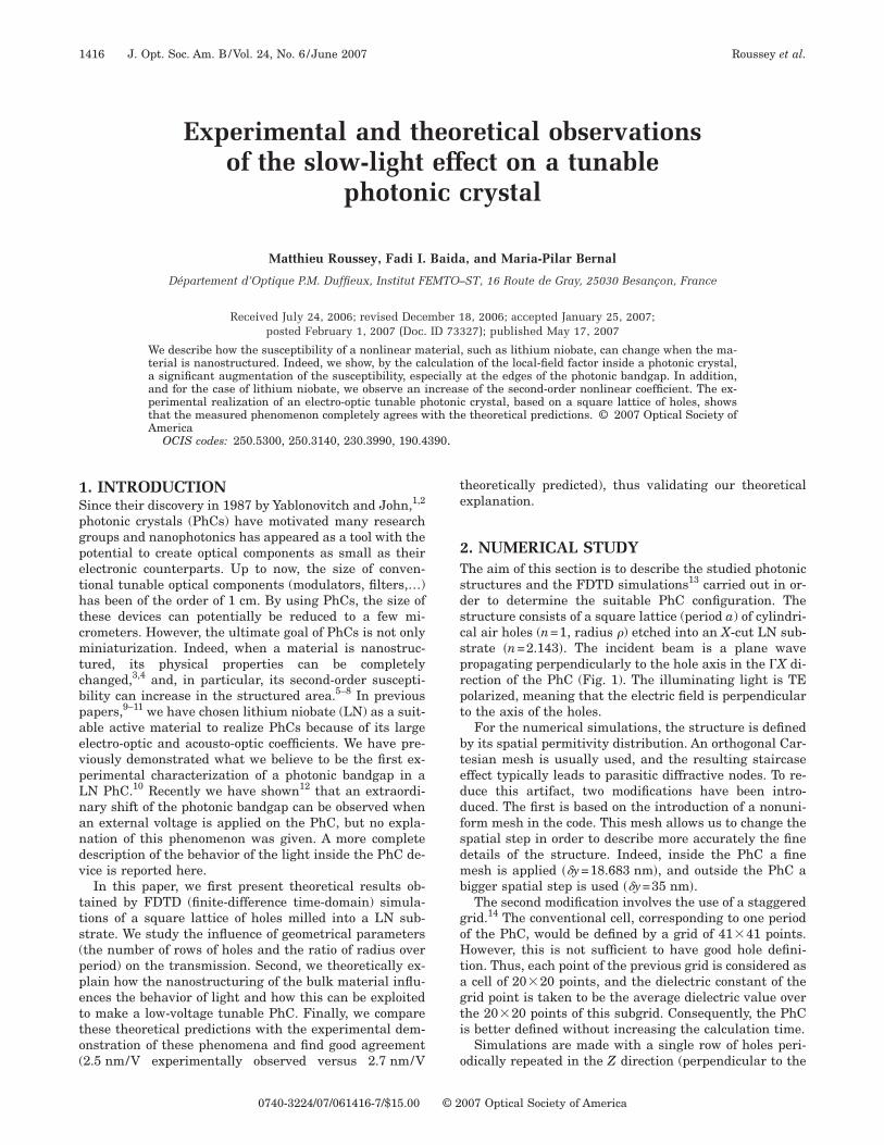
Figure 2 presents the calculated transmission spec-rum through a PhC of 15 rows for a period a=766 nmnd a ratio � /a=0.27. Two gaps can be observed: The firstne is between �=1130 nm and �=1210 nm, and the sec-nd one is between �=1390 nm and �=1550 nm. We canbserve a transmission peak in the middle of the secondap with a maximum intensity at �=1460 nm. The qual-ty factor Q of the peak is equal to 200. This peak is ofreat interest in our case. Indeed, for the fabrication ofunable PhCs, it is easier to obtain a good extinction ratioy tuning a thin peak rather than an edge of the bandgap.n what follows we investigate the origin of this peak.
Figure 3(a) shows the evolution of the transmissionpectrum versus the ratio � /a (abscissa corresponds to
Fig. 1. Scheme of the numerically studied structure.
ig. 2. (Color online) Theoretical transmission spectrum calcu-ated by FDTD in the case of a LN PhC (15 hole rows, n=2.143,=207 nm, a=766 nm, TE polarization).
he wavelength, and the transmitted intensity is pre-ented in gray scale). Within this region, we can observeve bandgaps and an isolated transmission peak, which is
ocated in the highest bandgap. When � /a increases, theeak moves toward shorter wavelengths but remains inll cases in the same bandgap. By choosing suitable geo-etrical parameters, we can set the peak wavelength to
e in the middle of the bandgap. Consequently, for a766 nm and � /a=0.27 the peak is located at �1460 nm, corresponding to a desirable position for fu-
ure experimental characterization (both edges of thehotonic bandgap would be accessible with a conventionalptical spectrum analyzer).
For the parameters noted above, we calculate theransmission spectrum of the PhC in the vicinity of thesolated transmission peak as a function of the number ofole rows. As shown in Fig. 3(b), the position and theuality factor of the transmission peak depend on theumber of hole rows. One also notes that the peak getsider when the number of rows increases. We can remark
hat in the case of a PhC of 15 hole rows [dashed line inig. 3(b)], a good compomise between the thickness of theeak and its intensity has been found.This dependence on the length of the PhC suggests that
he isolated transmission peak is actually a thin trans-ission band separating two photonic bandgaps. Owing
ig. 3. (Color online) (a) Two-dimensional map of the evolutionf the transmission spectrum versus � /a. (b) Close-up around thehin transmission peak versus the number of rows.
twm
rrhcftcctola=tiHwpt
3FIrla
Ipp�
wvt
fiKmt
TfibwhtTtr
msspsm
bfsc
TreEikcettcm
Ifiw
wvob(tfir
Fst(
1418 J. Opt. Soc. Am. B/Vol. 24, No. 6 /June 2007 Roussey et al.
o the Fabry–Perot cavity created by the finite structure,e can, in fact, observe a group of peaks inside this trans-ission band.To take into account the artifacts introduced by the fab-
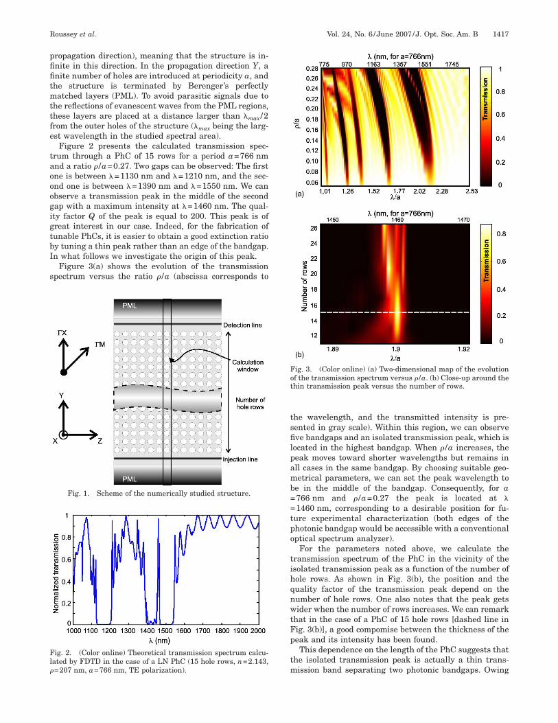
ication process, we have included in our calculations aandom uncertainty in the shape and location of theoles. Experimentally, holes are milled with a FIB (fo-used ion beam)9 that has a resolution of 70 nm. There-ore, in our simulations, we randomly vary the value ofhe period a=a0±�a with a0=766 nm and �a=37 nm. Wean observe in Fig. 4 that this level of fabrication erroran cause the peak to disappear completely and to shifthe bandgap toward lower wavelengths with a decrease inverall transmission. We have performed additional simu-ations (not presented here) with a smaller �a=10 nmnd also with a radius variation (�=�0±��, with �0207 �m and ��=�0 /10), and we observe that in all cases
he peak disappears. Consequently, we can conclude thatt will be difficult to experimentally observe this peak.owever, in the rest of the simulations, the structuresill be considered as perfect ��a=��=0� in order to sim-lify the numerical simulations and the interpretation ofhe results.
. SLOW LIGHT AND LOCAL-FIELDACTOR
n the presence of an external voltage, a nonlinear mate-ial presents a variation of its refractive index [Eq. (1)],inked mainly to the Pockels ��nP� and Kerr ��nK� effects,s
�n = �nP + �nK. �1�
f this variation is linear with the applied field, i.e., de-endent on the second-order susceptibility ��2�, we are inresence of the Pockels effect and the index of variation�nP� is generally calculated as
�nP = −1
2� n3 � r33 �
U
e, �2�
here r33 is the electro-optic coefficient, U is the appliedoltage, e is the distance between the electrodes, and n ishe refractive index.
ig. 4. (Color online) Theoretical transmission (solid curve)pectrum through a perfect square-lattice PhC compared withhe spectrum obtained with a random variation of the period�a=37 nm, black dashed curve).
If the variation depends on the square of the appliedeld, i.e., the third-order susceptibility ��3�, it is called theerr effect. In the case of LN, which is a noncentrosy-etrical material, the Kerr effect is much smaller than
he Pockels effect, and so Eq. (1) can be written as
�n � �nP. �3�
o have the largest electro-optic effect, the following con-guration has been chosen: A PhC (15�15 holes) haseen fabricated on an APE (annealed proton exchange)aveguide parallel to the Y axis of the LN substrate. Theoles have been milled along the X axis, and two elec-rodes have been placed on each side of the waveguide.his means that the electrostatic field lines are parallel to
he Z axis, allowing the largest electro-optic coefficient,33, to be used.
Our experimental results indicate that while Eq. (2)ay apply to a bulk material, we must additionally con-
ider the effect on the susceptibility induced by the nano-tructuring. Indeed, we find theoretically and validate ex-erimentally that this nanostructuring enhances theusceptibility of the material compared with the sameaterial without holes.The effective susceptibility in a structured material has
een previously shown to depend on the local-field factor. Following the approach of Refs. 7 and 15, the effectiveecond-order susceptibility can be related to the bulk sus-eptibility as
�PhC�2� = f3 � �BULK
�2� . �4�
he local-field factor f is equal to 1 outside the bandgap,ecovering the properties of the bulk material, and isqual to 0 inside the bandgap. Because of the change fromq. (2) to Eq. (4), the Pockels equation has to be modified
n order to take this local-field factor into account. Wenow that the second-order susceptibility in the PhC willhange with f3. In our calculations, the following hypoth-sis will be made: We consider that r33d33, where d33 ishe element of the susceptibility tensor. This approxima-ion will be validated by our experimental results. In thisase, the electro-optic coefficient becomes r33� f3 and theodified Pockels equation can be expressed as
�n = −1
2� n3 � r33 � f3 �
U
e. �5�
n the remainder of this section, we calculate the local-eld factor f with two different methods. First, f can beritten as15
f =�vgBULK
vgPhC , �6�
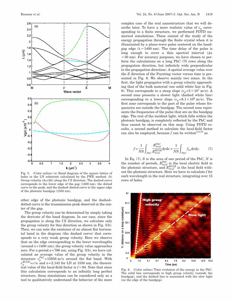
here vgBULK is the group velocity inside the bulk LN and
gPhC is the group velocity in the PhC. The band diagramf the infinite PhC is presented in Fig. 5(a), as computedy a homemade code based on the plane-wave expansionPWE) method. To simplify the comparison with theransmission spectrum shown in Fig. 2, we have used dif-erent symbols for some bands of the diagram correspond-ng to the large bandgap in Fig. 3. The dashed curve cor-esponds to the lower band edge, the dotted curve to the
odt
tptTtst(zcsvitst
cssmeigl�fpttsfii6scfiqseptsc
ttoer
FhGcco
FTb(
Roussey et al. Vol. 24, No. 6 /June 2007/J. Opt. Soc. Am. B 1419
ther edge of the photonic bandgap, and the dashed–otted curve is the transmission peak observed in the cen-er of the gap.
The group velocity can be determined by simply takinghe derivate of the band diagram. In our case, since theropagation is along the �X direction, we calculate onlyhe group velocity for this direction as shown in Fig. 5(b).hen, we can note the existence of an almost flat horizon-al band in the diagram (the dashed curve) that corre-ponds to a very weak group velocity. Here we observehat on the edge corresponding to the lower wavelengthsaround �=1400 nm), the group velocity value approachesero. For a period a=766 nm, using Fig. 5(b), we have cal-ulated an average value of the group velocity in thetructure vg
PhC=15858 m/s around the flat band. With
gBULK=c /n and n=2.143 for LN at 1550 nm, the theoret-cal value of the local-field factor is f�94. Note that sincehis calculation corresponds to an infinitly long perfecttructure, these simulations can be considered only as aool to qualitatively understand the behavior of the more
ig. 5. (Color online) (a) Band diagram of the square lattice ofoles in the LN substrate calculated by the PWE method. (b)roup velocity �d /dk� along the �X direction. The dashed curve
orresponds to the lower edge of the gap �1400 nm�, the dottedurve to the peak, and the dashed–dotted curve to the upper edgef the photonic bandgap �1550 nm�.
omplex case of the real nanostructure that we will de-cribe later. To have a more realistic value of vg corre-ponding to a finite structure, we performed FDTD nu-erical simulations. These consist of the study of the
nergy propagation through the finite crystal when it islluminated by a plane-wave pulse centered on the band-ap edge ���1400 nm�. The time delay of the pulse isong enough to cover a thin spectral interval ���
30 nm�. For accuracy purposes, we have chosen to per-orm the calculations on a long PhC (75 rows along theropagation direction, but infinitely wide perpendicularo the propagation direction). A spatial average value overhe Z direction of the Poynting vector versus time is pre-ented in Fig. 6. We observe mainly two zones. In therst, the light propagates with a group velocity approach-
ng that of the bulk material (see solid white line in Fig.). This corresponds to a steep slope �vg=5�107 m/s�. Aecond zone presents a slower light (dashed white line)orresponding to a lower slope �vg=6.1�106 m/s�. Therst zone corresponds to the part of the pulse whose fre-uencies are outside the bandgap. The second zone repre-ents the frequencies of the pulse that are on the bandgapdge. The rest of the incident light, which falls within thehotonic bandgap, is completely reflected by the PhC andhus cannot be observed on this map. Using FDTD re-ults, a second method to calculate the local-field factoran also be employed, because f can be written3,4,15 as
f =1
NS�PhC
ElocalPhC
ElocalBULKdydz =
1
NS�PhC
flocdxdy. �7�
In Eq. (7), S is the area of one period of the PhC, N ishe number of periods, Elocal
PhC is the local electric field inhe photonic structure, and Elocal
BULK is the local field with-ut the photonic structure. Here we have to calculate f forach wavelength in the real structure, integrating over 15ows of holes.
ig. 6. (Color online) Time evolution of the energy in the PhC.he solid line corresponds to high group velocity (outside theandgap), and the dashed line is associated with the slow lighton the edge of the bandgap).
aFFfaFfaiae
vg(lptfitd
=
tm
4ItsspmhpteliPsfistbcdv
taFsAmlfi=
f8tpntlo
aw
Fotvt
1420 J. Opt. Soc. Am. B/Vol. 24, No. 6 /June 2007 Roussey et al.
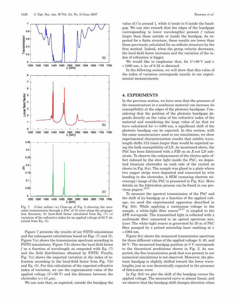
Figure 7 presents the results of our FDTD simulationsnd the subsequent calculations based on Eqs. (7) and (5).igure 7(a) shows the transmission spectrum according toDTD simulations. Figure 7(b) shows the local-field factoras a function of wavelength as computed with Eq. (7)nd the field distributions obtained by FDTD. Finally,ig. 7(c) shows the expected variation in the index of re-
raction according to the local-field factor from Fig. 7(b)nd Eq. (5). For this calculation of the expected refractivendex of variation, we use the experimental value of thepplied voltage �U=80 V� and the distance between thelectrodes �e=13 �m�.
We can note that, as expected, outside the bandgap the
ig. 7. (Color online) (a) Close-up of Fig. 2 showing the zero-rder transmission through a PhC of 15 rows along the propaga-ion direction; (b) local-field factor calculated from Eq. (7); (c)ariation of the refractive index for an applied voltage of 80 V ob-ained from Eq. (5).
alue of f is around 1, while it tends to 0 inside the band-ap. We can also remark that the edges of the bandgapscorresponding to lower wavelengths) present f valuesarger than those outside or inside the bandgap. As ex-ected for a finite structure, these results are lower thanhose previously calculated for an infinite structure by therst method. Indeed, when the group velocity decreases,he local-field factor increases and the variation of the in-ex of refraction is bigger.We would like to emphasize that, for U=80 V and �
1400 nm, a �n of 0.32 is obtained.In the following section, we will show that this value of
he index of variation corresponds exactly to our experi-ental measurements.
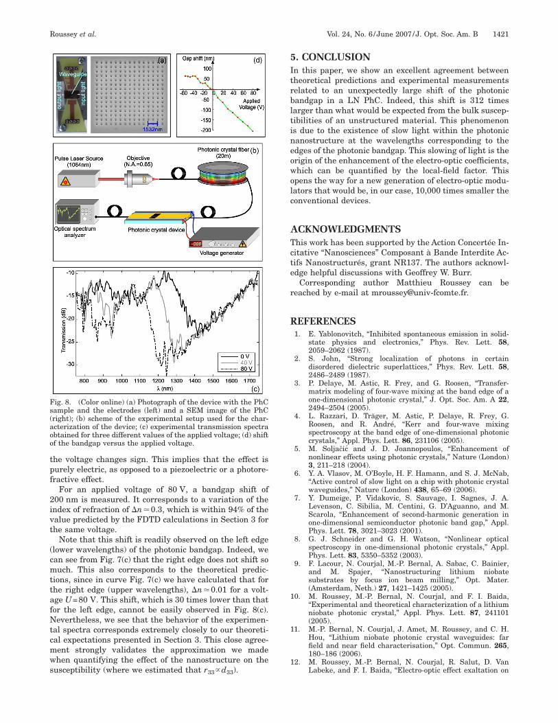
. EXPERIMENTSn the previous section, we have seen that the presence ofhe nanostructure in a nonlinear material can increase itsusceptibility at the edges of the photonic bandgaps. Con-idering that the position of the photonic bandgaps de-ends directly on the value of the refractive index of theaterial and considering the large value of �n that weave calculated for �=1400 nm, a significant shift of thehotonic bandgap can be expected. In this section, withhe same nanostructure used in our simulations, we showxperimental characterization results that exhibit wave-ength shifts 312 times larger than would be expected us-ng the bulk susceptibility of LN. As mentioned above, thehC has been fabricated with a FIB on an X-cut LN sub-trate. To observe the enhancement of the electro-optic ef-ect induced by the slow light inside the PhC, we depos-ted titanium electrodes on each side of the crystal ashown in Fig. 8(a). The sample was glued to a plate wherewo copper strips were deposited and connected by wireonding to the electrodes. A SEM (scanning electron mi-roscopy) image of the PhC is presented in Fig. 8(a). Moreetails on the fabrication process can be found in our pre-ious papers.10,11
To measure the spectral transmission of the PhC andhe shift of its bandgap as a function of the applied volt-ge, we used the experimental apparatus described inig. 8(b). While applying a continuous voltage to theample, a white-light fiber source16,17 is coupled to thePE waveguide. The transmitted light is collected with aultimode fiber connected to an optical spectrum ana-
yzer. The white-light source is generated by 20 m of PhCber pumped by a pulsed microchip laser emitting at �1064 nm.Figure 8(c) shows the measured transmission spectrum
or three different values of the applied voltage: 0, 40, and0 V. The measured bandgap position at 0 V correspondso the theoretical predictions shown in Fig. 2. As sus-ected, the fine transmission peak that was present in ourumerical simulations is not observed. Moreover, the pho-onic bandgap is slightly shifted toward the lower wave-engths just as was theoretically expected in the presencef fabrication error.
In Fig. 8(d) we plot the shift of the bandgap versus thepplied voltage. The measured curve is almost linear, ande observe that the bandgap shift changes direction when
tpf
2ivt
(cmttafNtcmws
5Itrbltineowolc
ATcte
r
R
1
1
1
Fs(aoo
Roussey et al. Vol. 24, No. 6 /June 2007/J. Opt. Soc. Am. B 1421
he voltage changes sign. This implies that the effect isurely electric, as opposed to a piezoelectric or a photore-ractive effect.
For an applied voltage of 80 V, a bandgap shift of00 nm is measured. It corresponds to a variation of thendex of refraction of �n�0.3, which is within 94% of thealue predicted by the FDTD calculations in Section 3 forhe same voltage.
Note that this shift is readily observed on the left edgelower wavelengths) of the photonic bandgap. Indeed, wean see from Fig. 7(c) that the right edge does not shift souch. This also corresponds to the theoretical predic-
ions, since in curve Fig. 7(c) we have calculated that forhe right edge (upper wavelengths), �n�0.01 for a volt-ge U=80 V. This shift, which is 30 times lower than thator the left edge, cannot be easily observed in Fig. 8(c).evertheless, we see that the behavior of the experimen-
al spectra corresponds extremely closely to our theoreti-al expectations presented in Section 3. This close agree-ent strongly validates the approximation we madehen quantifying the effect of the nanostructure on the
usceptibility (where we estimated that r d ).
ig. 8. (Color online) (a) Photograph of the device with the PhCample and the electrodes (left) and a SEM image of the PhCright); (b) scheme of the experimental setup used for the char-cterization of the device; (c) experimental transmission spectrabtained for three different values of the applied voltage; (d) shiftf the bandgap versus the applied voltage.
33 33
. CONCLUSIONn this paper, we show an excellent agreement betweenheoretical predictions and experimental measurementselated to an unexpectedly large shift of the photonicandgap in a LN PhC. Indeed, this shift is 312 timesarger than what would be expected from the bulk suscep-ibilities of an unstructured material. This phenomenons due to the existence of slow light within the photonicanostructure at the wavelengths corresponding to thedges of the photonic bandgap. This slowing of light is therigin of the enhancement of the electro-optic coefficients,hich can be quantified by the local-field factor. Thispens the way for a new generation of electro-optic modu-ators that would be, in our case, 10,000 times smaller theonventional devices.
CKNOWLEDGMENTShis work has been supported by the Action Concertée In-itative “Nanosciences” Composant à Bande Interdite Ac-ifs Nanostructurés, grant NR137. The authors acknowl-dge helpful discussions with Geoffrey W. Burr.
Corresponding author Matthieu Roussey can beeached by e-mail at [email protected].
EFERENCES1. E. Yablonovitch, “Inhibited spontaneous emission in solid-
state physics and electronics,” Phys. Rev. Lett. 58,2059–2062 (1987).
2. S. John, “Strong localization of photons in certaindisordered dielectric superlattices,” Phys. Rev. Lett. 58,2486–2489 (1987).
3. P. Delaye, M. Astic, R. Frey, and G. Roosen, “Transfer-matrix modeling of four-wave mixing at the band edge of aone-dimensional photonic crystal,” J. Opt. Soc. Am. A 22,2494–2504 (2005).
4. L. Razzari, D. Träger, M. Astic, P. Delaye, R. Frey, G.Roosen, and R. André, “Kerr and four-wave mixingspectroscopy at the band edge of one-dimensional photoniccrystals,” Appl. Phys. Lett. 86, 231106 (2005).
5. M. Soljačic and J. D. Joannopoulos, “Enhancement ofnonlinear effects using photonic crystals,” Nature (London)3, 211–218 (2004).
6. Y. A. Vlasov, M. O’Boyle, H. F. Hamann, and S. J. McNab,“Active control of slow light on a chip with photonic crystalwaveguides,” Nature (London) 438, 65–69 (2006).
7. Y. Dumeige, P. Vidakovic, S. Sauvage, I. Sagnes, J. A.Levenson, C. Sibilia, M. Centini, G. D’Aguanno, and M.Scarola, “Enhancement of second-harmonic generation inone-dimensional semiconductor photonic band gap,” Appl.Phys. Lett. 78, 3021–3023 (2001).
8. G. J. Schneider and G. H. Watson, “Nonlinear opticalspectroscopy in one-dimensional photonic crystals,” Appl.Phys. Lett. 83, 5350–5352 (2003).
9. F. Lacour, N. Courjal, M.-P. Bernal, A. Sabac, C. Bainier,and M. Spajer, “Nanostructuring lithium niobatesubstrates by focus ion beam milling,” Opt. Mater.(Amsterdam, Neth.) 27, 1421–1425 (2005).
0. M. Roussey, M.-P. Bernal, N. Courjal, and F. I. Baida,“Experimental and theoretical characterization of a lithiumniobate photonic crystal,” Appl. Phys. Lett. 87, 241101(2005).
1. M.-P. Bernal, N. Courjal, J. Amet, M. Roussey, and C. H.Hou, “Lithium niobate photonic crystal waveguides: farfield and near field characterisation,” Opt. Commun. 265,180–186 (2006).
2. M. Roussey, M.-P. Bernal, N. Courjal, R. Salut, D. VanLabeke, and F. I. Baida, “Electro-optic effect exaltation on

1
1
1
1
1
1422 J. Opt. Soc. Am. B/Vol. 24, No. 6 /June 2007 Roussey et al.
lithium niobate photonic crystals due to slow photons,”Appl. Phys. Lett. 89, 241110 (2006).
3. A. Taflove and S. C. Hagness, ComputationalElectrodynamics, the Finite-Difference Time-Domain, 2nded (Artech, 2000).
4. C. T. Chan, Q. L. Xu, and K. M. Ho, “Order-N spectralmethod for electromagnetic waves,” Phys. Rev. B 51,16635–16642 (1995).
5. H. Rigneault, J.-M. Lourtioz, C. Delalande, and A.Levensen, La nanophotonique (Lavoisier, 2005).
6. W. Wadsworth, N. Joly, J. Knight, T. Birks, F. Biancalana,and P. Russell, “Supercontinuum and four-wave mixingwith Q-switched pulses in endlessly single-mode photoniccrystal fibers,” Opt. Express 12, 299–309 (2004).
7. A. Mussot, T. Sylvestre, L. Provino, and H. Maillotte,“Generation of a broadband single-mode supercontinuumin a conventional dispersion shifted fiber by use of asubnanosecond microchip laser,” Opt. Lett. 29, 1820–1822(2003).