Embed Size (px)
Citation preview
EIE 312 Electronics Engineering Laboratory
3-1
Experiment Topic: AM Modulator
3.1: Curriculum Objectives
1. To understand the basic theory of amplitude modulation (AM).
2. To understand the waveform and frequency spectrum of AM modulator, also
calculate the percentage of modulation.
3. To design and implement the AM modulator by using transistor.
4. To design and implement the AM modulator by balanced modulator.
5. To understand the measurement and adjustment of AM modulator
3.2: Curriculum Theory
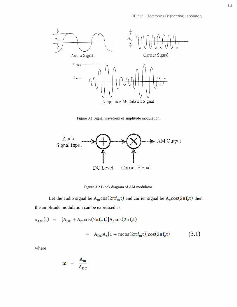
In amplitude modulation (AM), we utilize the amplitude of audio signal to
modulate the amplitude of carrier signal, which means that the amplitude of carrier signal
will be varied with amplitude of audio signal. The waveform of AM modulation is shown
in figure 3.1 and its block diagram is shown in figure 3.2. In figure 3.2, we know that in
order to generate the AM signal, we just need to add a DC signal with the audio signal,
and then multiply the added signal with the carrier signal.
EIE 312 Electronics Engineering Laboratory
3-2
Figure 3.1 Signal waveform of amplitude modulation.
Figure 3.2 Block diagram of AM modulator.
Let the audio signal be and carrier signal be then
the amplitude modulation can be expressed as
(3.1)
where
EIE 312 Electronics Engineering Laboratory
3-3
: DC signal magnitude.
: Audio signal amplitude.
: Carrier signal amplitude.
: Audio signal frequency.
: Carrier signal frequency.
m : Modulation index or depth of modulation.
From equation (3.1), we notice that the variation of the magnitude
of the carrier signal can be controlled by parameter “m”.
This means that we can change the magnitude of the audio signal or DC signal
to control the level or depth of the carrier signal. Therefore, this parameter “m” is
known as the modulation index.
Besides, we can also rewrite equation (3.1) as
(3.2)
The first term represents double sideband signals; the second term represents
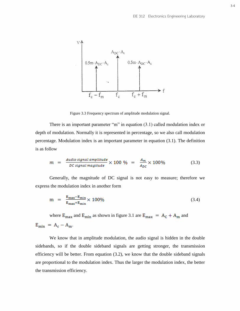
carrier signal. From equation (3.2), we can sketch the frequency spectrum of amplitude
modulation as shown in figure 3.3. Since the audio signal is hidden in the double
sidebands and the carrier signal does not contain any message, therefore the power is
consumed in carrier during transmission of amplitude modulation signal. For this reason,
the transmission efficiency of AM modulation is lower than double sidebands suppressed
carrier (DSB-SC) modulation but its demodulation circuit is much simpler.
EIE 312 Electronics Engineering Laboratory
3-4
Figure 3.3 Frequency spectrum of amplitude modulation signal.
There is an important parameter “m” in equation (3.1) called modulation index or
depth of modulation. Normally it is represented in percentage, so we also call modulation
percentage. Modulation index is an important parameter in equation (3.1). The definition
is as follow
(3.3)
Generally, the magnitude of DC signal is not easy to measure; therefore we
express the modulation index in another form
(3.4)
where and as shown in figure 3.1 are and
.
We know that in amplitude modulation, the audio signal is hidden in the double
sidebands, so if the double sideband signals are getting stronger, the transmission
efficiency will be better. From equation (3.2), we know that the double sideband signals
are proportional to the modulation index. Thus the larger the modulation index, the better
the transmission efficiency.
EIE 312 Electronics Engineering Laboratory
3-5
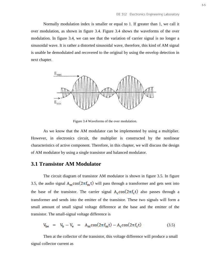
Normally modulation index is smaller or equal to 1. If greater than 1, we call it
over modulation, as shown in figure 3.4. Figure 3.4 shows the waveforms of the over
modulation. In figure 3.4, we can see that the variation of carrier signal is no longer a
sinusoidal wave. It is rather a distorted sinusoidal wave, therefore, this kind of AM signal
is unable be demodulated and recovered to the original by using the envelop detection in
next chapter.
Figure 3.4 Waveforms of the over modulation.
As we know that the AM modulator can be implemented by using a multiplier.
However, in electronics circuit, the multiplier is constructed by the nonlinear
characteristics of active component. Therefore, in this chapter, we will discuss the design
of AM modulator by using a single transistor and balanced modulator.
3.1 Transistor AM Modulator
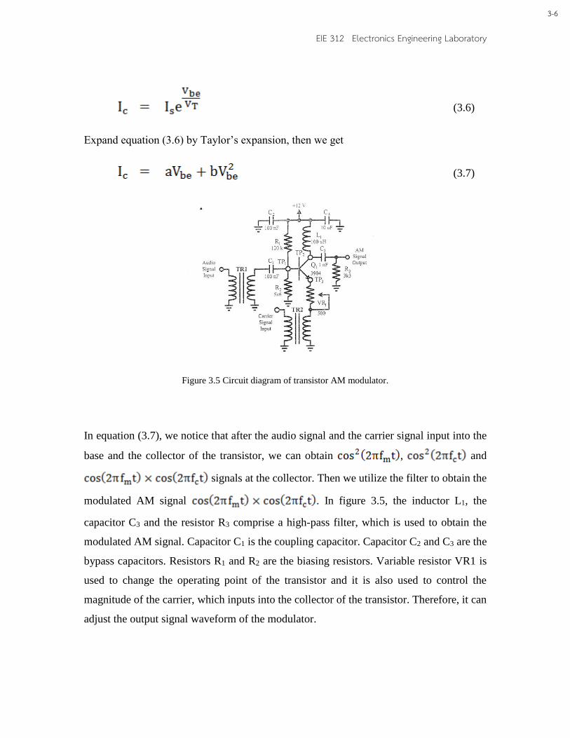
The circuit diagram of transistor AM modulator is shown in figure 3.5. In figure
3.5, the audio signal will pass through a transformer and gets sent into
the base of the transistor. The carrier signal also passes through a
transformer and sends into the emitter of the transistor. These two signals will form a
small amount of small signal voltage difference at the base and the emitter of the
transistor. The small-signal voltage difference is
(3.5)
Then at the collector of the transistor, this voltage difference will produce a small
signal collector current as
EIE 312 Electronics Engineering Laboratory
3-6
(3.6)
Expand equation (3.6) by Taylor’s expansion, then we get
(3.7)
Figure 3.5 Circuit diagram of transistor AM modulator.
In equation (3.7), we notice that after the audio signal and the carrier signal input into the
base and the collector of the transistor, we can obtain , and
signals at the collector. Then we utilize the filter to obtain the
modulated AM signal . In figure 3.5, the inductor L1, the
capacitor C3 and the resistor R3 comprise a high-pass filter, which is used to obtain the
modulated AM signal. Capacitor C1 is the coupling capacitor. Capacitor C2 and C3 are the
bypass capacitors. Resistors R1 and R2 are the biasing resistors. Variable resistor VR1 is
used to change the operating point of the transistor and it is also used to control the
magnitude of the carrier, which inputs into the collector of the transistor. Therefore, it can
adjust the output signal waveform of the modulator.
EIE 312 Electronics Engineering Laboratory
3-7
3.2 MC 1496 AM Modulator
The main difference between the design of AM modulator by using balanced
modulator and the transistor is that we can use the theory of balanced modulator to cancel
out the unwanted harmonics signals, which is produced by the nonlinear characteristic of
the transistor, then the remaining signal is the AM signal. In this chapter, we utilize the
balanced modulator (MC1496) to implement the AM modulator.
Following the variation of input signal frequency, the balanced modulator
(MC1496) can become a frequency multiplier, AM modulator or double sidebands
suppressed carrier modulator (DSB-SC Modulator). Its input signal, output signal and
circuit characteristics show in table 3.1.
Table 3.1 Three different types of modulation signal produced by different signals frequency of balanced
modulator.
Input Carrier
Signal
Input Audio
Signal
Output Balanced
Modulator
Circuit
Characteristics
2 Frequency
Multiplier
,
,
Amplitude
Modulator
, DSB-SC Modulator
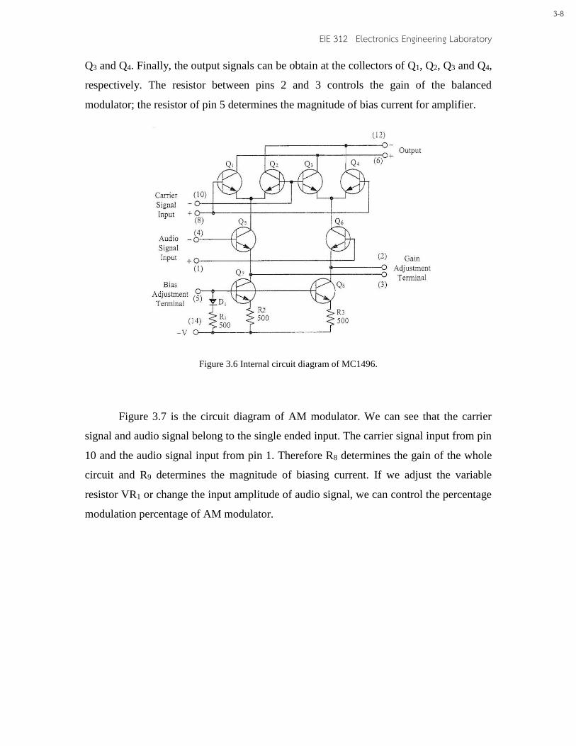
Figure 3.6 is the internal circuit diagram of MC1496, where D1, R1, R2, R3, Q7
and Q8 comprise an electric current source, which can supply DC bias current for Q5 and
Q6. Q5 and Q6 comprise a differential combination to drive the dual differential amplifiers
constructed by Q1, Q2, Q3 and Q4. Pins 1 and 4 are the inputs of audio signal, after that
this signal will be amplified by the differential amplifier, which is comprised of Q5 and
Q6. Pin 8 and 10 are the inputs of carrier signal. Then the amplified audio signal will be
multiplied by the carrier signal at the dual differential amplifiers constructed by Q1, Q2,
EIE 312 Electronics Engineering Laboratory
3-8
Q3 and Q4. Finally, the output signals can be obtain at the collectors of Q1, Q2, Q3 and Q4,
respectively. The resistor between pins 2 and 3 controls the gain of the balanced
modulator; the resistor of pin 5 determines the magnitude of bias current for amplifier.
Figure 3.6 Internal circuit diagram of MC1496.
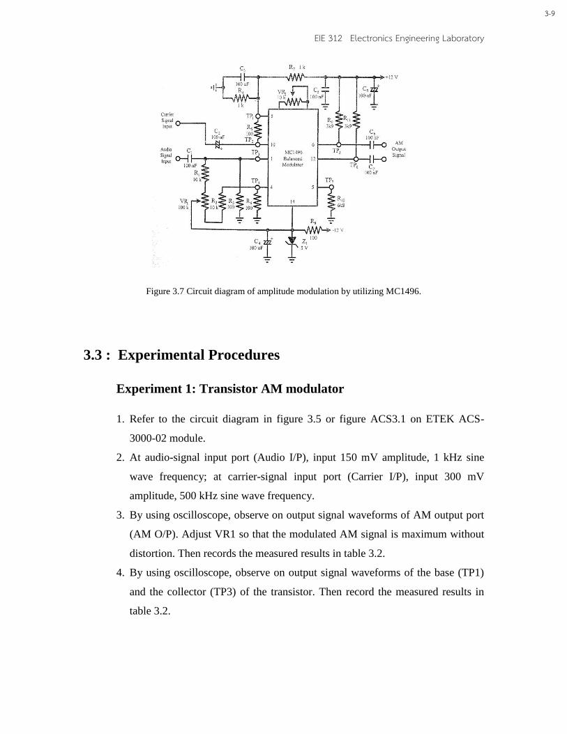
Figure 3.7 is the circuit diagram of AM modulator. We can see that the carrier
signal and audio signal belong to the single ended input. The carrier signal input from pin
10 and the audio signal input from pin 1. Therefore R8 determines the gain of the whole
circuit and R9 determines the magnitude of biasing current. If we adjust the variable
resistor VR1 or change the input amplitude of audio signal, we can control the percentage
modulation percentage of AM modulator.
EIE 312 Electronics Engineering Laboratory
3-9
Figure 3.7 Circuit diagram of amplitude modulation by utilizing MC1496.
3.3 : Experimental Procedures
Experiment 1: Transistor AM modulator
1. Refer to the circuit diagram in figure 3.5 or figure ACS3.1 on ETEK ACS-
3000-02 module.
2. At audio-signal input port (Audio I/P), input 150 mV amplitude, 1 kHz sine
wave frequency; at carrier-signal input port (Carrier I/P), input 300 mV
amplitude, 500 kHz sine wave frequency.
3. By using oscilloscope, observe on output signal waveforms of AM output port
(AM O/P). Adjust VR1 so that the modulated AM signal is maximum without
distortion. Then records the measured results in table 3.2.
4. By using oscilloscope, observe on output signal waveforms of the base (TP1)
and the collector (TP3) of the transistor. Then record the measured results in
table 3.2.
EIE 312 Electronics Engineering Laboratory
3-10
5. By using oscilloscope, observe on signal waveforms of the mixing (TP2) of the
transistor. Then record the measured results in table3.2.
6. By using spectrum analyzer, observe on the frequency spectrum of AM O/P
and TP2. Then record the measured results in table 3.2.
7. Substitute the measured results into equation (3.4), find the modulation
percentage and record in table 3.2.
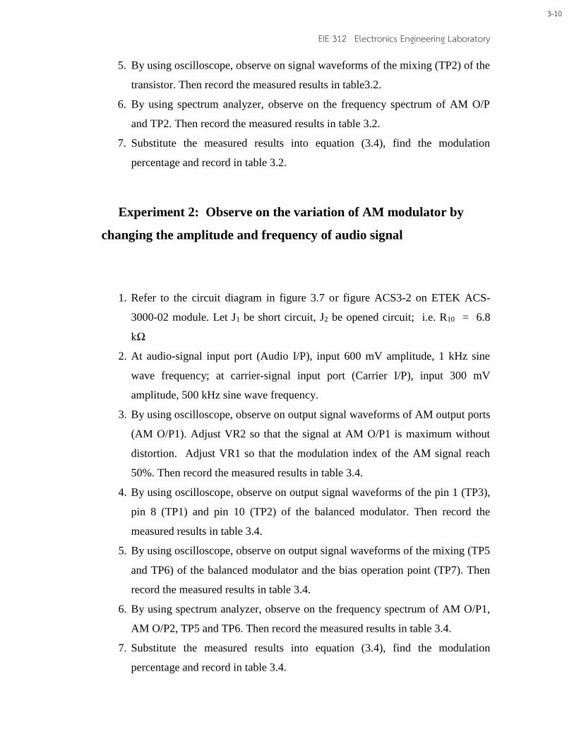
Experiment 2: Observe on the variation of AM modulator by
changing the amplitude and frequency of audio signal
1. Refer to the circuit diagram in figure 3.7 or figure ACS3-2 on ETEK ACS-
3000-02 module. Let J1 be short circuit, J2 be opened circuit; i.e. R10 = 6.8
kΩ
2. At audio-signal input port (Audio I/P), input 600 mV amplitude, 1 kHz sine
wave frequency; at carrier-signal input port (Carrier I/P), input 300 mV
amplitude, 500 kHz sine wave frequency.
3. By using oscilloscope, observe on output signal waveforms of AM output ports
(AM O/P1). Adjust VR2 so that the signal at AM O/P1 is maximum without
distortion. Adjust VR1 so that the modulation index of the AM signal reach
50%. Then record the measured results in table 3.4.
4. By using oscilloscope, observe on output signal waveforms of the pin 1 (TP3),
pin 8 (TP1) and pin 10 (TP2) of the balanced modulator. Then record the
measured results in table 3.4.
5. By using oscilloscope, observe on output signal waveforms of the mixing (TP5
and TP6) of the balanced modulator and the bias operation point (TP7). Then
record the measured results in table 3.4.
6. By using spectrum analyzer, observe on the frequency spectrum of AM O/P1,
AM O/P2, TP5 and TP6. Then record the measured results in table 3.4.
7. Substitute the measured results into equation (3.4), find the modulation
percentage and record in table 3.4.
EIE 312 Electronics Engineering Laboratory
3-11
8. According to the input signals in table 3.4, repeat step 4 to 7 and record the
measured results in table 3.4.
Experiment 3: Variation of AM modulator by changing the
variable resistor VR1
1. Refer to the circuit diagram in figure 3.7 or figure ACS3.2 on ETEK ACS-
3000-02 module. Let J1 be opened circuit, J2 be short circuit; i.e. R12 = 3.3 kΩ
2. At audio-signal input port (Audio I/P), input 600 mV amplitude, 1 kHz sine
wave frequency; at carrier-signal input port (Carrier I/P), input 300 mV
amplitude, 500 kHz sine wave frequency.
3. By using oscilloscope, observe on output signal waveforms of AM output ports
(AM O/P1). Adjust VR1 so that the modulation index of the AM signal reach
30%. Then record the measured results in table 3.9.
4. By using spectrum analyzer, observe on the frequency spectrum of AM O/P1.
Then record the measured results in table 3.9.
5. Substitute the measured results into equation (3.4), find the modulation
percentage and record in table 3.9.
6. According to the modulation index in table 3.9, repeat steps 3 to 5 and record
the measured results in table 3.9.
EIE 312 Electronics Engineering Laboratory
3-12
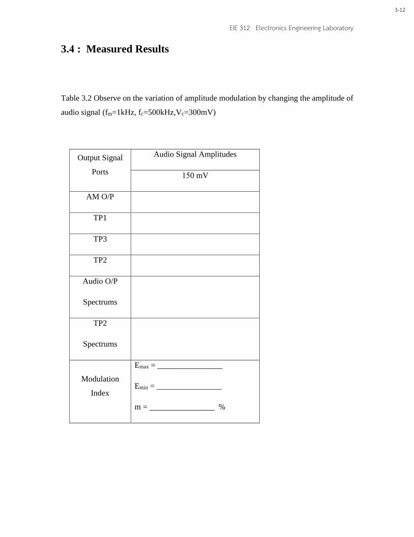
3.4 : Measured Results
Table 3.2 Observe on the variation of amplitude modulation by changing the amplitude of
audio signal (fm=1kHz, fc=500kHz,Vc=300mV)
Output Signal
Ports
Audio Signal Amplitudes
150 mV
AM O/P
TP1
TP3
TP2
Audio O/P
Spectrums
TP2
Spectrums
Modulation
Index
Emax = ________________
Emin = ________________
m = ________________ %
EIE 312 Electronics Engineering Laboratory
3-13
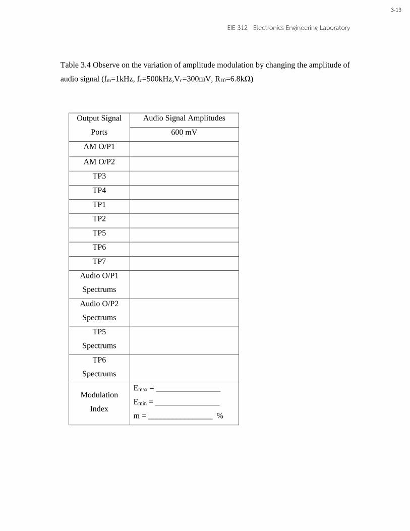
Table 3.4 Observe on the variation of amplitude modulation by changing the amplitude of
audio signal (fm=1kHz, fc=500kHz,Vc=300mV, R10=6.8kΩ)
Output Signal
Ports
Audio Signal Amplitudes
600 mV
AM O/P1
AM O/P2
TP3
TP4
TP1
TP2
TP5
TP6
TP7
Audio O/P1
Spectrums
Audio O/P2
Spectrums
TP5
Spectrums
TP6
Spectrums
Modulation
Index
Emax = ________________
Emin = ________________
m = ________________ %
EIE 312 Electronics Engineering Laboratory
3-14
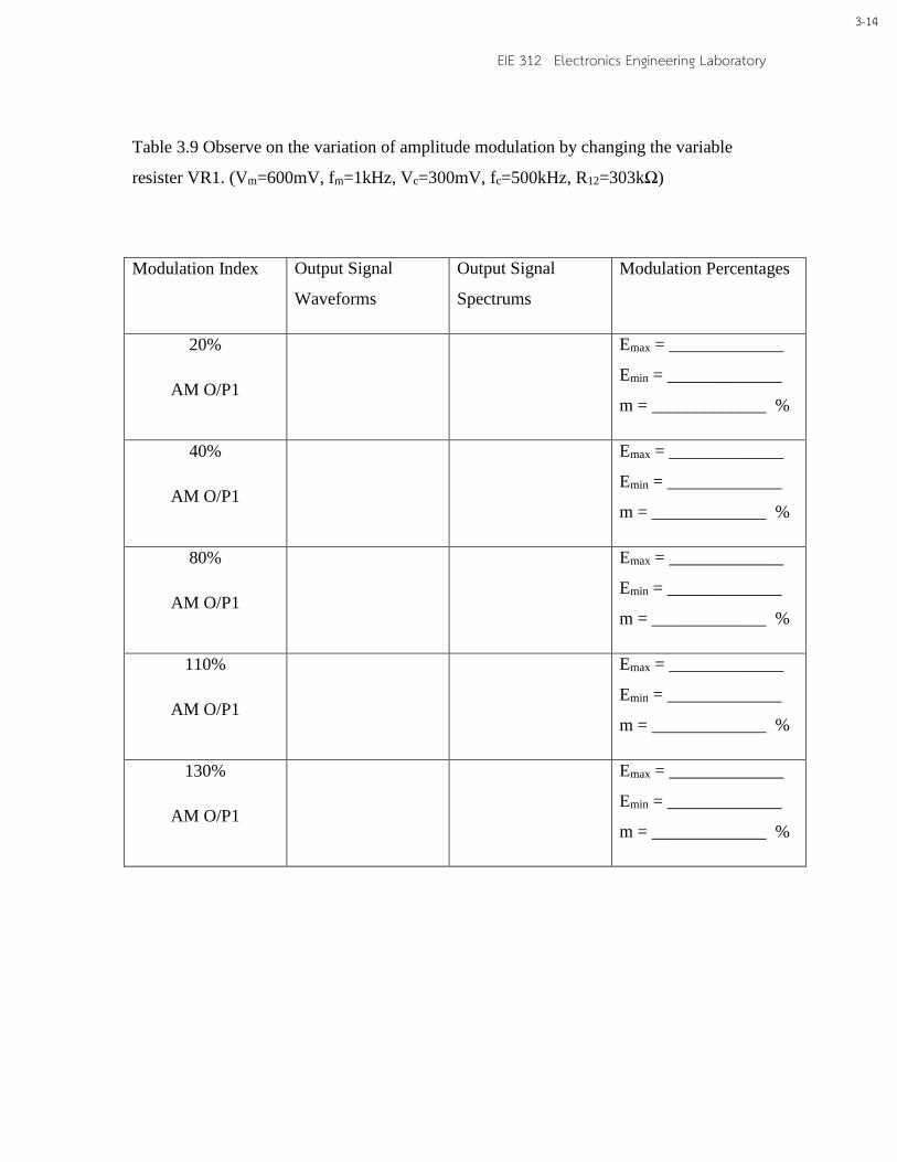
Table 3.9 Observe on the variation of amplitude modulation by changing the variable
resister VR1. (Vm=600mV, fm=1kHz, Vc=300mV, fc=500kHz, R12=303kΩ)
Modulation Index Output Signal
Waveforms
Output Signal
Spectrums
Modulation Percentages
20%
AM O/P1
Emax = _____________
Emin = _____________
m = _____________ %
40%
AM O/P1
Emax = _____________
Emin = _____________
m = _____________ %
80%
AM O/P1
Emax = _____________
Emin = _____________
m = _____________ %
110%
AM O/P1
Emax = _____________
Emin = _____________
m = _____________ %
130%
AM O/P1
Emax = _____________
Emin = _____________
m = _____________ %
EIE 312 Electronics Engineering Laboratory
3-15
3.5 : Problems Discussion
1. Explain the objectives of the transistor Q1 in figure 3.5.
2. Explain the objectives of the inductor L1, capacitor C3 and resistor R3 in figure 3-
5.
3. Explain the objectives of the variable resistor VR1 in figure 3-7.
4. Refer to figure 3-7, if we let J2 be short circuit, J1 be opened circuit, i.e. R10
changes to R12, which its value is 6.8kΩ changed to 3.3 kΩ. Then describe the
variation of the DC bias current of MC1496.
5. Refer to figure 3-7, if we adjust the magnitude of the variable resistor VR2 from
small to large, then describe the variation of the output signal of AM modulator.
6. When modulation index, m=80% and 130%, what are the ratio of Emax and Emin ?