Embed Size (px)
Citation preview
Experiment No: 1 Diode Characteristics
Objective: To study and verify the functionality of a) PN junction diode in forward bias
b) Point-Contact diode in reverse bias
Components/ Equipments Required:
Components Equipments
Sl.No. Name Quantity Name Quantity
1 Diode
(BY127, OA79)
1(One) No
each
DC Regulated Power supply
(0 - 30 V variable)
1(One) No.
2 Resistor
(1K )
1(One) No. Digital Ammeters
( 0 - 200 mA, 0 - 200 µA)
1(One) No.
Each
3 Bread board 1(One) No. Digital Voltmeter
(0 - 20V)
1(One) No.
4 Connecting wires (Single strand, Multi strand)
Biasing of PN junction Diode:
Forward bias operation
The P-N junction supports uni-directional current flow. If +ve terminal of the input supply is connected to P-
side and –ve terminal is connected the n side, then diode is said to be forward biased condition. In this condition
the height of the potential barrier at the junction is lowered by an amount equal to given forward biasing
voltage. Both the holes from p-side and electrons from n-side cross the junction simultaneously thereby
decreasing the depleted region. This constitutes a forward current (majority carrier movement – diffusion
current). Assuming current flowing through the diode to be very large, the diode can be approximated as short-
circuited switch. Diode offers a very small resistance called forward resistance (few ohms)
Reverse bias operation
If negative terminal of the input supply is connected to p-side and –ve terminal is connected to n-side then the
diode is said to be reverse biased. In this condition an amount equal to reverse biasing voltage increases the
height of the potential barrier at the junction. Both the holes on P-side and electrons on N-side tend to move
away from the junction there by increasing the depleted region. However the process cannot continue
indefinitely, thus a small current called reverse saturation current continues to flow in the diode. This current is
negligible; the diode can be approximated as an open circuited switch it offers a very high resistance called
reverse resistance(few Kiloohms).
Static Resistance: The opposition offered by a diode to the direct current flowing forward bias condition is known
as its DC forward resistance or Static Resistance. It is measured by taking the ratio of DC voltage across the diode
to the DC current flowing through it at an operating point.
Dynamic Resistance: The opposition offered by a diode to the changing current flow I forward bias condition
is known as its AC Forward Resistance. It is measured by a ratio of change in voltage across the diode to the
resulting change in current through it for an operating point P.
Average Resistance: Same as dynamic resistance but measured between extremities.
Diode current equation
The volt-ampere characteristics of a diode explained by the following equations:
Where I = current flowing in the diode,
I0 = reverse saturation current
V = voltage applied to the diode,
VT = volt- equivalent of temperature = k T/q = T/ 11,600 = 26mV (@ room temp)
=1 (for Ge) and 2 (for Si)
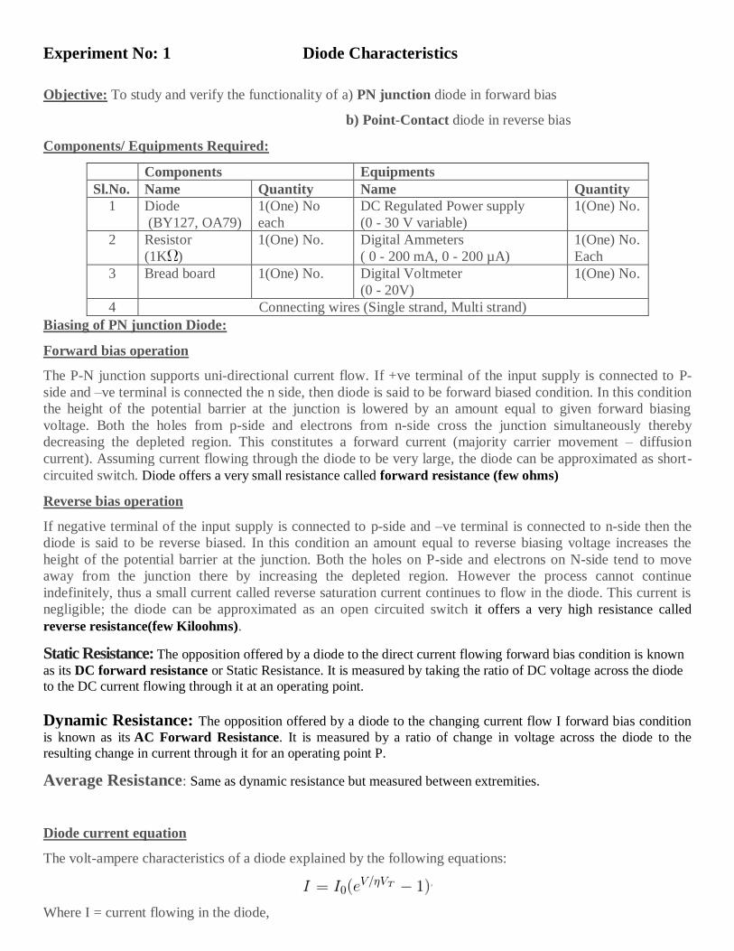
Circuit Diagram:
Fig. 1: Forward Bias Condition Fig. 2: Reverse Bias Condition
Procedure: (a) Forward Bias Condition:
1. Connect the circuit as shown in Fig.1 (PN Junction diode with milli-ammeter in series with the diode).
2. Initially vary Regulated Power Supply (RPS) voltage Vs in steps of 0.1 V. Once the current starts
increasing vary Vs in steps of 0.02V and note down the corresponding readings Vf and If.
3. Tabulate different forward currents obtained for different forward voltages.
4. Plot the V-I characteristics and calculate the resistance levels
5. Compare the theoretical and practical values (cut-in voltage and resistances).
Tabular column:
Forward bias Reverse bias
VD(volts) ID ( mA) VD(volts) ID ( µA)
(b) Reverse Bias Condition:
1. Connect the circuit as shown in Fig.2 (Point contact diode in series with micro ammeter).
2. Vary Vs in the Regulated Power Supply (RPS) gradually in steps of 1V from 0V to 12V and note down
the corresponding readings Vr and Ir.
3. Tabulate different reverse currents obtained for different reverse voltages.
4. Plot the V-I characteristics and calculate the resistance levels
5. Compare the theoretical and practical values.
Ideal characteristics
Forward Characteristic Reverse Characteristic
Calculations from Graph:
a) Forward Bias of PN Junction Diode:
Cut-in Voltage V =
Static forward Resistance
Dynamic Forward Resistance
Average Resistance ravg = / pt to pt
b) Reverse Bias of Point contact diode:
Similarly find static and dynamic resistances
Result: Volt-Ampere Characteristics of P-N Diode are studied.
Application of Diode;
Outcomes: Students are able to
1. Analyze the characteristics of PN diode.
2. Calculate the resistance in forward bias and reverse bias.
Experiment No: 2 Common Emitter Configuration Characteristics
Objective: To study the input and output characteristics of a transistor (Common Emitter configuration).
Component/ Equipment required:
Component Equipment
Sl. No. Name Quantity Name Quantity
1 Transistor-npn
BC 107
1(One) No. DC Regulated Power supply
(0 - 30 V)
2 (One)
No.
2 Resistors
(1K , 100K )
1(One) No.
Each
Digital Ammeters
(0 - 200 mA, 0-200 A)
1(One) No.
Each
3 Bread board 1(One) No. Digital Voltmeter
(0 - 20V)
2(Two) No.
4 Connecting wires (Single Strand)
Specifications: For Transistor BC 107: Max Collector Current = 0.1A; VCEO max = 50V
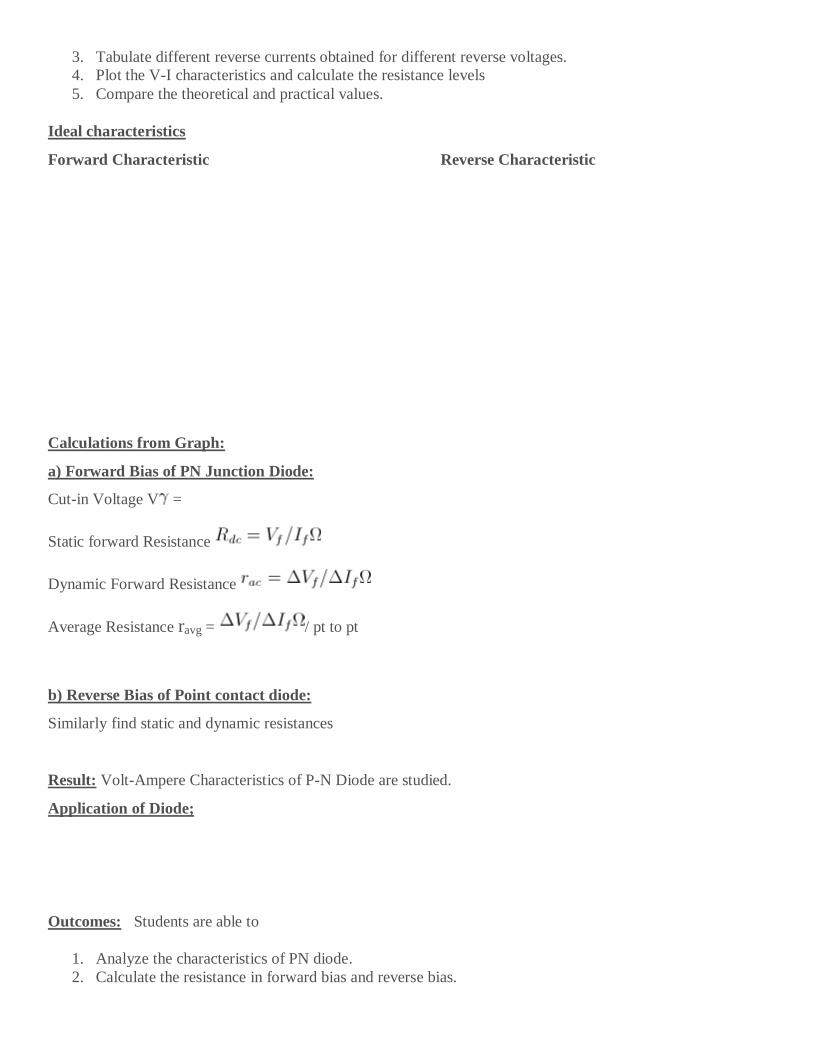
Circuit Diagram:
Fig. 1: Common emitter circuit. Pin assignment of Transistor:
View from side of pins View from top of casing
Operation:
The input is applied between base and emitter, the output is taken between collector and emitter. Input
characteristics are obtained between the input current IB and input voltage VBE at constant output voltage VCE.
This portion of an NPN BJT is just like a p-n junction. Consequently, the IB and VBE relationship in the
common emitter configuration is the same as the I-V characteristic of a diode. The typical value of VBE for a
silicon BJT is 0.7 V.
Output characteristics are obtained between the output voltage VCE and output current IC at constant input
current IB. The output I-V characteristic consists of a set of curves, one for each value of IB. In the common
emitter configuration, all the I-V curves start from IC = 0 and VCE and equal to some threshold value. For a
given value of IB, the curve increases steeply until it reaches a level proportional to IB, at which point it flattens
(but not completely).
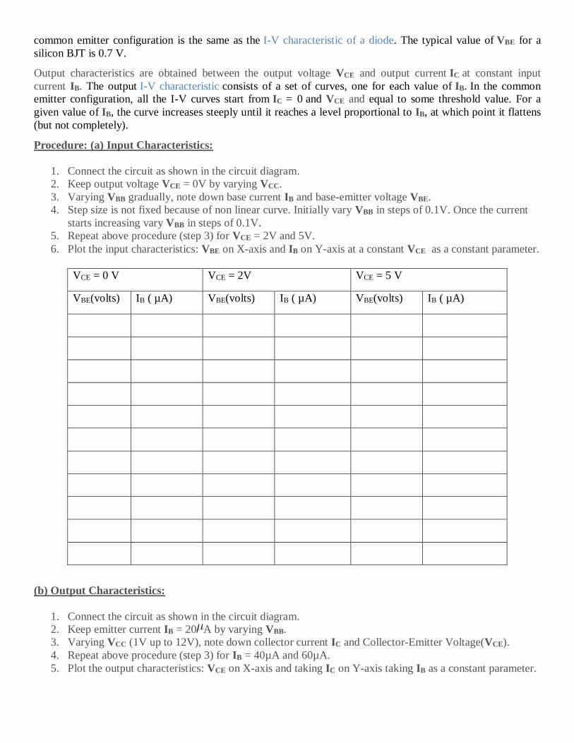
Procedure: (a) Input Characteristics:
1. Connect the circuit as shown in the circuit diagram.
2. Keep output voltage VCE = 0V by varying VCC.
3. Varying VBB gradually, note down base current IB and base-emitter voltage VBE.
4. Step size is not fixed because of non linear curve. Initially vary VBB in steps of 0.1V. Once the current
starts increasing vary VBB in steps of 0.1V.
5. Repeat above procedure (step 3) for VCE = 2V and 5V.
6. Plot the input characteristics: VBE on X-axis and IB on Y-axis at a constant VCE as a constant parameter.
VCE = 0 V VCE = 2V VCE = 5 V
VBE(volts) IB ( µA) VBE(volts) IB ( µA) VBE(volts) IB ( µA)
(b) Output Characteristics:
1. Connect the circuit as shown in the circuit diagram.
2. Keep emitter current IB = 20 A by varying VBB.
3. Varying VCC (1V up to 12V), note down collector current IC and Collector-Emitter Voltage(VCE).
4. Repeat above procedure (step 3) for IB = 40µA and 60µA.
5. Plot the output characteristics: VCE on X-axis and taking IC on Y-axis taking IB as a constant parameter.
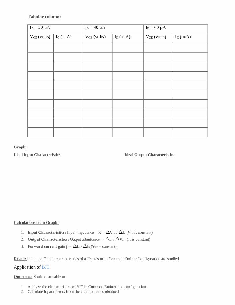
Tabular column:
IB = 20 µA IB = 40 µA IB = 60 µA
VCE (volts) IC ( mA) VCE (volts) IC ( mA) VCE (volts) IC ( mA)
Graph:
Ideal Input Characteristics Ideal Output Characteristics
Calculations from Graph:
1. Input Characteristics: Input impedance = Ri = VBE / IB (VCE is constant)
2. Output Characteristics: Output admittance = IC / VCE (IB is constant)
3. Forward current gain β = IC / IB (VCE = constant)
Result: Input and Output characteristics of a Transistor in Common Emitter Configuration are studied.
Application of BJT:
Outcomes: Students are able to
1. Analyze the characteristics of BJT in Common Emitter and configuration.
2. Calculate h-parameters from the characteristics obtained.
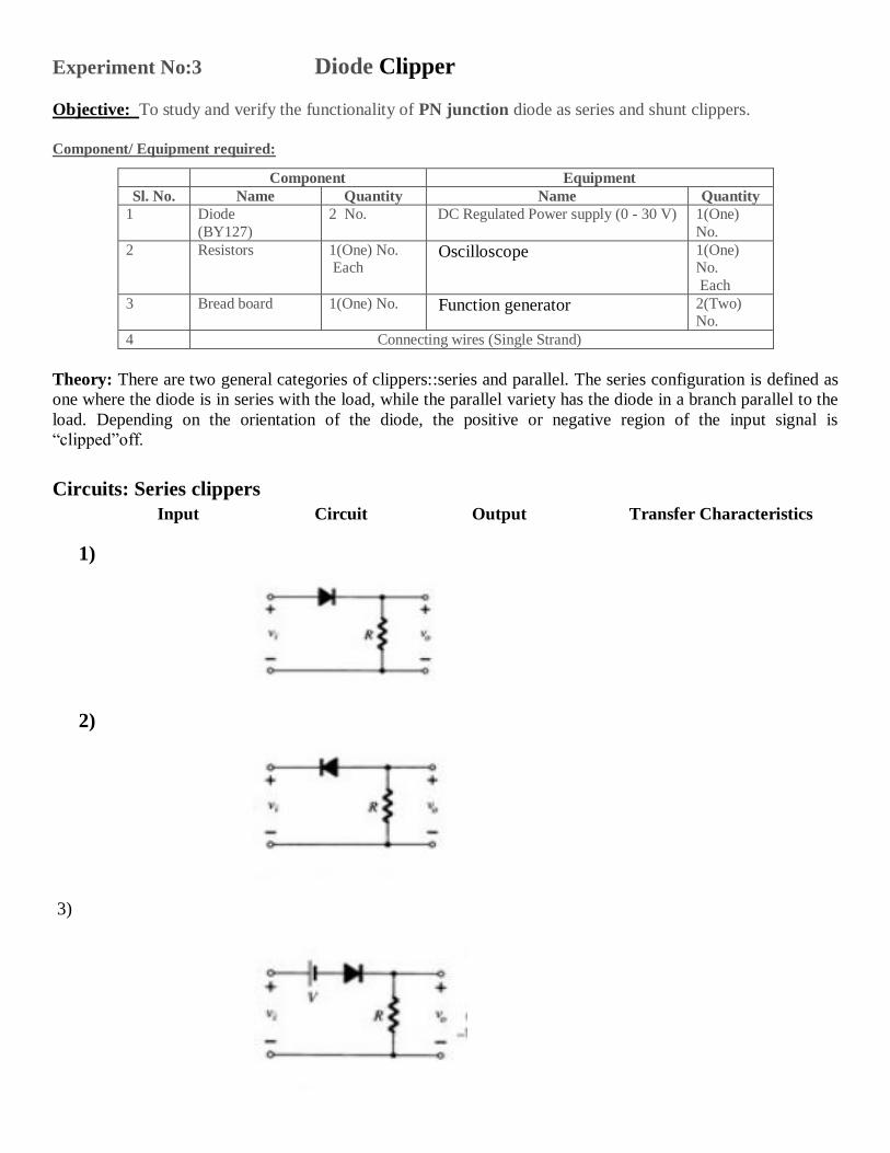
Experiment No:3 Diode Clipper
Objective: To study and verify the functionality of PN junction diode as series and shunt clippers.
Component/ Equipment required:
Component Equipment
Sl. No. Name Quantity Name Quantity
1 Diode
(BY127)
2 No. DC Regulated Power supply (0 - 30 V) 1(One)
No.
2 Resistors 1(One) No.
Each Oscilloscope
1(One)
No.
Each
3 Bread board 1(One) No. Function generator 2(Two)
No.
4 Connecting wires (Single Strand)
Theory: There are two general categories of clippers::series and parallel. The series configuration is defined as
one where the diode is in series with the load, while the parallel variety has the diode in a branch parallel to the
load. Depending on the orientation of the diode, the positive or negative region of the input signal is
“clipped”off.
Circuits: Series clippers
Input Circuit Output Transfer Characteristics
1)
2)
3)
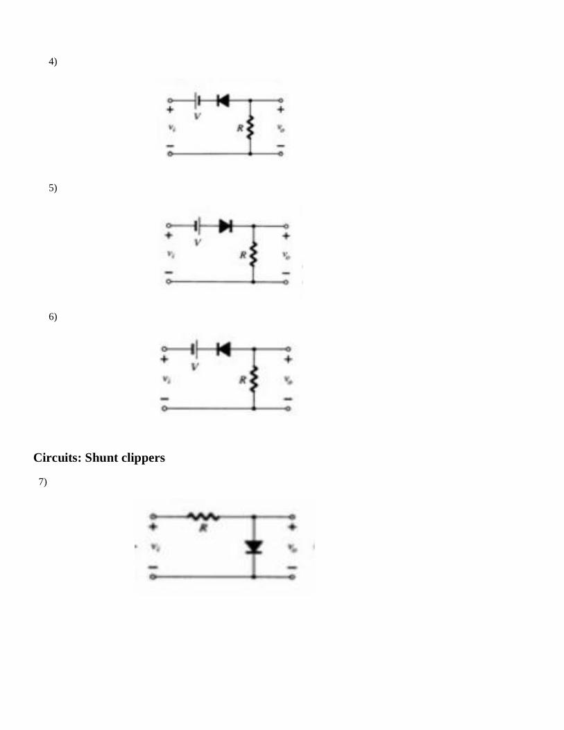
4)
5)
6)
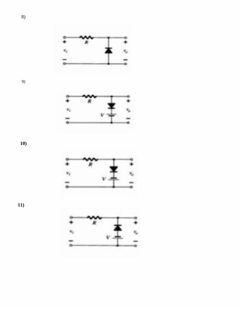
Circuits: Shunt clippers
7)
8)
9)
10)
11)
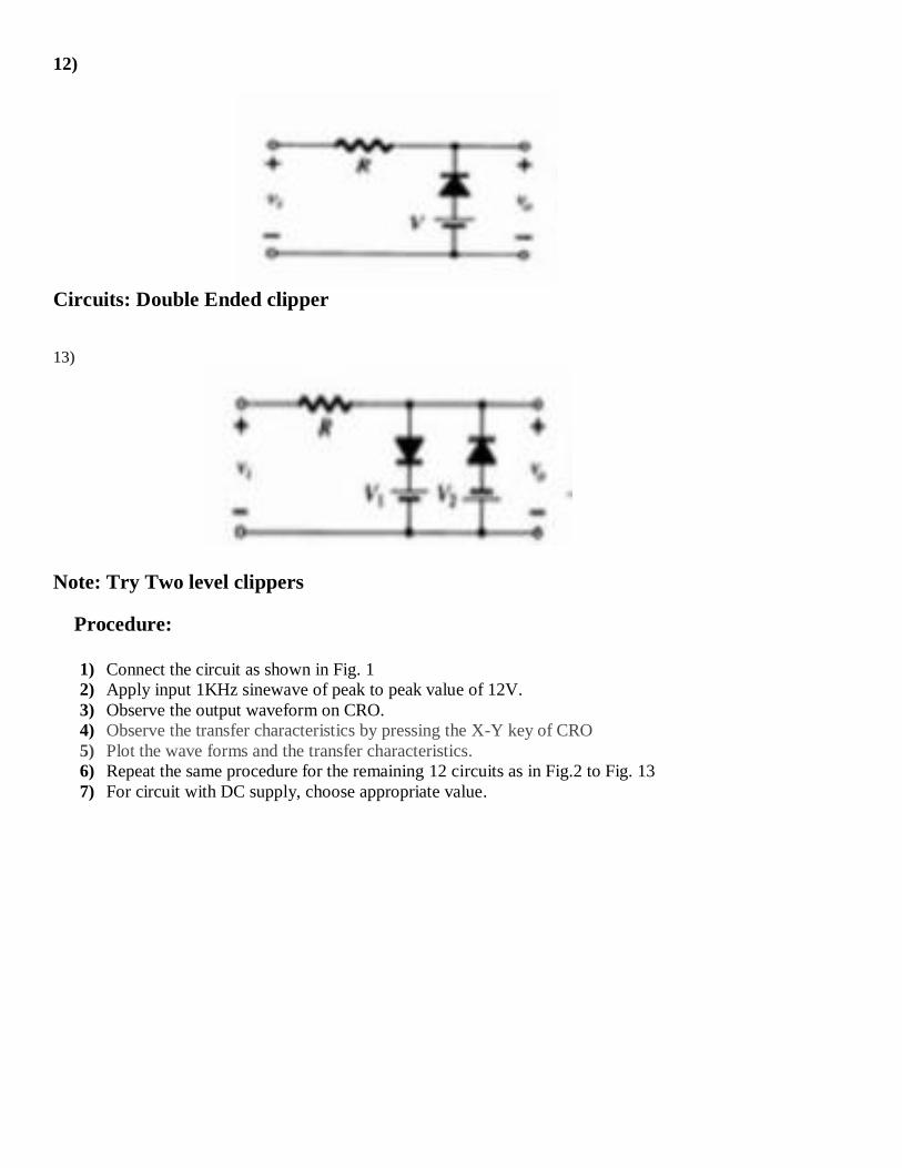
12)
Circuits: Double Ended clipper
13)
Note: Try Two level clippers
Procedure:
1) Connect the circuit as shown in Fig. 1
2) Apply input 1KHz sinewave of peak to peak value of 12V.
3) Observe the output waveform on CRO.
4) Observe the transfer characteristics by pressing the X-Y key of CRO
5) Plot the wave forms and the transfer characteristics.
6) Repeat the same procedure for the remaining 12 circuits as in Fig.2 to Fig. 13
7) For circuit with DC supply, choose appropriate value.
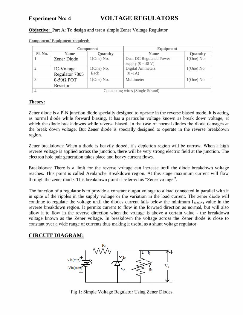
Experiment No: 4 VOLTAGE REGULATORS
Objective: Part A: To design and test a simple Zener Voltage Regulator
Component/ Equipment required:
Component Equipment
Sl. No. Name Quantity Name Quantity
1 Zener Diode 1(One) No. Dual DC Regulated Power
supply (0 - 30 V)
1(One) No.
2 IC-Voltage
Regulator 7805
1(One) No.
Each
Digital Ammeters
(0 -1A)
1(One) No.
3 0-50Ω POT
Resistor
1(One) No. Multimeter 1(One) No.
4 Connecting wires (Single Strand)
Theory:
Zener diode is a P-N junction diode specially designed to operate in the reverse biased mode. It is acting
as normal diode while forward biasing. It has a particular voltage known as break down voltage, at
which the diode break downs while reverse biased. In the case of normal diodes the diode damages at
the break down voltage. But Zener diode is specially designed to operate in the reverse breakdown
region.
Zener breakdown: When a diode is heavily doped, it’s depletion region will be narrow. When a high
reverse voltage is applied across the junction, there will be very strong electric field at the junction. The
electron hole pair generation takes place and heavy current flows.
Breakdown: There is a limit for the reverse voltage can increase until the diode breakdown voltage
reaches. This point is called Avalanche Breakdown region. At this stage maximum current will flow
through the zener diode. This breakdown point is referred as “Zener voltage”.
The function of a regulator is to provide a constant output voltage to a load connected in parallel with it
in spite of the ripples in the supply voltage or the variation in the load current. The zener diode will
continue to regulate the voltage until the diodes current falls below the minimum IZ(MIN) value in the
reverse breakdown region. It permits current to flow in the forward direction as normal, but will also
allow it to flow in the reverse direction when the voltage is above a certain value - the breakdown
voltage known as the Zener voltage. In breakdown the voltage across the Zener diode is close to
constant over a wide range of currents thus making it useful as a shunt voltage regulator.
CIRCUIT DIAGRAM:
Fig 1: Simple Voltage Regulator Using Zener Diodes
Design:
A typical Zener diode shunt regulator is shown in Fig.1. The resistor is selected so that when the input
voltage is at VIN(min) and the load current is at IL(max) that the current through the Zener diode is at least
IZ(min). A Zener diode of break down voltage VZ is reverse connected to an input voltage source Vi across
a load resistance RL and a series resistor RS. The voltage across the Zener will remain steady at its break
down voltage VZ for all the values of Zener current IZ as long as the current remains in the break down
region. Hence a regulated DC output voltage V0 = VZ is obtained across RL .
With the input voltage is at Vin (min) & Load Current at IL(MAX) , current through the series resistance RS
I=I max + IZ (min)
The voltage across Rs, VRS = V IN (max) – V Z
Therefore RS = VRS / I = V IN (min) – VZ / IL max + I Z min
Select the nearest standard value for RS
The Maximum input voltage at which the regulator is effective is given by
VIN(max) = V IN(min) + I RS
Thus, the regulation is effective only between VIN (min) and V In (max)
Design the Zener Voltage Regulator for the following specifications:
V in (min)= 12v Vo= 5.6v IL = 5mA to 30mA (Variable)
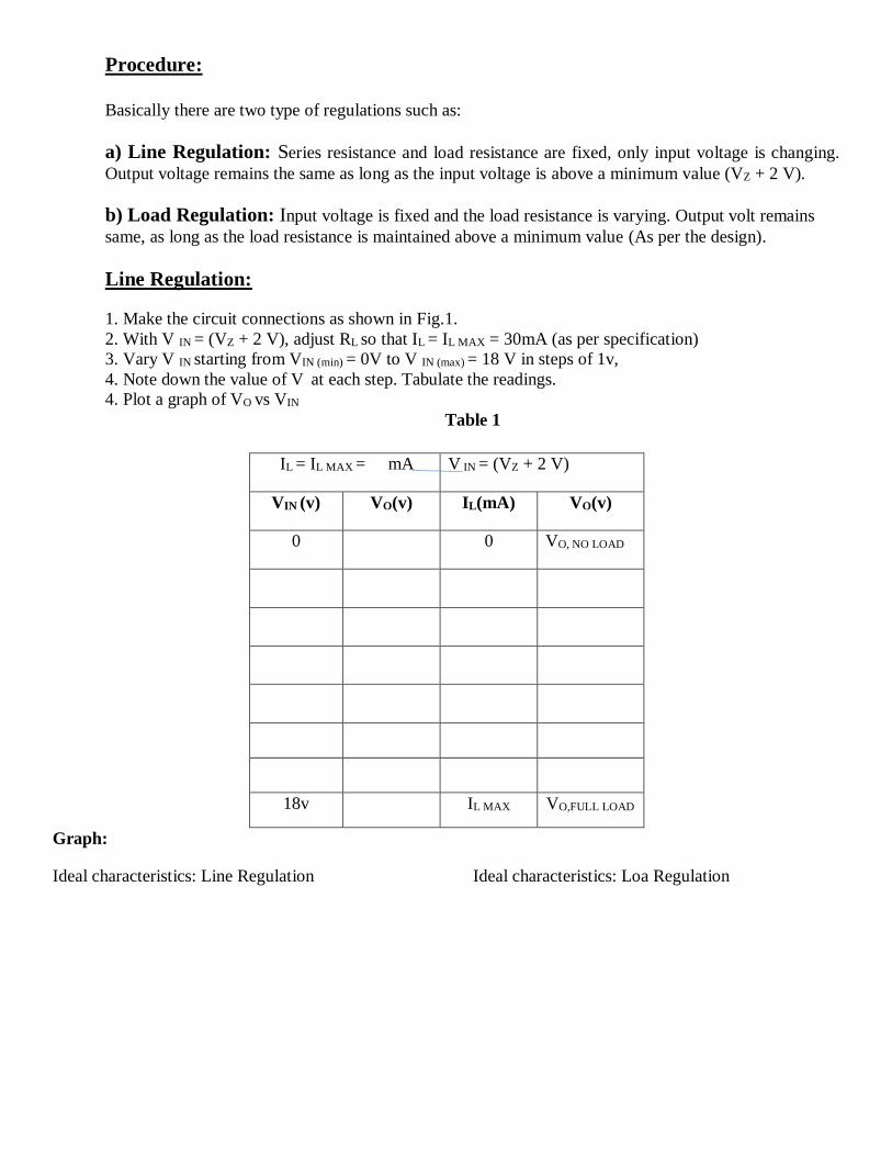
Procedure:
Basically there are two type of regulations such as:
a) Line Regulation: Series resistance and load resistance are fixed, only input voltage is changing.
Output voltage remains the same as long as the input voltage is above a minimum value (VZ + 2 V).
b) Load Regulation: Input voltage is fixed and the load resistance is varying. Output volt remains
same, as long as the load resistance is maintained above a minimum value (As per the design).
Line Regulation:
1. Make the circuit connections as shown in Fig.1.
2. With V IN = (VZ + 2 V), adjust RL so that IL = IL MAX = 30mA (as per specification)
3. Vary V IN starting from VIN (min) = 0V to V IN (max) = 18 V in steps of 1v,
4. Note down the value of V at each step. Tabulate the readings.
4. Plot a graph of VO vs VIN
Table 1
IL = IL MAX = mA V IN = (VZ + 2 V)
VIN (v) VO(v) IL(mA) VO(v)
0 0 VO, NO LOAD
18v IL MAX VO,FULL LOAD
Graph:
Ideal characteristics: Line Regulation Ideal characteristics: Loa Regulation
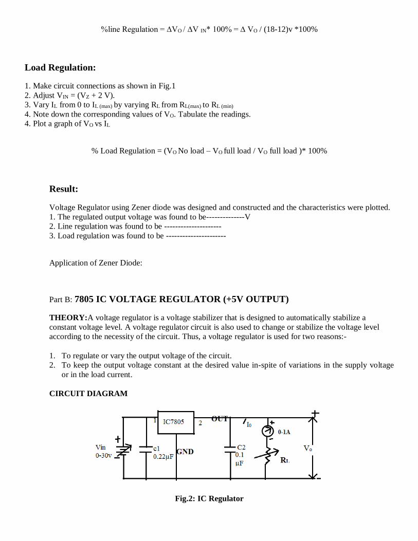
%line Regulation = ∆VO / ∆V IN* 100% = ∆ VO / (18-12)v *100%
Load Regulation:
1. Make circuit connections as shown in Fig.1
2. Adjust VIN = (VZ + 2 V).
3. Vary IL from 0 to IL (max) by varying RL from RL(max) to RL (min)
4. Note down the corresponding values of VO. Tabulate the readings.
4. Plot a graph of VO vs IL
% Load Regulation = (VO No load – VO full load / VO full load )* 100%
Result:
Voltage Regulator using Zener diode was designed and constructed and the characteristics were plotted.
1. The regulated output voltage was found to be--------------V
2. Line regulation was found to be ---------------------
3. Load regulation was found to be ----------------------
Application of Zener Diode:
Part B: 7805 IC VOLTAGE REGULATOR (+5V OUTPUT)
THEORY:A voltage regulator is a voltage stabilizer that is designed to automatically stabilize a
constant voltage level. A voltage regulator circuit is also used to change or stabilize the voltage level
according to the necessity of the circuit. Thus, a voltage regulator is used for two reasons:-
1. To regulate or vary the output voltage of the circuit.
2. To keep the output voltage constant at the desired value in-spite of variations in the supply voltage
or in the load current.
CIRCUIT DIAGRAM
Fig.2: IC Regulator
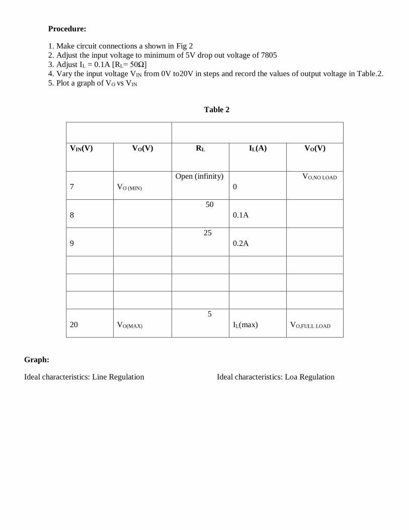
Procedure:
1. Make circuit connections a shown in Fig 2
2. Adjust the input voltage to minimum of 5V drop out voltage of 7805
3. Adjust IL = 0.1A [RL= 50Ω]
4. Vary the input voltage VIN from 0V to20V in steps and record the values of output voltage in Table.2.
5. Plot a graph of VO vs VIN
Table 2
VIN(V) VO(V) RL IL(A) VO(V)
7
VO (MIN)
Open (infinity)
0
VO,NO LOAD
8
50
0.1A
9
25
0.2A
20
VO(MAX)
5
IL(max)
VO,FULL LOAD
Graph:
Ideal characteristics: Line Regulation Ideal characteristics: Loa Regulation
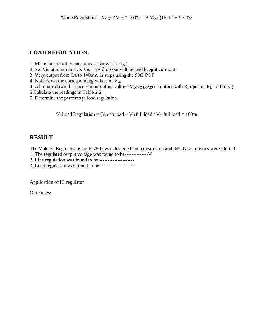
%line Regulation = ∆VO/ ∆V IN * 100% = ∆ VO / (18-12)v *100%
LOAD REGULATION:
1. Make the circuit connections as shown in Fig.2
2. Set VIN at minimum i.e, VIN= 5V drop out voltage and keep it constant
3. Vary output from 0A to 100mA in steps using the 50Ω POT
4. Note down the corresponding values of VO.
4. Also note down the open-circuit output voltage VO, NO LOAD(i.e output with RL open or RL =infinity )
5.Tabulate the readings in Table 2.2
5. Determine the percentage load regulation.
% Load Regulation = (VO no load – VO full load / VO full load)* 100%
RESULT:
The Voltage Regulator using IC7805 was designed and constructed and the characteristics were plotted.
1. The regulated output voltage was found to be--------------V
2. Line regulation was found to be ---------------------
3. Load regulation was found to be ----------------------
Application of IC regulator
Outcomes:
Experiment No: 5 OPERATIONAL AMPLIFIER CIRCUITS - 1
Objective: To design and test Op-Amp as an amplifier and an arithmetic operator
Theory: An operational amplifier (Op-amp) is an integrated circuit (IC) that operates as a
voltage amplifier. These amplifiers are called "operation" amplifiers because they were initially
designed as an effective device for performing arithmetic operations (like addition, subtraction, and
etc.,) in an analog circuit. An op-amp has a differential input (two inputs of opposite polarity). An op-
amp has a single output and a very high gain.
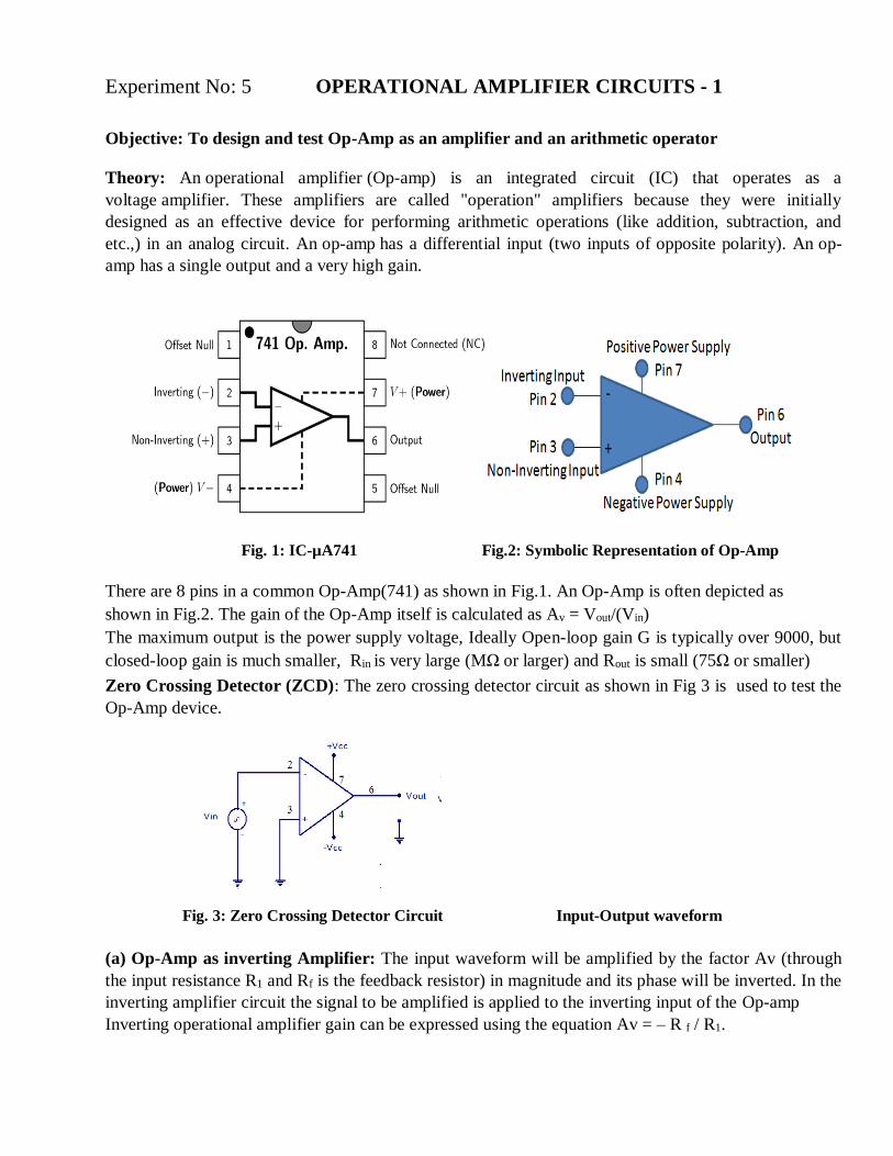
Fig. 1: IC-µA741 Fig.2: Symbolic Representation of Op-Amp
There are 8 pins in a common Op-Amp(741) as shown in Fig.1. An Op-Amp is often depicted as
shown in Fig.2. The gain of the Op-Amp itself is calculated as Av = Vout/(Vin)
The maximum output is the power supply voltage, Ideally Open-loop gain G is typically over 9000, but
closed-loop gain is much smaller, Rin is very large (MΩ or larger) and Rout is small (75Ω or smaller)
Zero Crossing Detector (ZCD): The zero crossing detector circuit as shown in Fig 3 is used to test the
Op-Amp device.
Fig. 3: Zero Crossing Detector Circuit Input-Output waveform
(a) Op-Amp as inverting Amplifier: The input waveform will be amplified by the factor Av (through
the input resistance R1 and Rf is the feedback resistor) in magnitude and its phase will be inverted. In the
inverting amplifier circuit the signal to be amplified is applied to the inverting input of the Op-amp
Inverting operational amplifier gain can be expressed using the equation Av = – R f / R1.
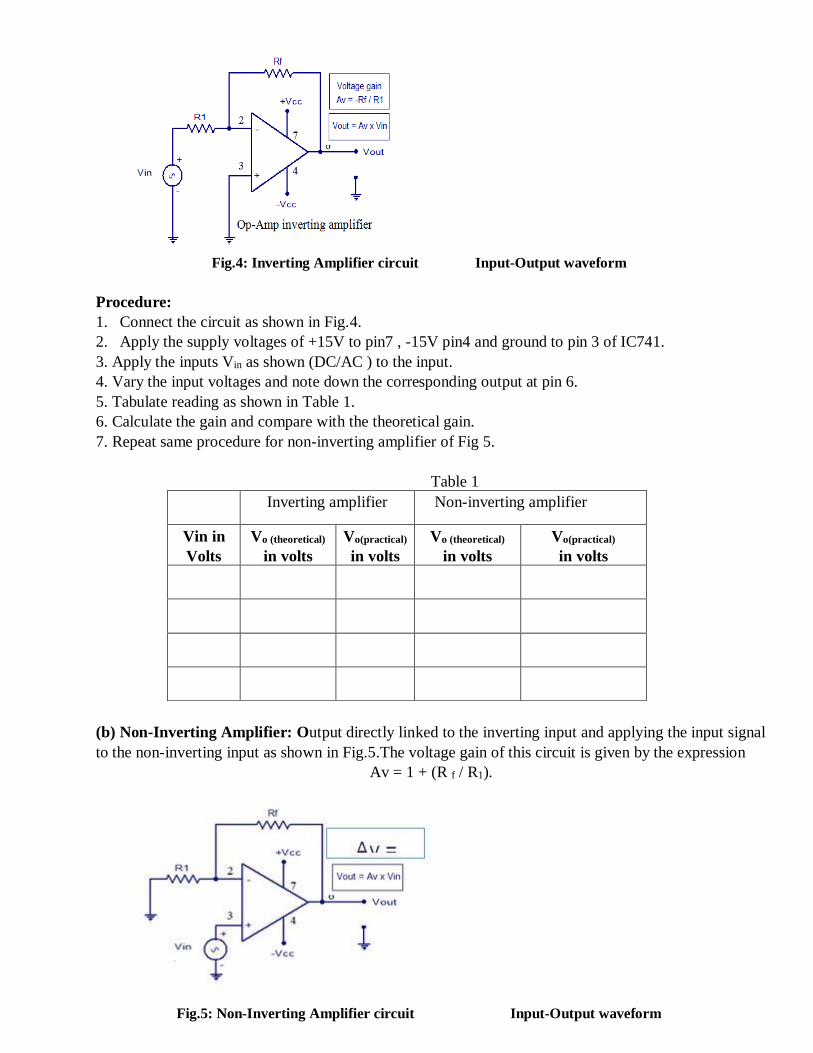
Fig.4: Inverting Amplifier circuit Input-Output waveform
Procedure:
1. Connect the circuit as shown in Fig.4.
2. Apply the supply voltages of +15V to pin7 , -15V pin4 and ground to pin 3 of IC741.
3. Apply the inputs Vin as shown (DC/AC ) to the input.
4. Vary the input voltages and note down the corresponding output at pin 6.
5. Tabulate reading as shown in Table 1.
6. Calculate the gain and compare with the theoretical gain.
7. Repeat same procedure for non-inverting amplifier of Fig 5.
Table 1
(b) Non-Inverting Amplifier: Output directly linked to the inverting input and applying the input signal
to the non-inverting input as shown in Fig.5.The voltage gain of this circuit is given by the expression
Av = 1 + (R f / R1).
Fig.5: Non-Inverting Amplifier circuit Input-Output waveform
Inverting amplifier Non-inverting amplifier
Vin in
Volts
Vo (theoretical)
in volts
Vo(practical)
in volts
Vo (theoretical)
in volts
Vo(practical)
in volts
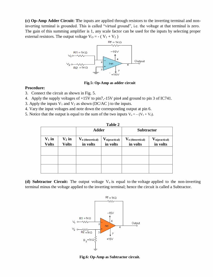
(c) Op-Amp Adder Circuit: The inputs are applied through resistors to the inverting terminal and non-
inverting terminal is grounded. This is called “virtual ground”, i.e. the voltage at that terminal is zero.
The gain of this summing amplifier is 1, any scale factor can be used for the inputs by selecting proper
external resistors. The output voltage VO = - ( V1 + V2 )
Fig.5: Op-Amp as adder circuit
Procedure:
3. Connect the circuit as shown in Fig. 5.
4. Apply the supply voltages of +15V to pin7,-15V pin4 and ground to pin 3 of IC741.
3. Apply the inputs V1 and V2 as shown (DC/AC ) to the inputs.
4. Vary the input voltages and note down the corresponding output at pin 6.
5. Notice that the output is equal to the sum of the two inputs Vo = – (V1 + V2).
Table 2
Adder Subtractor
V1 in
Volts
V2 in
Volts
Vo (theoretical)
in volts
Vo(practical)
in volts
Vo (theoretical)
in volts
Vo(practical)
in volts
(d) Subtractor Circuit: The output voltage Vo is equal to the voltage applied to the non-inverting
terminal minus the voltage applied to the inverting terminal; hence the circuit is called a Subtractor.
Fig.6: Op-Amp as Subtractor circuit.
Procedure:
1. Connect the circuit as shown in Fig.6.
2. Apply the supply voltages of +15V to pin7,-15V pin4 and ground to pin 3 of IC741.
3. Apply the inputs V1 and V2. (DC/AC ) to the inputs.
4. Vary the input voltages and note down the corresponding output at pin 6 of the IC 741
5. Notice that the output is equal to the difference of the two inputs Vo = V2 – V1.
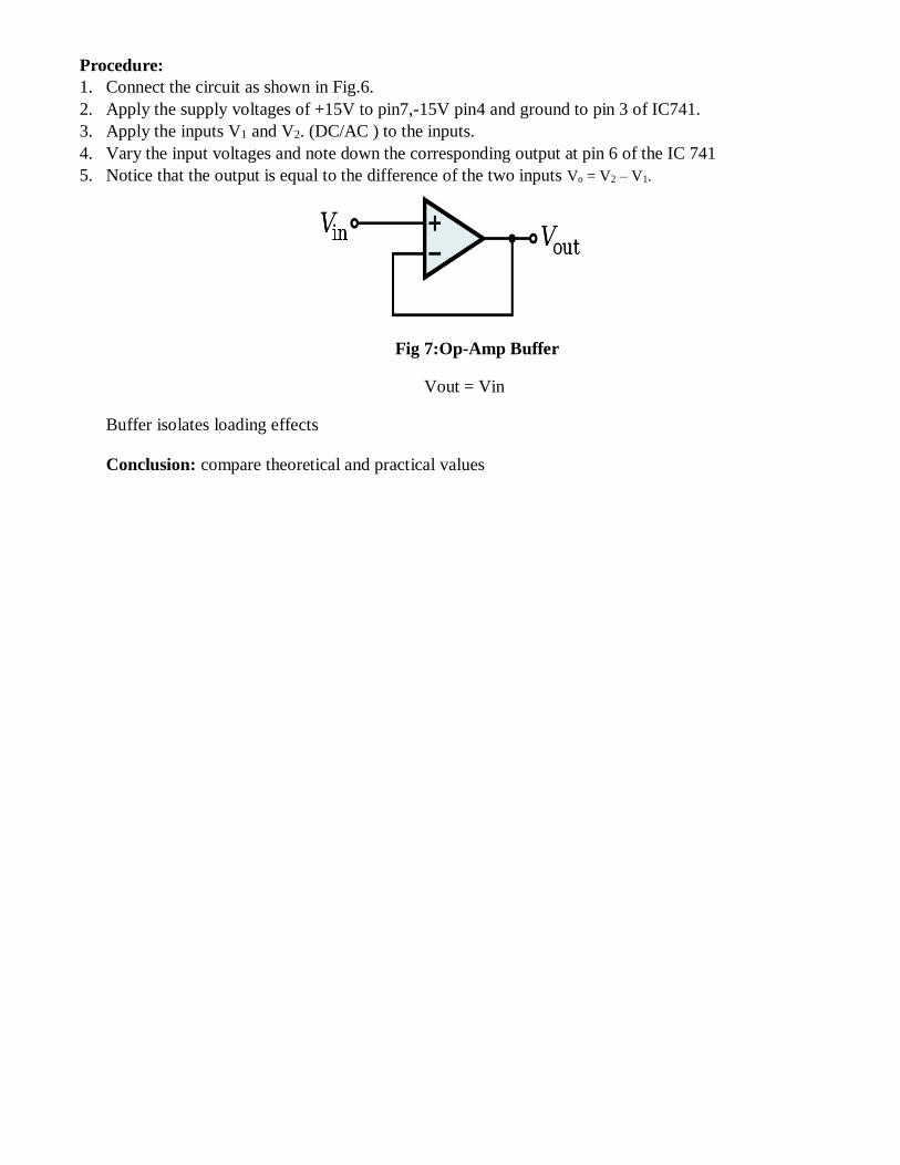
Fig 7:Op-Amp Buffer
Vout = Vin
Buffer isolates loading effects
Conclusion: compare theoretical and practical values