Embed Size (px)
Citation preview
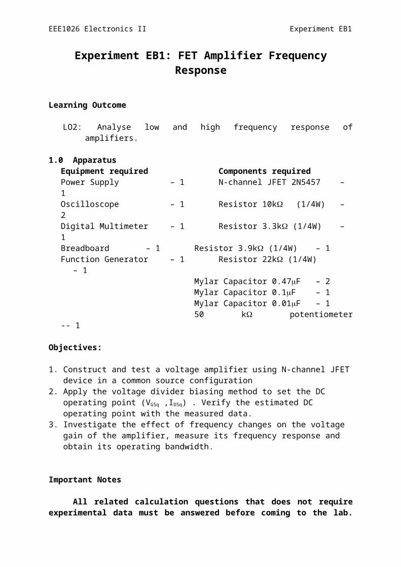
EEE1026 Electronics II Experiment EB1
Experiment EB1: FET Amplifier Frequency Response
Learning Outcome
LO2: Analyse low and high frequency response of amplifiers.
1.0 ApparatusEquipment required Components requiredPower Supply – 1 N-channel JFET 2N5457 – 1Oscilloscope – 1 Resistor 10k (1/4W) – 2Digital Multimeter – 1 Resistor 3.3k (1/4W) – 1Breadboard – 1 Resistor 3.9k (1/4W) – 1Function Generator – 1 Resistor 22k (1/4W) – 1
Mylar Capacitor 0.47F – 2Mylar Capacitor 0.1F – 1Mylar Capacitor 0.01F – 150 k potentiometer -- 1
Objectives:
1. Construct and test a voltage amplifier using N-channel JFET device in a common source configuration
2. Apply the voltage divider biasing method to set the DC operating point (VGSq ,IDSq) . Verify the estimated DC operating point with the measured data.
3. Investigate the effect of frequency changes on the voltage gain of the amplifier, measure its frequency response and obtain its operating bandwidth.
Important Notes
All related calculation questions that does not require experimental data must be answered before coming to the lab. You are required to show all the calculation steps when requested by the lab instructor. During the evaluation session, your lab instructor may request you to demonstrate how the measurement data is obtained and explain your experimental results.
Report Submission
You must obtain the signature of the Instructor after completing each section of the experiment. Together with Rubric assessment form, Submit your report to the Lab Supervisor, immediately after the experiment.
EEE1026 Electronics II Experiment EB1
2.0 Background Theory
An amplifier is a circuit that increases/decrease the input signal value and in this experiment the signal to be amplified is the voltage. In this experiment you are going to investigate frequency response characteristic of a voltage amplifier circuit using the N-channel JFET device.
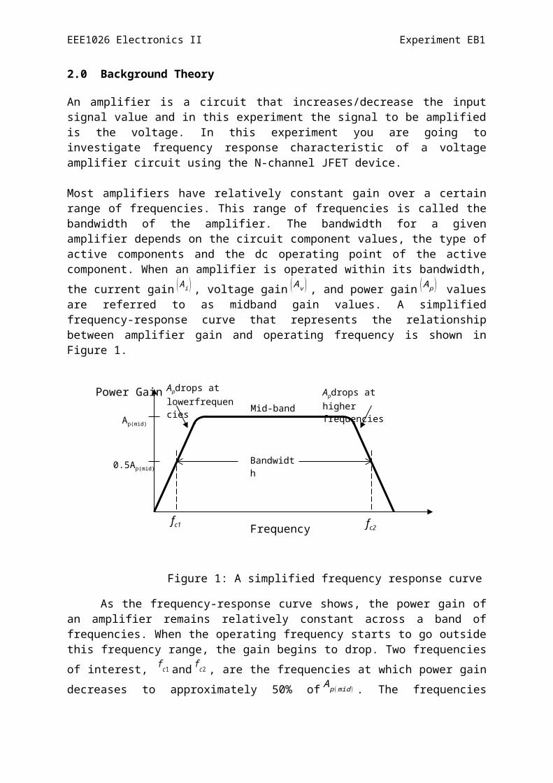
Most amplifiers have relatively constant gain over a certain range of frequencies. This range of frequencies is called the bandwidth of the amplifier. The bandwidth for a given amplifier depends on the circuit component values, the type of active components and the dc operating point of the active component. When an amplifier is operated within its bandwidth, the
current gain( A i ) , voltage gain( Av ) , and power gain( A p) values are referred to as midband gain values. A simplified frequency-response curve that represents the relationship between amplifier gain and operating frequency is shown in Figure 1.
Figure 1: A simplified frequency response curve
As the frequency-response curve shows, the power gain of an amplifier remains relatively constant across a band of frequencies. When the operating frequency starts to go
outside this frequency range, the gain begins to drop. Two frequencies of interest, f c1 andf c2
, are the frequencies at which power gain decreases to approximately 50% of Ap (mid ) . The
frequencies labeled f c1 and f c2 are called the lower and upper cutoff frequencies of an amplifier, respectively. These frequencies are considered to be the bandwidth limits for the amplifier and thus bandwidth BW is given by
BW= f c2− f c1 .
The geometric average of f c1 and f c2 is called the geometric center frequency fo of an amplifier, given by
f 0=√ f c 1 f c 2 .
When the operating frequency is equal tof 0 , the power gain of the amplifier is at its maximum value.
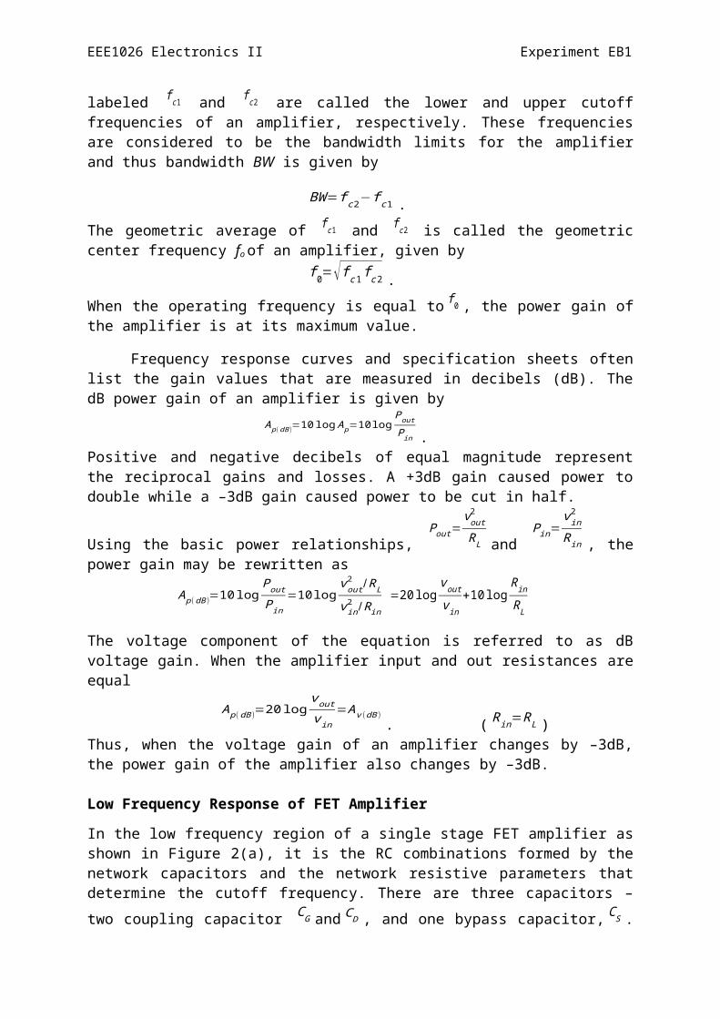
Frequency response curves and specification sheets often list the gain values that are measured in decibels (dB). The dB power gain of an amplifier is given by
Mid-band
Power Gai
Frequency
Ap(mid)
0.5Ap(mid)Bandwidth
fc2fc1
Apdrops at higher frequencies
Apdrops at lowerfrequencies
EEE1026 Electronics II Experiment EB1
Ap (dB )=10 log A p=10 logPout
Pin .Positive and negative decibels of equal magnitude represent the reciprocal gains and losses. A +3dB gain caused power to double while a –3dB gain caused power to be cut in half.
Using the basic power relationships, Pout=
vout2
RL and Pin=
v in2
R in , the power gain may be rewritten as
Ap (dB )=10 logPout
Pin=10 log
vout2 /RL
v in2 /R in
=20 logv out
vin+10 log
Rin
RL
The voltage component of the equation is referred to as dB voltage gain. When the amplifier input and out resistances are equal
Ap (dB )=20 logvout
v in=Av (dB )
. (Rin=RL )Thus, when the voltage gain of an amplifier changes by –3dB, the power gain of the amplifier also changes by –3dB.
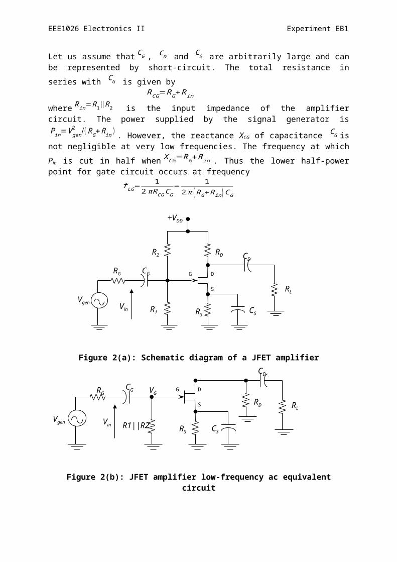
Low Frequency Response of FET Amplifier
In the low frequency region of a single stage FET amplifier as shown in Figure 2(a), it is the RC combinations formed by the network capacitors and the network resistive parameters that
determine the cutoff frequency. There are three capacitors – two coupling capacitor CG andCD , and one bypass capacitor,CS . Let us assume thatCG , CD and CS are arbitrarily large
and can be represented by short-circuit. The total resistance in series with CG is given byRCG=RG+Rin
whereRin=R1||R2 is the input impedance of the amplifier circuit. The power supplied by the
signal generator isPin=V gen2 /( RG+Rin ) . However, the reactance XCG of capacitance CG is not
negligible at very low frequencies. The frequency at which Pin is cut in half whenXCG=RG+Rin . Thus the lower half-power point for gate circuit occurs at frequency
f LG= 12 πRCG CG
= 12π (RG+R in)CG
Vin
G
S
D
Vgen
+VDD
RG CG
CS
CDRD
RL
R2
RSR1
EEE1026 Electronics II Experiment EB1
Figure 2(a): Schematic diagram of a JFET amplifier
Figure 2(b): JFET amplifier low-frequency ac equivalent circuit
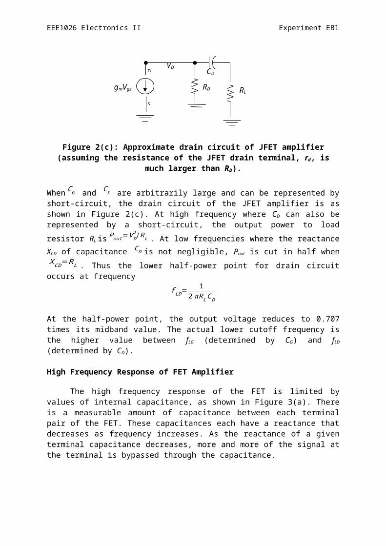
Figure 2(c): Approximate drain circuit of JFET amplifier (assuming the resistance of the JFET drain terminal, rd, is much larger than RD).
WhenCG and CS are arbitrarily large and can be represented by short-circuit, the drain circuit of the JFET amplifier is as shown in Figure 2(c). At high frequency where CD can also
be represented by a short-circuit, the output power to load resistor RL isPout=V D2 / RL . At low
frequencies where the reactance XCD of capacitance CD is not negligible, Pout is cut in half
whenXCD=RL . Thus the lower half-power point for drain circuit occurs at frequency
f LD= 12 πRLCD
At the half-power point, the output voltage reduces to 0.707 times its midband value. The actual lower cutoff frequency is the higher value between fLG (determined by CG) and fLD
(determined by CD).
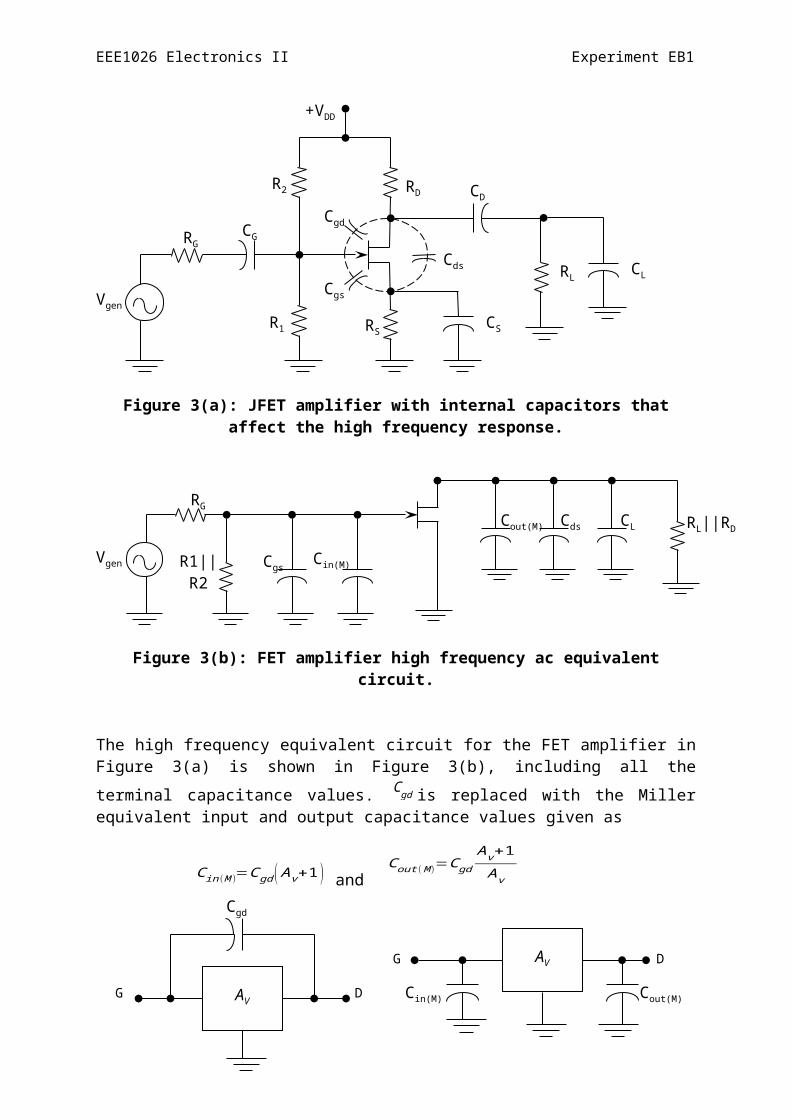
High Frequency Response of FET Amplifier
The high frequency response of the FET is limited by values of internal capacitance, as shown in Figure 3(a). There is a measurable amount of capacitance between each terminal pair of the FET. These capacitances each have a reactance that decreases as frequency increases. As the reactance of a given terminal capacitance decreases, more and more of the signal at the terminal is bypassed through the capacitance.
Vin
G
S
DVG
Vgen
RGCG
CS
CD
RD RL
RSR1||R2
RLRD
CD
gmVgs
D
S
VD
EEE1026 Electronics II Experiment EB1
Figure 3(a): JFET amplifier with internal capacitors that affect the high frequency response.
Figure 3(b): FET amplifier high frequency ac equivalent circuit.
The high frequency equivalent circuit for the FET amplifier in Figure 3(a) is shown in Figure
3(b), including all the terminal capacitance values. Cgd is replaced with the Miller equivalent input and output capacitance values given as
C in(M )=C gd ( Av+1 ) andCout (M )=Cgd
Av+1Av
Figure 4: Miller equivalent circuit for a feedback capacitor.
CL
+VDD
Vgen
Cds
Cgs
Cgd
RGCG
CS
CDRD
RL
R2
RSR1
RL||RDCLCds
Cgs Cin(M)Vgen
RG
Cout(M)
R1||R2
Cout(M)
DG
DG Cin(M)
AV
Cgd
AV
EEE1026 Electronics II Experiment EB1
Note the absence of capacitorsCG ,CD and CS in Figure 3(b), which are all assumed to be short circuit at high frequencies. From this figure, the gate and drain circuit capacitance are given by
CG' =Cgs+Cin( M ) and CD
' =Cout (M )+Cds+C L
whereCL is the input capacitance of the following stage. In general the capacitance Cgs is
the largest of the parasitic capacitances, with Cds the smallest. The high cutoff frequencies for the gate and drain circuits are then given by
f HG= 12 π Rin
' CG'
andf HD= 1
2 πR 'L CD'
whereRin' =RG||Rin and R 'L=RD||RL . At very high frequencies, the effect of CG
' is to
reduce the total impedance of the parallel combination ofR1 ,R2 and CG'
in Figure 3(b). The result is a reduced level of voltage across the gate-source terminals. Similarly, for the drain circuit, the capacitive reactance of CD
' will decrease with frequency and consequently
reduces the total impedance of the output parallel branches of Figure 3(b). It causes the output voltage to decrease as the reactance becomes smaller.
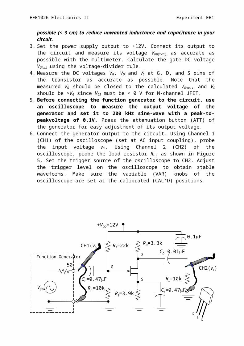
3.0 Procedures
1. Before connecting the circuit of Figure 5, measure the actual resistance of R1, R2, RD, RS
and RL as accurate as possible with a digital multimeter (set it to the best resistance range) and record the measured values.
2. Connect the common source JFET amplifier circuit as shown in Figure 5 using a breadboard (refer to Appendix C). Do not connect the power supply and the function generator to the circuit yet. Keep the connecting wires on the breadboard as short as possible (< 3 cm) to reduce unwanted inductance and capacitance in your circuit.
3. Set the power supply output to +12V. Connect its output to the circuit and measure its voltage VDD(meas) as accurate as possible with the multimeter. Calculate the gate DC voltage VG(cal) using the voltage-divider rule.
4. Measure the DC voltages VG, VD and VS at G, D, and S pins of the transistor as accurate as possible. Note that the measured VG should be closed to the calculated VG(cal), and VS
should be >VG since VGS must be < 0 V for N-channel JFET. 5. Before connecting the function generator to the circuit, use an oscilloscope to
measure the output voltage of the generator and set it to 200 kHz sine-wave with a peak-to-peakvoltage of 0.1V. Press the attenuation button (ATT) of the generator for easy adjustment of its output voltage.
6. Connect the generator output to the circuit. Using Channel 1 (CH1) of the oscilloscope (set at AC input coupling), probe the input voltage vin. Using Channel 2 (CH2) of the oscilloscope, probe the load resistor RL, as shown in Figure 5. Set the trigger source of the oscilloscope to CH2. Adjust the trigger level on the oscilloscope to obtain stable waveforms. Make sure the variable (VAR) knobs of the oscilloscope are set at the calibrated (CAL’D) positions.
EEE1026 Electronics II Experiment EB1
Figure 5: A Common source JFET amplifier
7. Adjust the Volts/div and Time/div to display the waveforms on the oscilloscope screen as big as possible with one to two cycles. Sketch the input AC voltage (vin) and the load voltage (vL) waveforms on the graph. Record the Time/div and Volts/div used. Note that the input and output waveforms should be approximately 180o out of phase.
8. From your graph, determine VL(pp) and Vin(pp) which are the peak-to-peak voltages of vL and vin, respectively. Calculate the voltage gain (Av) of the JFET amplifier circuit at 200 kHz. Ask the instructor to check all of your results. You must show the oscilloscope waveforms to the instructor.
9. Sweep the frequency of the function generator from 1 kHz to 550 kHz (use smaller frequency steps near the half-power point while larger steps can be used at mid-band frequencies). Record the peak-to-peak voltages of vin (CH1) and vL (CH2) and calculate the dB magnitude of the voltage gain Av. Use both coarse and fine adjustment knobs of the function generator for frequency adjustment.
10. Plot a curve of Av versus frequency.
GS
D
CH1(vin)
CH2(vL)
0.1F
S
D
G
Function Generator
RS=3.9k
RL=10k
CS=0.47F
CD=0.01F
RD=3.3k
R2 =10kVgen
50
CG=0.47F
R1=22k
+VDD=12V
The Resistor color code chart
ABC
AB x 10C pF
.abc
0.abcF
Capacitance
Potentiometer
A Var B
EEE1026 Electronics II Experiment EB1
APPENDIX A
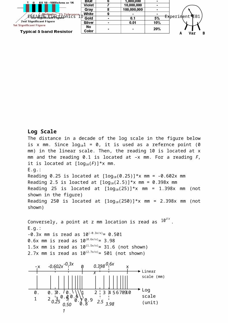
Log Scale The distance in a decade of the log scale in the figure below is x mm. Since log 101 = 0, it is used as a refernce point (0 mm) in the linear scale. Then, the reading 10 is located at x mm and the reading 0.1 is located at –x mm. For a reading F, it is located at [1og10(F)]*x mm. E.g.: Reading 0.25 is located at [1og10(0.25)]*x mm = -0.602x mmReading 2.5 is loacted at [1og10(2.5)]*x mm = 0.398x mmReading 25 is located at [1og10(25)]*x mm = 1.398x mm (not shown in the figure)Reading 250 is located at [1og10(250)]*x mm = 2.398x mm (not shown)
Conversely, a point at z mm location is read as 10z/ x.
E.g.: -0.3x mm is read as 10(-0.3x/x)= 0.5010.6x mm is read as 10(0.6x/x)= 3.981.5x mm is read as 10(1.5x/x)= 31.6 (not shown)2.7x mm is read as 10(2.7x/x)= 501 (not shown)
8764
0.90.8
0.70.60.4
-0.3x
0.501 3.98
0.6x-0.602x 0.398x
2.50.25
Log scale (unit)
Linear scale (mm)
x0-x
10 5 3210.50.30.20.1 9
EEE1026 Electronics II Experiment EB1

EEE1026 Electronics II Experiment EB
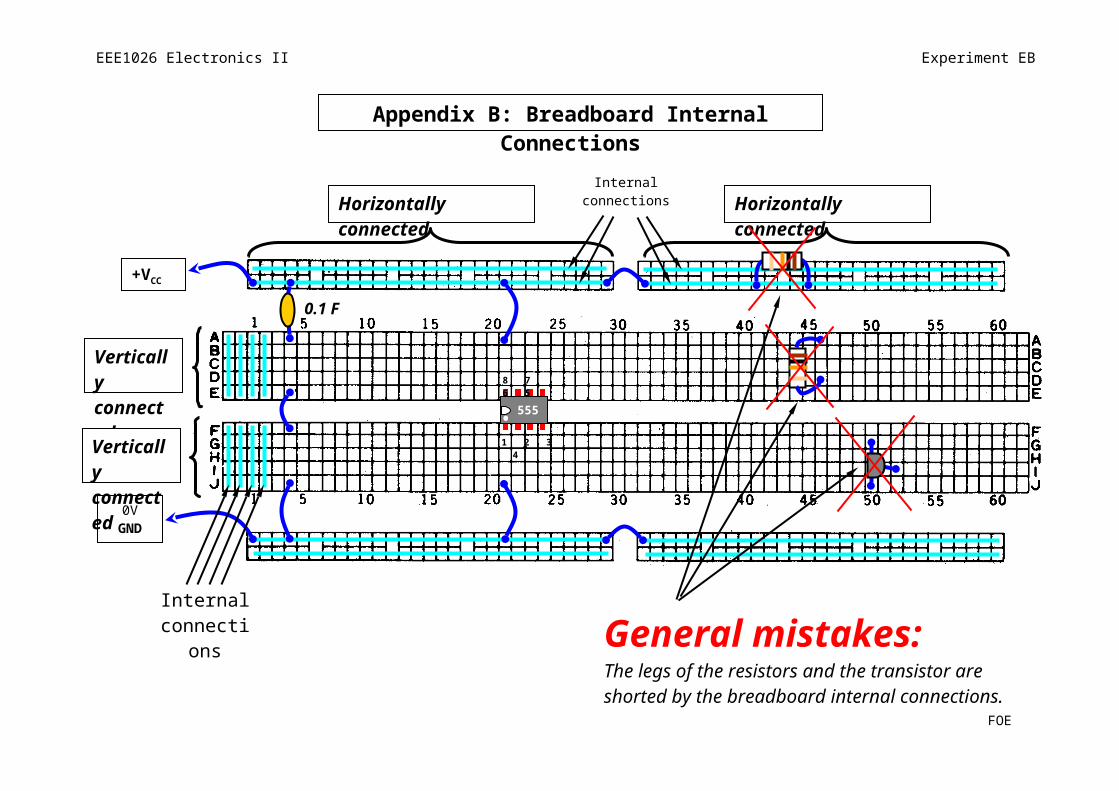
Internal connections
Internal connections
0.1 F
FOEMultimediaUniversity
General mistakes:The legs of the resistors and the transistor are shorted by the breadboard internal connections.
8 7 6 5
1 2 3 4
555
0VGND
+VCC
Horizontally connectedHorizontally connected
Vertically connected
Vertically connected
Appendix B: Breadboard Internal Connections
EEE1026 Electronics IIExperiment EB1: FET Amplifier Frequency Response
Lab Report(Together with Rubric form, Submit your report on the same day immediately after the
experiment)
Name: ________________________Student I.D.: _______________Date: __________
Majoring: ____________________ Group: ____________ Table No.: ____________
1. Table E1: Measured resistance valuesR1 R2 RD RS RL
3. VDD(meas) = ________ V, VG(cal) = ________ V
4. Table E2: Measured DC voltagesV G V D V S
7. Graph E1: vin and vL waveforms at 200 kHz
Time base : ______ s/div, CH1 (vin) : ______ V/div, CH2 (vL) : ______ V/div
8. Av=
V L( pp )
V in( pp )=
________ at 200 kHz
CH1 & CH2 groundCH1 & CH2 groundCH1 & CH2 groundCH1 & CH2 groundCH1 & CH2 groundCH1 & CH2 groundCH1 & CH2 groundCH1 & CH2 groundCH1 & CH2 groundCH1 & CH2 groundCH1 & CH2 ground

EEE1026 Electronics II Experiment EB1
9. Table E3: Measure VL(pp) and Vin(pp), and calculated AV
f /kHz 1 2 5 10 20 40 60 80 100 200 500 550VL(pp) /VVin(pp) /VAv(dB)
10. Graph E2: Av versus frequency
Signature: ______________ Time: ___________ Remarks _________________
Page: 2
EEE1026 Electronics II Experiment EB1
Discussion
1. Identify how the vin and vL waveforms in Step 7 are related in terms of positive and
negative peak voltages, waveform shapes and phase shift.
________________________________________________________________________
________________________________________________________________________
________________________________________________________________________
________________________________________________________________________
2. Describe the Av versus frequency characteristic.
________________________________________________________________________
________________________________________________________________________
________________________________________________________________________
________________________________________________________________________
Conclude your work by explaining why the frequency response analysis is important for
amplifiers.
___________________________________________________________________________
___________________________________________________________________________
___________________________________________________________________________
___________________________________________________________________________
___________________________________________________________________________
Page: 3

EEE1026 Electronics II Experiment EB
STUDENT'S NAME:ID NO:SUBJECT CODE AND TITLE: EEN1026 ELECTRONICS 2EXPERIMENT TITLE: EB1 - FET Amplifier Frequency ResponseEXPERIMENT DATE: TIME:
Criteria 1 (Need Improvement) 2 (Satisfactory) 3 (Good) 4 (Excellent) Rating Awarded by Assessor
Data Collection and Setting up the Experiment1 Ability to construct the
amplifier circuit on the breadboard
Unable to construct the amplifier circuit, and not asking for help.
Able to construct the amplifier circuit partially.
Able to construct the amplifier circuit.
Able to construct the amplifier circuit correctly, with neat and tidy placement of components and jumper wires
2 Ability to set-up the power supply for the circuit, the function generator to the amplifier and to connect the oscilloscope to display the waveform
Unable to setup the DC or AC input to the amplifier, and not asking for help.
Able to setup the DC and AC input to the amplifier partially.
DC and AC input to the amplifier is correctly setup.
DC and AC input to the amplifier is correctly setup and the waveforms are visible in the oscilloscope.
Analysis and Conclusions3 Ability to extract the
midband amplifier's characteristics.
No voltage gain is observed, and not asking for help.
No voltage gain is observed, but the waveforms are approximately at opposite phase.
Voltage gain is more than unity, with the input and output at approximately opposite phase.
The voltage gain is fair, with the input and output at opposite phase.
4 Ability to extract the amplifier's complete frequency response.
There is no difference between the low-, mid- and high-frequency response of the amplifier.
Minor differences between the low-, mid- and high-frequency response of the amplifier.
Low-, mid- and high-frequency response of the amplifier shows some difference.
Low-, mid- and high-frequency response of the amplifier is clearly seen on a graph.
5 Ability to answer the questions in by Oral Assessment
Not able to answer the question, no attempt was made to answer
Able to answer questions with some basics answers and demonstrate some attempts to refer to the text books, notes, lab sheet
Able to answer most part of the questions, with some explanations and elaborations and demonstrate some attempts to refer to text books, notes or lab sheet
Answered all correctly with proper explanations and elaborations, without a need to refer to any references.
Note: This form is to be attached together with the Lab results