Embed Size (px)
Citation preview
EXPERIMENT #3
TRANSISTOR BIASING
Bias (operating point) for a transistor is established by specifying the quiescent (D.C., no signal) values of
collector-emitter voltage VCEQ and collector current ICQ. Reliable operation of a transistor over a wide range of
temperatures requires that bias voltage and current remain stable. However, variations of reverse-bias collector
current ICO, and emitter-base junction voltage with temperature preclude stable bias unless external
compensating circuits are used. Bias stabilizing circuits may employ resistors, thermistors, diodes, etc.
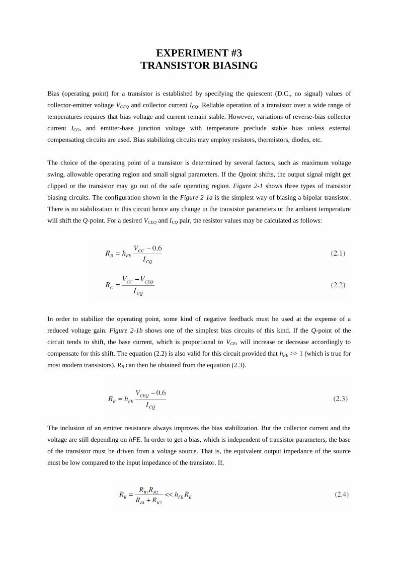
The choice of the operating point of a transistor is determined by several factors, such as maximum voltage
swing, allowable operating region and small signal parameters. If the Qpoint shifts, the output signal might get
clipped or the transistor may go out of the safe operating region. Figure 2-1 shows three types of transistor
biasing circuits. The configuration shown in the Figure 2-1a is the simplest way of biasing a bipolar transistor.
There is no stabilization in this circuit hence any change in the transistor parameters or the ambient temperature
will shift the Q-point. For a desired VCEQ and ICQ pair, the resistor values may be calculated as follows:
In order to stabilize the operating point, some kind of negative feedback must be used at the expense of a
reduced voltage gain. Figure 2-1b shows one of the simplest bias circuits of this kind. If the Q-point of the
circuit tends to shift, the base current, which is proportional to VCE, will increase or decrease accordingly to
compensate for this shift. The equation (2.2) is also valid for this circuit provided that hFE >> 1 (which is true for
most modern transistors). RB can then be obtained from the equation (2.3).
The inclusion of an emitter resistance always improves the bias stabilization. But the collector current and the
voltage are still depending on hFE. In order to get a bias, which is independent of transistor parameters, the base
of the transistor must be driven from a voltage source. That is, the equivalent output impedance of the source
must be low compared to the input impedance of the transistor. If,
this condition is satisfied in the circuit in the Figure 2-1c. The voltage source to drive the base is obtained using
voltage dividing resistors RB1, RB2. Assuming the bleeder current, I1, is ten times larger than the base current, IB
= IC / hFE, (this assumption usually satisfies the equation 2.4) the resistor values may be easily evaluated as
follows:
The quiescent voltages and currents of this circuit are quite independent of transistor parameters and temperature
and are functions of resistance values only.
EQUIPMENT
COMPONENTS
PROCEDURE
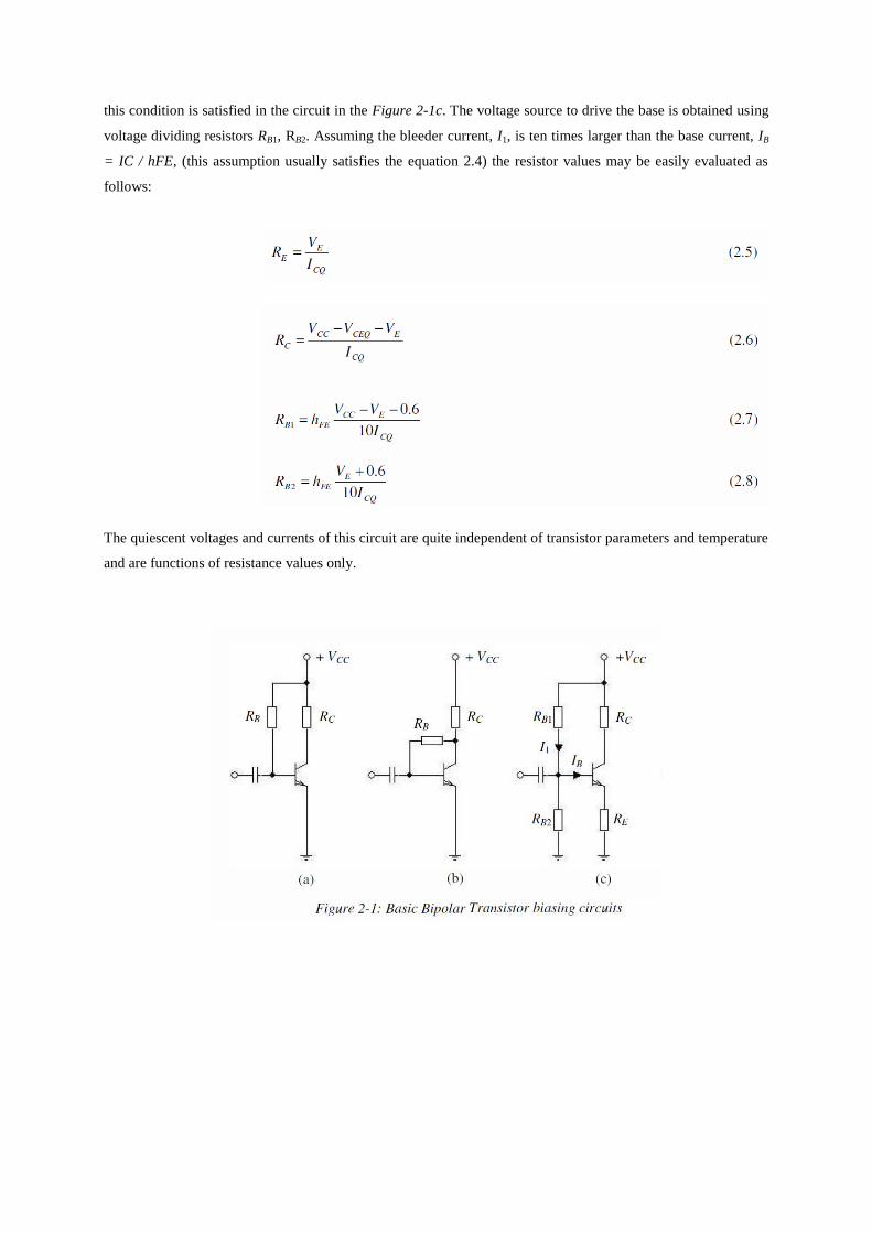
The first step in creating the data charts for measuring the BJT's characteristics is to construct a test circuit. Here,
we are using a simple circuit with only one resistor, two voltage supplies, an ammeter, and the BJT. The circuit
was constructed with the following schematic:
We will use three experimental trials, with a different Vs for each trial. Since the voltage drop across the Base-
Emitter junction is a constant 0.7 volts, the remainder of Vs must drop across the resistor. This allows us to find
the value of the base current. The resistor used was labeled 1 MΩ , but the real value was 997 KΩ. For each of
the three trials (VBE=20V, 25V and 30V), vary VCE between 0.02 volts and 20 volts and measure the resulting
collector current, IC. Fill the following table wih the data you collected.

Table 2.1
COLLECTOR CURRENT (IC)
VCE (Volts) VS=20 V VS=25 V VS=30 V
0.02
0.04
0.06
0.08
0.1
0.12
0.14
0.16
0.18
0.2
0.3
0.4
0.5
1.0
3.0
5.0
7.0
9.0
11.0
13.0
15.0
17.0
19.0
20.0

After finishing the first step continue with the following steps:

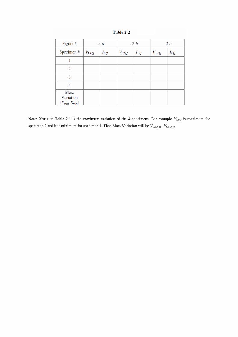
Note: Xmax in Table 2.1 is the maximum variation of the 4 specimens. For example VCEQ is maximum for
specimen 2 and it is minimum for specimen 4. Than Max. Variation will be VCEQ(2) - VCEQ(4).