Embed Size (px)
Citation preview
104 | TI-PMLK BUCK-WE Würth Elektronik
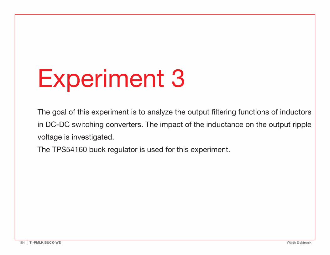
Experiment 3The goal of this experiment is to analyze the output filtering functions of inductors
in DC-DC switching converters. The impact of the inductance on the output ripple
voltage is investigated.
The TPS54160 buck regulator is used for this experiment.
105 | TI-PMLK BUCK-WE Würth Elektronik
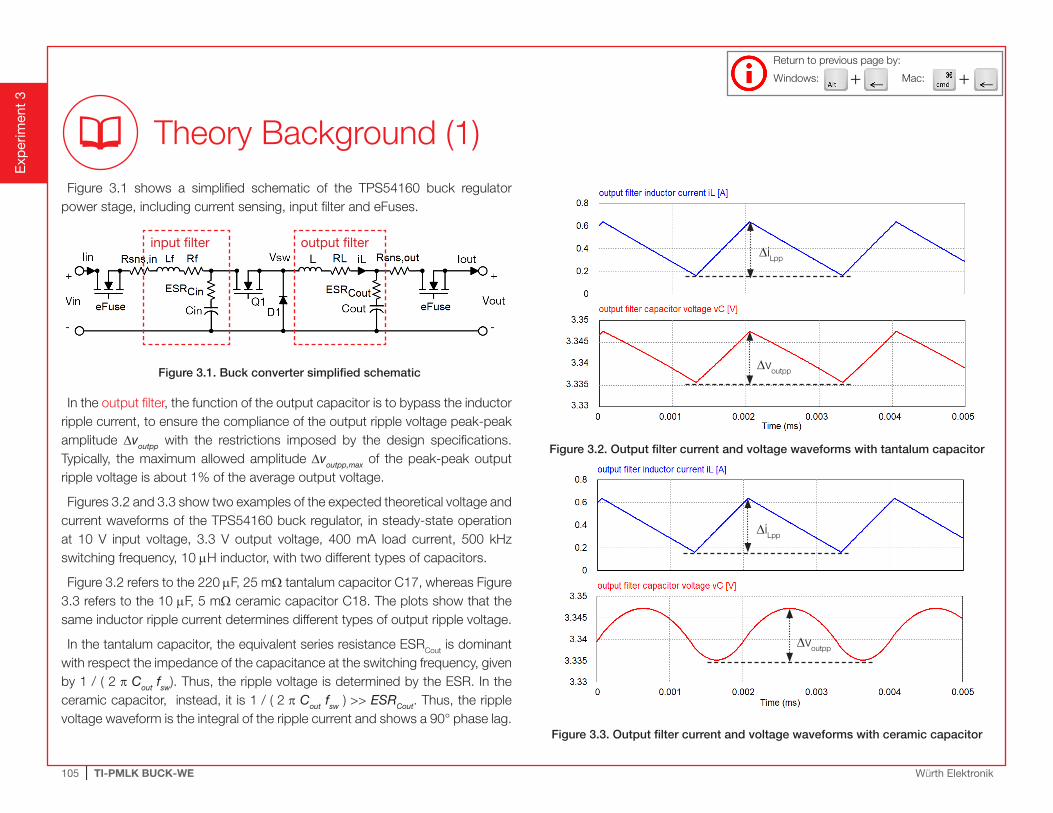
Figure 3.1 shows a simplified schematic of the TPS54160 buck regulator power stage, including current sensing, input filter and eFuses.
Figure 3.1. Buck converter simplified schematic
In the output filter, the function of the output capacitor is to bypass the inductor ripple current, to ensure the compliance of the output ripple voltage peak-peak amplitude Dvoutpp with the restrictions imposed by the design specifications. Typically, the maximum allowed amplitude Dvoutpp,max of the peak-peak output ripple voltage is about 1% of the average output voltage.
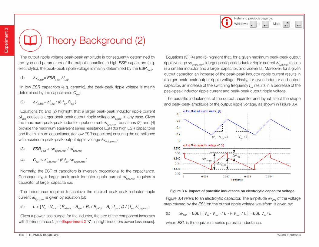
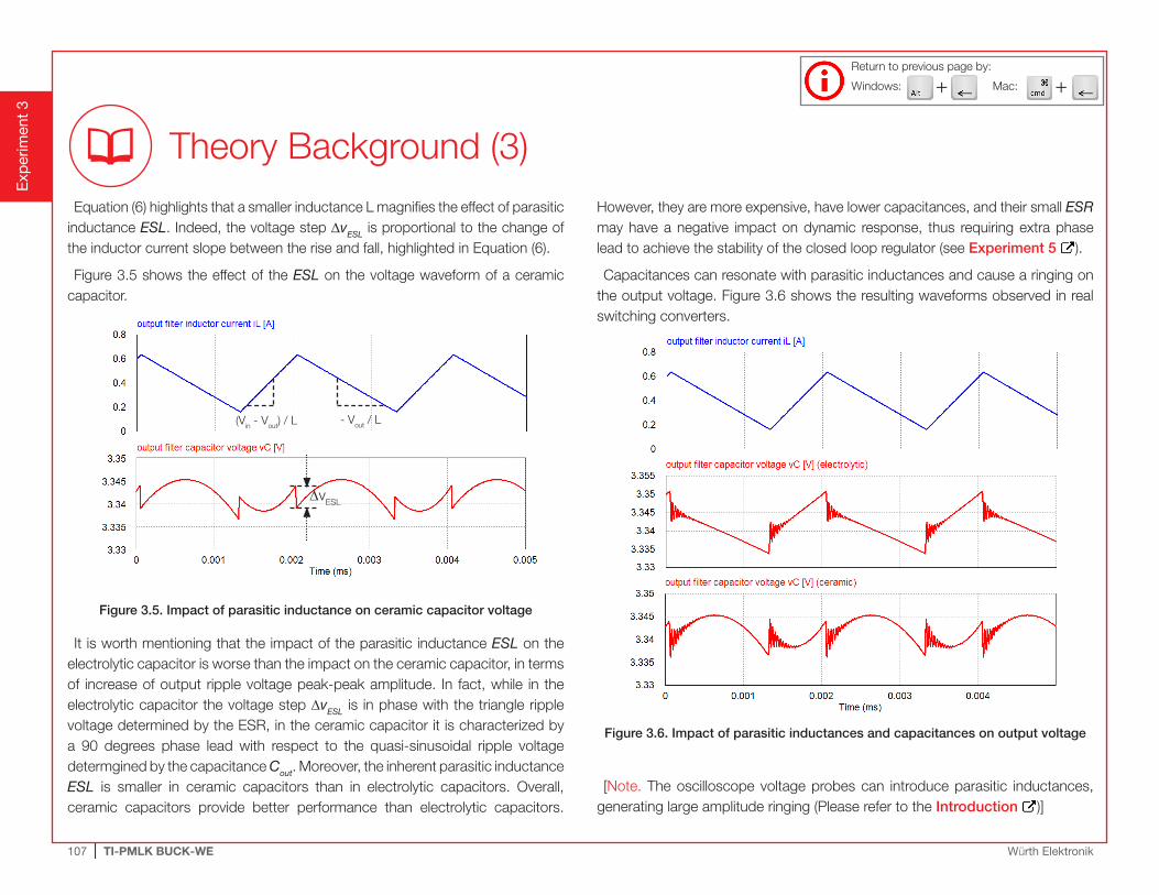
Figures 3.2 and 3.3 show two examples of the expected theoretical voltage and current waveforms of the TPS54160 buck regulator, in steady-state operation at 10 V input voltage, 3.3 V output voltage, 400 mA load current, 500 kHz switching frequency, 10 mH inductor, with two different types of capacitors.
Figure 3.2 refers to the 220 mF, 25 mW tantalum capacitor C17, whereas Figure 3.3 refers to the 10 mF, 5 mW ceramic capacitor C18. The plots show that the same inductor ripple current determines different types of output ripple voltage.
In the tantalum capacitor, the equivalent series resistance ESRCout is dominant with respect the impedance of the capacitance at the switching frequency, given by 1 / ( 2 p Cout fsw). Thus, the ripple voltage is determined by the ESR. In the ceramic capacitor, instead, it is 1 / ( 2 p Cout fsw ) >> ESRCout. Thus, the ripple voltage waveform is the integral of the ripple current and shows a 90° phase lag.
Figure 3.2. Output filter current and voltage waveforms with tantalum capacitor
Figure 3.3. Output filter current and voltage waveforms with ceramic capacitor
Exp
erim
ent
3
Theory Background (1)
DiLpp
Dvoutpp
input filter output filter
Dvoutpp
DiLpp
+ +Windows: Mac:
Return to previous page by:
106 | TI-PMLK BUCK-WE Würth Elektronik
The output ripple voltage peak-peak amplitude is consequently determined by the type and parameters of the output capacitor. In high ESR capacitors (e.g. electrolytic), the peak-peak ripple voltage is mainly determined by the ESRCout:
(1) Dvoutpp= ESRCout DiLpp
In low ESR capacitors (e.g. ceramic), the peak-peak ripple voltage is mainly determined by the capacitance Cout:
(2) Dvoutpp= DiLpp / (8 fsw Cout )
Equations (1) and (2) highlight that a larger peak-peak inductor ripple current DiLpp causes a larger peak-peak output ripple voltage Dvoutpp, in any case. Given the maximum peak-peak inductor ripple current DiLpp,max, equations (3) and (4) provide the maximum equivalent series resistance ESR (for high ESR capacitors) and the minimum capacitance (for low ESR capacitors) ensuring the compliance with maximum peak-peak output ripple voltage Dvoutpp,max:
(3) ESRCout < Dvoutpp,max / DiLpp,max
(4) Cout > DiLpp,max / (8 fsw Dvoutpp,max )
Normally, the ESR of capacitors is inversely proportional to the capacitance. Consequently, a larger peak-peak inductor ripple current DiLpp,max requires a capacitor of larger capacitance.
The inductance required to achieve the desired peak-peak inductor ripple current DiLpp,max is given by equation (5):
(5) L > [ Vin - Vout - ( ReFuse + Rsns + Rf + RMOS + RL ) Iout ] D / ( fsw DiLpp,max )
Given a power loss budget for the inductor, the size of the component increases with the inductance L [see Experiment 2 to insight inductors power loss issues].
Equations (3), (4) and (5) highlight that, for a given maximum peak-peak output ripple voltage Dvoutpp,max, a larger peak-peak inductor ripple current DiLpp,max results in a smaller inductor and a larger capacitor, and viceversa. Moreover, for a given output capacitor, an increase of the peak-peak inductor ripple current results in a larger peak-peak output ripple voltage. Finally, for given inductor and output capacitor, an increase of the switching frequency fsw results in a decrease of the peak-peak inductor ripple current and peak-peak output ripple voltage.
The parasitic inductances of the output capacitor and layout affect the shape and peak-peak amplitude of the output ripple voltage, as shown in Figure 3.4.
Figure 3.4. Impact of parasitic inductance on electrolytic capacitor voltage
Figure 3.4 refers to an electrolytic capacitor. The amplitude DvESL of the voltage step caused by the ESL on the output ripple voltage waveform is given by:
(6) DvESL = ESL [ ( Vin - Vout ) / L - (- Vout) / L ] = ESL Vin / L
where ESL is the equivalent series parasitic inductance.
Exp
erim
ent
3
Theory Background (2)
DvESL
(Vin - Vout) / L - Vout / L
DvoutppDvESR
+ +Windows: Mac:
Return to previous page by:
107 | TI-PMLK BUCK-WE Würth Elektronik
Equation (6) highlights that a smaller inductance L magnifies the effect of parasitic inductance ESL. Indeed, the voltage step DvESL is proportional to the change of the inductor current slope between the rise and fall, highlighted in Equation (6).
Figure 3.5 shows the effect of the ESL on the voltage waveform of a ceramic capacitor.
Figure 3.5. Impact of parasitic inductance on ceramic capacitor voltage
It is worth mentioning that the impact of the parasitic inductance ESL on the electrolytic capacitor is worse than the impact on the ceramic capacitor, in terms of increase of output ripple voltage peak-peak amplitude. In fact, while in the electrolytic capacitor the voltage step DvESL is in phase with the triangle ripple voltage determined by the ESR, in the ceramic capacitor it is characterized by a 90 degrees phase lead with respect to the quasi-sinusoidal ripple voltage determgined by the capacitance Cout. Moreover, the inherent parasitic inductance ESL is smaller in ceramic capacitors than in electrolytic capacitors. Overall, ceramic capacitors provide better performance than electrolytic capacitors.
However, they are more expensive, have lower capacitances, and their small ESR may have a negative impact on dynamic response, thus requiring extra phase lead to achieve the stability of the closed loop regulator (see Experiment 5 ).
Capacitances can resonate with parasitic inductances and cause a ringing on the output voltage. Figure 3.6 shows the resulting waveforms observed in real switching converters.
Figure 3.6. Impact of parasitic inductances and capacitances on output voltage
[Note. The oscilloscope voltage probes can introduce parasitic inductances, generating large amplitude ringing (Please refer to the Introduction )]
Exp
erim
ent
3
Theory Background (3)
DvESL
(Vin - Vout) / L - Vout / L
+ +Windows: Mac:
Return to previous page by:
108 | TI-PMLK BUCK-WE Würth Elektronik
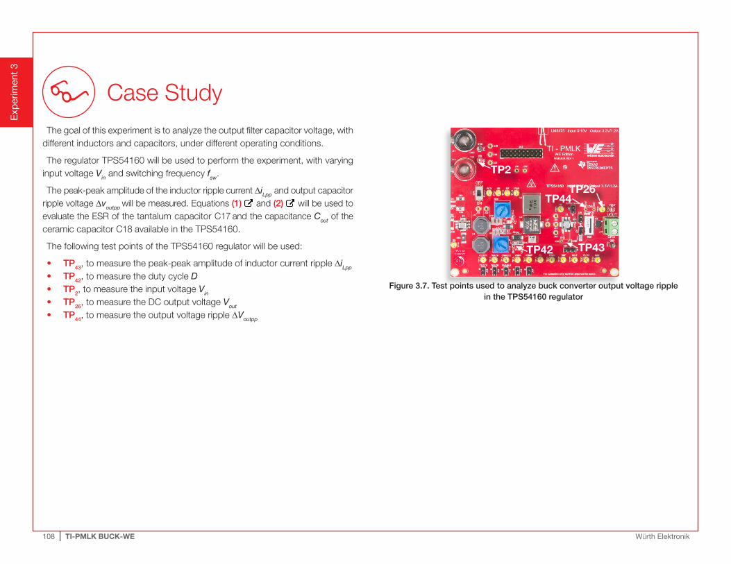
The goal of this experiment is to analyze the output filter capacitor voltage, with different inductors and capacitors, under different operating conditions.
The regulator TPS54160 will be used to perform the experiment, with varying input voltage Vin and switching frequency fsw.
The peak-peak amplitude of the inductor ripple current DiLpp and output capacitor ripple voltage Dvoutpp will be measured. Equations (1) and (2) will be used to evaluate the ESR of the tantalum capacitor C17 and the capacitance Cout of the ceramic capacitor C18 available in the TPS54160.
The following test points of the TPS54160 regulator will be used:
• TP43, to measure the peak-peak amplitude of inductor current ripple DiLpp
• TP42, to measure the duty cycle D• TP2, to measure the input voltage Vin
• TP26, to measure the DC output voltage Vout
• TP44, to measure the output voltage ripple DVoutpp
Figure 3.7. Test points used to analyze buck converter output voltage ripple in the TPS54160 regulator
Exp
erim
ent
3
Case Study
TP2
TP43TP42
TP26TP44
109 | TI-PMLK BUCK-WE Würth Elektronik
Experiment set-up: configuration
Exp
erim
ent
3
VO
LTA
GE
PR
OB
E 2
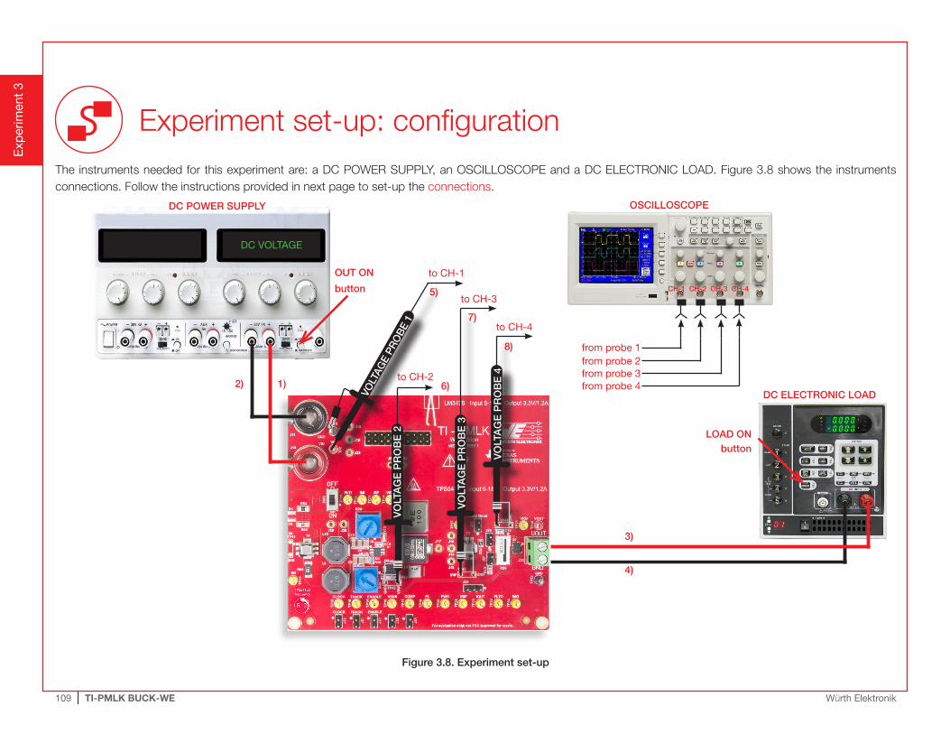
The instruments needed for this experiment are: a DC POWER SUPPLY, an OSCILLOSCOPE and a DC ELECTRONIC LOAD. Figure 3.8 shows the instruments connections. Follow the instructions provided in next page to set-up the connections.
Figure 3.8. Experiment set-up
DC POWER SUPPLY
DC VOLTAGE
OUT ON
button
to CH-21)
CH-1 CH-2 CH-3 CH-4
OSCILLOSCOPE
from probe 1
2)
4)
5)
6)
7)
8)
DC ELECTRONIC LOAD
LOAD ON button
to CH-1
to CH-3
to CH-4
from probe 2from probe 3from probe 4
3)
VOLT
AGE
PRO
BE
1
VO
LTA
GE
PR
OB
E 3
VO
LTA
GE
PR
OB
E 4
110 | TI-PMLK BUCK-WE Würth Elektronik
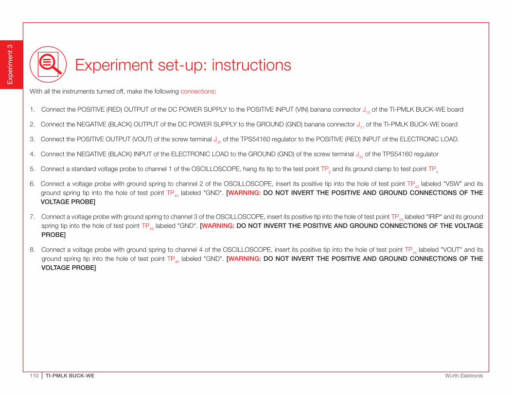
Experiment set-up: instructionsWith all the instruments turned off, make the following connections:
1. Connect the POSITIVE (RED) OUTPUT of the DC POWER SUPPLY to the POSITIVE INPUT (VIN) banana connector J10 of the TI-PMLK BUCK-WE board
2. Connect the NEGATIVE (BLACK) OUTPUT of the DC POWER SUPPLY to the GROUND (GND) banana connector J11 of the TI-PMLK BUCK-WE board
3. Connect the POSITIVE OUTPUT (VOUT) of the screw terminal J32 of the TPS54160 regulator to the POSITIVE (RED) INPUT of the ELECTRONIC LOAD.
4. Connect the NEGATIVE (BLACK) INPUT of the ELECTRONIC LOAD to the GROUND (GND) of the screw terminal J32 of the TPS54160 regulator
5. Connect a standard voltage probe to channel 1 of the OSCILLOSCOPE, hang its tip to the test point TP2 and its ground clamp to test point TP4
6. Connect a voltage probe with ground spring to channel 2 of the OSCILLOSCOPE, insert its positive tip into the hole of test point TP42 labeled "VSW" and itsground spring tip into the hole of test point TP42 labeled "GND". [WARNING: DO NOT INVERT THE POSITIVE AND GROUND CONNECTIONS OF THEVOLTAGE PROBE]
7. Connect a voltage probe with ground spring to channel 3 of the OSCILLOSCOPE, insert its positive tip into the hole of test point TP43 labeled "IRIP" and its groundspring tip into the hole of test point TP43 labeled "GND". [WARNING: DO NOT INVERT THE POSITIVE AND GROUND CONNECTIONS OF THE VOLTAGEPROBE]
8. Connect a voltage probe with ground spring to channel 4 of the OSCILLOSCOPE, insert its positive tip into the hole of test point TP44 labeled "VOUT" and itsground spring tip into the hole of test point TP44 labeled "GND". [WARNING: DO NOT INVERT THE POSITIVE AND GROUND CONNECTIONS OF THEVOLTAGE PROBE]
Exp
erim
ent
3
111 | TI-PMLK BUCK-WE Würth Elektronik
Test#1: instructions (1)
Exp
erim
ent
3
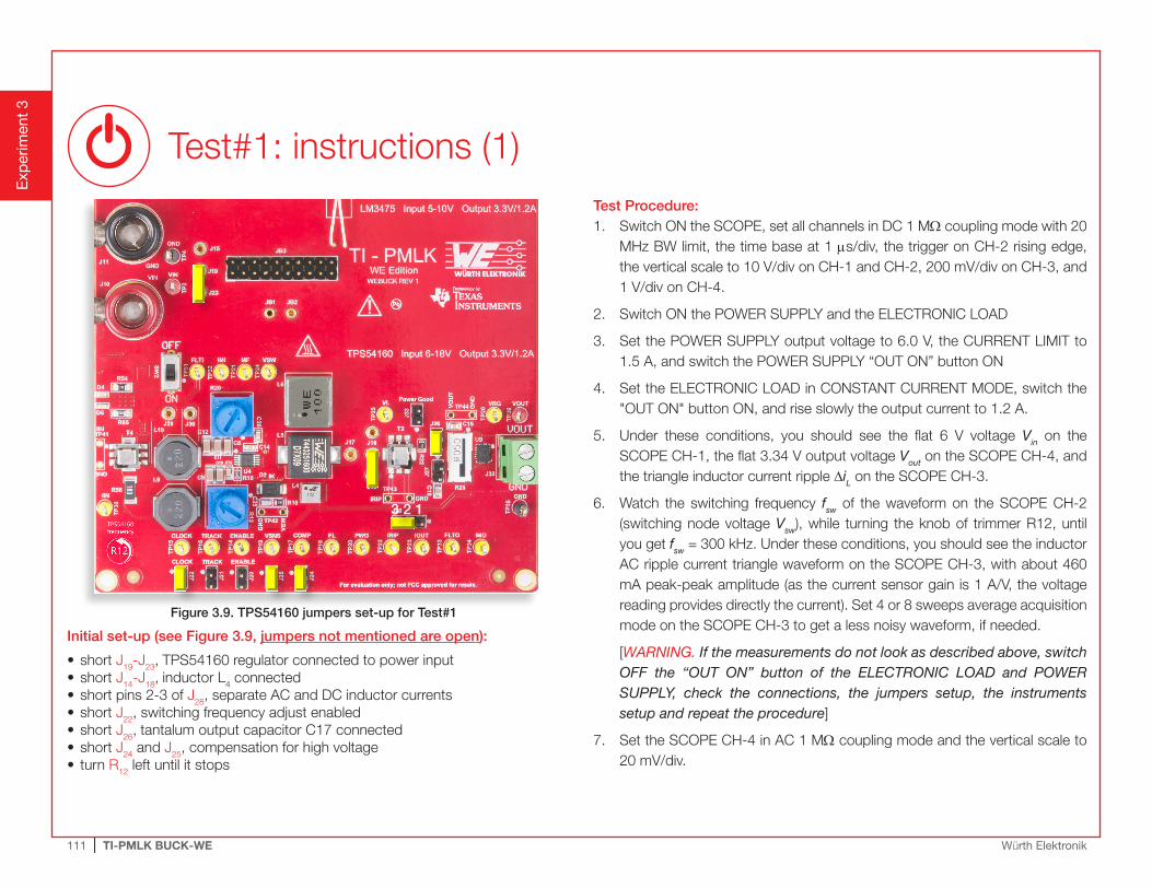
Figure 3.9. TPS54160 jumpers set-up for Test#1
Initial set-up (see Figure 3.9, jumpers not mentioned are open):
• short J19-J23, TPS54160 regulator connected to power input• short J14-J18, inductor L4 connected• short pins 2-3 of J28, separate AC and DC inductor currents• short J22, switching frequency adjust enabled• short J26, tantalum output capacitor C17 connected• short J24 and J25, compensation for high voltage• turn R12 left until it stops
Test Procedure:1. Switch ON the SCOPE, set all channels in DC 1 MW coupling mode with 20
MHz BW limit, the time base at 1 ms/div, the trigger on CH-2 rising edge,the vertical scale to 10 V/div on CH-1 and CH-2, 200 mV/div on CH-3, and1 V/div on CH-4.
2. Switch ON the POWER SUPPLY and the ELECTRONIC LOAD
3. Set the POWER SUPPLY output voltage to 6.0 V, the CURRENT LIMIT to1.5 A, and switch the POWER SUPPLY “OUT ON” button ON
4. Set the ELECTRONIC LOAD in CONSTANT CURRENT MODE, switch the"OUT ON" button ON, and rise slowly the output current to 1.2 A.
5. Under these conditions, you should see the flat 6 V voltage Vin on theSCOPE CH-1, the flat 3.34 V output voltage Vout on the SCOPE CH-4, andthe triangle inductor current ripple DiL on the SCOPE CH-3.
6. Watch the switching frequency fsw of the waveform on the SCOPE CH-2(switching node voltage Vsw), while turning the knob of trimmer R12, untilyou get fsw = 300 kHz. Under these conditions, you should see the inductorAC ripple current triangle waveform on the SCOPE CH-3, with about 460mA peak-peak amplitude (as the current sensor gain is 1 A/V, the voltagereading provides directly the current). Set 4 or 8 sweeps average acquisitionmode on the SCOPE CH-3 to get a less noisy waveform, if needed.
[WARNING. If the measurements do not look as described above, switchOFF the “OUT ON” button of the ELECTRONIC LOAD and POWERSUPPLY, check the connections, the jumpers setup, the instrumentssetup and repeat the procedure]
7. Set the SCOPE CH-4 in AC 1 MW coupling mode and the vertical scale to20 mV/div.
3 2 1
112 | TI-PMLK BUCK-WE Würth Elektronik
8. Check the DC POWER SUPPLY, and adjust it by using the fine regulationknob, if needed.
9. Measure the amplitude of the peak-peak inductor ripple current DiLpp on theSCOPE CH-3, and record the measured values in Table 3.1.
10. Measure the amplitude of the peak-peak output voltage ripple voltage Dvoutpp
on the SCOPE CH-4, and record the measured values in Table 3.1.
11. Measure the amplitude of the ESL step voltage DvESL on the SCOPE CH-4(see Figure 3.10 and 3.11), and record the measured values in Table 3.1.
12. Repeat the steps 8 to 11, by increasing the input voltage of 3 V steps, upto 18 V.
13. Watch the switching frequency fsw of the waveform on the SCOPE CH-2,while turning the knob of trimmer R12, until you get fsw = 450 kHz, and adjustthe POWER SUPPLY voltage until you read 6 V on the SCOPE CH-1.
14. Repeat the steps 8 to 12.
15. Reduce the current of the ELECTRONIC LOAD to 0.0 A, switch its “LOADON” button OFF, and switch the POWER SUPPLY “OUT ON” button OFF.
16. Short J14-J17 to connect the inductor L5, repeat the steps 3 to 14, andrecord the measurement results in Table 3.2.
17. Reduce the current of the ELECTRONIC LOAD to 0.0 A, switch its “LOADON” button OFF, and switch the POWER SUPPLY “OUT ON” button OFF.
18. Switch the ELECTRONIC LOAD and the POWER SUPPLY OFF.
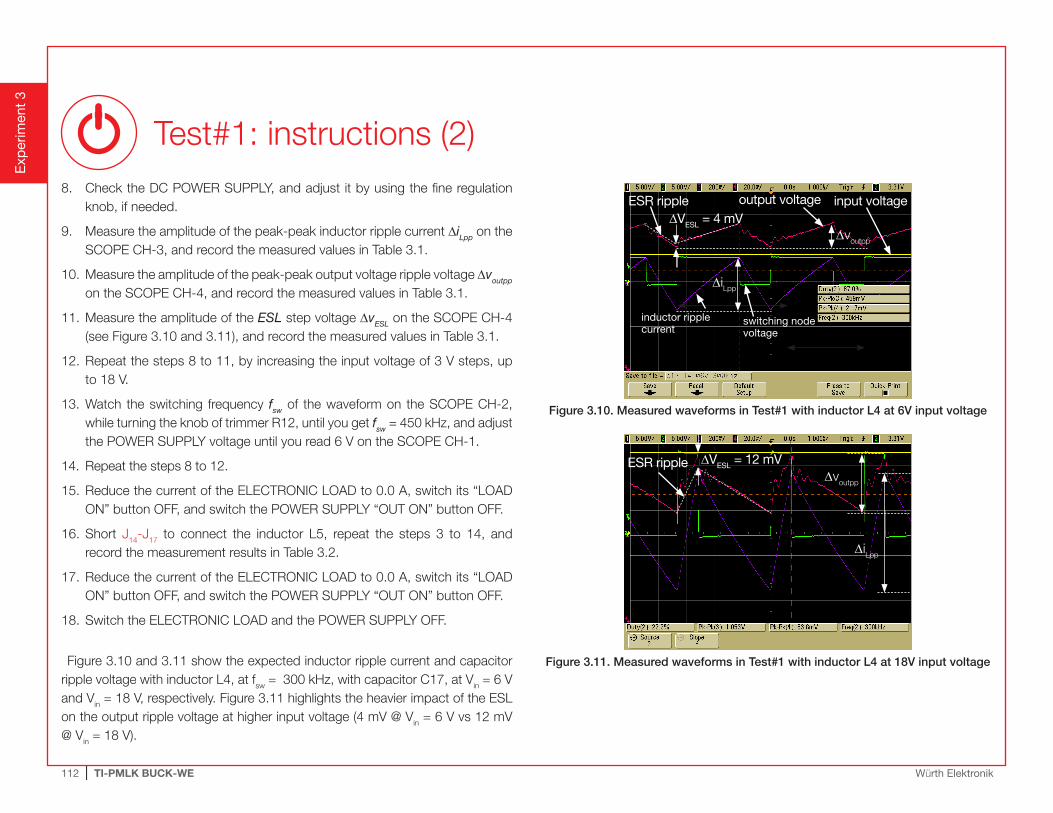
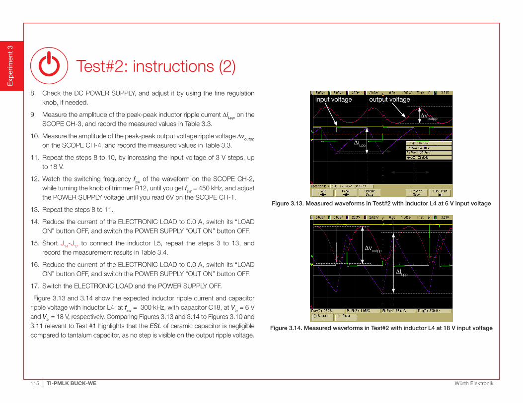
Figure 3.10 and 3.11 show the expected inductor ripple current and capacitor ripple voltage with inductor L4, at fsw = 300 kHz, with capacitor C17, at Vin = 6 V and Vin = 18 V, respectively. Figure 3.11 highlights the heavier impact of the ESL on the output ripple voltage at higher input voltage (4 mV @ Vin = 6 V vs 12 mV @ Vin = 18 V).
inductor ripple current
switching nodevoltage
output voltage input voltage
Dvoutpp
DiLpp
ESR rippleDVESL = 4 mV
Figure 3.10. Measured waveforms in Test#1 with inductor L4 at 6V input voltage
Dvoutpp
DiLpp
ESR ripple DVESL = 12 mV
Figure 3.11. Measured waveforms in Test#1 with inductor L4 at 18V input voltage
Test#1: instructions (2)
Exp
erim
ent
3
113 | TI-PMLK BUCK-WE Würth Elektronik
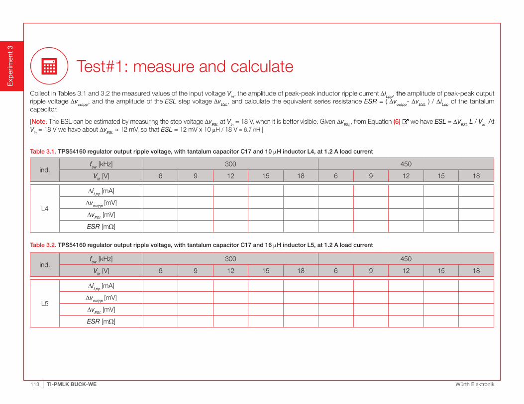
Test#1: measure and calculateCollect in Tables 3.1 and 3.2 the measured values of the input voltage Vin, the amplitude of peak-peak inductor ripple current DiLpp, the amplitude of peak-peak output ripple voltage Dvoutpp, and the amplitude of the ESL step voltage DvESL, and calculate the equivalent series resistance ESR = ( Dvoutpp- DvESL ) / DiLpp of the tantalum capacitor.
[Note. The ESL can be estimated by measuring the step voltage DvESL at Vin = 18 V, when it is better visible. Given DvESL, from Equation (6) we have ESL = DVESL L / Vin. At Vin = 18 V we have about DvESL ≈ 12 mV, so that ESL = 12 mV x 10 mH / 18 V ≈ 6.7 nH.]
Table 3.1. TPS54160 regulator output ripple voltage, with tantalum capacitor C17 and 10 mH inductor L4, at 1.2 A load current
ind.fsw [kHz] 300 450
Vin [V] 6 9 12 15 18 6 9 12 15 18
L4
DiLpp [mA]
Dvoutpp [mV]
DvESL [mV]
ESR [mW]
Table 3.2. TPS54160 regulator output ripple voltage, with tantalum capacitor C17 and 16 mH inductor L5, at 1.2 A load current
ind.fsw [kHz] 300 450
Vin [V] 6 9 12 15 18 6 9 12 15 18
L5
DiLpp [mA]
Dvoutpp [mV]
DvESL [mV]
ESR [mW]
Exp
erim
ent
3
114 | TI-PMLK BUCK-WE Würth Elektronik
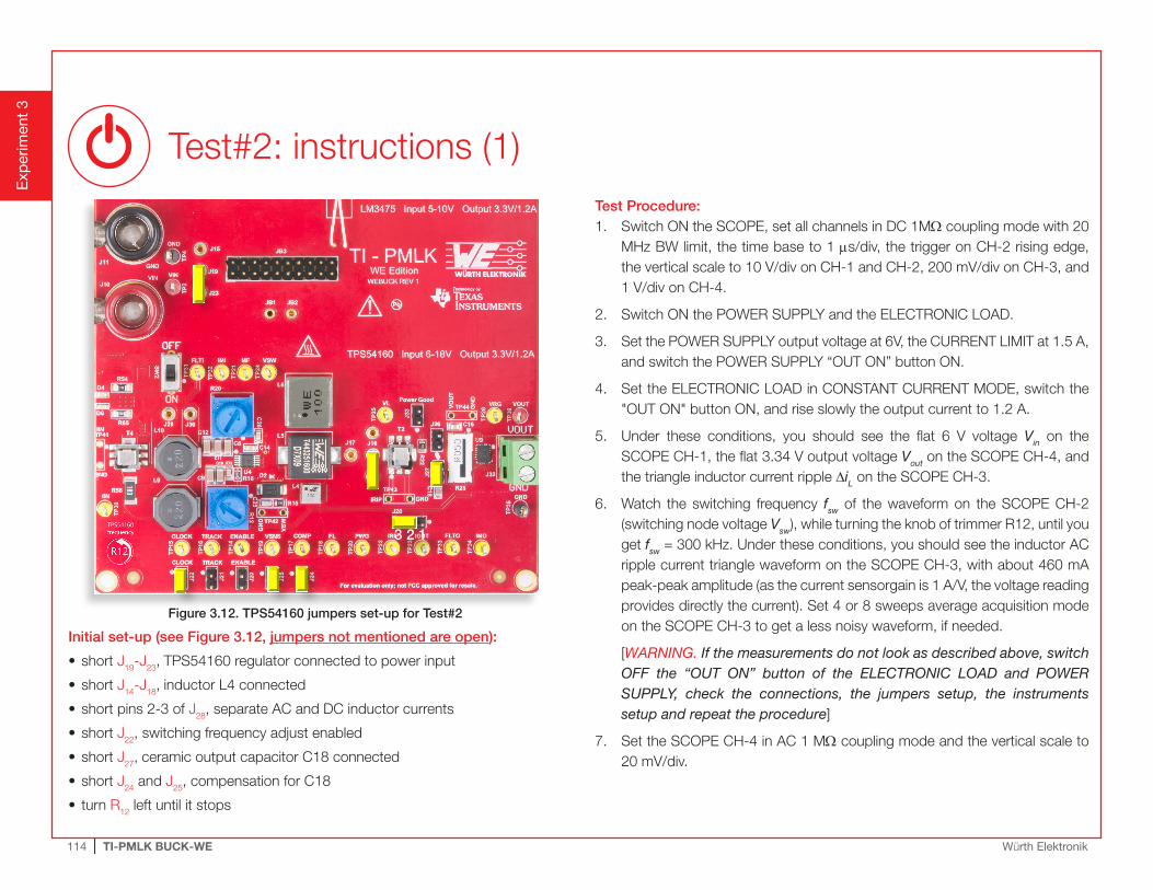
Test#2: instructions (1)
Exp
erim
ent
3
Figure 3.12. TPS54160 jumpers set-up for Test#2
Initial set-up (see Figure 3.12, jumpers not mentioned are open):
• short J19-J23, TPS54160 regulator connected to power input
• short J14-J18, inductor L4 connected
• short pins 2-3 of J28, separate AC and DC inductor currents
• short J22, switching frequency adjust enabled
• short J27, ceramic output capacitor C18 connected
• short J24 and J25, compensation for C18
• turn R12 left until it stops
Test Procedure:1. Switch ON the SCOPE, set all channels in DC 1MW coupling mode with 20
MHz BW limit, the time base to 1 ms/div, the trigger on CH-2 rising edge,the vertical scale to 10 V/div on CH-1 and CH-2, 200 mV/div on CH-3, and1 V/div on CH-4.
2. Switch ON the POWER SUPPLY and the ELECTRONIC LOAD.
3. Set the POWER SUPPLY output voltage at 6V, the CURRENT LIMIT at 1.5 A,and switch the POWER SUPPLY “OUT ON” button ON.
4. Set the ELECTRONIC LOAD in CONSTANT CURRENT MODE, switch the"OUT ON" button ON, and rise slowly the output current to 1.2 A.
5. Under these conditions, you should see the flat 6 V voltage Vin on theSCOPE CH-1, the flat 3.34 V output voltage Vout on the SCOPE CH-4, andthe triangle inductor current ripple DiL on the SCOPE CH-3.
6. Watch the switching frequency fsw of the waveform on the SCOPE CH-2(switching node voltage Vsw), while turning the knob of trimmer R12, until youget fsw = 300 kHz. Under these conditions, you should see the inductor ACripple current triangle waveform on the SCOPE CH-3, with about 460 mApeak-peak amplitude (as the current sensorgain is 1 A/V, the voltage readingprovides directly the current). Set 4 or 8 sweeps average acquisition modeon the SCOPE CH-3 to get a less noisy waveform, if needed.
[WARNING. If the measurements do not look as described above, switchOFF the “OUT ON” button of the ELECTRONIC LOAD and POWERSUPPLY, check the connections, the jumpers setup, the instrumentssetup and repeat the procedure]
7. Set the SCOPE CH-4 in AC 1 MW coupling mode and the vertical scale to20 mV/div.
3 2 1
115 | TI-PMLK BUCK-WE Würth Elektronik
8. Check the DC POWER SUPPLY, and adjust it by using the fine regulationknob, if needed.
9. Measure the amplitude of the peak-peak inductor ripple current DiLpp on theSCOPE CH-3, and record the measured values in Table 3.3.
10. Measure the amplitude of the peak-peak output voltage ripple voltage Dvoutpp
on the SCOPE CH-4, and record the measured values in Table 3.3.
11. Repeat the steps 8 to 10, by increasing the input voltage of 3 V steps, upto 18 V.
12. Watch the switching frequency fsw of the waveform on the SCOPE CH-2,while turning the knob of trimmer R12, until you get fsw = 450 kHz, and adjustthe POWER SUPPLY voltage until you read 6V on the SCOPE CH-1.
13. Repeat the steps 8 to 11.
14. Reduce the current of the ELECTRONIC LOAD to 0.0 A, switch its “LOADON” button OFF, and switch the POWER SUPPLY “OUT ON” button OFF.
15. Short J14-J17 to connect the inductor L5, repeat the steps 3 to 13, andrecord the measurement results in Table 3.4.
16. Reduce the current of the ELECTRONIC LOAD to 0.0 A, switch its “LOADON” button OFF, and switch the POWER SUPPLY “OUT ON” button OFF.
17. Switch the ELECTRONIC LOAD and the POWER SUPPLY OFF.
Figure 3.13 and 3.14 show the expected inductor ripple current and capacitor ripple voltage with inductor L4, at fsw = 300 kHz, with capacitor C18, at Vin = 6 V and Vin = 18 V, respectively. Comparing Figures 3.13 and 3.14 to Figures 3.10 and 3.11 relevant to Test #1 highlights that the ESL of ceramic capacitor is negligible compared to tantalum capacitor, as no step is visible on the output ripple voltage.
Figure 3.13. Measured waveforms in Test#2 with inductor L4 at 6 V input voltage
Figure 3.14. Measured waveforms in Test#2 with inductor L4 at 18 V input voltage
Test#2: instructions (2)
Exp
erim
ent
3
input voltage
Dvoutpp
DiLpp
output voltage
Dvoutpp
DiLpp
116 | TI-PMLK BUCK-WE Würth Elektronik
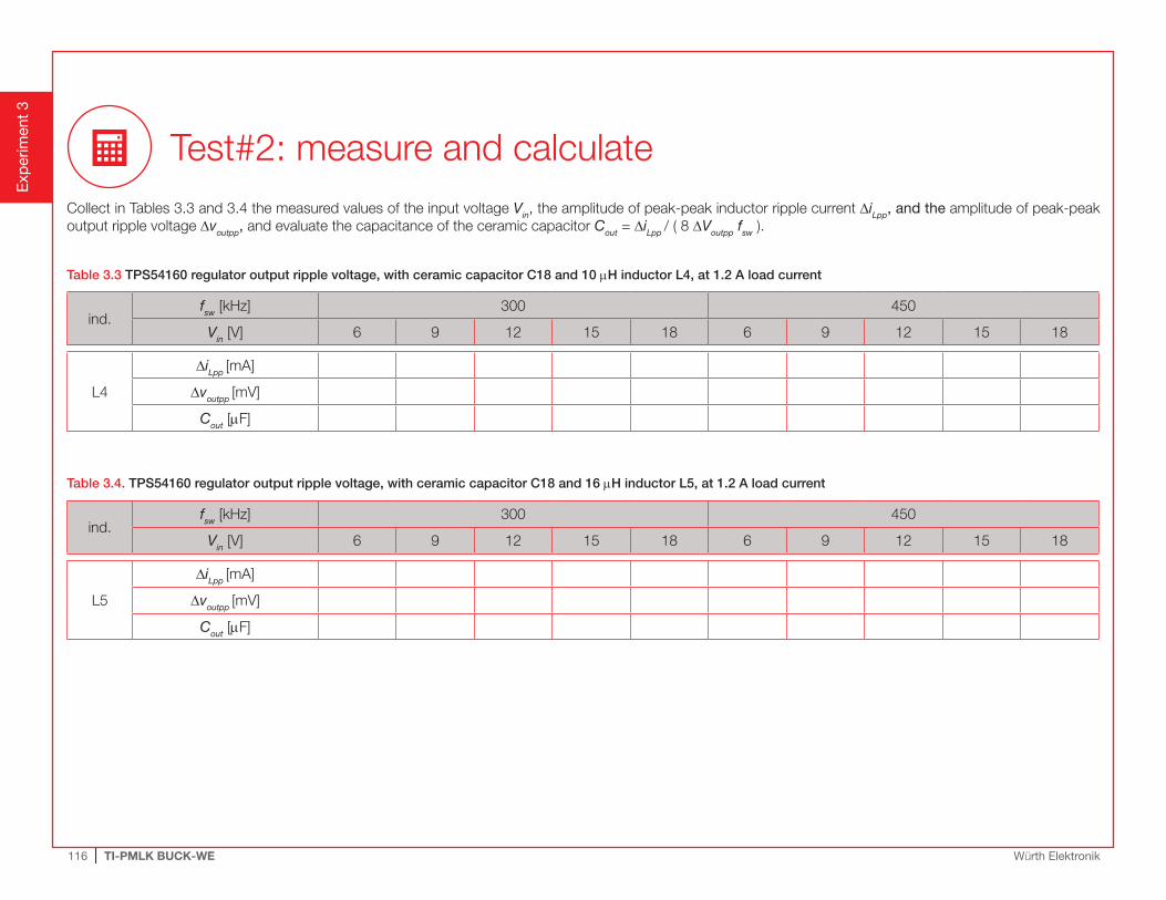
Test#2: measure and calculateCollect in Tables 3.3 and 3.4 the measured values of the input voltage Vin, the amplitude of peak-peak inductor ripple current DiLpp, and the amplitude of peak-peak output ripple voltage Dvoutpp, and evaluate the capacitance of the ceramic capacitor Cout = DiLpp / ( 8 DVoutpp fsw ).
Table 3.3 TPS54160 regulator output ripple voltage, with ceramic capacitor C18 and 10 mH inductor L4, at 1.2 A load current
ind.fsw [kHz] 300 450
Vin [V] 6 9 12 15 18 6 9 12 15 18
L4
DiLpp [mA]
Dvoutpp [mV]
Cout [mF]
Table 3.4. TPS54160 regulator output ripple voltage, with ceramic capacitor C18 and 16 mH inductor L5, at 1.2 A load current
ind.fsw [kHz] 300 450
Vin [V] 6 9 12 15 18 6 9 12 15 18
L5
DiLpp [mA]
Dvoutpp [mV]
Cout [mF]
Exp
erim
ent
3
117 | TI-PMLK BUCK-WE Würth Elektronik
1 How does the peak-peak amplitude of the output ripple voltage vary as the input voltage increases?
it increases it decreases other: _____________________________________________________
Please comment your answer: ________________________________________________________________________________________________________________
____________________________________________________________________________________________________________________________________________
2 How do the inductors influence the peak-peak amplitude of the output ripple voltage?
the amplitude is larger with L4 the amplitude is larger with L5 other: _____________________________________________________
Please comment your answer: ________________________________________________________________________________________________________________
____________________________________________________________________________________________________________________________________________
3 How does the switching frequency fsw influence the peak-peak amplitude of the output ripple voltage?
the amplitude is larger with higher fsw the amplitude is larger with lower fsw other: _____________________________________________________
Please comment your answer: ________________________________________________________________________________________________________________
____________________________________________________________________________________________________________________________________________
4 How does the capacitor influence the peak-peak amplitude of the output ripple voltage?
the amplitude is larger with C17 the amplitude is larger with C18 other: _____________________________________________________
Please comment your answer: ________________________________________________________________________________________________________________
____________________________________________________________________________________________________________________________________________
Exp
erim
ent
3
Observe and Answer?
118 | TI-PMLK BUCK-WE Würth Elektronik
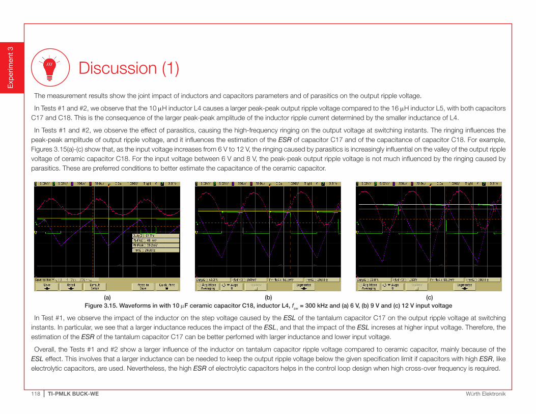
Discussion (1)The measurement results show the joint impact of inductors and capacitors parameters and of parasitics on the output ripple voltage.
In Tests #1 and #2, we observe that the 10 mH inductor L4 causes a larger peak-peak output ripple voltage compared to the 16 mH inductor L5, with both capacitors C17 and C18. This is the consequence of the larger peak-peak amplitude of the inductor ripple current determined by the smaller inductance of L4.
In Tests #1 and #2, we observe the effect of parasitics, causing the high-frequency ringing on the output voltage at switching instants. The ringing influences the peak-peak amplitude of output ripple voltage, and it influences the estimation of the ESR of capacitor C17 and of the capacitance of capacitor C18. For example, Figures 3.15(a)-(c) show that, as the input voltage increases from 6 V to 12 V, the ringing caused by parasitics is increasingly influential on the valley of the output ripple voltage of ceramic capacitor C18. For the input voltage between 6 V and 8 V, the peak-peak output ripple voltage is not much influenced by the ringing caused by parasitics. These are preferred conditions to better estimate the capacitance of the ceramic capacitor.
(a) (b) (c)Figure 3.15. Waveforms in with 10 mF ceramic capacitor C18, inductor L4, fsw = 300 kHz and (a) 6 V, (b) 9 V and (c) 12 V input voltage
In Test #1, we observe the impact of the inductor on the step voltage caused by the ESL of the tantalum capacitor C17 on the output ripple voltage at switching instants. In particular, we see that a larger inductance reduces the impact of the ESL, and that the impact of the ESL increses at higher input voltage. Therefore, the estimation of the ESR of the tantalum capacitor C17 can be better perfomed with larger inductance and lower input voltage.
Overall, the Tests #1 and #2 show a larger influence of the inductor on tantalum capacitor ripple voltage compared to ceramic capacitor, mainly because of the ESL effect. This involves that a larger inductance can be needed to keep the output ripple voltage below the given specification limit if capacitors with high ESR, like electrolytic capacitors, are used. Nevertheless, the high ESR of electrolytic capacitors helps in the control loop design when high cross-over frequency is required.
Exp
erim
ent
3
119 | TI-PMLK BUCK-WE Würth Elektronik
Figure 3.16. Impedance and ESR of capacitor C18 vs frequency
Figure 3.17. Capacitance de-rating of capacitor C18 vs DC bias voltage
Figure 3.18. Capacitance de-rating of capacitor C18 vs temperature
Figure 3.19. Temperature rise of capacitor C18 vs ripple current
Exp
erim
ent
3
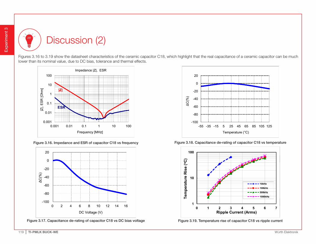
Figures 3.16 to 3.19 show the datasheet characteristics of the ceramic capacitor C18, which highlight that the real capacitance of a ceramic capacitor can be much lower than its nominal value, due to DC bias, tolerance and thermal effects.
Discussion (2)
120 | TI-PMLK BUCK-WE Würth Elektronik
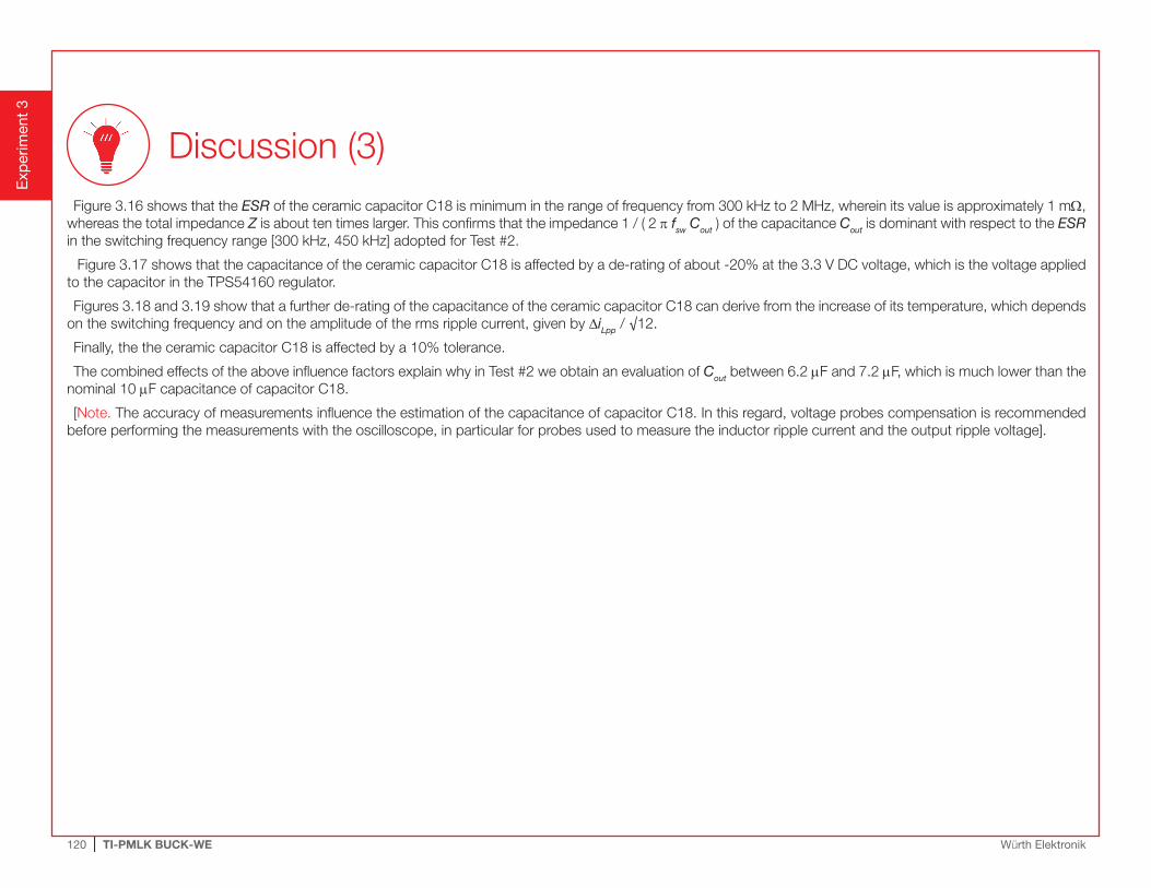
Figure 3.16 shows that the ESR of the ceramic capacitor C18 is minimum in the range of frequency from 300 kHz to 2 MHz, wherein its value is approximately 1 mW, whereas the total impedance Z is about ten times larger. This confirms that the impedance 1 / ( 2 p fsw Cout ) of the capacitance Cout is dominant with respect to the ESR in the switching frequency range [300 kHz, 450 kHz] adopted for Test #2.
Figure 3.17 shows that the capacitance of the ceramic capacitor C18 is affected by a de-rating of about -20% at the 3.3 V DC voltage, which is the voltage applied to the capacitor in the TPS54160 regulator.
Figures 3.18 and 3.19 show that a further de-rating of the capacitance of the ceramic capacitor C18 can derive from the increase of its temperature, which depends on the switching frequency and on the amplitude of the rms ripple current, given by DiLpp / √12.
Finally, the the ceramic capacitor C18 is affected by a 10% tolerance.
The combined effects of the above influence factors explain why in Test #2 we obtain an evaluation of Cout between 6.2 mF and 7.2 mF, which is much lower than the nominal 10 mF capacitance of capacitor C18.
[Note. The accuracy of measurements influence the estimation of the capacitance of capacitor C18. In this regard, voltage probes compensation is recommended before performing the measurements with the oscilloscope, in particular for probes used to measure the inductor ripple current and the output ripple voltage].
Exp
erim
ent
3
Discussion (3)
121 | TI-PMLK BUCK-WE Würth Elektronik
Expansion Activities
Exp
erim
ent
3
• Repeat the experiment with inductor L6 of TPS54160 regulator.
• Repeat the experiment with TPS54160 load current lower than 1.2 A.
[Note. 1) The TPS54160 can operate in discontinuous conduction mode at high input voltage and low load current. The ripple current and ripple voltage equationsare different. 2) The TPS54160 regulator features a skip-cycle mode, determining an automatic reduction of switching frequency at low load current. This mayresult in discontinuous conduction mode operation. 3) See Experiment 5 to investigate the impact of inductors on discontinuous conduction mode].
• Repeat the experiment with LM3475 regulator.
122 | TI-PMLK BUCK-WE Würth Elektronik
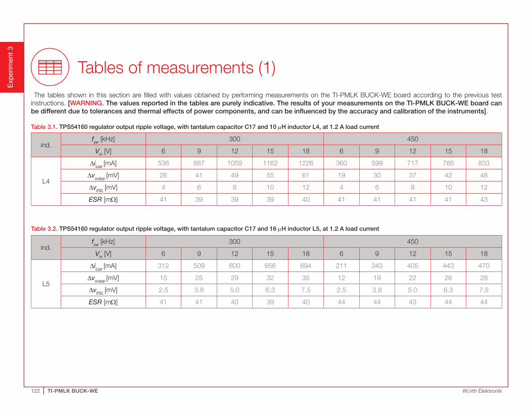
Tables of measurements (1)
Exp
erim
ent
3
The tables shown in this section are filled with values obtained by performing measurements on the TI-PMLK BUCK-WE board according to the previous test instructions. [WARNING. The values reported in the tables are purely indicative. The results of your measurements on the TI-PMLK BUCK-WE board can be different due to tolerances and thermal effects of power components, and can be influenced by the accuracy and calibration of the instruments].
Table 3.1. TPS54160 regulator output ripple voltage, with tantalum capacitor C17 and 10 mH inductor L4, at 1.2 A load current
ind.fsw [kHz] 300 450
Vin [V] 6 9 12 15 18 6 9 12 15 18
L4
DiLpp [mA] 536 887 1059 1162 1226 360 599 717 785 833
Dvoutpp [mV] 26 41 49 55 61 19 30 37 42 48
DvESL [mV] 4 6 8 10 12 4 6 8 10 12
ESR [mW] 41 39 39 39 40 41 41 41 41 43
Table 3.2. TPS54160 regulator output ripple voltage, with tantalum capacitor C17 and 16 mH inductor L5, at 1.2 A load current
ind.fsw [kHz] 300 450
Vin [V] 6 9 12 15 18 6 9 12 15 18
L5
DiLpp [mA] 312 509 600 656 694 211 343 405 443 470
Dvoutpp [mV] 15 25 29 32 35 12 19 22 26 28
DvESL [mV] 2.5 3.8 5.0 6.3 7.5 2.5 3.8 5.0 6.3 7.5
ESR [mW] 41 41 40 39 40 44 44 43 44 44
123 | TI-PMLK BUCK-WE Würth Elektronik
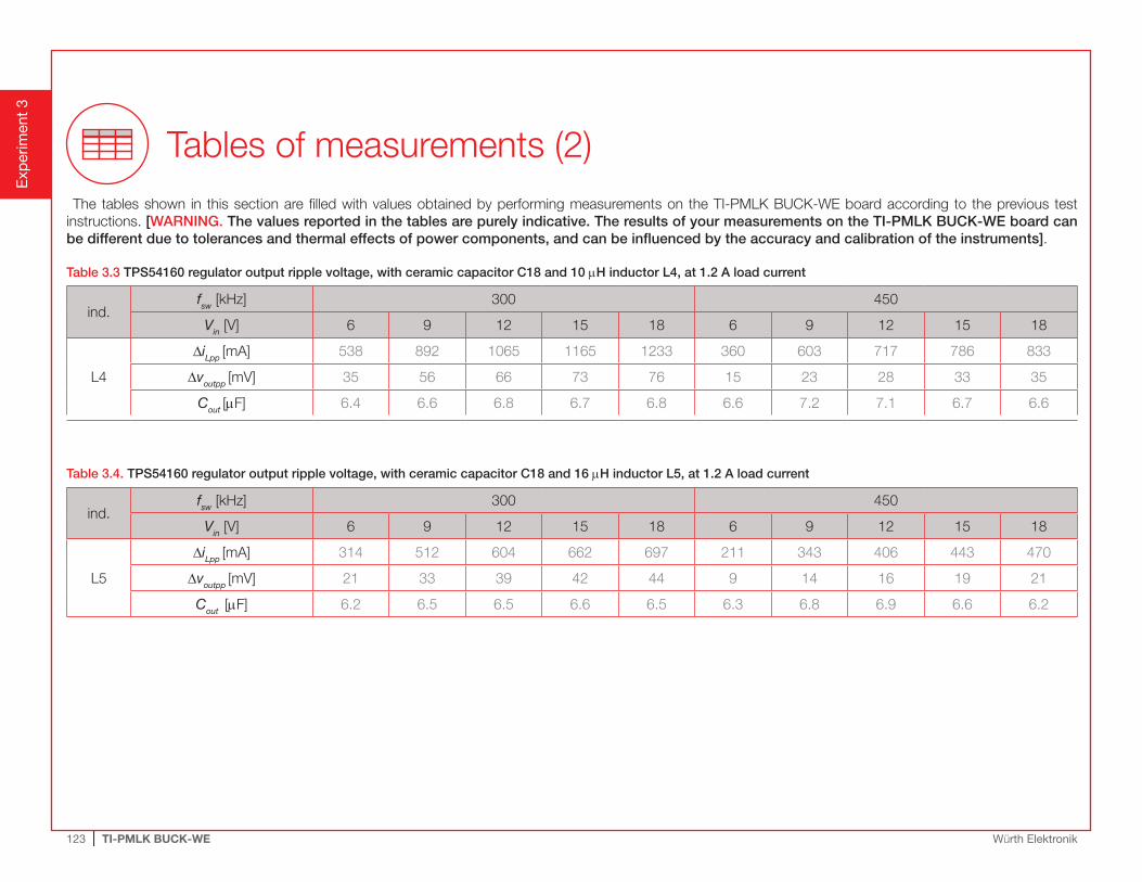
Tables of measurements (2)
Exp
erim
ent
3
The tables shown in this section are filled with values obtained by performing measurements on the TI-PMLK BUCK-WE board according to the previous test instructions. [WARNING. The values reported in the tables are purely indicative. The results of your measurements on the TI-PMLK BUCK-WE board can be different due to tolerances and thermal effects of power components, and can be influenced by the accuracy and calibration of the instruments].
Table 3.3 TPS54160 regulator output ripple voltage, with ceramic capacitor C18 and 10 mH inductor L4, at 1.2 A load current
ind.fsw [kHz] 300 450
Vin [V] 6 9 12 15 18 6 9 12 15 18
L4
DiLpp [mA] 538 892 1065 1165 1233 360 603 717 786 833
Dvoutpp [mV] 35 56 66 73 76 15 23 28 33 35
Cout [mF] 6.4 6.6 6.8 6.7 6.8 6.6 7.2 7.1 6.7 6.6
Table 3.4. TPS54160 regulator output ripple voltage, with ceramic capacitor C18 and 16 mH inductor L5, at 1.2 A load current
ind.fsw [kHz] 300 450
Vin [V] 6 9 12 15 18 6 9 12 15 18
L5
DiLpp [mA] 314 512 604 662 697 211 343 406 443 470
Dvoutpp [mV] 21 33 39 42 44 9 14 16 19 21
Cout [mF] 6.2 6.5 6.5 6.6 6.5 6.3 6.8 6.9 6.6 6.2