Embed Size (px)
Citation preview
A-DS-EXCARMD-01.0
Embedded Processors PLDs
Excalibur ARM-Based
101 Innovation DriveSan Jose, CA 95134(408) 544-7000http://www.altera.com
Hardware Reference ManualJanuary 2001
Version 1.0
ii Altera Corporation
ARM-Based Embedded Processor PLDs Hardware Reference Manual
Altera, APEX, ClockBoost, ClockLock, ClockShift, Excalibur, FineLine BGA, MegaCore, MegaWizard, NativeLink, Quartus, and SignalTap aretrademarks and/or service marks of Altera Corporation in the United States and other countries. Altera acknowledges the trademarks of otherorganizations for their respective products or services mentioned in this document, including the following: ARM, Thumb and the ARM-Powered logoare registered trademarks of ARM Limited. Altera products are protected under numerous U.S. and foreign patents and pending applications,maskwork rights, and copyrights. Altera warrants performance of its semiconductor products to current specifications inaccordance with Altera’s standard warranty, but reserves the right to make changes to any products and services at any timewithout notice. Altera assumes no responsibility or liability arising out of the application or use of any information, product, orservice described herein except as expressly agreed to in writing by Altera Corporation. Altera customers are advised to obtain thelatest version of device specifications before relying on any published information and before placing orders for products orservices.
Copyright 2001 Altera Corporation. All rights reserved.
ARM-Based EmbeddedProcessor PLDs
ContentsHardware Reference Manual
PRELIM
INARY IN
FORMAT
ION
Features... ..........................................................................................................................................7... & More Features ...........................................................................................................................8General Description .......................................................................................................................10Functional Description ..................................................................................................................12
ARM-Based Embedded Processor .......................................................................................12PLD Interfaces ........................................................................................................................13PLLs .........................................................................................................................................13External Memory Controllers ..............................................................................................14Peripherals ..............................................................................................................................15
Registers ..........................................................................................................................................15Memory Map ..................................................................................................................................15
Memory Mapping in Boot-From-Flash Mode ...................................................................16Memory Map Control Registers ..........................................................................................16
Embedded Processor .....................................................................................................................19ETM9 ........................................................................................................................................21Embedded Processor Debug Lines ......................................................................................23Embedded Processor Debug Pins ........................................................................................23Table 8 lists the debug pins. .................................................................................................23PLD Clocks ..............................................................................................................................24
Bus Architecture .............................................................................................................................24AHB1 Bus ................................................................................................................................26AHB2 Bus ................................................................................................................................28AHB Bridges ...........................................................................................................................31
Clocks ...............................................................................................................................................42External Reference .................................................................................................................42PLLs .........................................................................................................................................42Clock Control ..........................................................................................................................43Registers ..................................................................................................................................44
Configuration Logic .......................................................................................................................50Boot from Flash ......................................................................................................................50Boot from External Configuration Source ..........................................................................52Registers ..................................................................................................................................54
Interrupt Controller .......................................................................................................................56IRQ and FIQ Requests to the Processor ..............................................................................58Interrupt Priority ....................................................................................................................58Indirect Access to FIQ and IRQ ...........................................................................................59Operating Modes ...................................................................................................................60Interrupt Signals .....................................................................................................................62Registers ..................................................................................................................................63
Altera Corporation iii
Contents ARM-Based Embedded Processor PLD Hardware Reference Manual
PRELIM
INARY IN
FORMAT
ION
Expansion Bus Interface ................................................................................................................68Interface Signals .....................................................................................................................69EBI Operation .........................................................................................................................70AHB Slave Interface ...............................................................................................................71EBI Transaction Sequencer ...................................................................................................71Clocking ...................................................................................................................................77Connecting External Devices to the EBI .............................................................................77Registers ..................................................................................................................................77
SDRAM Controller ........................................................................................................................81Module I/O .............................................................................................................................82Bus Interface ...........................................................................................................................83Endianness ..............................................................................................................................83Arbitration ...............................................................................................................................85Memory Access State Machine ............................................................................................85Registers ..................................................................................................................................86SDRAM Device Configuration .............................................................................................89Clocking ...................................................................................................................................91
On-Chip SRAM ..............................................................................................................................92Single-Port SRAM Block .......................................................................................................92Registers ..................................................................................................................................94Dual-Port SRAM Block ..........................................................................................................95Registers ................................................................................................................................103
Reset and Mode Control .............................................................................................................105Types of Reset .......................................................................................................................105Sources of Reset ....................................................................................................................106Reset Operation ....................................................................................................................109Registers ................................................................................................................................110
Watchdog Timer ...........................................................................................................................112Interface Signals ...................................................................................................................112Counter Operation ...............................................................................................................112Trigger Modes ......................................................................................................................113Reloading the Watchdog Timer .........................................................................................113Software Locking .................................................................................................................114Reset .......................................................................................................................................114Registers ................................................................................................................................114
Timer ..............................................................................................................................................116Registers ................................................................................................................................118
UART .............................................................................................................................................121UART Pins and Signals .......................................................................................................122Transmitter Operation .........................................................................................................123Receiver Operation ..............................................................................................................123Modem Status Lines ............................................................................................................124UART Data Formats ............................................................................................................124Registers ................................................................................................................................125
Debug Support .............................................................................................................................133JTAG support ........................................................................................................................133
iv Altera Corporation
ARM-Based Embedded Processor PLD Hardware Reference Manual Contents
PRELIM
INARY IN
FORMAT
ION
SignalTap Embedded Logic Analyzer ..............................................................................135IEEE Std. 1149.1 (JTAG) Boundary-Scan Support ...........................................................135
I/O Features .................................................................................................................................137I/O Control ...........................................................................................................................137Registers ................................................................................................................................137New I/O Features ................................................................................................................139I/O Standards .......................................................................................................................139
Operating Conditions ..................................................................................................................142Electrical Characteristics & Timing Diagrams .........................................................................144
EBI Electrical Characteristics ..............................................................................................144SDRAM Electrical Characteristics .....................................................................................150Trace Electrical Characteristics ..........................................................................................159UART Electrical Characteristics .........................................................................................160JTAG Electrical Characteristics ..........................................................................................161Dual-Port SRAM Electrical Characteristics ......................................................................162Master Port and Slave Port electrical Characteristics .....................................................164
Device Pinouts ..............................................................................................................................164Packaging ......................................................................................................................................164Embedded Processor Register Summary .................................................................................165Abbreviations ...............................................................................................................................172Glossary .........................................................................................................................................174Comprehensive Pin & Signal Listing ........................................................................................178
Altera Corporation v

Notes:
PRELIM
INARY IN
FORMAT
ION
ARM-Based EmbeddedProcessor PLDs
Hardware Reference Manual
PRELIM
INARY IN
FORMAT
ION
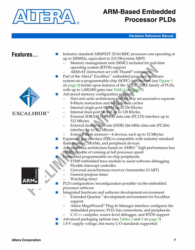
Features... Industry-standard ARM922T 32-bit RISC processor core operating at up to 200MHz, equivalent to 210 Dhrystone MIPS– Memory management unit (MMU) included for real-time
operating system (RTOS) support– ARMv4T instruction set with Thumb® extensions
Part of the Altera® Excalibur™ embedded processor solutions: system-on-a-programmable-chip (SOPC) architecture (see Figure 1 on page 4) builds upon features of the APEX™ 20KE family of PLDs, with up to 1,000,000 gates (see Table 1 on page 2)
Advanced memory configuration support– Harvard cache architecture with 64-way set associative separate
8-Kbyte instruction and 8-Kbyte data caches– Internal single-port SRAM up to 256 Kbytes– Internal dual-port SRAM up to 128 Kbytes– External SDRAM 133-MHz data rate (PC133) interface up to
512 Mbytes– External double-data rate (DDR) 266-MHz data rate (PC266)
interface up to 512 Mbytes– External flash memory—4 devices, each up to 32 Mbytes
Expansion bus interface (EBI) is compatible with industry-standard flash memory, SRAMs, and peripheral devices
Advanced bus architecture based on AMBA™ high-performance bus (AHB) capable of running at full processor speed
Embedded programmable on-chip peripherals– ETM9 embedded trace module to assist software debugging– Flexible interrupt controller– Universal asynchronous receiver/transmitter (UART)– General-purpose timer– Watchdog timer
PLD configuration/reconfiguration possible via the embedded processor software
Integrated hardware and software development environment– Extended Quartus™ development environment for Excalibur
support– Altera MegaWizard® Plug-In Manager interface configures the
embedded processor, PLD, bus connections, and peripherals– C/C++ compiler, source-level debugger, and RTOS support
Advanced packaging options (see Tables 2 and 3 on page 3) 1.8-V supply voltage, but many I/O standards supported
Altera Corporation 7
ARM-Based Embedded Processor PLDs Hardware Reference Manual
PRELIM
INARY IN
FORMAT
ION
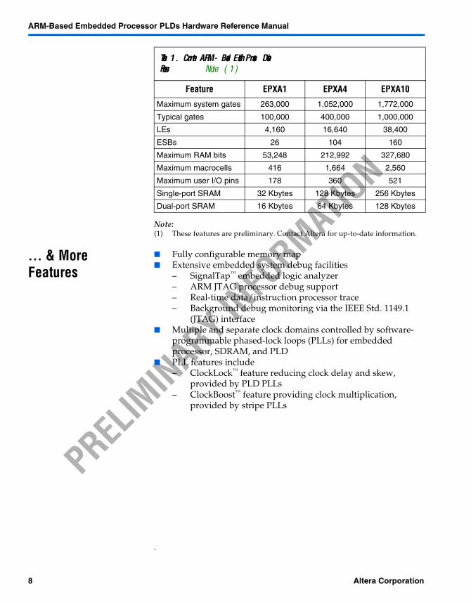
Note:(1) These features are preliminary. Contact Altera for up-to-date information.
... & More Features
Fully configurable memory map Extensive embedded system debug facilities
– SignalTap™ embedded logic analyzer– ARM JTAG processor debug support– Real-time data/instruction processor trace– Background debug monitoring via the IEEE Std. 1149.1
(JTAG) interface Multiple and separate clock domains controlled by software-
programmable phased-lock loops (PLLs) for embedded processor, SDRAM, and PLD
PLL features include– ClockLock™ feature reducing clock delay and skew,
provided by PLD PLLs– ClockBoost™ feature providing clock multiplication,
provided by stripe PLLs
.
Table 1. Current ARM-Based Embedded Processor Device Features Note (1)
Feature EPXA1 EPXA4 EPXA10
Maximum system gates 263,000 1,052,000 1,772,000
Typical gates 100,000 400,000 1,000,000
LEs 4,160 16,640 38,400
ESBs 26 104 160
Maximum RAM bits 53,248 212,992 327,680
Maximum macrocells 416 1,664 2,560
Maximum user I/O pins 178 360 521
Single-port SRAM 32 Kbytes 128 Kbytes 256 Kbytes
Dual-port SRAM 16 Kbytes 64 Kbytes 128 Kbytes
8 Altera Corporation
ARM-Based Embedded Processor PLDs Hardware Reference Manual
PRELIM
INARY IN
FORMAT
ION
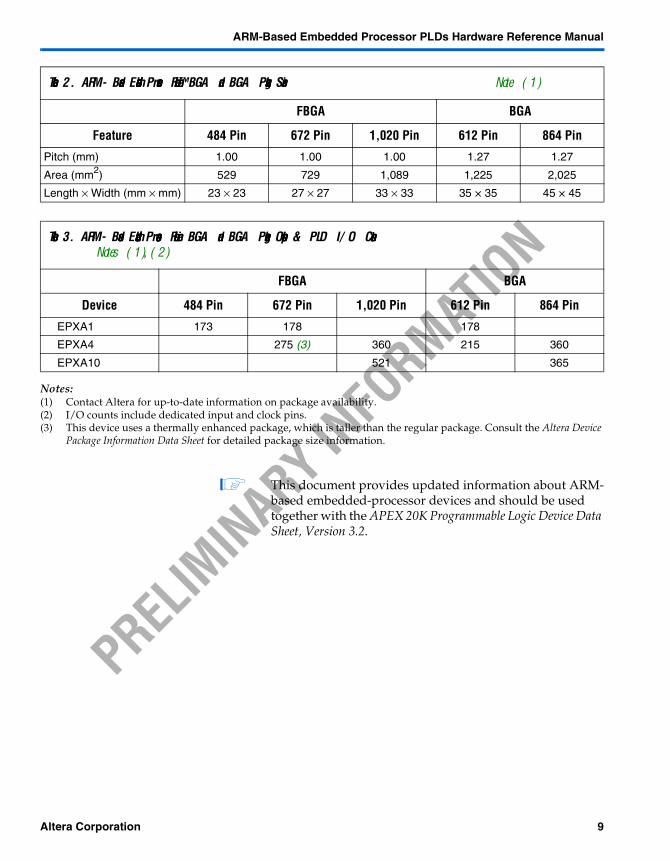
Notes:(1) Contact Altera for up-to-date information on package availability.(2) I/O counts include dedicated input and clock pins.(3) This device uses a thermally enhanced package, which is taller than the regular package. Consult the Altera Device
Package Information Data Sheet for detailed package size information.
This document provides updated information about ARM-based embedded-processor devices and should be used together with the APEX 20K Programmable Logic Device Data Sheet, Version 3.2.
Table 2. ARM-Based Embedded Processor FineLine™ BGA and BGA Package Sizes Note (1)
FBGA BGA
Feature 484 Pin 672 Pin 1,020 Pin 612 Pin 864 Pin
Pitch (mm) 1.00 1.00 1.00 1.27 1.27
Area (mm2) 529 729 1,089 1,225 2,025
Length × Width (mm × mm) 23 × 23 27 × 27 33 × 33 35 × 35 45 × 45
Table 3. ARM-Based Embedded Processor FineLine BGA and BGA Package Options & PLD I/O Counts Notes (1), (2)
FBGA BGA
Device 484 Pin 672 Pin 1,020 Pin 612 Pin 864 Pin
EPXA1 173 178 178
EPXA4 275 (3) 360 215 360
EPXA10 521 365
Altera Corporation 9
ARM-Based Embedded Processor PLDs Hardware Reference Manual
PRELIM
INARY IN
FORMAT
ION
General Description
Part of the Altera Excalibur embedded processor PLD solutions, the family of ARM®-based embedded-processor devices combines an unparalleled degree of integration and programmability. The ARM-based devices are outstanding embedded system development platforms, providing embedded-processor and PLD performance that is leading edge, yet cost efficient.
The ARM-based devices are offered in a variety of PLD device densities and memory sizes to fit a wide range of applications and requirements. Their high-performance, yet flexible, embedded architecture is ideal for compute-intensive and high data-bandwidth applications.
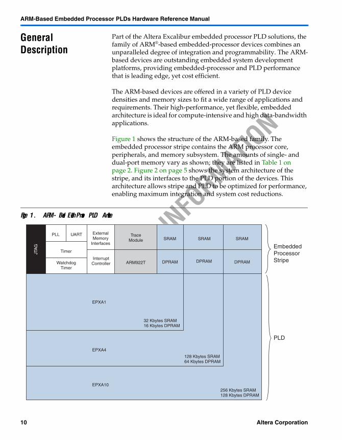
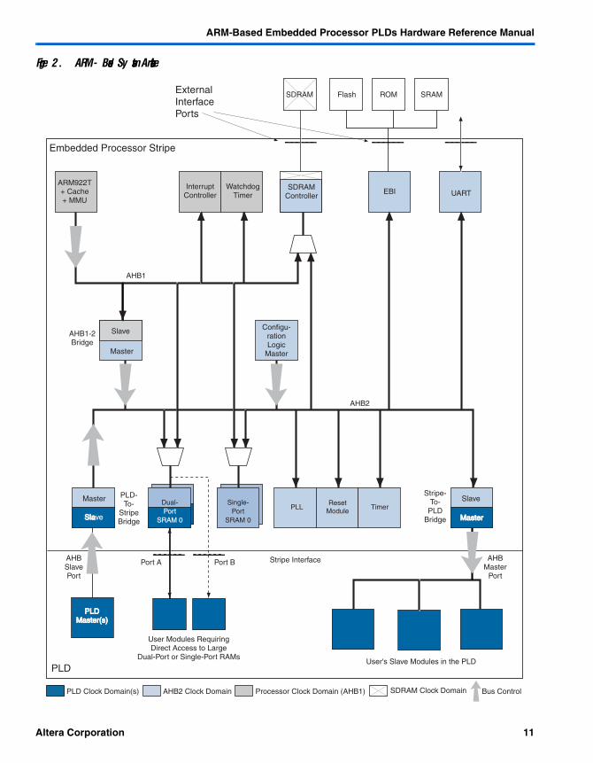
Figure 1 shows the structure of the ARM-based family. The embedded processor stripe contains the ARM processor core, peripherals, and memory subsystem. The amounts of single- and dual-port memory vary as shown; they are listed in Table 1 on page 2. Figure 2 on page 5 shows the system architecture of the stripe, and its interfaces to the PLD portion of the devices. This architecture allows stripe and PLD to be optimized for performance, enabling maximum integration and system cost reductions.
Figure 1. ARM-Based Embedded Processor PLD Architecture
PLL
Timer
UART
InterruptControllerWatchdog
Timer
JTA
G
128 Kbytes SRAM64 Kbytes DPRAM
32 Kbytes SRAM16 Kbytes DPRAM
256 Kbytes SRAM128 Kbytes DPRAM
EmbeddedProcessorStripe
PLD
DPRAM
EPXA1
EPXA4
EPXA10
TraceModule
ARM922T
SRAM SRAM SRAM
DPRAM DPRAM
ExternalMemory
Interfaces
10 Altera Corporation
ARM-Based Embedded Processor PLDs Hardware Reference Manual
PRELIM
INARY IN
FORMAT
ION
Figure 2. ARM-Based System Architecture
ARM922T+ Cache+ MMU
InterruptController
WatchdogTimer
SDRAMController
EBI UART
AHB1-2Bridge
Slave
Master
SlaveMaster
Configu-rationLogic
Master
Single-Port
SRAM 0
PLLReset
Module Timer
PLDPLDMaster(s)Master(s)
Port A Port B
User's Slave Modules in the PLD
Stripe Interface
AHB1
AHB2
Stripe-To-
PLDBridge
PLD-To-
StripeBridge
PLD
ExternalInterfacePorts
Embedded Processor Stripe
Flash ROM SRAM
SlaSlave
AHBMaster
Port
AHBSlavePort
User Modules RequiringDirect Access to Large
Dual-Port or Single-Port RAMs
PLD Clock Domain(s) AHB2 Clock Domain Processor Clock Domain (AHB1)
MasterMaster
Dual-Port
SRAM 0
Bus ControlSDRAM Clock Domain
SDRAM
Altera Corporation 11
ARM-Based Embedded Processor PLDs Hardware Reference Manual
PRELIM
INARY IN
FORMAT
ION
Two AMBA-compliant AHB buses ensure that ARM-based embedded processor activity is unaffected by peripheral and memory operation. Three bidirectional AHB bridges enable the peripherals and PLD to exchange data with the ARM-based embedded processor.
The performance of the ARM-based family is not compromised by the addition of interfaces to or from the stripe, and is equivalent to an ASIC implementation of an ARM922T on a 0.18-µm CMOS process. The ARMv4T instruction set is binary-compatible with many other ARM family members.
ARM-based embedded processor devices are supported by the Altera Quartus development system. Quartus is a single, integrated package that offers HDL and schematic design entry, compilation and logic synthesis, full simulation and worst-case timing analysis, SignalTap logic analysis, and device configuration. The Quartus software runs on Windows-based PCs, Sun SPARCstations, and HP 9000 Series 700/800 workstations.
The Quartus software provides NativeLink™ interfaces to other industry-standard PC- and UNIX workstation-based electronic-design automation (EDA) tools. For example, designers can invoke the Quartus software from within third-party design tools. Further, the Quartus software contains built-in optimized synthesis libraries; synthesis tools can use these libraries to optimize designs for ARM-based embedded processor devices.
Functional Description
The ARM-based embedded processor PLDs have a system architecture (embedded processor bus structure, on-chip memory, and peripherals) that combines the advantages of ASIC integration with PLD flexibility.
ARM-Based Embedded Processor
The ARM922T is a member of the ARM9 Thumb family of processor cores, with Harvard architecture implemented using a five-stage pipeline. This implementation allows single clock-cycle instruction operation through simultaneous fetch, decode, execute, memory, and write stages. It supports both the 32-bit ARM and 16-bit Thumb instruction sets, allowing users to achieve a balance between high code-density and performance.
12 Altera Corporation
ARM-Based Embedded Processor PLDs Hardware Reference Manual
PRELIM
INARY IN
FORMAT
ION
Independent of PLD configuration, the embedded processor can undertake the following activities:
Access external boot memory Boot and run Program/reprogram the PLD without corruption of memory Run interactive debugging Detect errors and restart/reboot/reprogram the entire system
as necessary Communicate with the external world and reconfigure the PLD Run a real-time operating system
PLD Interfaces
The PLD can be configured via the configuration interface or the embedded processor to implement various devices:
Additional peripherals that connect to the embedded bus as masters, slaves, or both
Coprocessors sharing the stripe as well as on-chip and off-chip memories
Standard interface to on-chip dual-port RAM (allowing SRAM to function as a ‘large’ embedded system block (ESB))
Additional embedded processor interrupt sources and controls
The master/slave/memory ports are synchronous to the separate PLD clock domains that drive them; however, the embedded processor domain and PLD domain can be asynchronous, to allow optimized clock frequencies for each domain. Resynchronization across the domains is handled by the AHB bridges within the stripe.
Both the master port and slave port of the stripe are capable of supporting 32-bit data accesses to the whole 4-Gbyte address range (32-bit address bus).
The PLD can take full advantage of the extensive range of Altera intellectual property (IP) Megacore® functions, reducing time-to-market and enabling complex SOPC designs.
PLLs
The device PLLs build on the PLL features of the APEX 20KE devices.
Altera Corporation 13
ARM-Based Embedded Processor PLDs Hardware Reference Manual
PRELIM
INARY IN
FORMAT
ION
Within the PLD, four PLLs are available, as in the APEX devices. In addition to the four APEX PLLs, ARM-based embedded processor PLDs have two ClockBoost PLLs that are frequency-programmable, both at configuration and via the system bus, to provide clocks for the following devices:
Embedded processor and associated modules Memory controller
The additional PLLs and associated routing support the following features:
A common source for running additional PLLs Clock generation for the embedded processor and memory
subsystem, allowing a synchronous mode LVTTL 2.5-V and 3.3-V clock input PLL disabling, which allows the raw input clock to be routed as
the main clock source
The memory controller PLL allows users to tune the frequency of the system clock to the speed of the external memory implemented in their systems.
External Memory Controllers
The ARM-based embedded processor PLDs provide two embedded memory controllers that can be accessed by any of the bus masters: one for external DRAM, and a second for external flash memory or SRAM.
The DRAM memory controller supports the following commonly-available memory standards, without the addition of any glue logic:
Single-data rate (SDR) 133-MHz data rates Double-data rate (DDR) 266-MHz data rates
A software-programmable PLL is used within the DRAM memory controller subsystem to supply the appropriate timings. Users can program the frequency to match the chosen memory components.
A second memory controller supports the interface to system ROM, allowing external flash memory access and reprogramming. In addition, static RAM and simple peripherals can be connected to this interface externally.
14 Altera Corporation
ARM-Based Embedded Processor PLDs Hardware Reference Manual
PRELIM
INARY IN
FORMAT
ION
Peripherals
The following peripherals are connected to the AHB:
UART Timer Watchdog timer Interrupt controller
Registers All registers are located within one 16-Kbyte memory region, which is located at address 7FFFC000H at reset. This memory region can be relocated at any time. Offsets in this section are from its base address.
At reset, all registers hold the value 0 unless otherwise specified.
Table 4 shows the effect of a read or a write to the embedded-logic registers:
See the section “Embedded Processor Register Summary” on page 159 for a comprehensive list of all registers apart from the memory map control registers, which are detailed below.
Memory Map The devices listed in Table 5 are present as slaves in the memory map:
Table 4. Effects of Accessing Registers
R Read access (no side effects)
R* Read access with possible side effects (such as clearing some of the bits or clearing an interrupt)
W Writes of 1 or 0 set writable bits to the values specified
S Writes of 1 set bits. Writes of 0 do nothing.
C Writes of 1 clear the appropriate bits. Writes of 0 do nothing.
Table 5. Memory Map Devices
Memory Range Size (bytes)
EBI0, EBI1, EBI2, EBI3 16 Kbytes to 32 Mbytes each
SDRAM0, SDRAM1 16 Kbytes to 256 Mbytes each
Internal SRAM0, SRAM1 256 Kbytes total (for EPXA10)
Internal dual-port DPSRAM0, DPSRAM1 128 Kbytes total (for EPXA10)
Registers 16 Kbytes
PLD ranges PLD0, PLD1, PLD2, PLD3 16 Kbytes to 2 Gbytes each
Altera Corporation 15
ARM-Based Embedded Processor PLDs Hardware Reference Manual
PRELIM
INARY IN
FORMAT
ION
A memory range can be set to any size that is a power of two.
Ensure that memory ranges do not overlap. If an address decodes into more than one range, the results are undefined (ranges may temporarily overlap during reconfiguration, providing that no accesses are made to that range).
Memory Mapping in Boot-From-Flash Mode
An additional mapping (the boot memory mapping) can be present at address 0H in boot-from-flash mode. This mapping is the first 32 Kbytes of EBI0. It is enabled after reset and can be disabled using the boot-configuration register, BOOT_CR (see page 104).
Memory Map Control Registers
The memory map control registers are accessed from AHB2, which means that they can be accessed by the embedded processor, by the configuration logic, or via the PLD-to-stripe bridge.
Only word accesses to the memory map control registers are allowed; half word or byte accesses generate a bus error.
To ensure that any changes have taken effect, the user must either disable write-posting in the bridge or follow each write with a safe-read instruction that will pass through the AHB1-2 bridge. The new address map does not take effect until any posted write outstanding on AHB2 has completed.
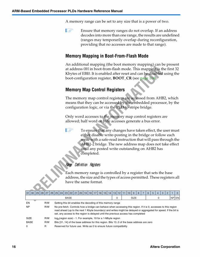
Range Definition Registers
Each memory range is controlled by a register that sets the base address, the size and the types of access permitted. These registers all have the same format.
EN R/W Setting this bit enables the decoding of this memory range
NP R/W No pre-fetch. Controls how a bridge can behave when accessing this region. If it is 0, accesses to this region read ahead (up to the next 1 Kbyte boundary) and writes might be delayed or aggregated for speed. If the bit is set, any access to the region is delayed until the previous access has completed
SIZE R/W log2(region size) - 1. For example, 19 for a 1-Mbyte region
BASE R/W Bits [31..14] of the base address for this region. Bits 13..0 of the base address are zero
0 R Reserved for future use. Write as 0 to ensure future compatibility
12345678910111213141516171819202122232425262728293031 0
BASE 0 SIZE 0 NP EN
16 Altera Corporation
ARM-Based Embedded Processor PLDs Hardware Reference Manual
PRELIM
INARY IN
FORMAT
ION
If SIZE is set to a value less than 13, the address decoding logic assumes 13. This corresponds to a minimum size of 16 Kbytes for each enabled region.
Setting BASE to a value that is not a multiple of the region size or a multiple of the underlying size produces undefined results.
Most of the range definition registers are fully read/write enabled. For some registers, the SIZE and NP bits are read-only. Table 6 lists their values.
Register: MMAP_REGISTERSAddress: Register base + 80HAccess: Read/write
At reset, the read/write bits in all range registers are set to zero, except for the registers’ base address, which is enabled at address 7FFFC000H. The size of the registers region is fixed at 16 Kbytes.
Clearing the register-enable bit, RE, in register BOOT_CR (see page 104), or the enable bit, EN, in register MMAP_REGISTERS disables the registers region. The device must be reset to re-enable it.
Register: MMAP_SRAM0 (on-chip SRAM block 0)Address: Register base + 90HAccess: Read/write
Register: MMAP_SRAM1 (on-chip SRAM block 1)Address: Register base + 94HAccess: Read/write
Register: MMAP_DPSRAM0 (dual-port SRAM block 0)Address: Register base + A0HAccess: Read/write
Table 6. SIZE and NP Fields in the Range Definition Registers
Range Definition Register Size NP
MMAP_EBI0, MMAP_EBI1, MMAP_EBI2, MMAP_EBI3 - -
MMAP_SDRAM0, MMAP_SDRAM1 - 0
MMAP_SRAM0, MMAP_SRAM1 (internal SRAM) - 0
MMAP_DPSRAM0, MMAP_DPSRAM1 (internal dual-port RAM) - 0
MMAP_REGISTERS 13 1
MMAP_PLD0, MMAP_PLD1, MMAP_PLD2, MMAP_PLD3 (PLD ranges) - -
Altera Corporation 17
ARM-Based Embedded Processor PLDs Hardware Reference Manual
PRELIM
INARY IN
FORMAT
ION
Register: MMAP_DPSRAM1 (dual-port SRAM block 1)Address: Register base + A4HAccess: Read/write
Register: MMAP_SDRAM0 (SDRAM block 0)Address: Register base + B0HAccess: Read/write
Register: MMAP_SDRAM1 (SDRAM block 1)Address: Register base + B4HAccess: Read/write
Register: MMAP_EBI0 (EBI block 0)Address: Register base + C0HAccess: Read/write
Register: MMAP_EBI1 (EBI block 1)Address: Register base + C4HAccess: Read/write
Register: MMAP_EBI2 (EBI block 2)Address: Register base + C8HAccess: Read/write
Register: MMAP_EBI3 (EBI block 3)Address: Register base + CCHAccess: Read/write
Register: MMAP_PLD0 (PLD region 0)Address: Register base + D0HAccess: Read/write
Register: MMAP_PLD1 (PLD region 1)Address: Register base + D4HAccess: Read/write
Register: MMAP_PLD2 (PLD region 2)Address: Register base + D8HAccess: Read/write
Register: MMAP_PLD3Address: Register base + DCH (PLD region 3)Access: Read/write
Four memory ranges are provided, which select the PLD bridge. The select signals for these four regions are combined in the bridge and are not made available separately to the PLD.
18 Altera Corporation
ARM-Based Embedded Processor PLDs Hardware Reference Manual
PRELIM
INARY IN
FORMAT
ION
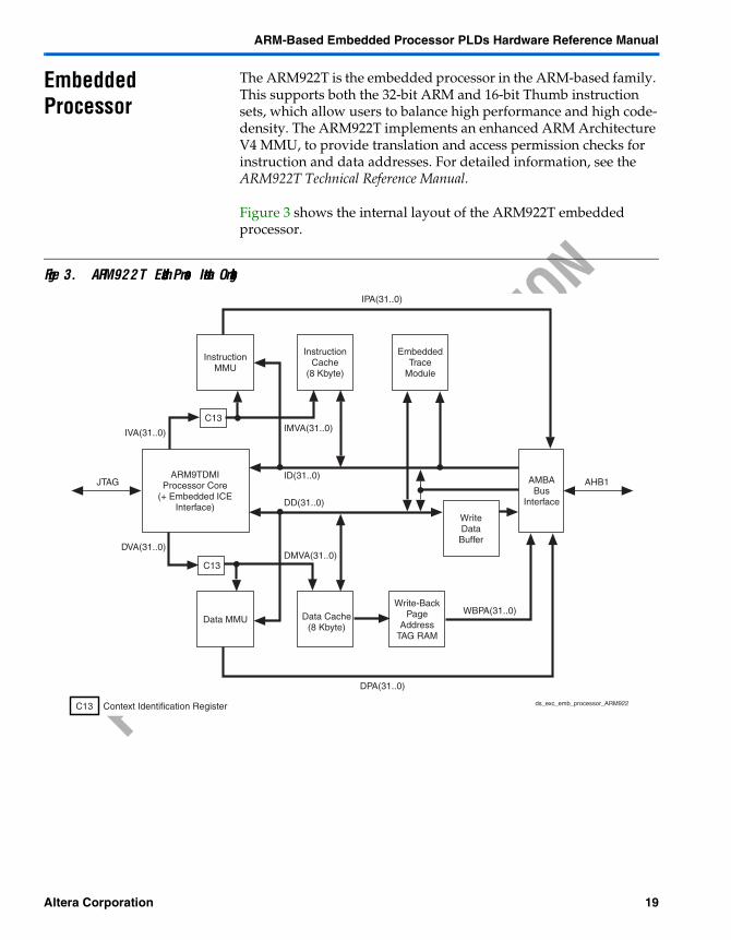
Embedded Processor
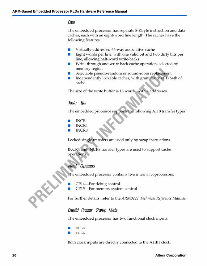
The ARM922T is the embedded processor in the ARM-based family. This supports both the 32-bit ARM and 16-bit Thumb instruction sets, which allow users to balance high performance and high code-density. The ARM922T implements an enhanced ARM Architecture V4 MMU, to provide translation and access permission checks for instruction and data addresses. For detailed information, see the ARM922T Technical Reference Manual.
Figure 3 shows the internal layout of the ARM922T embedded processor.
Figure 3. ARM922T Embedded Processor Internal Organization
AMBABus
Interface
EmbeddedTrace
Module
WriteDataBuffer
Write-BackPage
AddressTAG RAM
InstructionMMU
InstructionCache
(8 Kbyte)
ARM9TDMIProcessor Core
(+ Embedded ICEInterface)
Data MMU Data Cache(8 Kbyte)
AHB1JTAG
C13
C13
IVA(31..0)
IPA(31..0)
DPA(31..0)
WBPA(31..0)
DVA(31..0)
IMVA(31..0)
DMVA(31..0)
ID(31..0)
DD(31..0)
C13 Context Identification Register ds_exc_emb_processor_ARM922
Altera Corporation 19
ARM-Based Embedded Processor PLDs Hardware Reference Manual
PRELIM
INARY IN
FORMAT
ION
Cache
The embedded processor has separate 8-Kbyte instruction and data caches, each with an eight-word line length. The caches have the following features:
Virtually-addressed 64-way associative cache Eight words per line, with one valid bit and two dirty bits per
line, allowing half-word write-backs Write-through and write-back cache operation, selected by
memory region Selectable pseudo-random or round-robin replacement Independently lockable caches, with granularity of 1/64th of
cache
The size of the write buffer is 16 words, with 4 addresses.
Transfer Types
The embedded processor supports the following AHB transfer types:
INCR INCR4 INCR8
Locked single transfers are used only by swap instructions.
INCR4 and INCR8 transfer types are used to support cache operations.
Internal Coprocessors
The embedded processor contains two internal coprocessors:
CP14—For debug control CP15—For memory system control
For further details, refer to the ARM922T Technical Reference Manual.
Embedded Processor Clocking Modes
The embedded processor has two functional clock inputs:
BCLK FCLK
Both clock inputs are directly connected to the AHB1 clock.
20 Altera Corporation
ARM-Based Embedded Processor PLDs Hardware Reference Manual
PRELIM
INARY IN
FORMAT
ION
There are three clocking modes for ARM-based embedded processor devices:
Fast bus Synchronous Asynchronous
The ARM-based devices, by default, use fast bus mode, which is the recommended mode.
For further details about clocking modes and the embedded processor clock inputs, see the ARM922T Technical Reference Manual.
Endianness
The endianness of the stripe is set by writing to the coprocessor registers; see the ARM922T Technical Reference Manual for details.
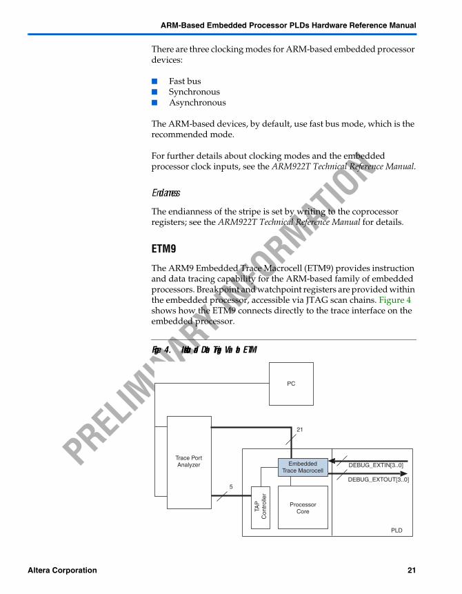
ETM9
The ARM9 Embedded Trace Macrocell (ETM9) provides instruction and data tracing capability for the ARM-based family of embedded processors. Breakpoint and watchpoint registers are provided within the embedded processor, accessible via JTAG scan chains. Figure 4 shows how the ETM9 connects directly to the trace interface on the embedded processor.
Figure 4. Instruction and Data Tracing Via the ETM
PC
Trace PortAnalyzer
TAP
Con
trol
ler
ProcessorCore
5
21
DEBUG_EXTIN[3..0]
DEBUG_EXTOUT[3..0]
EmbeddedTrace Macrocell
PLD
Altera Corporation 21
ARM-Based Embedded Processor PLDs Hardware Reference Manual
PRELIM
INARY IN
FORMAT
ION
Debug Communications Channel
Coprocessor CP14 in the embedded processor contains a communications unit, which allows software on the embedded processor to communicate with a debugger via JTAG. COMMRX and COMMTX are routed from CP14 to the interrupt controller and the PLD as INT_COMMRX and INT_COMMTX respectively.
Port Size and ETM Port Selection
PORTSIZE and ETMEN settings control the width of the output port, which reduces the number of pins that need to be dedicated to the TRACE_PKT bus. The maximum size of the trace port is 16 bits. See the ARM9 Embedded Trace Macrocell Technical Reference Manual for further information.
At reset, the ETM9 is disabled and a 4-bit port is selected. When the debug session starts, the debug tools control ETMEN and PORTSIZE by programming the ETM control register.
External Inputs
The four inputs on the DEBUG_EXTIN[3..0] bus are routed from the PLD and provide coarse enable/disable tracing control for the trigger or enable signals. Signals are synchronized to the ETM9 clock by two registers.
External Outputs
Four outputs on the DEBUG_EXTOUT[3..0] bus are routed to the PLD. Each is controlled by an ETM9 event, which can be programmed in the usual way.
22 Altera Corporation
ARM-Based Embedded Processor PLDs Hardware Reference Manual
PRELIM
INARY IN
FORMAT
ION
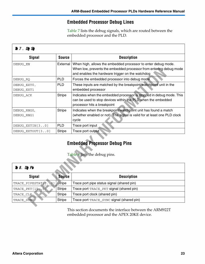
Embedded Processor Debug Lines
Table 7 lists the debug signals, which are routed between the embedded processor and the PLD.
Embedded Processor Debug Pins
Table 8 lists the debug pins.
This section documents the interface between the ARM922T embedded processor and the APEX 20KE device.
Table 7. Debug Signals
Signal Source Description
DEBUG_EN External When high, allows the embedded processor to enter debug mode.When low, prevents the embedded processor from entering debug mode and enables the hardware trigger on the watchdog
DEBUG_RQ PLD Forces the embedded processor into debug mode
DEBUG_EXT0, DEBUG_EXT1
PLD These inputs are matched by the breakpoint/watchpoint unit in the embedded processor
DEBUG_ACK Stripe Indicates when the embedded processor is stopped in debug mode. This can be used to stop devices within the PLD when the embedded processor hits a breakpoint
DEBUG_RNG0,DEBUG_RNG1
Stripe Indicates when the breakpoint/watchpoint unit has found a match (whether enabled or not). The signal is valid for at least one PLD clock cycle
DEBUG_EXTIN[3..0] PLD Trace port input
DEBUG_EXTOUT[3..0] Stripe Trace port output
Table 8. Debug Pins
Signal Source Description
TRACE_PIPESTAT[2..0] Stripe Trace port pipe status signal (shared pin)
TRACE_PKT[15..0] Stripe Trace port TRACE_PKT signal (shared pin)
TRACE_CLK Stripe Trace port clock (shared pin)
TRACE_SYNC Stripe Trace port TRACE_SYNC signal (shared pin)
Altera Corporation 23
ARM-Based Embedded Processor PLDs Hardware Reference Manual
PRELIM
INARY IN
FORMAT
ION
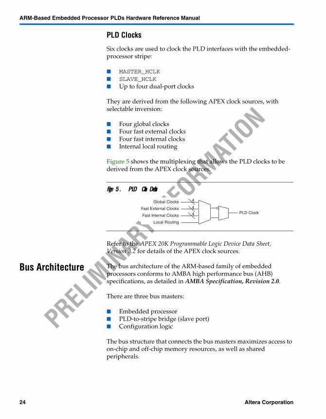
PLD Clocks
Six clocks are used to clock the PLD interfaces with the embedded-processor stripe:
MASTER_HCLK SLAVE_HCLK Up to four dual-port clocks
They are derived from the following APEX clock sources, with selectable inversion:
Four global clocks Four fast external clocks Four fast internal clocks Internal local routing
Figure 5 shows the multiplexing that allows the PLD clocks to be derived from the APEX clock sources.
Figure 5. PLD Clock Derivation
Refer to the APEX 20K Programmable Logic Device Data Sheet, Version 3.2 for details of the APEX clock sources.
Bus Architecture The bus architecture of the ARM-based family of embedded processors conforms to AMBA high performance bus (AHB) specifications, as detailed in AMBA Specification, Revision 2.0.
There are three bus masters:
Embedded processor PLD-to-stripe bridge (slave port) Configuration logic
The bus structure that connects the bus masters maximizes access to on-chip and off-chip memory resources, as well as shared peripherals.
Global Clocks
Fast External Clocks
Fast Internal Clocks
Local Routing
PLD Clock
4
4
4
24 Altera Corporation
ARM-Based Embedded Processor PLDs Hardware Reference Manual
PRELIM
INARY IN
FORMAT
ION
The embedded processor master has a dedicated 32-bit bus (AHB1). The remaining bus masters (PLD-to-stripe bridge and configuration logic) share the AHB2 bus with the AHB1-2 bridge, to access the remaining slave modules. Both AHB1 and AHB2 support locked transfers.
By providing address and control information, bus masters can initiate read and write operations using 32-bit read and write data buses and a 32-bit address bus. However, bus use is controlled by the bus arbiter, which allows only one bus master at a time to initiate bus transfers. Bus slaves respond to read and write operations within a given address-space range, signaling to the active master whether the bus transfer was a success, failure, or is still waiting.
The AHB1 and AHB2 masters can access different blocks of on-chip SRAM concurrently, because each bus has its own arbitration.
Any bus master implemented in the PLD can access slave modules implemented in the PLD via AHB2.
The AHB standard is used for the stripe and also for the master and slave interfaces between the stripe and the PLD. However, when the dual-port memories are configured as on-chip SRAM for a PLD application, the AHB standard does not apply to the interface. See the section “On-Chip SRAM” on page 86 for details of this.
All AMBA AHB protocols are supported, including the following:
Incremental bursts of 4, 8, 16 and unspecified length Wrapping bursts of 4, 8 and16 length Early burst termination SPLIT response on AHB2 (EBI only) Locked transfers
Figure 6 on page 20 shows typical AHB transaction waveforms.
Altera Corporation 25
ARM-Based Embedded Processor PLDs Hardware Reference Manual
PRELIM
INARY IN
FORMAT
ION
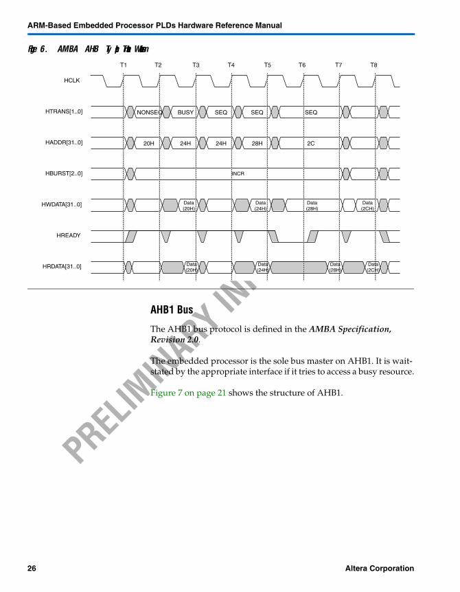
Figure 6. AMBA AHB Typical Transaction Waveforms
AHB1 Bus
The AHB1 bus protocol is defined in the AMBA Specification, Revision 2.0.
The embedded processor is the sole bus master on AHB1. It is wait-stated by the appropriate interface if it tries to access a busy resource.
Figure 7 on page 21 shows the structure of AHB1.
HCLK
HTRANS[1..0]
HADDR[31..0]
HBURST[2..0]
HWDATA[31..0]
HREADY
HRDATA[31..0]
NONSEQ BUSY SEQ SEQ SEQ
20H 24H 24H 28H 2C
INCR
Data(20H)
Data(24H)
Data(28H)
Data(2CH)
Data(20H)
Data(24H)
Data(28H)
Data(2CH)
T1 T2 T3 T4 T5 T6 T7 T8
26 Altera Corporation
ARM-Based Embedded Processor PLDs Hardware Reference Manual
PRELIM
INARY IN
FORMAT
ION
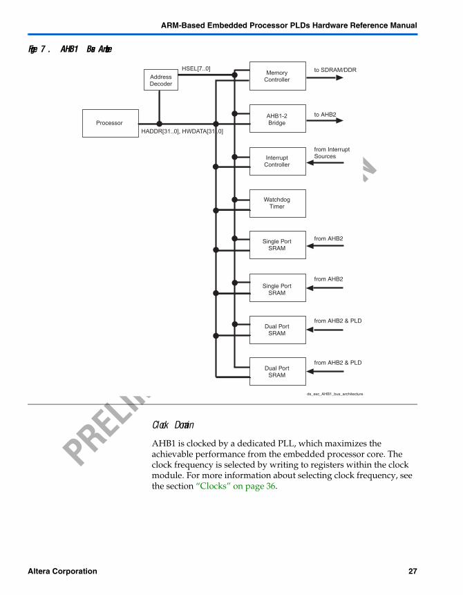
Figure 7. AHB1 Bus Architecture
Clock Domain
AHB1 is clocked by a dedicated PLL, which maximizes the achievable performance from the embedded processor core. The clock frequency is selected by writing to registers within the clock module. For more information about selecting clock frequency, see the section “Clocks” on page 36.
AddressDecoder
HADDR[31..0], HWDATA[31..0]
HSEL[7..0]Memory
Controller
AHB1-2Bridge
to SDRAM/DDR
to AHB2
InterruptController
from InterruptSources
WatchdogTimer
Single PortSRAM
from AHB2
Single PortSRAM
from AHB2
Dual PortSRAM
Dual PortSRAM
from AHB2 & PLD
from AHB2 & PLD
Processor
ds_exc_AHB1_bus_architecture
Altera Corporation 27
ARM-Based Embedded Processor PLDs Hardware Reference Manual
PRELIM
INARY IN
FORMAT
ION
Address Decoder
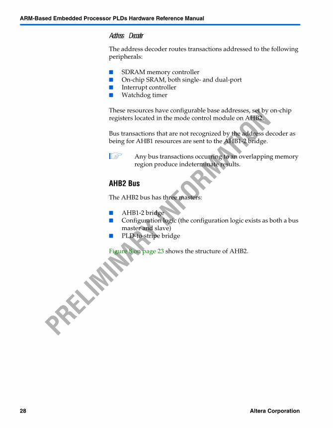
The address decoder routes transactions addressed to the following peripherals:
SDRAM memory controller On-chip SRAM, both single- and dual-port Interrupt controller Watchdog timer
These resources have configurable base addresses, set by on-chip registers located in the mode control module on AHB2.
Bus transactions that are not recognized by the address decoder as being for AHB1 resources are sent to the AHB1-2 bridge.
Any bus transactions occurring to an overlapping memory region produce indeterminate results.
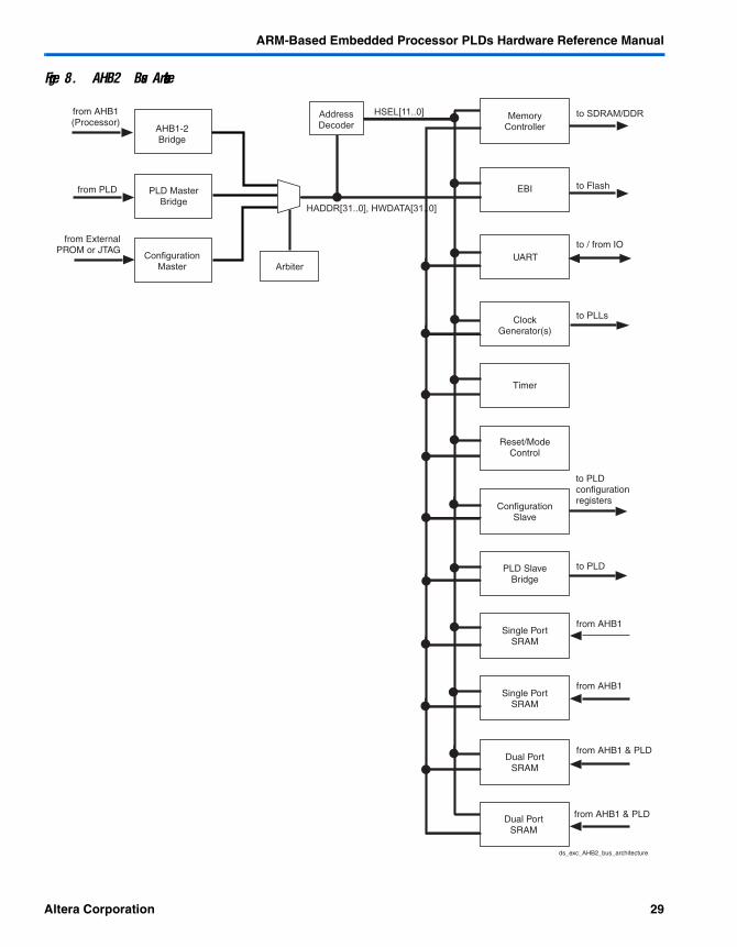
AHB2 Bus
The AHB2 bus has three masters:
AHB1-2 bridge Configuration logic (the configuration logic exists as both a bus
master and slave) PLD-to-stripe bridge
Figure 8 on page 23 shows the structure of AHB2.
28 Altera Corporation
ARM-Based Embedded Processor PLDs Hardware Reference Manual
PRELIM
INARY IN
FORMAT
ION
Figure 8. AHB2 Bus Architecture
from ExternalPROM or JTAG
from PLD
from AHB1(Processor)
AHB1-2Bridge
PLD MasterBridge
ConfigurationMaster Arbiter
AddressDecoder
HSEL[11..0] MemoryController
EBI
to SDRAM/DDR
to Flash
UARTto / from IO
ClockGenerator(s)
to PLLs
Timer
Reset/ModeControl
ConfigurationSlave
to PLDconfigurationregisters
PLD SlaveBridge
to PLD
Single PortSRAM
from AHB1
Single PortSRAM
from AHB1
Dual PortSRAM
Dual PortSRAM
from AHB1 & PLD
from AHB1 & PLD
HADDR[31..0], HWDATA[31..0]
ds_exc_AHB2_bus_architecture
Altera Corporation 29
ARM-Based Embedded Processor PLDs Hardware Reference Manual
PRELIM
INARY IN
FORMAT
ION
The AHB2 arbiter controls access to the bus.
AHB2 Arbiter
The AHB2 arbiter determines which requesting master should have priority access when there is contention for the bus during busy periods.
When the bus is not busy, the arbiter parks the bus on the PLD-to-stripe bridge.
Split Transactions
The arbiter supports split transactions, but only from the EBI. Split transactions allow other masters to access the buses while a high-latency slave access, such as reading flash memory, is in progress. They are a means of improving the system performance of slow peripherals.
If a transfer is likely to take a large number of cycles to perform, the EBI can issue a split response. On receiving a split response, the arbiter de-asserts the bus grant to the requesting master, and masks further requests from that master until the EBI removes the split. This denies that master any access to the bus until the EBI is ready to complete the transfer, although other masters are free to use the bus.
Clock Domain
AHB2 is clocked by the AHB1 clock divided down by 2. The frequency is selected by writing to a register in the clock module. For more information about selecting clock frequency, see the section “Clocks” on page 36.
Locked Transfers
AHB2 allows locked transfers. Masters request locked access to memory by asserting MASTER_HLOCK at the same time as MASTER_HBUSREQ. In this situation, the bus remains granted to the master until MASTER_HLOCK is de-asserted.
30 Altera Corporation
ARM-Based Embedded Processor PLDs Hardware Reference Manual
PRELIM
INARY IN
FORMAT
ION
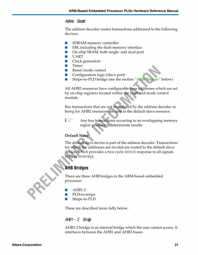
Address Decoder
The address decoder routes transactions addressed to the following devices:
SDRAM memory controller EBI, including the flash memory interface On-chip SRAM, both single- and dual-port UART Clock generators Timer Reset/mode control Configuration logic (slave port) Stripe-to-PLD bridge (see the section ”AHB Bridges” below)
All AHB2 resources have configurable base addresses which are set by on-chip registers located within the reset and mode control module.
Bus transactions that are not recognized by the address decoder as being for AHB2 resources are sent to the default slave resource.
Any bus transactions occurring to an overlapping memory region produce indeterminate results.
Default Slave
The default slave device is part of the address decoder. Transactions for which the addresses are invalid are routed to the default slave device, which provides a two-cycle ERROR response to all signals (SEQ or NONSEQ).
AHB Bridges
There are three AHB bridges in the ARM-based embedded processor:
AHB1-2 PLD-to-stripe Stripe-to-PLD
These are described more fully below.
AHB1-2 Bridge
AHB1-2 bridge is an internal bridge which the user cannot access. It interfaces between the AHB1 and AHB2 buses.
Altera Corporation 31
ARM-Based Embedded Processor PLDs Hardware Reference Manual
PRELIM
INARY IN
FORMAT
ION
There is no need for synchronization logic in the AHB1-2 bridge, because AHB1 and AHB2 always operate synchronously to each other.
PLD-to-Stripe and Stripe-to-PLD Bridges
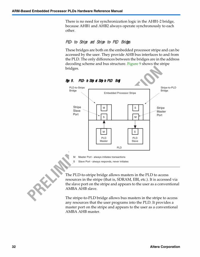
These bridges are both on the embedded processor stripe and can be accessed by the user. They provide AHB bus interfaces to and from the PLD. The only differences between the bridges are in the address decoding scheme and bus structure. Figure 9 shows the stripe bridges.
Figure 9. PLD-to-Stripe and Stripe-to-PLD Bridges
The PLD-to-stripe bridge allows masters in the PLD to access resources in the stripe (that is, SDRAM, EBI, etc.). It is accessed via the slave port on the stripe and appears to the user as a conventional AMBA AHB slave.
The stripe-to-PLD bridge allows bus masters in the stripe to access any resources that the user programs into the PLD. It provides a master port on the stripe and appears to the user as a conventional AMBA AHB master.
M S
S M
M Master Port - always initiates transactions
Slave Port - always responds, never initiatesS
M S
Embedded Processor Stripe
PLD
StripeMasterPort
StripeSlavePort
PLD-to-StripeBridge
Stripe-to-PLDBridge
PLDMaster
PLDSlave
32 Altera Corporation
ARM-Based Embedded Processor PLDs Hardware Reference Manual
PRELIM
INARY IN
FORMAT
ION
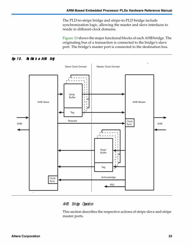
The PLD-to-stripe bridge and stripe-to-PLD bridge include synchronization logic, allowing the master and slave interfaces to reside in different clock domains.
Figure 10 shows the major functional blocks of each AHB bridge. The originating bus of a transaction is connected to the bridge’s slave port. The bridge’s master port is connected to the destination bus.
Figure 10. Functional Blocks of an AHB Bridge
AHB Bridge Operation
This section describes the respective actions of stripe slave and stripe master ports.
AHB Slave
AHB
WriteBuffer
Tag
ReadBuffer
Tag
AHB Master
AHBRequest
ClockSync
Acknowledge
IRQ
ClockSync
Slave Clock Domain Master Clock Domain
Altera Corporation 33
ARM-Based Embedded Processor PLDs Hardware Reference Manual
PRELIM
INARY IN
FORMAT
ION
Slave Interface
Write requests from the AHB slave interface are synchronized to the master clock domain. The write buffer accepts bursts of posted-write data while buffer entries are free to accept data, otherwise it inserts wait states. The AHB master interface takes data from the buffer and writes it to the destination bus, asserting an acknowledge to indicate that a buffer entry is now free for reuse by the slave.
In non-posted mode, write buffer tags are used to return the status of the master write (OK, ERROR, RETRY and so on). Each write buffer entry has one write-request, one write-acknowledge, and one write tag.
When selected by a read transaction, the AHB slave asserts a read request, which must be synchronized to the master clock domain. Address and control information is passed to the master interface, but is not placed in the buffer. The AHB master performs a read transaction (pre-fetching data to fill the buffer, if enabled) and asserts an acknowledge to indicate when data is available. If, during a read transaction, no data is available from the read buffer, the slave interface inserts wait states. Read buffer tags are used to return the status of the transaction (OK, ERROR, RETRY and so on). Each read buffer entry has one read-request, one read-acknowledge and one read tag.
If a posted-write transaction had an ERROR response, an interrupt is generated. Diagnostic details can be obtained via the appropriate bridge status register.
Master Interface
When the slave interface indicates that a transfer is pending, the master interface uses the address and control information to perform the requested transaction on the destination bus.
The master reads data from the destination bus only if there is a free entry in the read buffer to receive it. If no free entries are available, the master interface inserts BUSY cycles. Similarly, if no data is available from the write buffer during a write transaction, the master interface inserts BUSY cycles.
If it loses access to the bus during a transaction, the master interface re-asserts its bus request and completes the transaction with an undefined-length transfer.
Byte and half-word accesses are allowed, with the master interface passing the transfer size to the slave interface unmodified.
34 Altera Corporation
ARM-Based Embedded Processor PLDs Hardware Reference Manual
PRELIM
INARY IN
FORMAT
ION
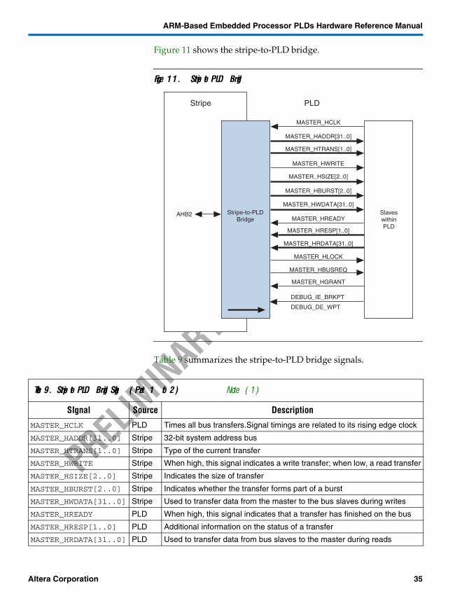
Figure 11 shows the stripe-to-PLD bridge.
Figure 11. Stripe-to-PLD Bridge
Table 9 summarizes the stripe-to-PLD bridge signals.
MASTER_HCLK
MASTER_HADDR[31..0]
MASTER_HTRANS[1..0]
MASTER_HWRITE
MASTER_HSIZE[2..0]
MASTER_HBURST[2..0]
MASTER_HWDATA[31..0]
MASTER_HREADY
MASTER_HRESP[1..0]
MASTER_HRDATA[31..0]
MASTER_HLOCK
MASTER_HBUSREQ
MASTER_HGRANT
Stripe-to-PLDBridge
SlaveswithinPLD
AHB2
Stripe PLD
DEBUG_IE_BRKPT
DEBUG_DE_WPT
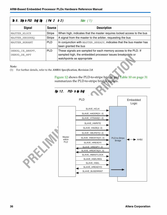
Table 9. Stripe-to-PLD Bridge Signals (Part 1 of 2) Note (1)
SIgnal Source Description
MASTER_HCLK PLD Times all bus transfers.Signal timings are related to its rising edge clock
MASTER_HADDR[31..0] Stripe 32-bit system address bus
MASTER_HTRANS[1..0] Stripe Type of the current transfer
MASTER_HWRITE Stripe When high, this signal indicates a write transfer; when low, a read transfer
MASTER_HSIZE[2..0] Stripe Indicates the size of transfer
MASTER_HBURST[2..0] Stripe Indicates whether the transfer forms part of a burst
MASTER_HWDATA[31..0] Stripe Used to transfer data from the master to the bus slaves during writes
MASTER_HREADY PLD When high, this signal indicates that a transfer has finished on the bus
MASTER_HRESP[1..0] PLD Additional information on the status of a transfer
MASTER_HRDATA[31..0] PLD Used to transfer data from bus slaves to the master during reads
Altera Corporation 35
ARM-Based Embedded Processor PLDs Hardware Reference Manual
PRELIM
INARY IN
FORMAT
IONNote:
(1) For further details, refer to the AMBA Specification, Revision 2.0.
Figure 12 shows the PLD-to-stripe bridge and Table 10 on page 31 summarizes the PLD-to-stripe bridge signals.
Figure 12. PLD-to-stripe Bridge.
MASTER_HLOCK Stripe When high, indicates that the master requires locked access to the bus
MASTER_HBUSREQ Stripe A signal from the master to the arbiter, requesting the bus
MASTER_HGRANT PLD In conjunction with MASTER_HREADY, indicates that the bus master has been granted the bus
DEBUG_IE_BRKPT, DEBUG_DE_WPT
PLD These signals are sampled for each memory access to the PLD. If sampled high, the embedded processor issues breakpoints or watchpoints as appropriate
Table 9. Stripe-to-PLD Bridge Signals (Part 2 of 2) Note (1)
SIgnal Source Description
SLAVE_HCLK
SLAVE_HADDR[31..0]
SLAVE_HTRANS[1..0]
SLAVE_HWRITE
SLAVE_HSIZE[2..0]
SLAVE_HBURST[2..0]
SLAVE_HWDATA[31..0]
SLAVE_HREADYI
SLAVE_HRESP[1..0]
SLAVE_HRDATA[31..0]
SLAVE_HMASTLOCK
SLAVE_HSELREG
SLAVE_HSEL
PLD-to-StripeBridge
MasterwithinPLD
AHB2
EmbeddedLogic
PLD
SLAVE_HREADYO
SLAVE_BUSERRINT
36 Altera Corporation
ARM-Based Embedded Processor PLDs Hardware Reference Manual
PRELIM
INARY IN
FORMAT
ION
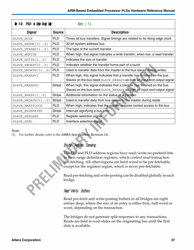
Note:(1) For further details, refer to the AMBA Specification, Revision 2.0.
Bridge Address Decoding
The EBI and PLD address regions have read/write no-prefetch bits in their range definition registers, which control read transaction pre-fetching. All other regions are hard wired to be pre-fetchable, except for the registers region, which is never pre-fetchable.
Read pre-fetching and write-posting can be disabled globally in each bridge.
Read/Write Buffers
Read pre-fetch and write-posting buffers in all bridges are eight entries deep, where the size of an entry is either byte, half-word or word, depending on the transaction.
The bridges do not generate split responses to any transactions. Reads are held in wait-states on the originating bus until the first data is available.
Table 10. PLD-to-Stripe Bridge Signals Note (1)
SIgnal Source Description
SLAVE_HCLK PLD Times all bus transfers. Signal timings are related to its rising edge clock
SLAVE_HADDR[31..0] PLD 32-bit system address bus
SLAVE_HTRANS[1..0] PLD The type of the current transfer
SLAVE_HWRITE PLD When high, this signal indicates a write transfer; when low, a read transfer
SLAVE_HSIZE[2..0] PLD Indicates the size of transfer
SLAVE_HBURST[2..0] PLD Indicates whether the transfer forms part of a burst
SLAVE_HWDATA[31..0] PLD Used to transfer data from the master to the bus slaves during writes
SLAVE_HREADYI PLD When high, this signal indicates that a transfer has finished on the bus. Slaves on the bus need SLAVE_HREADY as both an input and output signal
SLAVE_HREADYO Stripe When high, this signal indicates that a transfer has finished on the bus. Slaves on the bus need SLAVE_HREADY as both an input and output signal
SLAVE_HRESP[1..0] Stripe Additional information on the status of a transfer
SLAVE_HRDATA[31..0] Stripe Used to transfer data from bus slaves to the master during reads
SLAVE_HMASTLOCK PLD When high, indicates that the master requires locked access to the bus
SLAVE_BUSERRINT Stripe Interrupt signifying a bus error
SLAVE_HSELREG PLD Register selection signal
SLAVE_HSEL PLD Interface selection signal
Altera Corporation 37
ARM-Based Embedded Processor PLDs Hardware Reference Manual
PRELIM
INARY IN
FORMAT
ION
Error Handling
Behavior following a bus error depends on the type of transaction that caused it, as detailed below.
Read Transactions
During read transactions, error responses on the destination bus are always passed back to the originating bus, while the bridge status remains unchanged. The master on the originating bus only detects the error if it reads the associated data beat. For example, if the master starts an undefined-length burst to read two beats of data, an error response on the third or subsequent pre-fetched beats is discarded.
Write Transactions
Error responses during a non-posted write transaction are passed back to the originating bus, while the bridge status remains unchanged.
Posted-Write Error Responses
During a posted-write transaction, an error response on the destination bus is never passed back to the originating bus. All beats of the transaction are written, so as to keep the bridge master and slaves in step. The address and transaction type of the error beat are logged in the bridge status registers, with the write-failure bit, WF, set, and the bridge’s error interrupt is asserted.
If an error occurs before a previous error status has been cleared, it is not logged, because the bridge status registers only capture the first error to occur.
Retry Responses
If a transaction terminates with a retry response on the destination bus during a read or write, the bridge attempts to retry the transaction from the address of the beat that was terminated, and the burst-type encoding is modified as necessary.
38 Altera Corporation
ARM-Based Embedded Processor PLDs Hardware Reference Manual
PRELIM
INARY IN
FORMAT
ION
Registers
The bridge-control registers are located in the bridge-control module. Control signals are routed from there to each bridge, which allows all bridge-control registers to be accessed from the embedded processor. Any PLD master can access the PLD-to-stripe, stripe-to-PLD and AHB1-2 bridge-control registers via the slave port of the PLD-to-stripe bridge.
Bridge status registers capture status information for posted writes that result in an error response. They are located in the bridge-control module, apart from the AHB1-2 status registers (AHB12B_SR and AHB12B_ADDRSR) which are in the AHB1-2 bridge-control module. The bridge status registers are accessible only from the PLD. If the embedded processor needs to be able to access them, it must do so via the PLD slave port and appropriate circuitry within the PLD.
All registers are reset to 0, unless otherwise indicated.
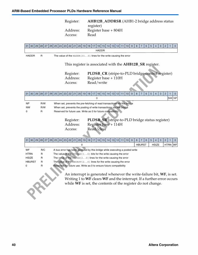
Register: AHB12B_CR (AHB1-2 bridge-control register)Address: Register base + 100HAccess: Read/write
Register: AHB12B_SR (AHB1-2 bridge-status register)Address: Register base + 800HAccess: Read/clear
An interrupt is generated whenever the write-failure bit, WF, is set. Writing 1 to WF clears WF and the interrupt. If a further error occurs while WF is set, the contents of the register do not change.
NP R/W When set, prevents the pre-fetching of read transactions via this bridge
NW R/W When set, prevents the posting of write transactions via this bridge
0 R Reserved for future use. Write as 0 for future compatibility
12345678910111213141516171819202122232425262728293031 0
NPNW0
WF R/C A bus error has been received by this bridge while executing a posted write
HTRN R The value of the HTRANS[1..0] bits for the write transaction which is causing the error
HSIZE R The value of the HSIZE[2..0] lines for the write transaction which is causing the error
HBURST R The value of the HBURST[2..0] lines for the write transaction which is causing the error
0 R Reserved for future use. Write as 0 to ensure future compatibility
12345678910111213141516171819202122232425262728293031 0
HBURST HSIZE HTRN WF0
Altera Corporation 39
ARM-Based Embedded Processor PLDs Hardware Reference Manual
PRELIM
INARY IN
FORMAT
ION
Register: AHB12B_ADDRSR (AHB1-2 bridge address status register)
Address: Register base + 804HAccess: Read
This register is associated with the AHB12B_SR register.
Register: PLDSB_CR (stripe-to-PLD bridge-control register)Address: Register base + 110HAccess: Read/write
Register: PLDSB_SR (stripe-to-PLD bridge status register)Address: Register base + 114HAccess: Read/clear
An interrupt is generated whenever the write-failure bit, WF, is set. Writing 1 to WF clears WF and the interrupt. If a further error occurs while WF is set, the contents of the register do not change.
HADDR R The value of the HADDR[31..0] lines for the write causing the error
12345678910111213141516171819202122232425262728293031 0
HADDR
NP R/W When set, prevents the pre-fetching of read transactions via this bridge
NW R/W When set, prevents the posting of write transactions via this bridge
0 R Reserved for future use. Write as 0 for future compatibility
12345678910111213141516171819202122232425262728293031 0
NPNW0
WF R/C A bus error has been received by this bridge while executing a posted write
HTRN R The value of the HTRANS[1..0] bits for the write causing the error
HSIZE R The value of the HSIZE[2..0] lines for the write causing the error
HBURST R The value of the HBURST[2..0] lines for the write causing the error
0 R Reserved for future use. Write as 0 to ensure future compatibility
12345678910111213141516171819202122232425262728293031 0
HBURST HSIZE HTRN WF0
40 Altera Corporation
ARM-Based Embedded Processor PLDs Hardware Reference Manual
PRELIM
INARY IN
FORMAT
ION
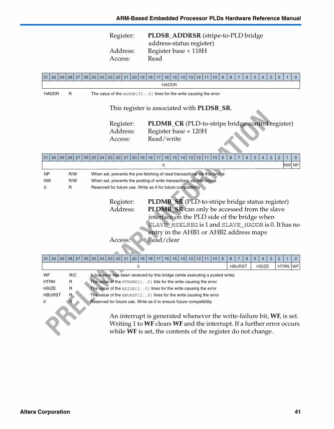
Register: PLDSB_ADDRSR (stripe-to-PLD bridge address-status register)
Address: Register base + 118HAccess: Read
This register is associated with PLDSB_SR.
Register: PLDMB_CR (PLD-to-stripe bridge-control register)Address: Register base + 120HAccess: Read/write
Register: PLDMB_SR (PLD-to-stripe bridge status register)Address: PLDMB_SR can only be accessed from the slave
interface on the PLD side of the bridge when SLAVE_HSELREG is 1 and SLAVE_HADDR is 0. It has no entry in the AHB1 or AHB2 address maps
Access: Read/clear
An interrupt is generated whenever the write-failure bit, WF, is set. Writing 1 to WF clears WF and the interrupt. If a further error occurs while WF is set, the contents of the register do not change.
HADDR R The value of the HADDR[31..0] lines for the write causing the error
12345678910111213141516171819202122232425262728293031 0
HADDR
NP R/W When set, prevents the pre-fetching of read transactions via this bridge
NW R/W When set, prevents the posting of write transactions via this bridge
0 R Reserved for future use. Write as 0 for future compatibility
12345678910111213141516171819202122232425262728293031 0
NPNW0
WF R/C A bus error has been received by this bridge (while executing a posted write)
HTRN R The value of the HTRANS[1..0] bits for the write causing the error
HSIZE R The value of the HSIZE[2..0] lines for the write causing the error
HBURST R The value of the HBURST[2..0] lines for the write causing the error
0 R Reserved for future use. Write as 0 to ensure future compatibility
12345678910111213141516171819202122232425262728293031 0
HBURST HSIZE HTRN WF0
Altera Corporation 41
ARM-Based Embedded Processor PLDs Hardware Reference Manual
PRELIM
INARY IN
FORMAT
ION
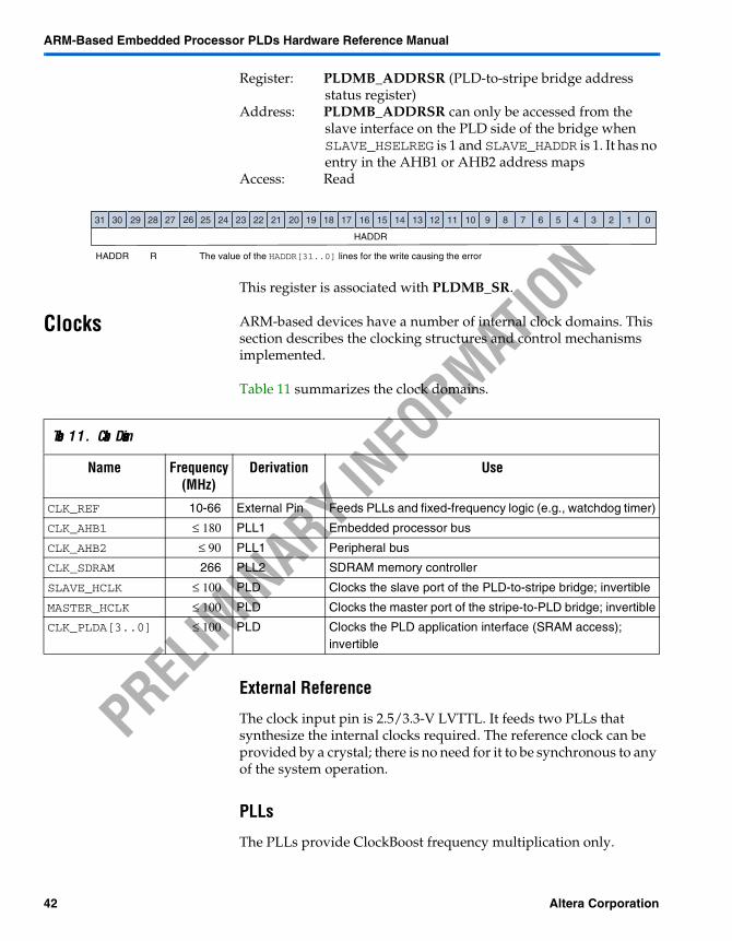
Register: PLDMB_ADDRSR (PLD-to-stripe bridge address status register)
Address: PLDMB_ADDRSR can only be accessed from the slave interface on the PLD side of the bridge when SLAVE_HSELREG is 1 and SLAVE_HADDR is 1. It has no entry in the AHB1 or AHB2 address maps
Access: Read
This register is associated with PLDMB_SR.
Clocks ARM-based devices have a number of internal clock domains. This section describes the clocking structures and control mechanisms implemented.
Table 11 summarizes the clock domains.
External Reference
The clock input pin is 2.5/3.3-V LVTTL. It feeds two PLLs that synthesize the internal clocks required. The reference clock can be provided by a crystal; there is no need for it to be synchronous to any of the system operation.
PLLs
The PLLs provide ClockBoost frequency multiplication only.
HADDR R The value of the HADDR[31..0] lines for the write causing the error
12345678910111213141516171819202122232425262728293031 0
HADDR
Table 11. Clock Domains
Name Frequency (MHz)
Derivation Use
CLK_REF 10-66 External Pin Feeds PLLs and fixed-frequency logic (e.g., watchdog timer)
CLK_AHB1 ≤ 180 PLL1 Embedded processor bus
CLK_AHB2 ≤ 90 PLL1 Peripheral bus
CLK_SDRAM 266 PLL2 SDRAM memory controller
SLAVE_HCLK ≤ 100 PLD Clocks the slave port of the PLD-to-stripe bridge; invertible
MASTER_HCLK ≤ 100 PLD Clocks the master port of the stripe-to-PLD bridge; invertible
CLK_PLDA[3..0] ≤ 100 PLD Clocks the PLD application interface (SRAM access); invertible
42 Altera Corporation
ARM-Based Embedded Processor PLDs Hardware Reference Manual
PRELIM
INARY IN
FORMAT
ION
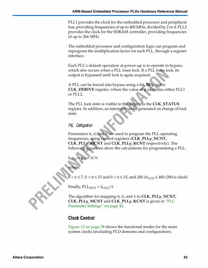
PLL1 provides the clock for the embedded processor and peripheral bus, providing frequencies of up to 400 MHz, divided by 2 or 4. PLL2 provides the clock for the SDRAM controller, providing frequencies of up to 266 MHz.
The embedded processor and configuration logic can program and reprogram the multiplication factor for each PLL, through a register interface.
Each PLL’s default operation at power-up is to operate in bypass, which also occurs when a PLL loses lock. If a PLL loses lock, its output is bypassed until lock is again acquired.
A PLL can be forced into bypass using a bit, BPy, in the CLK_DERIVE register, where the value of y identifies either PLL1 or PLL2.
The PLL lock state is visible to the stripe via the CLK_STATUS register. In addition, an interrupt can be generated on change of lock state.
PLL Configuration
Parameters M, N, and K are used to program the PLL operating frequencies, using control registers (CLK_PLLy_NCNT, CLK_PLLy_MCNT and CLK_PLLy_KCNT respectively). The following equations show the calculations for programming a PLL:
fVCO = fIN × M/N
where:
0 < K ≤ 7, 0 < M ≤ 15 and 0 < N ≤ 15, and 200 ≤fVCO ≤ 400 (300 is ideal)
Finally, PLLOUT = fVCO/K
The algorithm for mapping M, N, and K to CLK_PLLy_NCNT, CLK_PLLy_MCNT and CLK_PLLy_KCNT is given in “PLL Parameter Settings” on page 42.
Clock Control
Figure 13 on page 38 shows the functional modes for the main system clocks (excluding PLD domains and configuration).
Altera Corporation 43
ARM-Based Embedded Processor PLDs Hardware Reference Manual
PRELIM
INARY IN
FORMAT
ION
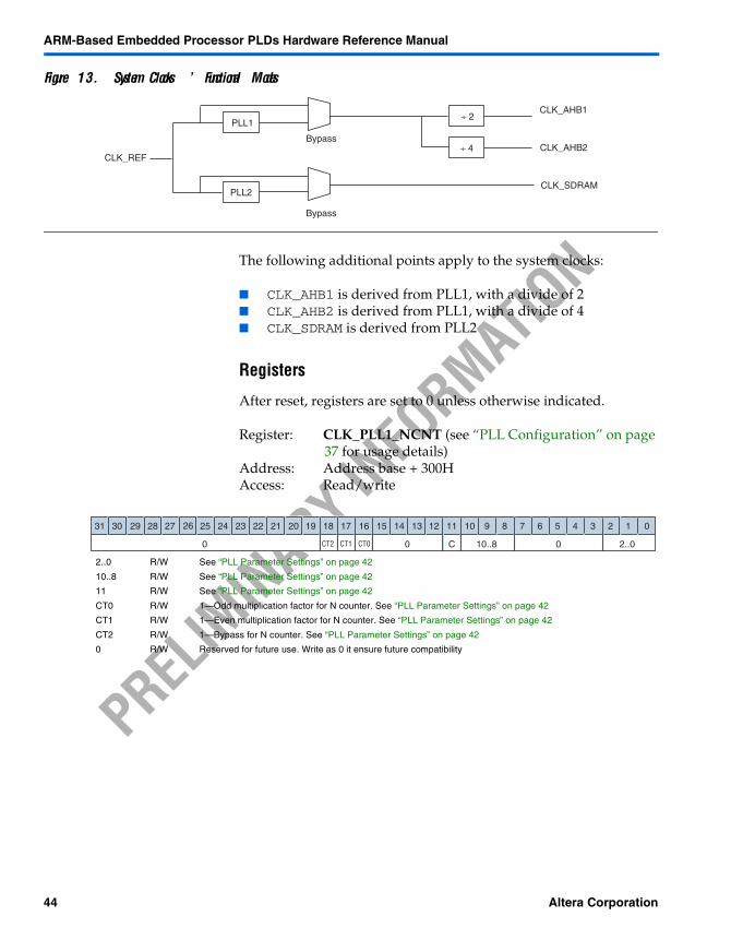
Figure 13. System Clocks’ Functional Modes
The following additional points apply to the system clocks:
CLK_AHB1 is derived from PLL1, with a divide of 2 CLK_AHB2 is derived from PLL1, with a divide of 4 CLK_SDRAM is derived from PLL2
Registers
After reset, registers are set to 0 unless otherwise indicated.
Register: CLK_PLL1_NCNT (see “PLL Configuration” on page 37 for usage details)
Address: Address base + 300HAccess: Read/write
PLL1
PLL2
÷ 2
÷ 4CLK_REF
CLK_AHB1
CLK_AHB2
CLK_SDRAM
Bypass
Bypass
2..0 R/W See “PLL Parameter Settings” on page 42
10..8 R/W See “PLL Parameter Settings” on page 42
11 R/W See “PLL Parameter Settings” on page 42
CT0 R/W 1—Odd multiplication factor for N counter. See “PLL Parameter Settings” on page 42
CT1 R/W 1—Even multiplication factor for N counter. See “PLL Parameter Settings” on page 42
CT2 R/W 1—Bypass for N counter. See “PLL Parameter Settings” on page 42
0 R/W Reserved for future use. Write as 0 it ensure future compatibility
12345678910111213141516171819202122232425262728293031 0
CT2 10..8 2..00 0 0CT1 CT0 C
44 Altera Corporation
ARM-Based Embedded Processor PLDs Hardware Reference Manual
PRELIM
INARY IN
FORMAT
ION
Register: CLK_PLL1_MCNT (see “PLL Configuration” on page 37 for usage details)
Address: Address base + 304HAccess: Read/write
Register: CLK_PLL1_KCNT (see “PLL Configuration” on page 37 for usage details)
Address: Address base + 308HAccess: Read/write
Register: CLK_PLL1_CTRLAddress: Address base + 30CHAccess: Read/writeReset value: Either 1A05H (PLL enabled)
or 1A04H (PLL disabled)
2..0 R/W See “PLL Parameter Settings” on page 42
10..8 R/W See “PLL Parameter Settings” on page 42
11 R/W See “PLL Parameter Settings” on page 42
CT0 R/W 1—Odd multiplication factor for M counter. See “PLL Parameter Settings” on page 42
CT1 R/W 1—Even multiplication factor for M counter. See “PLL Parameter Settings” on page 42
CT2 R/W 1—Bypass for M counter. See “PLL Parameter Settings” on page 42
0 R/W Reserved for future use. Write as 0 it ensure future compatibility
12345678910111213141516171819202122232425262728293031 0
CT2 10..8 2..00 0 0CT1 CT0 C
1..0 R/W See “PLL Parameter Settings” on page 42
9..8 R/W See “PLL Parameter Settings” on page 42
10 R/W See “PLL Parameter Settings” on page 42
CT0 R/W 1—Odd multiplication factor for K counter. See “PLL Parameter Settings” on page 42
CT1 R/W 1—Even multiplication factor for K counter. See “PLL Parameter Settings” on page 42
CT2 R/W 1—Bypass for K counter. See “PLL Parameter Settings” on page 42
0 R/W Reserved for future use. Write as 0 it ensure future compatibility
12345678910111213141516171819202122232425262728293031 0
0 0 0CT2 CT1 CT0 C 9..8 1..0
P R/W 1—PLL enabled
CTRL R/W Reserved. Write as 00110100000010
0 R/W Reserved for future use. Write as 0 it ensure future compatibility
12345678910111213141516171819202122232425262728293031 0
0 PCTRL
Altera Corporation 45
ARM-Based Embedded Processor PLDs Hardware Reference Manual
PRELIM
INARY IN
FORMAT
ION
Register: CLK_PLL2_NCNT (see “PLL Configuration” on page 37 for usage details)
Address: Address base + 310HAccess: Read/write
Register: CLK_PLL2_MCNT (see “PLL Configuration” on page 37 for usage details)
Address: Address Base + 314HAccess: Read/write
Register: CLK_PLL2_KCNT (see “PLL Configuration” on page 37 for usage details)
Address: Address base + 318HAccess: Read/write
2..0 R/W See “PLL Parameter Settings” on page 42
10..8 R/W See “PLL Parameter Settings” on page 42
11 R/W See “PLL Parameter Settings” on page 42
CT0 R/W 1—Odd multiplication factor for N counter. See “PLL Parameter Settings” on page 42
CT1 R/W 1—Even multiplication factor for N counter. See “PLL Parameter Settings” on page 42
CT2 R/W 1—Bypass for N counter. See “PLL Parameter Settings” on page 42
0 R/W Reserved for future use. Write as 0 it ensure future compatibility
12345678910111213141516171819202122232425262728293031 0
CT2 10..8 2..00 0 0CT1 CT0 C
2..0 R/W See “PLL Parameter Settings” on page 42
10..8 R/W See “PLL Parameter Settings” on page 42
11 R/W See “PLL Parameter Settings” on page 42
CT0 R/W 1—Odd multiplication factor for M counter. See “PLL Parameter Settings” on page 42
CT1 R/W 1—Even multiplication factor for M counter. See “PLL Parameter Settings” on page 42
CT2 R/W 1—Bypass for M counter. See “PLL Parameter Settings” on page 42
0 R/W Reserved for future use. Write as 0 it ensure future compatibility
12345678910111213141516171819202122232425262728293031 0
CT2 10..8 2..00 0 0CT1 CT0 C
1..0 R/W See “PLL Parameter Settings” on page 42
9..8 R/W See “PLL Parameter Settings” on page 42
10 R/W See “PLL Parameter Settings” on page 42
CT0 R/W 1—Odd multiplication factor for K counter. See “PLL Parameter Settings” on page 42
CT1 R/W 1—Even multiplication factor for K counter. See “PLL Parameter Settings” on page 42
CT2 R/W 1—Bypass for K counter. See “PLL Parameter Settings” on page 42
0 R/W Reserved for future use. Write as 0 it ensure future compatibility
12345678910111213141516171819202122232425262728293031 0
0 0 0CT2 CT1 CT0 C 9..8 1..0
46 Altera Corporation
ARM-Based Embedded Processor PLDs Hardware Reference Manual
PRELIM
INARY IN
FORMAT
ION
Register: CLK_PLL2_CTRLAddress: Address base + 31CHAccess: Read/writeReset value: Either 1A05H (PLL enabled)
or 1A04H (PLL disabled)
Register: CLK_DERIVEAddress: Register base + 320HAccess: Read/writeReset value: 3010H
Register: CLK_STATUSAddress: Register base + 324HAccess: Read/clear
The clock module generates an interrupt when either C1 or C2 is set.
P R/W 1—PLL enabled
CTRL R/W Reserved. Write as 00110100000010
0 R/W Reserved for future use. Write as 0 it ensure future compatibility
12345678910111213141516171819202122232425262728293031 0
0 PCTRL
0 R Reserved for future use. Write as 0 to ensure future compatibility
1 W Reserved. Write as 1 to ensure correct operation
BP2 R/W 1—Force bypass of PLL2
BP1 R/W 1—Force bypass of PLL1
12345678910111213141516171819202122232425262728293031 0
BP2BP1 0 00 1
L1 R PLL1 lock status
L2 R PLL2 lock status
C1 R/C 1—PLL1 lock changed
C2 R/C 1—PLL2 lock changed
P1 R 1—PLL1 not bypassed
P2 R 1—PLL2 not bypassed
0 R Reserved for future use. Write as 0 to ensure future compatibility
12345678910111213141516171819202122232425262728293031 0
0 C2 C1 L2 L1P1P2
Altera Corporation 47
ARM-Based Embedded Processor PLDs Hardware Reference Manual
PRELIM
INARY IN
FORMAT
ION
PLL Parameter Settings
For either of the PLLs, M, N and K are mapped to the appropriate parameter register using one of the following procedures:
For the M and N parameters:
For the K parameter:
Subsequently, for K, M or N parameters:
In the procedures above, y corresponds to the PLL being programmed and x is M, N, or K, corresponding to the parameter; z is the actual value of the parameter.
For example, if the value of M for PLL1 is 15 (1111):
Therefore, register CLK_PLL1_MCNT has the value 40807H.
CLK_PLLy_xCNT[2..0] = z[3..1]
CLK_PLLy_xCNT[10..8] = z([3..1] + z[0])
CLK_PLLy_xCNT[11] = carry bit from the previous addition
CLK_PLLy_xCNT[1..0] = z[2..1]
CLK_PLLy_xCNT[9..8] = z([2..1] + z[0])
CLK_PLLy_xCNT[10] = carry bit from the previous addition
CLK_PLLy_xCNT[18] = 1, if z is odd
CLK_PLLy_xCNT[17] = 1, if z is even
CLK_PLLy_xCNT[16] = 1, if z is 1 (PLL calculation is pointless)
CLK_PLL1_MCNT[2..0] = 111
CLK_PLL1_MCNT[10..8] = 111 + 1 = 000, with carry 1
CLK_PLL1_MCNT[11] = 1 (carry from previous addition)
CLK_PLL1_MCNT[18] = 1 (15 is an odd number)
CLK_PLL1_MCNT[17] = 0 (M is not even)
CLK_PLL1_MCNT[16] = 0 (M is 15, not 1)
48 Altera Corporation
ARM-Based Embedded Processor PLDs Hardware Reference Manual
PRELIM
INARY IN
FORMAT
ION
Similarly, if the value of K for PLL2 is 2 (010):
Therefore, register CLK_PLL2_KCNT has the value 20101H.
Profiling Register
A 32-bit clock module register counts the number of processor cycles since reset. This stops counting when the embedded processor is in debug mode (i.e. when DEBUG_ACK is active).
Register: CLK_AHB1_COUNTAddress: Register base + 328HAccess: Read only
CLK_PLL2_KCNT[1..0] = 01
CLK_PLL2_KCNT[9..8] = 01 + 0 = 01, with no carry
CLK_PLL2_KCNT[10] = 0 (carry from previous addition)
CLK_PLL2_KCNT[18] = 0 (2 is not odd)
CLK_PLL2_KCNT[17] = 1 (2 is an even number)
CLK_PLL2_KCNT[16] = 0 (K is 2, not 1)
12345678910111213141516171819202122232425262728293031 0
Count of processor cycles since reset
Altera Corporation 49
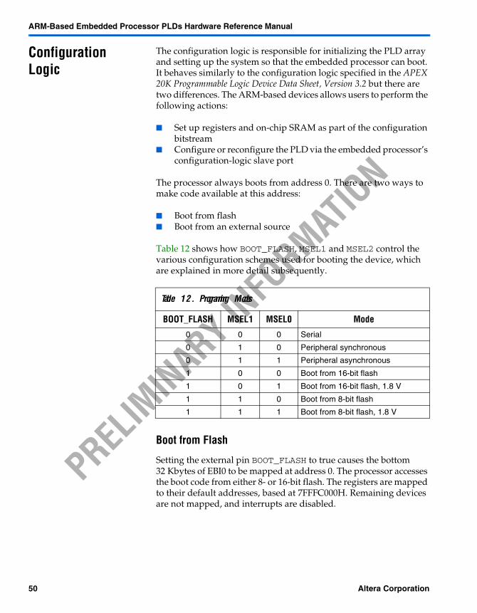
ARM-Based Embedded Processor PLDs Hardware Reference Manual
PRELIM
INARY IN
FORMAT
ION
Configuration Logic
The configuration logic is responsible for initializing the PLD array and setting up the system so that the embedded processor can boot. It behaves similarly to the configuration logic specified in the APEX 20K Programmable Logic Device Data Sheet, Version 3.2 but there are two differences. The ARM-based devices allows users to perform the following actions:
Set up registers and on-chip SRAM as part of the configuration bitstream
Configure or reconfigure the PLD via the embedded processor’s configuration-logic slave port
The processor always boots from address 0. There are two ways to make code available at this address:
Boot from flash Boot from an external source
Table 12 shows how BOOT_FLASH, MSEL1 and MSEL2 control the various configuration schemes used for booting the device, which are explained in more detail subsequently.
Boot from Flash
Setting the external pin BOOT_FLASH to true causes the bottom 32 Kbytes of EBI0 to be mapped at address 0. The processor accesses the boot code from either 8- or 16-bit flash. The registers are mapped to their default addresses, based at 7FFFC000H. Remaining devices are not mapped, and interrupts are disabled.
Table 12. Programming Modes
BOOT_FLASH MSEL1 MSEL0 Mode
0 0 0 Serial
0 1 0 Peripheral synchronous
0 1 1 Peripheral asynchronous
1 0 0 Boot from 16-bit flash
1 0 1 Boot from 16-bit flash, 1.8 V
1 1 0 Boot from 8-bit flash
1 1 1 Boot from 8-bit flash, 1.8 V
50 Altera Corporation
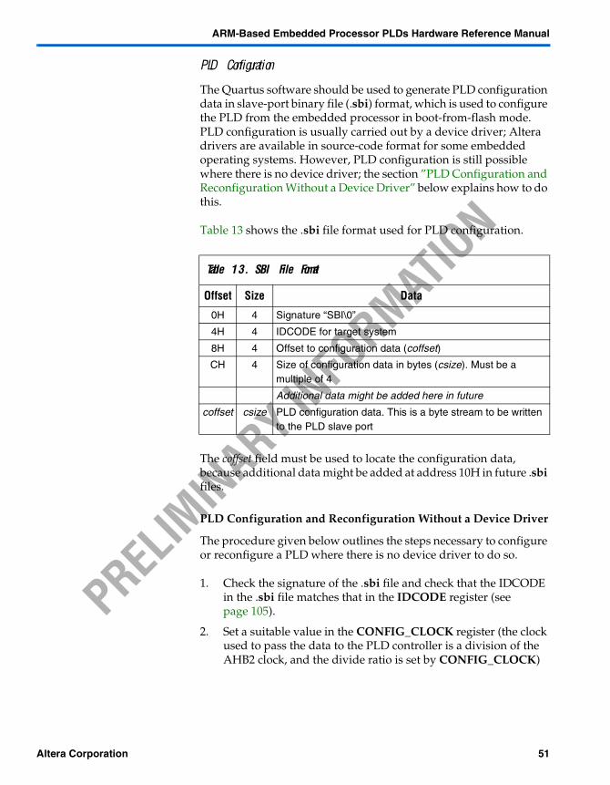
ARM-Based Embedded Processor PLDs Hardware Reference Manual
PRELIM
INARY IN
FORMAT
ION
PLD Configuration
The Quartus software should be used to generate PLD configuration data in slave-port binary file (.sbi) format, which is used to configure the PLD from the embedded processor in boot-from-flash mode. PLD configuration is usually carried out by a device driver; Altera drivers are available in source-code format for some embedded operating systems. However, PLD configuration is still possible where there is no device driver; the section ”PLD Configuration and Reconfiguration Without a Device Driver” below explains how to do this.
Table 13 shows the .sbi file format used for PLD configuration.
The coffset field must be used to locate the configuration data, because additional data might be added at address 10H in future .sbi files.
PLD Configuration and Reconfiguration Without a Device Driver
The procedure given below outlines the steps necessary to configure or reconfigure a PLD where there is no device driver to do so.
1. Check the signature of the .sbi file and check that the IDCODE in the .sbi file matches that in the IDCODE register (see page 105).
2. Set a suitable value in the CONFIG_CLOCK register (the clock used to pass the data to the PLD controller is a division of the AHB2 clock, and the divide ratio is set by CONFIG_CLOCK)
Table 13. SBI File Format
Offset Size Data
0H 4 Signature “SBI\0”
4H 4 IDCODE for target system
8H 4 Offset to configuration data (coffset)
CH 4 Size of configuration data in bytes (csize). Must be a multiple of 4
Additional data might be added here in future
coffset csize PLD configuration data. This is a byte stream to be written to the PLD slave port
Altera Corporation 51
ARM-Based Embedded Processor PLDs Hardware Reference Manual
PRELIM
INARY IN
FORMAT
ION
3. Read the CONFIG_CONTROL register to check whether the configuration slave port is locked. If the lock bit, LK, is set, write the magic value 554E4C4BH to the CONFIG_UNLOCK register to unset it
4. Set the configuration bit, CO, of the CONFIG_CONTROL register
5. Write all the configuration data from the file to the CONFIG_DATA register. A new word of data should be written whenever the busy bit, B, is not set (B indicates whether the buffer is empty or being operated on). If data is written to CONFIG_DATA while B is set, the slave inserts wait states
6. Wait for the configuration port to clear the configuration bit, CO, in CONFIG_CONTROL
7. If the error bit, E, in CONFIG_CONTROL is set at any time, or if CO is not cleared, configuration was unsuccessful
8. Optionally, lock the configuration logic by setting the lock bit, LK, of the CONFIG_CONTROL register
Boot from External Configuration Source
When BOOT_FLASH is false, the embedded processor is held in reset while the PLD is being configured. The configuration bitstream contains register writes to enable writable memory (such as on-chip SRAM) at address 0, and to write code into this memory, followed by PLD configuration data. Finally, the bitstream writes to the boot control register, BOOT_CR to release the processor from reset.
The processor is not released from reset until the configuration logic has entered user mode.
Figure 14 on page 47 shows how the embedded processor boots from an external source.
52 Altera Corporation
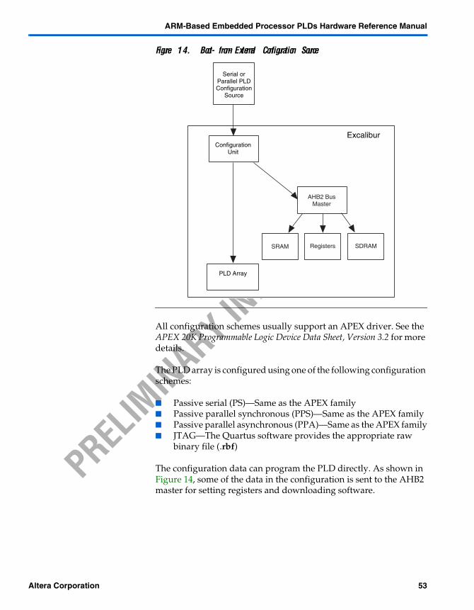
ARM-Based Embedded Processor PLDs Hardware Reference Manual
PRELIM
INARY IN
FORMAT
ION
Figure 14. Boot-from-External Configuration Source
All configuration schemes usually support an APEX driver. See the APEX 20K Programmable Logic Device Data Sheet, Version 3.2 for more details.
The PLD array is configured using one of the following configuration schemes:
Passive serial (PS)—Same as the APEX family Passive parallel synchronous (PPS)—Same as the APEX family Passive parallel asynchronous (PPA)—Same as the APEX family JTAG—The Quartus software provides the appropriate raw
binary file (.rbf)
The configuration data can program the PLD directly. As shown in Figure 14, some of the data in the configuration is sent to the AHB2 master for setting registers and downloading software.
Serial orParallel PLDConfiguration
Source
Excalibur
PLD Array
ConfigurationUnit
SRAM Registers SDRAM
AHB2 BusMaster
Altera Corporation 53
ARM-Based Embedded Processor PLDs Hardware Reference Manual
PRELIM
INARY IN
FORMAT
ION
PLD Configuration
Raw binary files (.rbf), tabular text files (.ttf) or intel-format .hexout formats produced by the Quartus software are acceptable for PLD configuration via the PLD controller interface. In addition, programmer output files (.pof) produced by the Quartus software can be used to program external configuration devices connected to this interface.
Registers
Register: CONFIG_CONTROL (configuration control register)Address: Register base + 140HAccess: Read/write
The lock bit, LK, can be used to prevent inadvertent reconfiguration of the PLD. When LK is set, writing to CONFIG_CONTROL, CONFIG_CLOCK, or CONFIG_DATA causes a bus error and does not change the register contents. LK is reset by writing the magic number to CONFIG_UNLOCK, or system reset.
Setting the configure bit, CO, to 1 (when it was previously 0) initiates PLD configuration. CO is set to 0 when configuration is complete, whether successfully or with an error condition.
If CO is set while the PLD is being configured (either via external configuration pins or via JTAG), the error bit, E, is set, and CO is reset.
LK R/W Lock. When set, writes to this register cause a bus error instead of changing the register contents
CO R/W Configure. When set, indicates that the PLD is being configured via the slave controller. The slave controller clears this bit when configuration is complete
B R Busy. When set, either the data register is not ready to accept data (and inserts wait states if written to) or the PLD controller is resetting in preparation for configuration
PC R When set, the PLD is configured and in user mode
E R Error. When set, indicates that (re)configuration was not possible for one of the reasons below.– External configuration prevents reconfiguration– The PLD is being configured via JTAG– There was an error in the PLD bitstream– CONFIG_CLOCK value is 0This bit is latching and is cleared by setting CO while ES is 0
ES R Error source. These (non-latching) bits indicate that reconfiguration is not currently possible for one or more reasons. The value presented is the logical or of the following values:001—PLD being configured via JTAG010—CONFIG_CLOCK value is zero100—PLD being configured via external configuration interface
0 R Reserved for future use. Write as 0 to ensure future compatibility
12345678910111213141516171819202122232425262728293031 0
0 ES E PC B CO LK
54 Altera Corporation
ARM-Based Embedded Processor PLDs Hardware Reference Manual
PRELIM
INARY IN
FORMAT
ION
Immediately after CO is set, the busy bit, B, is set, and is cleared when the PLD controller is ready to receive data.
When CONFIG_CLOCK has the value 0, any attempt to set CO to 1 (when it was previously 0) is ignored, and results in E being set.
Setting CO to 0 (when it was previously 1) using a register-write aborts the configuration and sets E.
Register: CONFIG_CLOCK (configuration clock register)Address: Register base + 144HAccess: Read/write
The clock divide ratio allows a valid clock to be generated from the AHB2 clock to drive the PLD control logic in parallel-synchronous mode. The maximum clock frequency for the PLD controller is 16 MHz. If the divide ratio is set to provide a higher speed, or not to provide a clock at all, the results are undefined. If CONFIG_CLOCK is written during configuration via the slave port (i.e., CO is set), the write is ignored.
For an AHB2 clock speed of 60 MHz, a divide ratio of 3 produces a PLD download-clock of 10 MHz.
Register: CONFIG_DATA (embedded controller data register)Address: Register base + 148HAccess: Write
Data written to CONFIG_DATA when the configure bit, CO, in CONFIG_CONTROL is not set is ignored. Data written to CONFIG_DATA is stored in a holding register and then loaded into the PLD configuration logic in parallel-synchronous mode.
RATIO R/W Half the divide ratio applied to AHB2 clock to generate the PLD download clock. No clock is generated when this has the value 0
0 R Reserved for future use. Write as 0 to ensure future compatibility
12345678910111213141516171819202122232425262728293031 0
0 RATIO
DATA W Data written to PLD configuration logic
12345678910111213141516171819202122232425262728293031 0
DATA
Altera Corporation 55
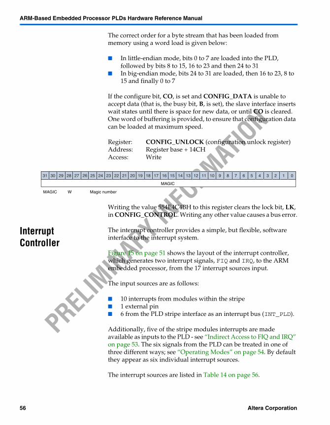
ARM-Based Embedded Processor PLDs Hardware Reference Manual
PRELIM
INARY IN
FORMAT
ION
The correct order for a byte stream that has been loaded from memory using a word load is given below:
In little-endian mode, bits 0 to 7 are loaded into the PLD, followed by bits 8 to 15, 16 to 23 and then 24 to 31
In big-endian mode, bits 24 to 31 are loaded, then 16 to 23, 8 to 15 and finally 0 to 7
If the configure bit, CO, is set and CONFIG_DATA is unable to accept data (that is, the busy bit, B, is set), the slave interface inserts wait states until there is space for new data, or until CO is cleared. One word of buffering is provided, to ensure that configuration data can be loaded at maximum speed.
Register: CONFIG_UNLOCK (configuration unlock register)Address: Register base + 14CHAccess: Write
Writing the value 554E4C4BH to this register clears the lock bit, LK, in CONFIG_CONTROL. Writing any other value causes a bus error.
Interrupt Controller
The interrupt controller provides a simple, but flexible, software interface to the interrupt system.
Figure 15 on page 51 shows the layout of the interrupt controller, which generates two interrupt signals, FIQ and IRQ, to the ARM embedded processor, from the 17 interrupt sources input.
The input sources are as follows:
10 interrupts from modules within the stripe 1 external pin 6 from the PLD stripe interface as an interrupt bus (INT_PLD).
Additionally, five of the stripe modules interrupts are made available as inputs to the PLD - see “Indirect Access to FIQ and IRQ” on page 53. The six signals from the PLD can be treated in one of three different ways; see “Operating Modes” on page 54. By default they appear as six individual interrupt sources.
The interrupt sources are listed in Table 14 on page 56.
MAGIC W Magic number
12345678910111213141516171819202122232425262728293031 0
MAGIC
56 Altera Corporation
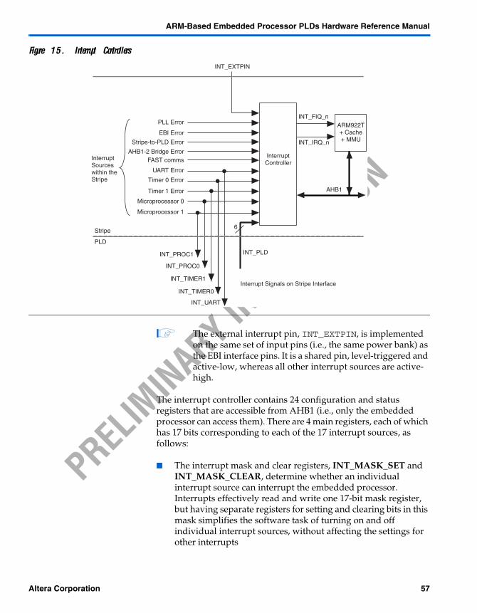
ARM-Based Embedded Processor PLDs Hardware Reference Manual
PRELIM
INARY IN
FORMAT
ION
Figure 15. Interrupt Controllers
The external interrupt pin, INT_EXTPIN, is implemented on the same set of input pins (i.e., the same power bank) as the EBI interface pins. It is a shared pin, level-triggered and active-low, whereas all other interrupt sources are active-high.
The interrupt controller contains 24 configuration and status registers that are accessible from AHB1 (i.e., only the embedded processor can access them). There are 4 main registers, each of which has 17 bits corresponding to each of the 17 interrupt sources, as follows:
The interrupt mask and clear registers, INT_MASK_SET and INT_MASK_CLEAR, determine whether an individual interrupt source can interrupt the embedded processor. Interrupts effectively read and write one 17-bit mask register, but having separate registers for setting and clearing bits in this mask simplifies the software task of turning on and off individual interrupt sources, without affecting the settings for other interrupts
InterruptController
Stripe6
PLD
INT_EXTPIN
ARM922T+ Cache+ MMU
PLL Error
EBI Error
Stripe-to-PLD Error
AHB1-2 Bridge ErrorFAST comms
INT_UART
INT_TIMER0
INT_TIMER1
INT_PROC0
INT_PROC1
InterruptSourceswithin theStripe
AHB1
INT_PLD
Interrupt Signals on Stripe Interface
INT_FIQ_n
INT_IRQ_n
UART Error
Timer 0 Error
Timer 1 Error
Microprocessor 0
Microprocessor 1
Altera Corporation 57
ARM-Based Embedded Processor PLDs Hardware Reference Manual
PRELIM
INARY IN
FORMAT
ION
The interrupt request and source registers, INT_REQUEST_STATUS and INT_SOURCE_STATUS, provide the status of each interrupt source before and after masking respectively
Each of the 17 interrupt sources also has its own priority register, INT_PRIORITY_x (where x ranges from 0 to 16). Each contains a 6-bit priority value, PRI, and a ‘generate FIQ if active’ bit, FQ, for each interrupt source. The registers determine subsequent interrupt activity:
Whether that particular interrupt source, when requesting, triggers an FIQ or IRQ interrupt signal to the processor
What value is present in the interrupt identification register, INT_ID, when one or more interrupts are requesting; see “Interrupt Priority” on page 52
A requesting interrupt source is one for which the interrupt source is active and the appropriate mask bit has been set by the INT_MASK_SET register.
IRQ and FIQ Requests to the Processor
The IRQ interrupt to the embedded processor becomes active when any requesting interrupt source has a priority value, PRI, that is non-zero but less than the maximum value, 3FH.
In default operating mode (see “Operating Modes” on page 54), the FIQ interrupt to the embedded processor becomes active when either PRI in INT_PRIORITY_x is 3FH, or FQ is set. This signifies that the requesting interrupt source has a maximum priority value.
The FQ bits in the interrupt priority registers have no effect on IRQ interrupt generation.
Interrupt signals to the processor (FIQ and/or IRQ) remain active for as long as the interrupting source is active, provided that the register settings are not changed to disable interrupts.
Interrupt Priority
On receiving an interrupt, the embedded processor first establishes its source. If several interrupts are active, the embedded processor also has to decide which is the highest priority.The priority scheme implemented in the interrupt controller facilitates this.
58 Altera Corporation
ARM-Based Embedded Processor PLDs Hardware Reference Manual
PRELIM
INARY IN
FORMAT
ION
To implement the priority scheme, the user writes relative priority values to each of the 17 priority registers at system initialization. Each source is usually assigned a unique priority value between 1H and 3FH. Prioritization logic in the interrupt controller constantly compares the priority values within all the priority registers (PRI in INT_PRIORITY_x) to discover which interrupts are pending, and provides the value of the highest in the interrupt identification register INT_ID. An interrupt service routine then reads this register to quickly identify the interrupt source.
The value of the interrupt identity register, INT_ID, changes as soon as interrupting sources change.
If FQ in INT_PRIORITY_x for a requesting interrupt source is set, but its priority value, PRI, is 0H, the interrupt controller generates an FIQ interrupt but does not update the interrupt identity register, INT_ID.
Indirect Access to FIQ and IRQ
In default operating mode, the interrupt mode register, INT_MODE, is set to 3H. The following settings apply (see also Table 14 on page 56):
The INT_PLD bus from the PLD-stripe interface is configured as six individual interrupt sources
INT_PLD[0] is set (and enabled) to trigger FIQ INT_PLD[5:1] are each set (and enabled) to trigger IRQ
This effectively gives the user indirect access to the IRQ and FIQ interrupt inputs to the processor, with INT_PLD[0] behaving as FIQ and any one of INT_PLD[5] through INT_PLD[1] behaving as IRQ. This allows users to implement their own interrupt control scheme in the PLD, if required. In addition, because this is the default mode, users are not obliged to disable the interrupt controller within the stripe. This is particularly suited to ARM-based ASIC prototyping, where none of the stripe modules are required, other than the embedded processor.
FIQ and IRQ interrupt signals to the processor are never directly accessible, for the following reasons:
INT_PLD signals are always active high INT_PLD signals are always passed through synchronizing
D-types within the stripe In default mode, INT_PLD[5] to INT_PLD[1] are logically
OR-ed together to produce IRQ
Altera Corporation 59
ARM-Based Embedded Processor PLDs Hardware Reference Manual
PRELIM
INARY IN
FORMAT
ION
To implement an interrupt controller in the PLD instead of using the stripe interrupt controller, but still use some of the other modules within the stripe (such as the UART or timer), the interrupt outputs from these modules are made available as inputs to the PLD from the stripe interface. These five interrupt lines are shown in Figure 15 on page 51.
Operating Modes
Three operating modes are provided, to control how the six INT_PLD signals from the PLD are treated:
As six individual interrupts (the default mode) As a single interrupt request, using a six-bit priority value As a single interrupt request, using a five-bit priority value
together with one individual interrupt
These modes are controlled by the 2-bit MODE value in the interrupt mode register, INT_MODE. The operating mode is not usually changed by the user during system operation, other than at system initialization. However, the two non-default modes alter the operation of some of the registers. The interrupt controller operating modes are described in ”Six Individual Interrupts”.
Six Individual Interrupts
This is the default mode at system reset. Each of the six interrupts has its own priority register (INT_PRIORITY_0 to INT_PRIORITY_5) and its own mask and status bits in the four main mask and status registers. Each interrupt is configured to generate FIQ or IRQ as appropriate. The contents of the PLD interrupt priority register, INT_PLD_PRIORITY, are undefined in default mode.
This mode is probably the most likely to be used for applications, particularly where only a maximum of six interrupts is required from the PLD. For applications requiring more than six interrupt sources from the PLD, one of the following two modes might be more appropriate.
60 Altera Corporation
ARM-Based Embedded Processor PLDs Hardware Reference Manual
PRELIM
INARY IN
FORMAT
ION
Six-Bit Priority Value
In this mode, INT_PLD[5:0] is taken to be a six-bit encoded interrupt priority, whose value is one of the following:
0H—Signifying no interrupt from the PLD A non-zero value—Signifying a requesting interrupt with
priority ranging from 1H to 3FH
The requesting interrupt priority is compared with the other requesting interrupt priorities from modules in the stripe, to produce IRQ or FIQ requests and to determine the value of the interrupt identity register, INT_ID.
Bits P5 through P0 of the interrupt mask and clear registers, INT_MASK_SET and INT_MASK_CLEAR, together with the interrupt priority registers, INT_PRIORITY_5 through INT_PRIORITY_0, have no effect in this mode.
Bits P5 through P0 of the interrupt source and request registers, INT_SOURCE_STATUS and INT_REQUEST_STATUS, have no effect in this mode. Instead, the PLD interrupt priority register, INT_PLD_PRIORITY, contains the 6-bit priority value that the INT_PLD bus is requesting.
This mode allows up to 63 individual interrupts in the PLD to be encoded by user logic in the PLD, therefore polling is not required to identify an interrupt source.
Five-Bit Priority Value Plus Individual Interrupt
In this mode, INT_PLD[5] through INT_PLD[1] are treated as the most significant bits of a single six-bit encoded interrupt priority; and INT_PLD[0] is treated as an individual interrupt.
The least-significant bit of the six-bit encoded priority value is always 0, affecting the effective values the PLD can signal to the interrupt controller priority logic using INT_PLD[5:1]. These are listed below:
0H—Signifying no interrupt from the PLD A non-zero even value—Signifying a requesting interrupt with
priority ranging from 2H to 3EH
Altera Corporation 61
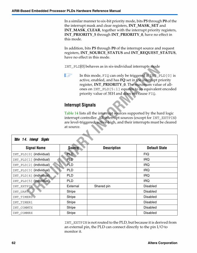
ARM-Based Embedded Processor PLDs Hardware Reference Manual
PRELIM
INARY IN
FORMAT
ION
In a similar manner to six-bit priority mode, bits P5 through P0 of the the interrupt mask and clear registers, INT_MASK_SET and INT_MASK_CLEAR, together with the interrupt priority registers, INT_PRIORITY_5 through INT_PRIORITY_0, have no effect in this mode.
In addition, bits P5 through P0 of the interrupt source and request registers, INT_SOURCE_STATUS and INT_REQUEST_STATUS, have no effect in this mode.
INT_PLD[0] behaves as in six-individual interrupts mode
In this mode, FIQ can only be triggered if INT_PLD[0] is active, enabled, and has FQ set in the interrupt priority register, INT_PRIORITY_0. The maximum value of all-ones on INT_PLD[5:1] equates to an equivalent encoded priority value of 3EH and does not cause FIQ.
Interrupt Signals
Table 14 lists all the interrupt sources supported by the hard logic interrupt controller. All interrupt sources (except for INT_EXTPIN) are level-triggered, active-high, and their interrupts must be cleared at source.
INT_EXTPIN is not routed to the PLD, but because it is derived from an external pin, the PLD can connect directly to the pin I/O to monitor it.
Table 14. Interrupt Signals
Signal Name Source Description Default State
INT_PLD[0] (individual) PLD FIQ
INT_PLD[1] (individual) PLD IRQ
INT_PLD[2] (individual) PLD IRQ
INT_PLD[3] (individual) PLD IRQ
INT_PLD[4] (individual) PLD IRQ
INT_PLD[5] (individual) PLD IRQ
INT_EXTPIN External Shared pin Disabled
INT_UART Stripe Disabled
INT_TIMER0 Stripe Disabled
INT_TIMER1 Stripe Disabled
INT_COMMTX Stripe Disabled
INT_COMMRX Stripe Disabled
62 Altera Corporation
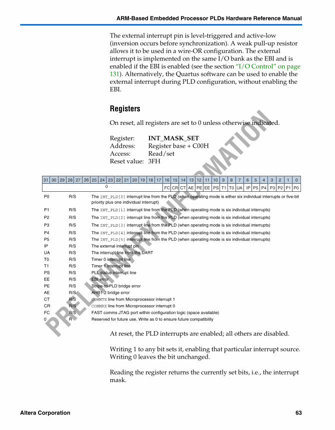
ARM-Based Embedded Processor PLDs Hardware Reference Manual
PRELIM
INARY IN
FORMAT
ION
The external interrupt pin is level-triggered and active-low (inversion occurs before synchronization). A weak pull-up resistor allows it to be used in a wire-OR configuration. The external interrupt is implemented on the same I/O bank as the EBI and is enabled if the EBI is enabled (see the section “I/O Control” on page 131). Alternatively, the Quartus software can be used to enable the external interrupt during PLD configuration, without enabling the EBI.
Registers
On reset, all registers are set to 0 unless otherwise indicated.
Register: INT_MASK_SETAddress: Register base + C00HAccess: Read/setReset value: 3FH
At reset, the PLD interrupts are enabled; all others are disabled.
Writing 1 to any bit sets it, enabling that particular interrupt source. Writing 0 leaves the bit unchanged.
Reading the register returns the currently set bits, i.e., the interrupt mask.
P0 R/S The INT_PLD[0] interrupt line from the PLD (when operating mode is either six individual interrupts or five-bit priority plus one individual interrupt)
P1 R/S The INT_PLD[1] interrupt line from the PLD (when operating mode is six individual interrupts)
P2 R/S The INT_PLD[2] interrupt line from the PLD (when operating mode is six individual interrupts)
P3 R/S The INT_PLD[3] interrupt line from the PLD (when operating mode is six individual interrupts)
P4 R/S The INT_PLD[4] interrupt line from the PLD (when operating mode is six individual interrupts)
P5 R/S The INT_PLD[5] interrupt line from the PLD (when operating mode is six individual interrupts)
IP R/S The external interrupt pin
UA R/S The interrupt line from the UART
T0 R/S Timer 0 interrupt line
T1 R/S Timer 1 interrupt line
PS R/S PLL status interrupt line
EE R/S EBI error
PE R/S Stripe-to-PLD bridge error
AE R/S AHB1-2 bridge error
CT R/S COMMTX line from Microprocessor interrupt 1
CR R/S COMMRX line from Microprocessor interrupt 0
FC R/S FAST comms JTAG port within configuration logic (space available)
0 R Reserved for future use. Write as 0 to ensure future compatibility
12345678910111213141516171819202122232425262728293031 0
0 CR CT PE EE PS T1 T0 UA IP P5 P4 P3 P2 P1 P0AEFC
Altera Corporation 63
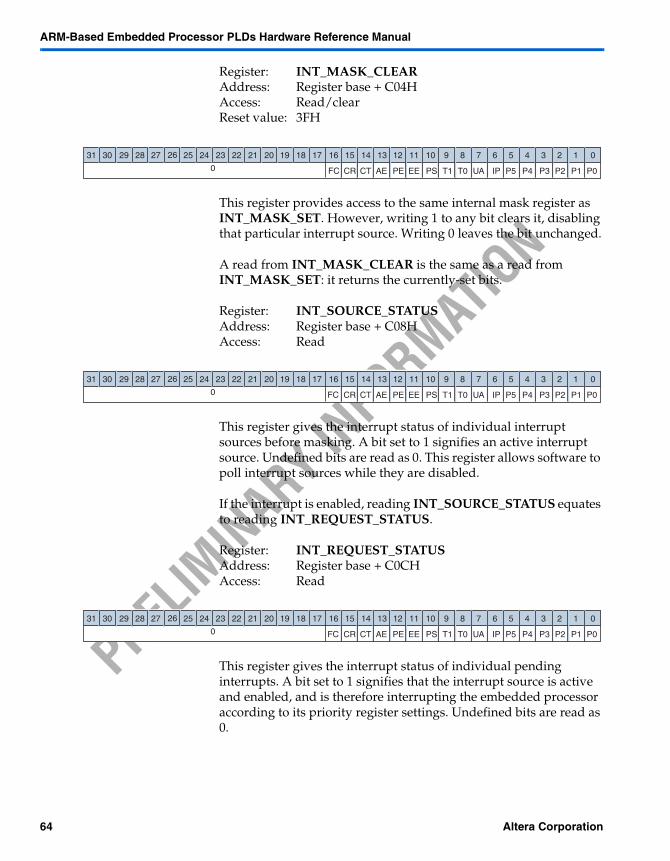
ARM-Based Embedded Processor PLDs Hardware Reference Manual
PRELIM
INARY IN
FORMAT
ION
Register: INT_MASK_CLEARAddress: Register base + C04HAccess: Read/clearReset value: 3FH
This register provides access to the same internal mask register as INT_MASK_SET. However, writing 1 to any bit clears it, disabling that particular interrupt source. Writing 0 leaves the bit unchanged.
A read from INT_MASK_CLEAR is the same as a read from INT_MASK_SET: it returns the currently-set bits.
Register: INT_SOURCE_STATUSAddress: Register base + C08HAccess: Read
This register gives the interrupt status of individual interrupt sources before masking. A bit set to 1 signifies an active interrupt source. Undefined bits are read as 0. This register allows software to poll interrupt sources while they are disabled.
If the interrupt is enabled, reading INT_SOURCE_STATUS equates to reading INT_REQUEST_STATUS.
Register: INT_REQUEST_STATUSAddress: Register base + C0CHAccess: Read
This register gives the interrupt status of individual pending interrupts. A bit set to 1 signifies that the interrupt source is active and enabled, and is therefore interrupting the embedded processor according to its priority register settings. Undefined bits are read as 0.
12345678910111213141516171819202122232425262728293031 0
0 CR CT PE EE PS T1 T0 UA IP P5 P4 P3 P2 P1 P0AEFC
12345678910111213141516171819202122232425262728293031 0
0 CR CT PE EE PS T1 T0 UA IP P5 P4 P3 P2 P1 P0AEFC
12345678910111213141516171819202122232425262728293031 0
0 CR CT PE EE PS T1 T0 UA IP P5 P4 P3 P2 P1 P0AEFC
64 Altera Corporation
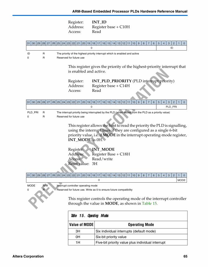
ARM-Based Embedded Processor PLDs Hardware Reference Manual
PRELIM
INARY IN
FORMAT
ION
Register: INT_IDAddress: Register base + C10HAccess: Read
This register gives the priority of the highest-priority interrupt that is enabled and active.
Register: INT_PLD_PRIORITY (PLD interrupt priority)Address: Register base + C14HAccess: Read
This register allows the host to read the priority the PLD is signalling, using the interrupt lines if they are configured as a single 6-bit priority value, i.e. if MODE in the interrupt operating-mode register, INT_MODE, is 0H.
Register: INT_MODEAddress: Register Base + C18HAccess: Read/writeReset value: 3H
This register controls the operating mode of the interrupt controller through the value in MODE, as shown in Table 15.
ID R The priority of the highest priority interrupt which is enabled and active
0 R Reserved for future use
12345678910111213141516171819202122232425262728293031 0
ID0
PLD_PRI R The interrupt priority being interrupted by the PLD (when routed from the PLD as a priority value)
0 R Reserved for future use
12345678910111213141516171819202122232425262728293031 0
PLD_PRI0
MODE R/W Interrupt controller operating mode
0 R Reserved for future use. Write as 0 to ensure future compatibility
12345678910111213141516171819202122232425262728293031 0
MODE0
Table 15. Operating Modes
Value of MODE Operating Mode
3H Six individual interrupts (default mode)
0H Six-bit priority value
1H Five-bit priority value plus individual interrupt
Altera Corporation 65
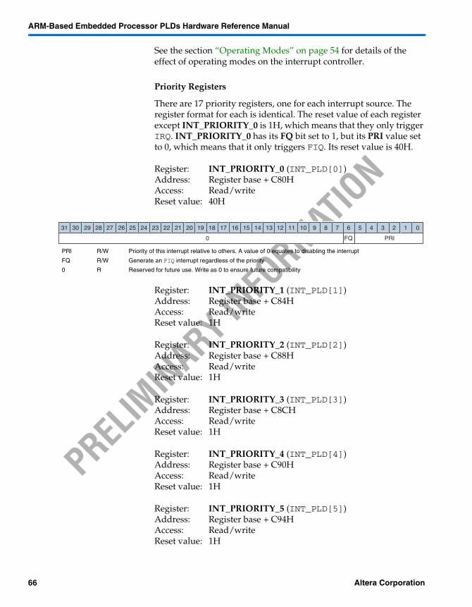
ARM-Based Embedded Processor PLDs Hardware Reference Manual
PRELIM
INARY IN
FORMAT
ION
See the section “Operating Modes” on page 54 for details of the effect of operating modes on the interrupt controller.
Priority Registers
There are 17 priority registers, one for each interrupt source. The register format for each is identical. The reset value of each register except INT_PRIORITY_0 is 1H, which means that they only trigger IRQ. INT_PRIORITY_0 has its FQ bit set to 1, but its PRI value set to 0, which means that it only triggers FIQ. Its reset value is 40H.
Register: INT_PRIORITY_0 (INT_PLD[0])Address: Register base + C80HAccess: Read/writeReset value: 40H
Register: INT_PRIORITY_1 (INT_PLD[1])Address: Register base + C84HAccess: Read/writeReset value: 1H
Register: INT_PRIORITY_2 (INT_PLD[2])Address: Register base + C88HAccess: Read/writeReset value: 1H
Register: INT_PRIORITY_3 (INT_PLD[3])Address: Register base + C8CHAccess: Read/writeReset value: 1H
Register: INT_PRIORITY_4 (INT_PLD[4])Address: Register base + C90HAccess: Read/writeReset value: 1H
Register: INT_PRIORITY_5 (INT_PLD[5])Address: Register base + C94HAccess: Read/writeReset value: 1H
PRI R/W Priority of this interrupt relative to others. A value of 0 equates to disabling the interrupt
FQ R/W Generate an FIQ interrupt regardless of the priority
0 R Reserved for future use. Write as 0 to ensure future compatibility
12345678910111213141516171819202122232425262728293031 0
PRI0 FQ
66 Altera Corporation
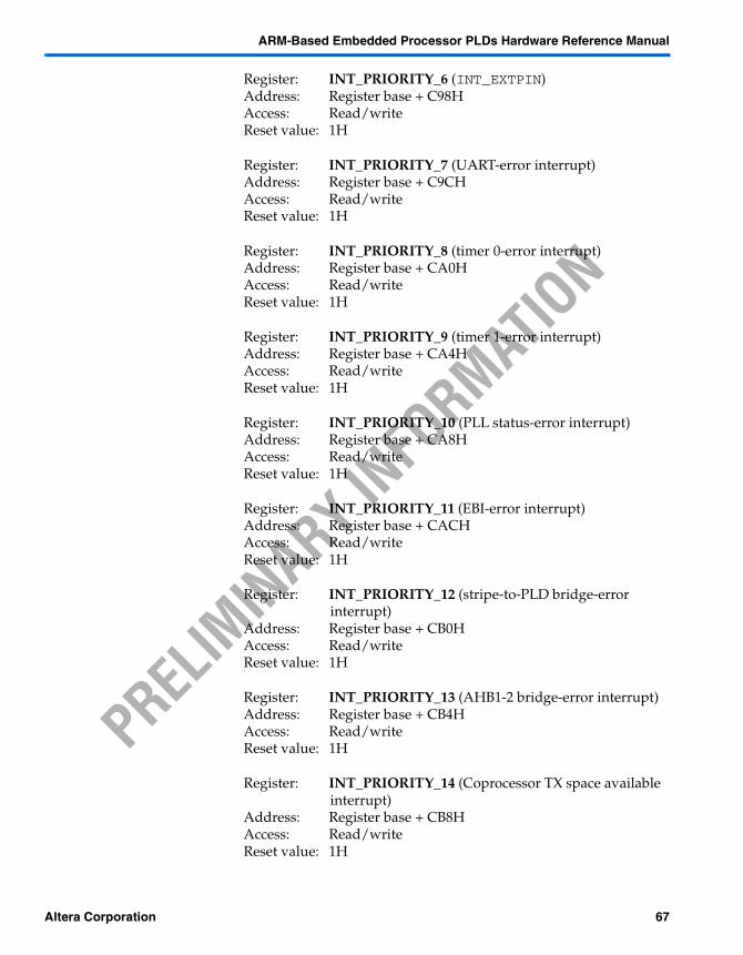
ARM-Based Embedded Processor PLDs Hardware Reference Manual
PRELIM
INARY IN
FORMAT
ION
Register: INT_PRIORITY_6 (INT_EXTPIN)Address: Register base + C98HAccess: Read/writeReset value: 1H
Register: INT_PRIORITY_7 (UART-error interrupt)Address: Register base + C9CHAccess: Read/writeReset value: 1H
Register: INT_PRIORITY_8 (timer 0-error interrupt)Address: Register base + CA0HAccess: Read/writeReset value: 1H
Register: INT_PRIORITY_9 (timer 1-error interrupt)Address: Register base + CA4HAccess: Read/writeReset value: 1H
Register: INT_PRIORITY_10 (PLL status-error interrupt)Address: Register base + CA8HAccess: Read/writeReset value: 1H
Register: INT_PRIORITY_11 (EBI-error interrupt)Address: Register base + CACHAccess: Read/writeReset value: 1H
Register: INT_PRIORITY_12 (stripe-to-PLD bridge-error interrupt)
Address: Register base + CB0HAccess: Read/writeReset value: 1H
Register: INT_PRIORITY_13 (AHB1-2 bridge-error interrupt)Address: Register base + CB4HAccess: Read/writeReset value: 1H
Register: INT_PRIORITY_14 (Coprocessor TX space available interrupt)
Address: Register base + CB8HAccess: Read/writeReset value: 1H
Altera Corporation 67
ARM-Based Embedded Processor PLDs Hardware Reference Manual
PRELIM
INARY IN
FORMAT
ION
Register: INT_PRIORITY_15 (Coprocessor RX data available interrupt)
Address: Register base + CBCHAccess: Read/writeReset value: 1H
Register: INT_PRIORITY_16 (Fastcomms RX data available interrupt)
Address: Register base + CC0HAccess: Read/writeReset value: 1H
Expansion Bus Interface
The expansion bus interface (EBI) is a 16-bit bidirectional external interface. The EBI provides a bridge between external devices, such as flash memories or memory-mapped devices, and the AHB bus. In addition, for slow external devices it provides for rate adaptation.
The memory controller runs synchronously to the AHB2 bus, supporting all transaction types, as defined in the AMBA Specification, Revision 2.0. The EBI manages data packing and unpacking automatically, based on endianness, block configuration and the size of the transaction selected by the master.
Figure 16 on page 63 shows the layout of the EBI.
68 Altera Corporation
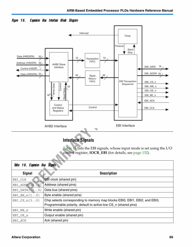
ARM-Based Embedded Processor PLDs Hardware Reference Manual
PRELIM
INARY IN
FORMAT
ION
Figure 16. Expansion Bus Interface Block Diagram
Interface Signals
Table 16 lists the EBI signals, whose input mode is set using the I/O control register, IOCR_EBI (for details, see page 132).
Data (HWDATA)
Control (HSIZE ... )
Data (HRDATA)
Timer
TransactionFIFO
ReadReturnFIFO
Controland StatusRegisters
AHB2 SlaveInterface
EBI TransactionSequencer
Address (HADDR)
32
32
32
72
32
72
32
AHB2 Interface
32 Writ
e D
ata
32
Res
d D
ata
EBI Interface
EBI_DATA
EBI_ADDR
16
25
EBI_CS_n
EBI_ACK
Interrupt
Start/Stop
Timeout
EBI_BE_n
EBI_OE_n
EBI_WE_n
EBI_CLK
Con
trol
Control
Table 16. Expansion Bus Signals
Signal Description
EBI_CLK EBI clock (shared pin)
EBI_ADDR[24..0] Address (shared pins)
EBI_DATA[15..0] Data bus (shared pins)
EBI_BE_n[1..0] Byte enable (shared pins)
EBI_CS_n[3..0] Chip selects corresponding to memory map blocks EBI0, EBI1, EBI2, and EBI3. Programmable polarity, default to active-low CS_n (shared pins)
EBI_WE_n Write enable (shared pin)
EBI_OE_n Output enable (shared pin)
EBI_ACK Ack (shared pin)
Altera Corporation 69
ARM-Based Embedded Processor PLDs Hardware Reference Manual
PRELIM
INARY IN
FORMAT
ION
EBI Operation
The EBI is extremely flexible, and can be configured to operate either synchronously or asynchronously. It can support four blocks of up to 32 Mbyte of external memory or memory-mapped devices of varying configurations. All blocks can be configured for 8- or 16-bit width. The base address and size of each block can be set in the memory map registers (see the section “Memory Map Control Registers” on page 10). In addition, users can monitor current activity using the EBI status register, EBI_SR.
In boot-from-flash mode, EBI0 width is selectable by configuration at power-up, because it is used in boot-from-flash mode. Additionally, in this mode, EBI0 is mapped at address 0 to allow booting from address 0, as required by the embedded processor.
The EBI is a slave-only interface, with a fixed programmable access period or asynchronous-acknowledge input selectable on a block-by-block basis. A clock can be output for synchronous operation, if required, with a programmable divide from the AHB2 clock frequency.
Splits
The EBI is capable of issuing a split response to AHB transactions that would otherwise tie up the bus for a long period, e.g., a long burst read from a slow 8-bit external device. This feature is disabled by default.
Do not enable split operation when peripherals with read side effects are connected to the EBI, because an undefined INCR transaction pre-fetches data from the EBI, which causes additional reads from the peripheral.
Switching Between Split and Non-Split Operation
The device can be switched from non-split (default) operation to split operation without difficulty. When switching from split to non-split operation, the user must ensure that the EBI transaction FIFO is empty, to provide a clean switch over. The EBI status register, EBI_SR, must be monitored, to check that a transaction is not in progress, so that a write to the control register, EBI_CR, can be performed in order to switch the split bit, SP.
70 Altera Corporation
ARM-Based Embedded Processor PLDs Hardware Reference Manual
PRELIM
INARY IN
FORMAT
ION
AHB Slave Interface
The AHB slave interface decodes bus transactions from an AHB bus master, and provides a suitable response to the appropriate block.
For control and status register read and write operations, the slave interface can operate at the full speed of the AHB2 clock and requires no wait-stating on the AHB bus. For writes or reads on the EBI, the slave interface posts a transaction to the transaction FIFO.
Write operations complete immediately, as far as the AHB bus is concerned. The status registers provide sufficient information to allow the EBI transaction sequencer to be monitored and operated safely.
For a non-split read, the slave interface stalls the AHB until the results of the read are available. However, this is the least-efficient type of read.
Split reads are supported, but to avoid the possibility of the system locking, no subsequent accesses are allowed, whether read or write, while a split read is outstanding. This is achieved by splitting the unwanted access without storing any data or control. The access completes at a later time, when the original split read has completed.
When splits are disabled (the default after a reset), a burst access results in the AHB bus being stalled for each word transaction. For a block configured as asynchronous, a timeout induces an error response on the AHB.
EBI Transaction Sequencer
The EBI transaction sequencer provides basic synchronous read and write cycles, which are shown in Figures 17 and 18 on page 66. It takes its input from the transaction FIFO output and uses this as an instruction, looking up the block number to obtain the key parameters for the sequence it subsequently performs. The block identifies an individually-programmable clock divide, which is used to control the speed of the sequence. The block also selects whether the sequence is synchronous, or depends on EBI_ACK to control completion.
Altera Corporation 71
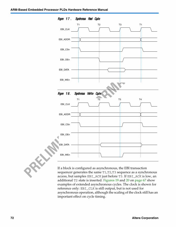
ARM-Based Embedded Processor PLDs Hardware Reference Manual
PRELIM
INARY IN
FORMAT
ION
Figure 17. Synchronous Read Cycle
Figure 18. Synchronous Write Cycle
If a block is configured as asynchronous, the EBI transaction sequencer generates the same T1,T2,T3 sequence as a synchronous access, but samples EBI_ACK just before T3. If EBI_ACK is low, an additional T2 state is inserted. Figures 19 and 20 on page 67 show examples of extended asynchronous cycles. The clock is shown for reference only: EBI_CLK is still output, but is not used for asynchronous operation, although the scaling of the clock still has an important effect on cycle timing.
EBI_CLK
EBI_ADDR
EBI_CSn
EBI_OEn
EBI_DATA
EBI_WEn
T1 T2 T3 T1
EBI_CLK
EBI_ADDR
EBI_CSn
EBI_OEn
EBI_DATA
EBI_WEn
T1 T2 T3 T4
72 Altera Corporation
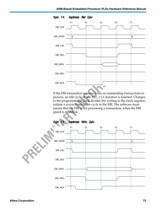
ARM-Based Embedded Processor PLDs Hardware Reference Manual
PRELIM
INARY IN
FORMAT
ION
Figure 19. Asynchronous Read Cycle
If the EBI transaction sequencer has no outstanding transactions to process, an idle cycle of one EBI_CLK duration is inserted. Changes to the programmable clock divider (by writing to the clock register) initiate a resynchronization cycle in the EBI. The software must ensure that the EBI is not processing a transaction, when the EBI speed is modified.
Figure 20. Asynchronous Write Cycle
EBI_CLK
EBI_ADDR
EBI_CSn
EBI_OEn
EBI_DATA
EBI_WEn
EBI_ACK
T1 T2 T3T2 T1
EBI_CLK
EBI_ADDR
EBI_CSn
EBI_OEn
EBI_DATA
EBI_WEn
EBI_ACK
T1 T2 T3T2 T1
Altera Corporation 73
ARM-Based Embedded Processor PLDs Hardware Reference Manual
PRELIM
INARY IN
FORMAT
ION
Where an asynchronous transaction is initiated and state T2 is reached, but EBI_ACK is not generated, the interface stalls in T2 until a timeout is generated. If timeouts are not used, this error could result in a system lock-up. The reset bit, R, in the EBI control register, EBI_CR, can be used to reset the module to an operational condition. For asynchronous read cycles, the data provided by the expansion device is clocked into the EBI by an AHB2 clock-synchronized rising ACK.
Read-Return FIFO
The read-return FIFO provides buffering for read transactions on the EBI. The transaction sequencer writes the data from the EBI into the read-return FIFO, along with information that allows the AHB slave interface to deliver the data to the correct AHB master. Multiple reads might be necessary to assemble a 32-bit word from two half-word transactions or from four byte transactions and deliver it to the read-return FIFO.
If splits are disabled, the read-return FIFO has a depth of one word. If splits are enabled, the read-return FIFO can fetch up to eight 32-bit values.
For split single-beat reads, the AHB slave posts the transaction into the transaction FIFO, and the EBI transaction sequencer performs the required number of reads to assemble and place the return value into the read-return FIFO. The AHB slave immediately completes the split.
For a fixed-beat burst, the initial NONSEQ AHB cycle is split, and the AHB slave posts a burst into the transaction FIFO. The EBI sequencer assembles and places the read values into the read-return FIFO. The transaction is unsplit when the required data has been read or the read-return FIFO is full. Bursts longer than eight words are split again when the master attempts to read the ninth word.
Byte and Word Mapping for Size and Endianness
Devices on the EBI can be 8- or 16-bits wide. Transactions on AHB2 can be 8-, 16-, or 32-bits wide. If the size of the AHB transaction is larger than the EBI device width, the transaction sequencer makes multiple EBI accesses. If the AHB transaction is smaller than the EBI, the transaction sequencer masks the data read or, if appropriate, uses byte enables.
74 Altera Corporation
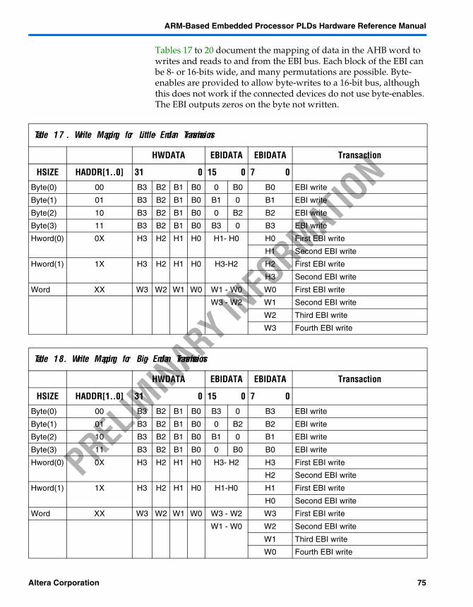
ARM-Based Embedded Processor PLDs Hardware Reference Manual
PRELIM
INARY IN
FORMAT
ION
Tables 17 to 20 document the mapping of data in the AHB word to writes and reads to and from the EBI bus. Each block of the EBI can be 8- or 16-bits wide, and many permutations are possible. Byte-enables are provided to allow byte-writes to a 16-bit bus, although this does not work if the connected devices do not use byte-enables. The EBI outputs zeros on the byte not written.
Table 17. Write Mapping for Little-Endian Transmissions
HWDATA EBIDATA EBIDATA Transaction
HSIZE HADDR[1..0] 31 0 15 0 7 0
Byte(0) 00 B3 B2 B1 B0 0 B0 B0 EBI write
Byte(1) 01 B3 B2 B1 B0 B1 0 B1 EBI write
Byte(2) 10 B3 B2 B1 B0 0 B2 B2 EBI write
Byte(3) 11 B3 B2 B1 B0 B3 0 B3 EBI write
Hword(0) 0X H3 H2 H1 H0 H1- H0 H0 First EBI write
H1 Second EBI write
Hword(1) 1X H3 H2 H1 H0 H3-H2 H2 First EBI write
H3 Second EBI write
Word XX W3 W2 W1 W0 W1 - W0 W0 First EBI write
W3 - W2 W1 Second EBI write
W2 Third EBI write
W3 Fourth EBI write
Table 18. Write Mapping for Big-Endian Transmissions
HWDATA EBIDATA EBIDATA Transaction
HSIZE HADDR[1..0] 31 0 15 0 7 0
Byte(0) 00 B3 B2 B1 B0 B3 0 B3 EBI write
Byte(1) 01 B3 B2 B1 B0 0 B2 B2 EBI write
Byte(2) 10 B3 B2 B1 B0 B1 0 B1 EBI write
Byte(3) 11 B3 B2 B1 B0 0 B0 B0 EBI write
Hword(0) 0X H3 H2 H1 H0 H3- H2 H3 First EBI write
H2 Second EBI write
Hword(1) 1X H3 H2 H1 H0 H1-H0 H1 First EBI write
H0 Second EBI write
Word XX W3 W2 W1 W0 W3 - W2 W3 First EBI write
W1 - W0 W2 Second EBI write
W1 Third EBI write
W0 Fourth EBI write
Altera Corporation 75
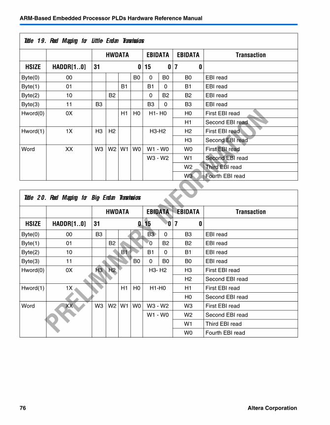
ARM-Based Embedded Processor PLDs Hardware Reference Manual
PRELIM
INARY IN
FORMAT
ION
Table 19. Read Mapping for Little-Endian Transmissions
HWDATA EBIDATA EBIDATA Transaction
HSIZE HADDR[1..0] 31 0 15 0 7 0
Byte(0) 00 B0 0 B0 B0 EBI read
Byte(1) 01 B1 B1 0 B1 EBI read
Byte(2) 10 B2 0 B2 B2 EBI read
Byte(3) 11 B3 B3 0 B3 EBI read
Hword(0) 0X H1 H0 H1- H0 H0 First EBI read
H1 Second EBI read
Hword(1) 1X H3 H2 H3-H2 H2 First EBI read
H3 Second EBI read
Word XX W3 W2 W1 W0 W1 - W0 W0 First EBI read
W3 - W2 W1 Second EBI read
W2 Third EBI read
W3 Fourth EBI read
Table 20. Read Mapping for Big-Endian Transmissions
HWDATA EBIDATA EBIDATA Transaction
HSIZE HADDR[1..0] 31 0 15 0 7 0
Byte(0) 00 B3 B3 0 B3 EBI read
Byte(1) 01 B2 0 B2 B2 EBI read
Byte(2) 10 B1 B1 0 B1 EBI read
Byte(3) 11 B0 0 B0 B0 EBI read
Hword(0) 0X H3 H2 H3- H2 H3 First EBI read
H2 Second EBI read
Hword(1) 1X H1 H0 H1-H0 H1 First EBI read
H0 Second EBI read
Word XX W3 W2 W1 W0 W3 - W2 W3 First EBI read
W1 - W0 W2 Second EBI read
W1 Third EBI read
W0 Fourth EBI read
76 Altera Corporation
ARM-Based Embedded Processor PLDs Hardware Reference Manual
PRELIM
INARY IN
FORMAT
ION
Timeout
A timeout on the EBI interface is the only source of interrupt. The address being accessed at the time of the interrupt is captured. Clearing the timeout interrupt re-enables the timeout function.
Clocking
The EBI_CLK is a simple division of the AHB2 clock. Although it is always used internally by the EBI transaction sequencer, the EBI_CLK output can be enabled or disabled as required by the application. The AHB2 clock and the EBI_CLK divider must be configured before enabling the EBI_CLK output, to avoid driving too high a frequency on it. Additionally, when booting from flash it is important to set the correct number of wait states for block 0 before reducing the EBI divide from its default value, to ensure that all accesses to the boot device are correctly timed.
Connecting External Devices to the EBI
The EBI can support up to four external devices of varying configurations. The following application notes explain how to connect the EBI to various off-chip peripherals.
Connecting the EBI of an ARM-Based Device to Flash Memory
Registers
Control and status registers are address-mapped and accessed by the system bus through the AHB slave-interface logic. Registers must be accessed with word-sized transactions, otherwise the EBI issues an ERROR response. EBI_CR, EBI_SR, EBI_INT_SR, and EBI_INT_ADDRSR relate to the whole EBI; registers EBI_BLOCK0 through EBI_BLOCK3 are for individual regions.
Unless otherwise stated, all register bits are zero after reset.
Altera Corporation 77
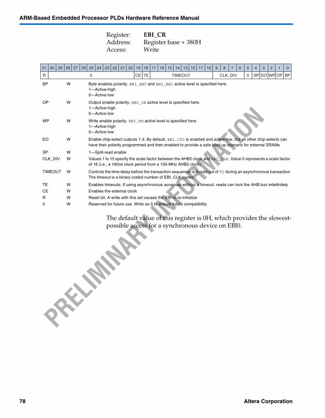
ARM-Based Embedded Processor PLDs Hardware Reference Manual
PRELIM
INARY IN
FORMAT
ION
Register: EBI_CRAddress: Register base + 380HAccess: Write
The default value of this register is 0H, which provides the slowest-possible access for a synchronous device on EBI0.
BP W Byte enables polarity. EBI_BE0 and EBI_BE1 active level is specified here.1—Active-high0—Active-low
OP W Output enable polarity. EBI_OE active level is specified here.1—Active-high0—Active-low
WP W Write enable polarity. EBI_WE active level is specified here.1—Active-high0—Active-low
EO W Enable chip-select outputs 1-3. By default, EBI_CS0 is enabled and active-low, but all other chip-selects can have their polarity programmed and then enabled to provide a safe boot-up scenario for external SRAMs
SP W 1—Split-read enable
CLK_DIV W Values 1 to 15 specify the scale factor between the AHB2 clock and EBI_CLK. Value 0 represents a scale factor of 16 (i.e., a 160ns clock period from a 100-MHz AHB2 clock)
TIMEOUT W Controls the time delay before the transaction sequencer is forced out of T2 during an asynchronous transaction The timeout is a binary-coded number of EBI_CLK cycles
TE W Enables timeouts. If using asynchronous accesses without a timeout, reads can lock the AHB bus indefinitely
CE W Enables the external clock
R W Reset bit. A write with this set causes the EBI to re-initialize
0 W Reserved for future use. Write as 0 to ensure future compatibility
12345678910111213141516171819202122232425262728293031 0
R CE TE TIMEOUT SPCLK_DIV EO WP OP BP0 0
78 Altera Corporation
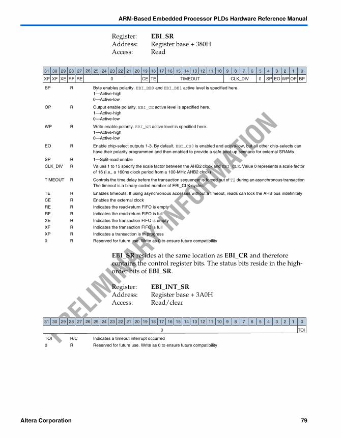
ARM-Based Embedded Processor PLDs Hardware Reference Manual
PRELIM
INARY IN
FORMAT
ION
Register: EBI_SRAddress: Register base + 380HAccess: Read
EBI_SR resides at the same location as EBI_CR and therefore contains the control register bits. The status bits reside in the high-order bits of EBI_SR.
Register: EBI_INT_SRAddress: Register base + 3A0HAccess: Read/clear
BP R Byte enables polarity. EBI_BE0 and EBI_BE1 active level is specified here.1—Active-high0—Active-low
OP R Output enable polarity. EBI_OE active level is specified here.1—Active-high0—Active-low
WP R Write enable polarity. EBI_WE active level is specified here.1—Active-high0—Active-low
EO R Enable chip-select outputs 1-3. By default, EBI_CS0 is enabled and active-low, but all other chip-selects can have their polarity programmed and then enabled to provide a safe boot-up scenario for external SRAMs
SP R 1—Split-read enable
CLK_DIV R Values 1 to 15 specify the scale factor between the AHB2 clock and EBI_CLK. Value 0 represents a scale factor of 16 (i.e., a 160ns clock period from a 100-MHz AHB2 clock)
TIMEOUT R Controls the time delay before the transaction sequencer is forced out of T2 during an asynchronous transaction The timeout is a binary-coded number of EBI_CLK cycles
TE R Enables timeouts. If using asynchronous accesses without a timeout, reads can lock the AHB bus indefinitely
CE R Enables the external clock
RE R Indicates the read-return FIFO is empty
RF R Indicates the read-return FIFO is full
XE R Indicates the transaction FIFO is empty
XF R Indicates the transaction FIFO is full
XP R Indicates a transaction is in progress
0 R Reserved for future use. Write as 0 to ensure future compatibility
12345678910111213141516171819202122232425262728293031 0
XP CE TE TIMEOUT SPCLK_DIV EO WP OP BP0 0XF XE RF RE
TOI R/C Indicates a timeout interrupt occurred
0 R Reserved for future use. Write as 0 to ensure future compatibility
12345678910111213141516171819202122232425262728293031 0
TOI0
Altera Corporation 79
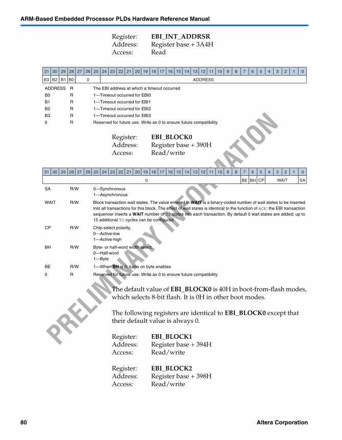
ARM-Based Embedded Processor PLDs Hardware Reference Manual
PRELIM
INARY IN
FORMAT
ION
Register: EBI_INT_ADDRSRAddress: Register base + 3A4HAccess: Read
Register: EBI_BLOCK0Address: Register base + 390HAccess: Read/write
The default value of EBI_BLOCK0 is 40H in boot-from-flash modes, which selects 8-bit flash. It is 0H in other boot modes.
The following registers are identical to EBI_BLOCK0 except that their default value is always 0.
Register: EBI_BLOCK1Address: Register base + 394HAccess: Read/write
Register: EBI_BLOCK2Address: Register base + 398HAccess: Read/write
ADDRESS R The EBI address at which a timeout occurred
B0 R 1—Timeout occurred for EBI0
B1 R 1—Timeout occurred for EBI1
B2 R 1—Timeout occurred for EBI2
B3 R 1—Timeout occurred for EBI3
0 R Reserved for future use. Write as 0 to ensure future compatibility
12345678910111213141516171819202122232425262728293031 0
ADDRESSB3 B2 B1 B0 0
SA R/W 0—Synchronous1—Asynchronous
WAIT R/W Block transaction wait states. The value entered in WAIT is a binary-coded number of wait states to be inserted into all transactions for this block. The effect of wait states is identical to the function of ACK: the EBI transaction sequencer inserts a WAIT number of T2 states into each transaction. By default 0 wait states are added; up to 15 additional T2 cycles can be configured
CP R/W Chip-select polarity.0—Active-low1—Active-high
BH R/W Byte- or half-word width select. 0—Half-word1—Byte
BE R/W 1—When BH is 0, turns on byte enables
0 R Reserved for future use. Write as 0 to ensure future compatibility
12345678910111213141516171819202122232425262728293031 0
BH CP WAIT SABE0
80 Altera Corporation
ARM-Based Embedded Processor PLDs Hardware Reference Manual
PRELIM
INARY IN
FORMAT
ION
Register: EBI_BLOCK3Address: Register base + 39CHAccess: Read/write
SDRAM Controller The SDRAM controller interfaces between the internal system buses and external synchronous DRAM. There are chip-selects for two blocks of devices, each of up to 256 Mbytes, giving support for a maximum of 512 Mbytes of memory. Up to eight banks are available, four per block, for optimized performance.
The SDRAM controller runs asynchronously to AHB1 and AHB2. It supports byte, half-word, and word transfers on the 32-bit system buses. Single beat, fixed-length incremental, fixed-length wrapping, and undefined-length incremental transfers are implemented. Early termination of a fixed-length transfer is accepted.
Either 16-bit or 32-bit SDR or DDR SDRAM (not both) can be connected, with clock speeds up to 133 MHz (SDR) or 266 MHz (DDR). The SDR interface supports Intel PC100/133-compatible SDRAM. The DDR interface is JEDEC-compliant, Intel-compliant PC200/266-compatible SDRAM.
Figure 21 on page 76 shows the SDRAM controller logic, and further sections detail the operation of each block.
Altera Corporation 81
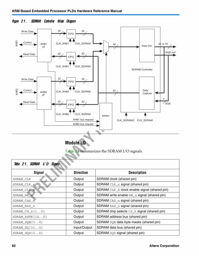
ARM-Based Embedded Processor PLDs Hardware Reference Manual
PRELIM
INARY IN
FORMAT
ION
Figure 21. SDRAM Controller Block Diagram
Module I/O
Table 21 summarizes the SDRAM I/O signals.
Write Data
Control
Read Data
AHB1I/F
FIFO
FIFO
32
32
CLK_SDRAMCLK_AHB1
CLK_SDRAM
Write Data
Control
Read Data
AHB2I/F
FIFO
FIFO
32
32
CLK_SDRAM
CLK_SDRAM
32
32
32
32
32Data Out
DataCapture
32
Arbiter
CLK_SDRAMCLK_SDRAM/2
SDRAM Controller
32 or 16
CLK_AHB1
CLK_AHB2
CLK_AHB2
DQS out*
4
DQS
AHB1 bus request
AHB2 bus request
AH
B1
AH
B2
Table 21. SDRAM I/O SIgnals
Signal Direction Description
SDRAM_CLK Output SDRAM clock (shared pin)
SDRAM_CLK_n Output SDRAM CLK_n signal (shared pin)
SDRAM_CLK_E Output SDRAM CLK_E clock enable signal (shared pin)
SDRAM_WE_n Output SDRAM write enable WE_n signal (shared pin)
SDRAM_CAS_n Output SDRAM CAS_n signal (shared pin)
SDRAM_RAS_n Output SDRAM RAS_n signal (shared pin)
SDRAM_CS_n[1..0] Output SDRAM chip selects CS_n signal (shared pin)
SDRAM_ADDR[14..0] Output SDRAM address bus (shared pin)
SDRAM_DQM[3..0] Output SDRAM DQM data byte masks (shared pin)
SDRAM_DQ[31..0] Input/Output SDRAM data bus (shared pin)
SDRAM_DQS[3..0] Output SDRAM DQS signal (shared pin)
82 Altera Corporation
ARM-Based Embedded Processor PLDs Hardware Reference Manual
PRELIM
INARY IN
FORMAT
ION
All external signals are capable of interfacing with signals of 3.3-V LVTTL or 2.5-V SSTL_2 class II (15.2 mA). The mode is determined using the IOCR_SDRAM register (see page 132), with LVTTL as the default. The operating voltage is determined by the supply provided.
Bus Interface
The bus interface logic accepts write and read operations for the external memory and local configuration registers.
The SDRAM controller is clocked by PLL2 and operates asynchronously to AHB1 and AHB2. The bus interface module contains synchronization circuitry to re-time data and control signals to the SDRAM controller.
Write operations are posted to an 8-word FIFO, and are usually acknowledged immediately. However, if the FIFO is full, the write operation is held in a wait state until the data can be accepted.
Read operations are held in a wait state while the SDRAM controller fetches the data.
All transfers within a burst must be aligned to the address boundary equal to the size of the transfer. Little-endian and big-endian data formats can be used, with the mode selected as required.
Endianness
Before changing big-endian and little-endian data formats, ensure that the SDRAM is idle.
Byte and Word Mapping for Size and Endianness
Devices on the SDRAM can be 32- or 16-bits wide. Transactions on AHB2 can be 8-, 16-, or 32-bits wide. If the size of the AHB transaction is larger than the SDRAM device width, the transaction sequencer makes multiple SDRAM accesses. If the AHB transaction is smaller than the SDRAM, the transaction sequencer masks the data read or, if appropriate, uses byte enables.
Tables 22 to 25 document the mapping of data in the AHB word to writes and reads to and from the SDRAM. Each block of the SDRAM can be 32- or 16-bits wide, and many permutations are possible. The SDRAM outputs zeros on any byte not written.
Altera Corporation 83
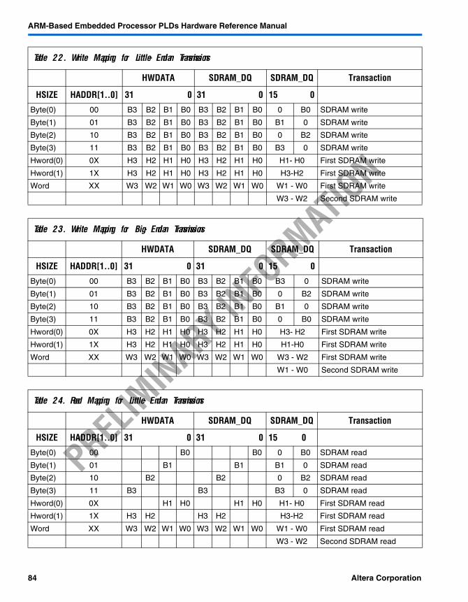
ARM-Based Embedded Processor PLDs Hardware Reference Manual
PRELIM
INARY IN
FORMAT
ION
Table 22. Write Mapping for Little-Endian Transmissions
HWDATA SDRAM_DQ SDRAM_DQ Transaction
HSIZE HADDR[1..0] 31 0 31 0 15 0
Byte(0) 00 B3 B2 B1 B0 B3 B2 B1 B0 0 B0 SDRAM write
Byte(1) 01 B3 B2 B1 B0 B3 B2 B1 B0 B1 0 SDRAM write
Byte(2) 10 B3 B2 B1 B0 B3 B2 B1 B0 0 B2 SDRAM write
Byte(3) 11 B3 B2 B1 B0 B3 B2 B1 B0 B3 0 SDRAM write
Hword(0) 0X H3 H2 H1 H0 H3 H2 H1 H0 H1- H0 First SDRAM write
Hword(1) 1X H3 H2 H1 H0 H3 H2 H1 H0 H3-H2 First SDRAM write
Word XX W3 W2 W1 W0 W3 W2 W1 W0 W1 - W0 First SDRAM write
W3 - W2 Second SDRAM write
Table 23. Write Mapping for Big-Endian Transmissions
HWDATA SDRAM_DQ SDRAM_DQ Transaction
HSIZE HADDR[1..0] 31 0 31 0 15 0
Byte(0) 00 B3 B2 B1 B0 B3 B2 B1 B0 B3 0 SDRAM write
Byte(1) 01 B3 B2 B1 B0 B3 B2 B1 B0 0 B2 SDRAM write
Byte(2) 10 B3 B2 B1 B0 B3 B2 B1 B0 B1 0 SDRAM write
Byte(3) 11 B3 B2 B1 B0 B3 B2 B1 B0 0 B0 SDRAM write
Hword(0) 0X H3 H2 H1 H0 H3 H2 H1 H0 H3- H2 First SDRAM write
Hword(1) 1X H3 H2 H1 H0 H3 H2 H1 H0 H1-H0 First SDRAM write
Word XX W3 W2 W1 W0 W3 W2 W1 W0 W3 - W2 First SDRAM write
W1 - W0 Second SDRAM write
Table 24. Read Mapping for Little-Endian Transmissions
HWDATA SDRAM_DQ SDRAM_DQ Transaction
HSIZE HADDR[1..0] 31 0 31 0 15 0
Byte(0) 00 B0 B0 0 B0 SDRAM read
Byte(1) 01 B1 B1 B1 0 SDRAM read
Byte(2) 10 B2 B2 0 B2 SDRAM read
Byte(3) 11 B3 B3 B3 0 SDRAM read
Hword(0) 0X H1 H0 H1 H0 H1- H0 First SDRAM read
Hword(1) 1X H3 H2 H3 H2 H3-H2 First SDRAM read
Word XX W3 W2 W1 W0 W3 W2 W1 W0 W1 - W0 First SDRAM read
W3 - W2 Second SDRAM read
84 Altera Corporation
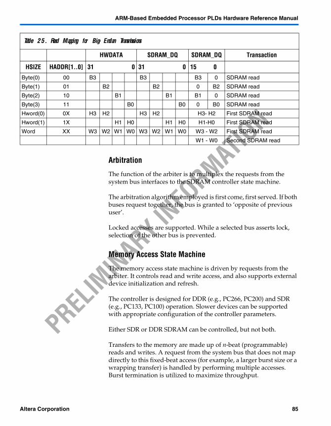
ARM-Based Embedded Processor PLDs Hardware Reference Manual
PRELIM
INARY IN
FORMAT
ION
Arbitration
The function of the arbiter is to multiplex the requests from the system bus interfaces to the SDRAM controller state machine.
The arbitration algorithm employed is first come, first served. If both buses request together, the bus is granted to ‘opposite of previous user’.
Locked accesses are supported. While a selected bus asserts lock, selection of the other bus is prevented.
Memory Access State Machine
The memory access state machine is driven by requests from the arbiter. It controls read and write access, and also supports external device initialization and refresh.
The controller is designed for DDR (e.g., PC266, PC200) and SDR (e.g., PC133, PC100) operation. Slower devices can be supported with appropriate configuration of the controller parameters.
Either SDR or DDR SDRAM can be controlled, but not both.
Transfers to the memory are made up of n-beat (programmable) reads and writes. A request from the system bus that does not map directly to this fixed-beat access (for example, a larger burst size or a wrapping transfer) is handled by performing multiple accesses. Burst termination is utilized to maximize throughput.
Table 25. Read Mapping for Big-Endian Transmissions
HWDATA SDRAM_DQ SDRAM_DQ Transaction
HSIZE HADDR[1..0] 31 0 31 0 15 0
Byte(0) 00 B3 B3 B3 0 SDRAM read
Byte(1) 01 B2 B2 0 B2 SDRAM read
Byte(2) 10 B1 B1 B1 0 SDRAM read
Byte(3) 11 B0 B0 0 B0 SDRAM read
Hword(0) 0X H3 H2 H3 H2 H3- H2 First SDRAM read
Hword(1) 1X H1 H0 H1 H0 H1-H0 First SDRAM read
Word XX W3 W2 W1 W0 W3 W2 W1 W0 W3 - W2 First SDRAM read
W1 - W0 Second SDRAM read
Altera Corporation 85
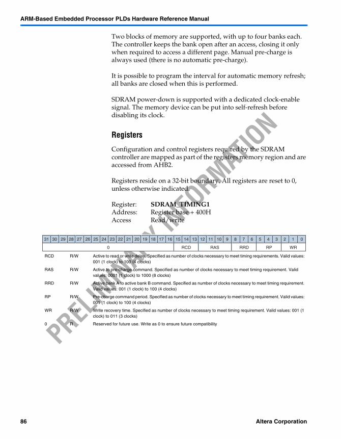
ARM-Based Embedded Processor PLDs Hardware Reference Manual
PRELIM
INARY IN
FORMAT
ION
Two blocks of memory are supported, with up to four banks each. The controller keeps the bank open after an access, closing it only when required to access a different page. Manual pre-charge is always used (there is no automatic pre-charge).
It is possible to program the interval for automatic memory refresh; all banks are closed when this is performed.
SDRAM power-down is supported with a dedicated clock-enable signal. The memory device can be put into self-refresh before disabling its clock.
Registers
Configuration and control registers required by the SDRAM controller are mapped as part of the registers memory region and are accessed from AHB2.
Registers reside on a 32-bit boundary. All registers are reset to 0, unless otherwise indicated.
Register: SDRAM_TIMING1Address: Register base + 400HAccess Read/write
RCD R/W Active to read or write delay. Specified as number of clocks necessary to meet timing requirements. Valid values: 001 (1 clock) to 100 (4 clocks)
RAS R/W Active to pre-charge command. Specified as number of clocks necessary to meet timing requirement. Valid values: 0001 (1 clock) to 1000 (8 clocks)
RRD R/W Active bank A to active bank B command. Specified as number of clocks necessary to meet timing requirement. Valid values: 001 (1 clock) to 100 (4 clocks)
RP R/W Pre-charge command period. Specified as number of clocks necessary to meet timing requirement. Valid values: 001 (1 clock) to 100 (4 clocks)
WR R/W Write recovery time. Specified as number of clocks necessary to meet timing requirement. Valid values: 001 (1 clock) to 011 (3 clocks)
0 R Reserved for future use. Write as 0 to ensure future compatibility
12345678910111213141516171819202122232425262728293031 0
WRRPRRDRASRCD0
86 Altera Corporation
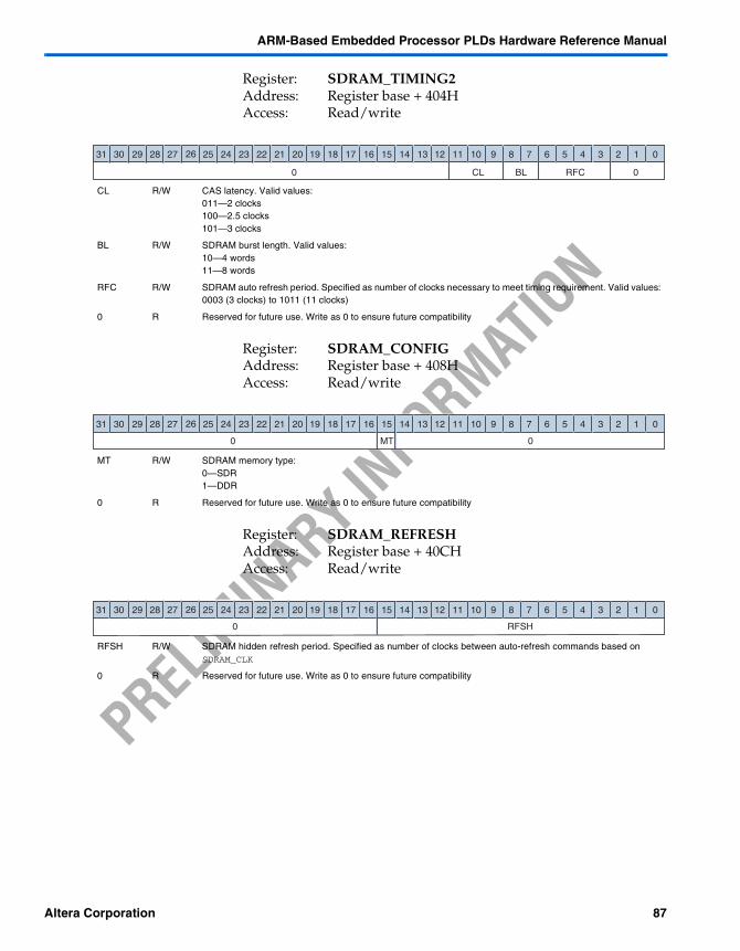
ARM-Based Embedded Processor PLDs Hardware Reference Manual
PRELIM
INARY IN
FORMAT
ION
Register: SDRAM_TIMING2Address: Register base + 404HAccess: Read/write
Register: SDRAM_CONFIGAddress: Register base + 408HAccess: Read/write
Register: SDRAM_REFRESHAddress: Register base + 40CHAccess: Read/write
CL R/W CAS latency. Valid values:011—2 clocks100—2.5 clocks101—3 clocks
BL R/W SDRAM burst length. Valid values:10—4 words11—8 words
RFC R/W SDRAM auto refresh period. Specified as number of clocks necessary to meet timing requirement. Valid values: 0003 (3 clocks) to 1011 (11 clocks)
0 R Reserved for future use. Write as 0 to ensure future compatibility
12345678910111213141516171819202122232425262728293031 0
0 CL BL RFC 0
MT R/W SDRAM memory type:0—SDR1—DDR
0 R Reserved for future use. Write as 0 to ensure future compatibility
12345678910111213141516171819202122232425262728293031 0
MT0 0
RFSH R/W SDRAM hidden refresh period. Specified as number of clocks between auto-refresh commands based on SDRAM_CLK
0 R Reserved for future use. Write as 0 to ensure future compatibility
12345678910111213141516171819202122232425262728293031 0
0 RFSH
Altera Corporation 87
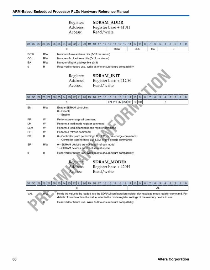
ARM-Based Embedded Processor PLDs Hardware Reference Manual
PRELIM
INARY IN
FORMAT
ION
Register: SDRAM_ADDRAddress: Register base + 410HAccess: Read/write
Register: SDRAM_INITAddress: Register base + 41CHAccess: Read/write
Register: SDRAM_MODE0Address: Register base + 420HAccess: Read/write
ROW R/W Number of row address bits (0-13 maximum)
COL R/W Number of col address bits (0-12 maximum)
BA R/W Number of bank address bits (0-3)
0 R Reserved for future use. Write as 0 to ensure future compatibility
12345678910111213141516171819202122232425262728293031 0
0 ROW COL BA 0
EN R/W Enable SDRAM controller:0—Disable1—Enable
PR W Perform pre-charge all command
LM W Perform a load mode register command
LEM W Perform a load extended mode register command
RF W Perform a refresh command
BS R 0—Controller is not performing LM, LEM, or pre-charge commands1—Controller is performing LM, LEM, or pre-charge commands
SR R/W 0—SDRAM devices are not in self-refresh mode1—SDRAM devices are in self-refresh mode
0 R Reserved for future use. Write as 0 to ensure future compatibility
12345678910111213141516171819202122232425262728293031 0
0 0EN PR LM LEM RF BS SR
VAL R/W Holds the value to be loaded into the SDRAM configuration register during a load mode register command. For details of how to obtain this value, refer to the mode register settings of the memory device in use
0 R Reserved for future use. Write as 0 to ensure future compatibility
12345678910111213141516171819202122232425262728293031 0
0 VAL
88 Altera Corporation
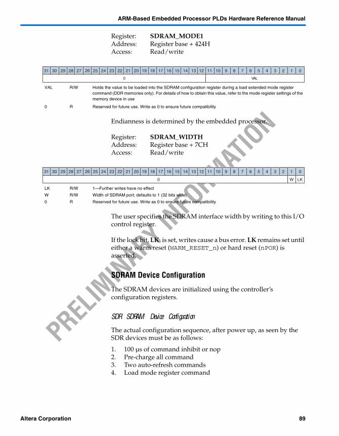
ARM-Based Embedded Processor PLDs Hardware Reference Manual
PRELIM
INARY IN
FORMAT
ION
Register: SDRAM_MODE1Address: Register base + 424HAccess: Read/write
Endianness is determined by the embedded processor.
Register: SDRAM_WIDTHAddress: Register base + 7CHAccess: Read/write
The user specifies the SDRAM interface width by writing to this I/O control register.
If the lock bit, LK, is set, writes cause a bus error. LK remains set until either a warm reset (WARM_RESET_n) or hard reset (nPOR) is asserted.
SDRAM Device Configuration
The SDRAM devices are initialized using the controller’s configuration registers.
SDR SDRAM Device Configuration
The actual configuration sequence, after power up, as seen by the SDR devices must be as follows:
1. 100 µs of command inhibit or nop2. Pre-charge all command3. Two auto-refresh commands4. Load mode register command
VAL R/W Holds the value to be loaded into the SDRAM configuration register during a load extended mode register command (DDR memories only). For details of how to obtain this value, refer to the mode register settings of the memory device in use
0 R Reserved for future use. Write as 0 to ensure future compatibility
12345678910111213141516171819202122232425262728293031 0
0 VAL
LK R/W 1—Further writes have no effect
W R/W Width of SDRAM port; defaults to 1 (32 bits wide)
0 R Reserved for future use. Write as 0 to ensure future compatibility
12345678910111213141516171819202122232425262728293031 0
0 W LK
Altera Corporation 89

ARM-Based Embedded Processor PLDs Hardware Reference Manual
PRELIM
INARY IN
FORMAT
ION
For this sequence, the following actions are required, using the controller’s configuration registers:
1. Ensure that the SDRAM PLL is locked at the operating frequency and wait 100 µs before continuing to step 2
2. Set all of the SDRAM controller's configuration registers
3. Enable the controller by setting the SDRAM enable bit, EN, of SDRAM_INIT
4. Issue a pre-charge all command by setting the perform pre-charge bit, PR, of SDRAM_INIT. The busy bit, BS, in SDRAM_INIT indicates when the pre-charge command has completed
5. Issue two refresh commands, initiating each by setting the perform refresh bit, RF, of SDRAM_INIT
6. Issue a load mode register command by setting the load mode register bit, LM, of SDRAM_INIT. The SDRAM's mode register is loaded with the value that has been programmed into SDRAM_MODE0. The busy bit, BS, indicates when the load command has completed
DDR SDRAM Device Configuration
The actual configuration sequence, after power up, as seen by the DDR devices, is as follows:
1. 200 µs of command inhibit or nop2. Pre-charge all command3. Load extended mode register command4. Load mode register to reset the internal delay-locked loop
(DLL)5. Pre-charge all command6. Two auto-refresh commands7. Load mode register command
To achieve this sequence, the following actions are required, using the controller's configuration registers:
1. Ensure that the SDRAM PLL is locked at the operating frequency and wait 200 µs before continuing to step 2
2. Set all of the SDRAM controller's configuration registers
3. Enable the controller by setting the SDRAM enable bit, EN, of SDRAM_INIT
90 Altera Corporation
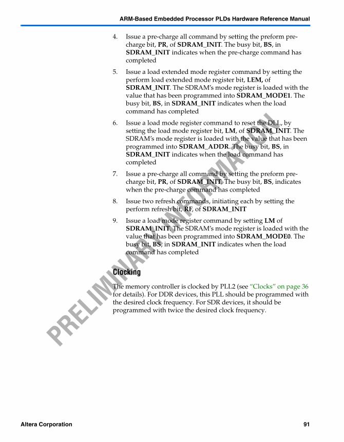
ARM-Based Embedded Processor PLDs Hardware Reference Manual
PRELIM
INARY IN
FORMAT
ION
4. Issue a pre-charge all command by setting the preform pre-charge bit, PR, of SDRAM_INIT. The busy bit, BS, in SDRAM_INIT indicates when the pre-charge command has completed
5. Issue a load extended mode register command by setting the perform load extended mode register bit, LEM, of SDRAM_INIT. The SDRAM’s mode register is loaded with the value that has been programmed into SDRAM_MODE1. The busy bit, BS, in SDRAM_INIT indicates when the load command has completed
6. Issue a load mode register command to reset the DLL, by setting the load mode register bit, LM, of SDRAM_INIT. The SDRAM’s mode register is loaded with the value that has been programmed into SDRAM_ADDR. The busy bit, BS, in SDRAM_INIT indicates when the load command has completed
7. Issue a pre-charge all command by setting the preform pre-charge bit, PR, of SDRAM_INIT. The busy bit, BS, indicates when the pre-charge command has completed
8. Issue two refresh commands, initiating each by setting the perform refresh bit, RF, of SDRAM_INIT
9. Issue a load mode register command by setting LM of SDRAM_INIT. The SDRAM’s mode register is loaded with the value that has been programmed into SDRAM_MODE0. The busy bit, BS, in SDRAM_INIT indicates when the load command has completed
Clocking
The memory controller is clocked by PLL2 (see “Clocks” on page 36 for details). For DDR devices, this PLL should be programmed with the desired clock frequency. For SDR devices, it should be programmed with twice the desired clock frequency.
Altera Corporation 91
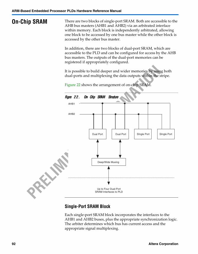
ARM-Based Embedded Processor PLDs Hardware Reference Manual
PRELIM
INARY IN
FORMAT
ION
On-Chip SRAM There are two blocks of single-port SRAM. Both are accessible to the AHB bus masters (AHB1 and AHB2) via an arbitrated interface within memory. Each block is independently arbitrated, allowing one block to be accessed by one bus master while the other block is accessed by the other bus master.
In addition, there are two blocks of dual-port SRAM, which are accessible to the PLD and can be configured for access by the AHB bus masters. The outputs of the dual-port memories can be registered if appropriately configured.
It is possible to build deeper and wider memories by using both dual-ports and multiplexing the data outputs within the stripe.
Figure 22 shows the arrangement of on-chip SRAM.
Figure 22. On-Chip SRAM Structure
Single-Port SRAM Block
Each single-port SRAM block incorporates the interfaces to the AHB1 and AHB2 buses, plus the appropriate synchronization logic. The arbiter determines which bus has current access and the appropriate signal multiplexing.
SIngle PortSIngle Port
AHB1
AHB2
Dual PortDual Port
Deep/Wide Muxing
Up to Four Dual-PortSRAM Interfaces to PLD
92 Altera Corporation
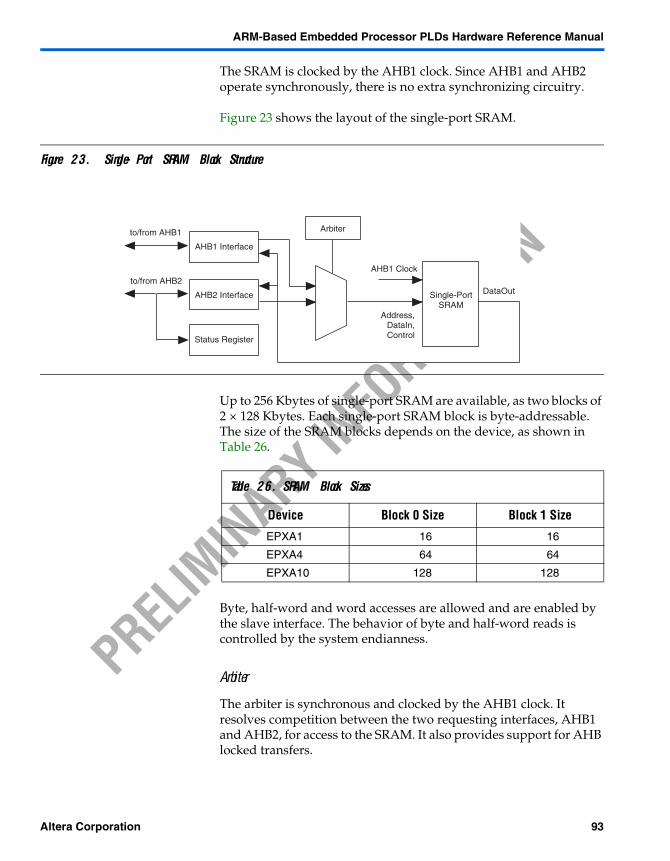
ARM-Based Embedded Processor PLDs Hardware Reference Manual
PRELIM
INARY IN
FORMAT
ION
The SRAM is clocked by the AHB1 clock. Since AHB1 and AHB2 operate synchronously, there is no extra synchronizing circuitry.
Figure 23 shows the layout of the single-port SRAM.
Figure 23. Single-Port SRAM Block Structure
Up to 256 Kbytes of single-port SRAM are available, as two blocks of 2 × 128 Kbytes. Each single-port SRAM block is byte-addressable. The size of the SRAM blocks depends on the device, as shown in Table 26.
Byte, half-word and word accesses are allowed and are enabled by the slave interface. The behavior of byte and half-word reads is controlled by the system endianness.
Arbiter
The arbiter is synchronous and clocked by the AHB1 clock. It resolves competition between the two requesting interfaces, AHB1 and AHB2, for access to the SRAM. It also provides support for AHB locked transfers.
Single-PortSRAM
AHB1 Clock
DataOut
Address,DataIn,Control
AHB1 Interface
AHB2 Interface
Status Register
to/from AHB1
to/from AHB2
Arbiter
Table 26. SRAM Block Sizes
Device Block 0 Size Block 1 Size
EPXA1 16 16
EPXA4 64 64
EPXA10 128 128
Altera Corporation 93
ARM-Based Embedded Processor PLDs Hardware Reference Manual
PRELIM
INARY IN
FORMAT
ION
The arbitration algorithm is a fixed round-robin scheme with fairness. This means that, if several masters are requesting access to the bus, the master least-recently granted is given access. Having granted a bus, the arbiter cannot rescind it but maintains the current grant until the appropriate request line has been de-asserted, indicating the end of a transfer. At this point the arbiter selects the next master to be granted access to the block.
Locked Transfers
Asserting a locking signal to the arbiter indicates that the requesting master requires back-to-back accesses for the duration of the assertion of the lock signal. Consequently, the arbiter maintains the grant until the locking signal is removed and the transfer has ended.
Bus Interfaces
When selected, the AHB1 interface provides a single-cycle response to transactions. An initial wait state can be inserted while the arbiter acknowledges the request for access to the SRAM. All AHB transaction types are supported.
The AHB2 interface synchronizes transfers between the AHB2 clock domain and the SRAM clock domain (AHB1). It provides a slave interface to the AHB2 buses, and outputs the required SRAM signals together with an interface to the arbiter.
Read Accesses
Read operations are held in a wait state while waiting for the arbiter and for the first cycle of the transfer. One word (or less) of data is returned in each subsequent cycle.
Write Accesses
Write operations are held in a wait state while waiting for the arbiter. One word (or less) of data is written in each subsequent cycle.
Registers
Register: SRAM0_SRAddress: Register base + 20HAccess: Read
This register has the same layout as SRAM1_SR on page 89.
94 Altera Corporation
ARM-Based Embedded Processor PLDs Hardware Reference Manual
PRELIM
INARY IN
FORMAT
ION
Register: SRAM1_SRAddress: Register base + 24HAccess: Read
SRAMx_SR contains the block size, in Kbytes, of the appropriate block of RAM.
Endianness
The single-port SRAM block supports little or big endian transfers as appropriate.
Dual-Port SRAM Block
Up to 128 Kbytes of dual-port SRAM are available, arranged as two 64-Kbyte blocks. Each block can be configured as two blocks, giving four in total; or alternatively the two blocks can be combined into one larger block. In addition, each block of dual-port SRAM can be configured independently of the other, giving many permutations of block configurations.
Each of the two blocks has the following characteristics:
It is byte-addressable from AHB interfaces It has a PLD interface capable of configuration to support
various widths and depths
When a block is split into two single-port RAMs. they both share the same clock.
The dual-port SRAM incorporates interfaces to the AHB1 and AHB2 buses, plus the appropriate synchronization logic. The arbiter determines which bus has current access and supplies the appropriate signal multiplexing.
Memory access from the PLD is synchronous and is triggered by the rising edge of the clock, as are input address, input data, write enable and chip enable. In read mode, data on the output bus is read from the memory location specified by the captured address.
Figure 24 on page 90 shows the layout of the dual-port SRAM.
SIZE R Memory block size in Kbytes (e.g. 32 Kbytes)
12345678910111213141516171819202122232425262728293031 0
SIZE
Altera Corporation 95
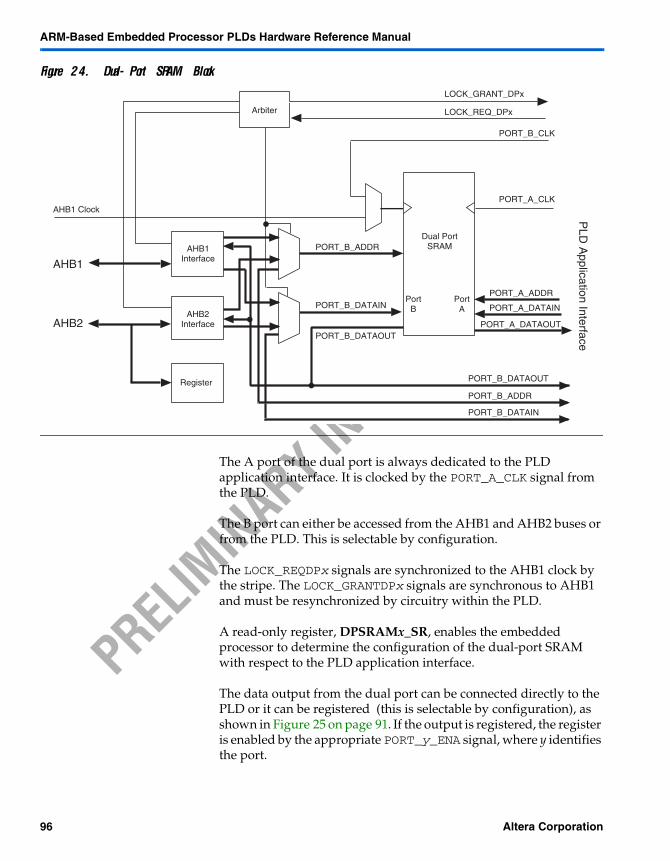
ARM-Based Embedded Processor PLDs Hardware Reference Manual
PRELIM
INARY IN
FORMAT
ION
Figure 24. Dual-Port SRAM Block
The A port of the dual port is always dedicated to the PLD application interface. It is clocked by the PORT_A_CLK signal from the PLD.
The B port can either be accessed from the AHB1 and AHB2 buses or from the PLD. This is selectable by configuration.
The LOCK_REQDPx signals are synchronized to the AHB1 clock by the stripe. The LOCK_GRANTDPx signals are synchronous to AHB1 and must be resynchronized by circuitry within the PLD.
A read-only register, DPSRAMx_SR, enables the embedded processor to determine the configuration of the dual-port SRAM with respect to the PLD application interface.
The data output from the dual port can be connected directly to the PLD or it can be registered (this is selectable by configuration), as shown in Figure 25 on page 91. If the output is registered, the register is enabled by the appropriate PORT_y_ENA signal, where y identifies the port.
Arbiter
AHB1 Clock
AHB1Interface
AHB2Interface
Register
AHB1
LOCK_REQ_DPx
PORT_B_CLK
PORT_A_CLK
Dual PortSRAM
PortB
PortA
PLD
Application Interface
LOCK_GRANT_DPx
PORT_B_ADDR
PORT_B_DATAIN
PORT_B_DATAOUT
PORT_A_ADDR
PORT_A_DATAIN
PORT_A_DATAOUTAHB2
PORT_B_DATAOUT
PORT_B_ADDR
PORT_B_DATAIN
96 Altera Corporation
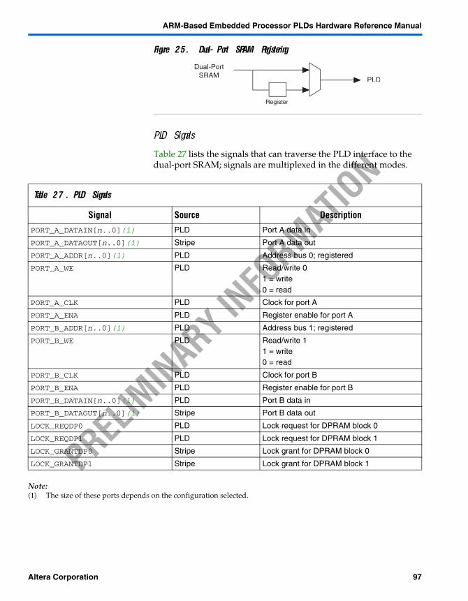
ARM-Based Embedded Processor PLDs Hardware Reference Manual
PRELIM
INARY IN
FORMAT
ION
Figure 25. Dual-Port SRAM Registering
PLD Signals
Table 27 lists the signals that can traverse the PLD interface to the dual-port SRAM; signals are multiplexed in the different modes.
Note:(1) The size of these ports depends on the configuration selected.
Register
Dual-PortSRAM
PLD
Table 27. PLD Signals
Signal Source Description
PORT_A_DATAIN[n..0](1) PLD Port A data in
PORT_A_DATAOUT[n..0](1) Stripe Port A data out
PORT_A_ADDR[n..0](1) PLD Address bus 0; registered
PORT_A_WE PLD Read/write 01 = write0 = read
PORT_A_CLK PLD Clock for port A
PORT_A_ENA PLD Register enable for port A
PORT_B_ADDR[n..0](1) PLD Address bus 1; registered
PORT_B_WE PLD Read/write 11 = write0 = read
PORT_B_CLK PLD Clock for port B
PORT_B_ENA PLD Register enable for port B
PORT_B_DATAIN[n..0](1) PLD Port B data in
PORT_B_DATAOUT[n..0](1) Stripe Port B data out
LOCK_REQDP0 PLD Lock request for DPRAM block 0
LOCK_REQDP1 PLD Lock request for DPRAM block 1
LOCK_GRANTDP0 Stripe Lock grant for DPRAM block 0
LOCK_GRANTDP1 Stripe Lock grant for DPRAM block 1
Altera Corporation 97
ARM-Based Embedded Processor PLDs Hardware Reference Manual
PRELIM
INARY IN
FORMAT
ION
Arbiter
The dual-port SRAM arbiter is the same as the single-port SRAM arbiter, but with additional lock control.
Dual-Port Locking
After the PLD has been configured, the dual port SRAMs can be accessed by the PLD at any time. Since they are true dual-port RAMs, the results of a read from one port which overlaps with a write to the same address from the other port are undefined. To prevent this, a locking mechanism is available, which prevents new accesses from AHB1 and AHB2 to the B port. The PLD can request that AHB1 and AHB2 be prevented from accessing the B port. Once the lock is granted, no new accesses are permitted from AHB1 and AHB2 to the lockable region within the appropriate DPSRAM block until the PLD releases the lock.
The PLD requests that AHB1 and AHB2 are locked out using the LOCK_REQDx signal. This signal is an input to the arbiter; it has the same priority as the AHB1 and AHB2 request signals. The LOCK_GRANTx signal indicates that the PLD has locked AHB1 and AHB2 from accessing the lockable region in the appropriate dual-port block (this signal is asynchronous to the PLD, so it must be re-timed to the appropriate clock within the PLD).
By default, the lockable region covers the whole of the dual-port block. This can be changed by modifying the contents of the DPSRAMx_LCR register.
The PLD can use the lock signals to perform safe read-modify-write accesses to the dual port.
Bus Interfaces
These interfaces are the same as for the single-port SRAM; however, if either interface is disabled, the interface provides a single-cycle ERROR response to any accesses.
Endianness
The dual-port SRAM block supports little- or big-endian transfers as appropriate.
98 Altera Corporation
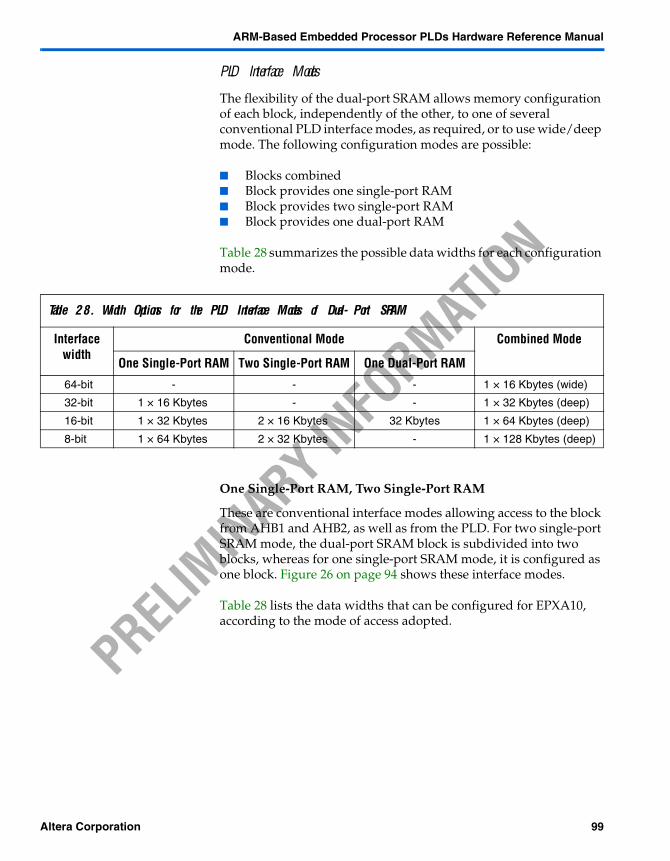
ARM-Based Embedded Processor PLDs Hardware Reference Manual
PRELIM
INARY IN
FORMAT
ION
PLD Interface Modes
The flexibility of the dual-port SRAM allows memory configuration of each block, independently of the other, to one of several conventional PLD interface modes, as required, or to use wide/deep mode. The following configuration modes are possible:
Blocks combined Block provides one single-port RAM Block provides two single-port RAM Block provides one dual-port RAM
Table 28 summarizes the possible data widths for each configuration mode.
One Single-Port RAM, Two Single-Port RAM
These are conventional interface modes allowing access to the block from AHB1 and AHB2, as well as from the PLD. For two single-port SRAM mode, the dual-port SRAM block is subdivided into two blocks, whereas for one single-port SRAM mode, it is configured as one block. Figure 26 on page 94 shows these interface modes.
Table 28 lists the data widths that can be configured for EPXA10, according to the mode of access adopted.
Table 28. Width Options for the PLD Interface Modes of Dual-Port SRAM
Interface width
Conventional Mode Combined Mode
One Single-Port RAM Two Single-Port RAM One Dual-Port RAM
64-bit - - - 1 × 16 Kbytes (wide)
32-bit 1 × 16 Kbytes - - 1 × 32 Kbytes (deep)
16-bit 1 × 32 Kbytes 2 × 16 Kbytes 32 Kbytes 1 × 64 Kbytes (deep)
8-bit 1 × 64 Kbytes 2 × 32 Kbytes - 1 × 128 Kbytes (deep)
Altera Corporation 99
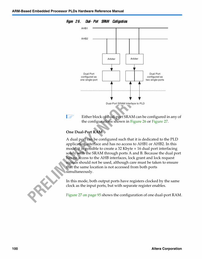
ARM-Based Embedded Processor PLDs Hardware Reference Manual
PRELIM
INARY IN
FORMAT
ION
Figure 26. Dual-Port SRAM Configurations
Either block of dual-port SRAM can be configured in any of the configurations shown in Figure 26 or Figure 27.
One Dual-Port RAM
A dual port can be configured such that it is dedicated to the PLD application interface and has no access to AHB1 or AHB2. In this mode, it is possible to create a 32 Kbyte × 16 dual port interfacing solely with the SRAM through ports A and B. Because the dual port has no access to the AHB interfaces, lock grant and lock request signals should not be used, although care must be taken to ensure that the same location is not accessed from both ports simultaneously.
In this mode, both output ports have registers clocked by the same clock as the input ports, but with separate register enables.
Figure 27 on page 95 shows the configuration of one dual-port RAM.
AHB1
AHB2
Dual Portconfigured as
two single-ports
Dual Portconfigured as
one single-port
Dual-Port SRAM Interface to PLD
Arbiter Arbiter
100 Altera Corporation
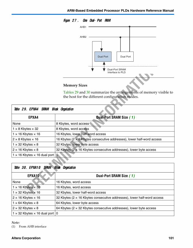
ARM-Based Embedded Processor PLDs Hardware Reference Manual
PRELIM
INARY IN
FORMAT
ION
Figure 27. One Dual-Port RAM
Memory Sizes
Tables 29 and 30 summarize the arrangements of memory visible to the host for the different configuration modes.
Note:(1) From AHB interface
AHB1
AHB2
Dual PortDual Port
Dual-Port SRAMInterface to PLD
Table 29. EPXA4 SRAM Block Organization
EPXA4 Dual-Port SRAM Size (1)
None 8 Kbytes, word access
1 × 8 Kbytes × 32 8 Kbytes, word access
1 × 16 Kbytes × 16 16 Kbytes, lower half-word access
2 × 8 Kbytes × 16 16 Kbytes (2 × 8 Kbytes consecutive addresses), lower half-word access
1 × 32 Kbytes × 8 32 Kbytes, lower byte access
2 × 16 Kbytes × 8 32 Kbytes (2 × 16 Kbytes consecutive addresses), lower byte access
1 × 16 Kbytes × 16 dual port 0
Table 30. EPXA10 SRAM Block Organization
EPXA10 Dual-Port SRAM Size (1)
None 16 Kbytes, word access
1 × 16 Kbytes × 32 16 Kbytes, word access
1 × 32 Kbytes × 16 32 Kbytes, lower half-word access
2 × 16 Kbytes × 16 32 Kbytes (2 × 16 Kbytes consecutive addresses), lower half-word access
1 × 64 Kbytes × 8 64 Kbytes, lower byte access
2 × 32 Kbytes × 8 64 Kbytes (2 × 32 Kbytes consecutive addresses), lower byte access
1 × 32 Kbytes × 16 dual port 0
Altera Corporation 101
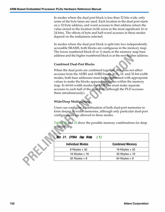
ARM-Based Embedded Processor PLDs Hardware Reference Manual
PRELIM
INARY IN
FORMAT
ION
In modes where the dual port block is less than 32 bits wide, only some of the byte lanes are used. Each location in the dual port starts on a 32-byte address, and word accesses to that address return the value stored in the location (with zeros in the most significant 16 or 24 bits). The effects of byte and half-word accesses in these modes depend on the endianness selected.
In modes where the dual port block is split into two independently accessible SRAMS, both blocks are contiguous in the memory map. The lower numbered block (0 or 1) starts at the memory map base address and the higher numbered block is at the next higher address.
Combined Dual-Port Blocks
When the dual ports are combined together, this does not affect accesses from the AHB1 and AHB2 buses. In 8-, 16- and 32-bit width modes, both base addresses must be programmed with appropriate values to make the blocks appear contiguous within the memory map. In 64-bit width modes the AHB bus must make separate accesses to each half of the dual port (although the PLD accesses them simultaneously).
Wide/Deep Multiplexing
Users can configure a combination of both dual-port memories to form deeper or wider memories, although only particular dual-port configurations are allowed in these modes.
Tables 31 and 32 show the possible memory combinations for deep multiplexing.
Table 31. EPXA4 Deep Modes (1)
Individual Modes Combined Memory
8 Kbytes × 32 16 Kbytes × 32
16 Kbytes × 16 32 Kbytes × 16
32 Kbytes × 8 64 Kbytes × 8
102 Altera Corporation
ARM-Based Embedded Processor PLDs Hardware Reference Manual
PRELIM
INARY IN
FORMAT
ION
Note:(1) The memories appear to the AHB interfaces as individual dual-port
memories (× 32, × 16, or × 8).
For EPXA10, wide mode is only applicable if both individual dual ports are configured as 16 Kbytes × 32, to give an overall memory of 16 Kbytes × 64. For EPXA4, the dual ports must be configured as 8 Kbytes × 32, to give an overall memory of 8 Kbytes × 64
Registers
The registers are all reset by WARM_RESET_n.
Register: DPSRAM0_SRAddress: Register base + 30HAccess: Read
The layout of this register is the same as for DPSRAM1_SR on page 97.
Register: DPSRAM1_SRAddress: Register base + 38HAccess: Read
Bits 31-12 of DPSRAMx_SR contain bits 31-12 of the block size, in Kbytes, for the appropriate block of RAM. Bits 11-0 of the block size are 0. The value held in SIZE does not change when MODE changes.
Table 32. EPXA10 Deep Modes (1)
Individual Modes Combined Memory
16 Kbytes × 32 32 Kbytes × 32
32 Kbytes × 16 64 Kbytes × 16
64 Kbytes × 8 128 Kbytes × 8
SIZE R Memory block size in bytes (e.g. 32 Kbytes)
GLBL R Global dual-port mode:00—Normal dual port01—Deep single port10—Wide single port
MODE R Mode[3]—Enables output registersMode[2..0]—Dual-port mode meanings depend on GLBL; see Table 33 for details.
0 R Reserved for future use. Write as 0 to ensure future compatibility
12345678910111213141516171819202122232425262728293031 0
SIZE 0 GLBL MODE
Altera Corporation 103
ARM-Based Embedded Processor PLDs Hardware Reference Manual
PRELIM
INARY IN
FORMAT
ION
Table 33 shows how the GLBL and MODE settings in DPSRAMx_SR affect dual-port SRAM configuration.
Address decoding for the dual-port registers occurs in the centralized AHB2 address decoder, which supplies the individual dual-port instances with the appropriate register select signals.
Register: DPSRAM0_LCRAddress: Register base + 34HAccess: Read/write
Register: DPSRAM1_LCRAddress: Register base + 3CHAccess: Read/write
For the appropriate block of dual-port SRAM, LOCK_REQDPx and LOCK_GRANTDPx signals cause AHB accesses to be locked from the address in LCKADDR. Accesses below these addresses are not affected by LOCK_REQDPx and LOCK_GRANTDPx.
Table 33. Dual-Port SRAM settings in DPSRAMx_SR
GLBL MODE[2..0] Dual Port Size and Mode
00 001 One single port 64Kbyte × 8
00 010 One single port 32Kbyte × 16
00 011 One single port 16Kbyte × 32
00 100 One dual port 32Kbyte × 16
00 101 Two single port 32Kbyte × 8
00 110 Two single port 16Kbyte × 16
01 001 One deep single port 64Kbyte × 8
01 010 One deep single port 32Kbyte × 16
01 011 One deep single port 16Kbyte × 32
10 011 One wide single port 8Kbyte × 64
LCKADDR R/W Bits [16..5] Start address (in blocks of 8 words) of the lock-addressable region. Default is 0, which means all of the RAM block is lockable
0 R Reserved for future use. Write as 0 to ensure future compatibility
12345678910111213141516171819202122232425262728293031 0
0 LCKADDR 0
104 Altera Corporation
ARM-Based Embedded Processor PLDs Hardware Reference Manual
PRELIM
INARY IN
FORMAT
ION
Reset and Mode Control
The ARM-based devices can be reset from many sources. The reset controller logic determines the cause of the reset, synchronizes it as necessary, and resets the appropriate logic blocks.
When any type of reset is asserted, the clock generator is placed in bypass mode, which automatically bypasses the PLLs and derives all clock outputs directly from the input reference.
Only a power-on reset initializes the embedded processor trace port, watchdog status, and configuration error status.
Types of Reset
There are various types of reset in the ARM-based devices, as follows:
Power-on reset Warm reset JTAG reset Configuration/reconfiguration Processor reset
These are explained in greater detail below.
Power-On Reset
There is one power-on reset signal for all clock domains, which resets only the following devices:
Embedded processor trace port Reset status register, RESET_SR (see page 105) Embedded JTAG controller
Warm Reset
There is one warm reset signal, for all clock domains, which results from all reset sources. It resets all embedded circuitry with the exception of the following devices:
Embedded processor trace port Reset status register, RESET_SR Embedded JTAG controller Part of the embedded configuration logic
A warm reset also asserts the external reset signal from the EBI, nRESET.
Altera Corporation 105
ARM-Based Embedded Processor PLDs Hardware Reference Manual
PRELIM
INARY IN
FORMAT
ION
Embedded JTAG
The JTAG input nTRST resets the JTAG controller in the PLD. Under certain conditions, it can also reset the JTAG controller in the embedded processor core, depending on the state of the external JSELECT pin. JSELECT determines whether PROC_nTRST or nTRST resets the JTAG controller in the embedded processor core.
Configuration/reconfiguration
A warm reset clears the contents of the PLD, in addition to re-booting the stripe. If BOOT_FLASH is 0, a warm reset also asserts nSTATUS to request reconfiguration.
Processor Reset
In boot-from-flash modes, the processor is held in reset for the duration of a warm reset.
In other modes, the processor is additionally held in reset while the configuration is loaded. It is released when the PLD enters user mode.
The BOOT_CR setting depends on external configuration pins; see page 104 for details.
Sources of Reset
Resets of the ARM-based devices can originate from several sources:
PLD power-on reset Resets from external sources
– Configuration pin nCONFIG– External reset pin nRESET (bidirectional open drain pin,
supplying reset output to configuration or flash devices)– External power-on reset nPOR
Resets from internal sources– Watchdog timer reset– JTAG module– Configuration error
These are explained below; “Reset Operation” on page 103 details the effects of these resets.
Figure 28 on page 101 shows the reset sequence for ARM-based devices.
106 Altera Corporation
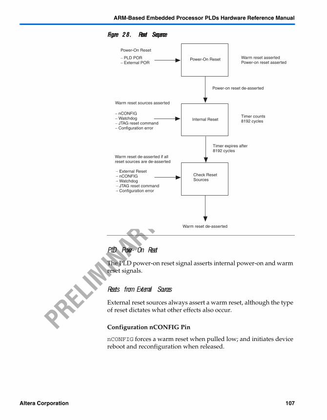
ARM-Based Embedded Processor PLDs Hardware Reference Manual
PRELIM
INARY IN
FORMAT
ION
Figure 28. Reset Sequence
PLD Power-On Reset
The PLD power-on reset signal asserts internal power-on and warm reset signals.
Resets from External Sources
External reset sources always assert a warm reset, although the type of reset dictates what other effects also occur.
Configuration nCONFIG Pin
nCONFIG forces a warm reset when pulled low; and initiates device reboot and reconfiguration when released.
Power-On Reset
Internal Reset
Check ResetSources
Power-On Reset
− PLD POR− External POR
Warm reset sources asserted
− nCONFIG− Watchdog− JTAG reset command− Configuration error
Warm reset de-asserted if all reset sources are de-asserted
− External Reset− nCONFIG− Watchdog− JTAG reset command− Configuration error
Warm reset assertedPower-on reset asserted
Power-on reset de-asserted
Timer counts8192 cycles
Timer expires after8192 cycles
Warm reset de-asserted
Altera Corporation 107
ARM-Based Embedded Processor PLDs Hardware Reference Manual
PRELIM
INARY IN
FORMAT
ION
External Reset Pin
The external reset pin nRESET is an active-low input that shares the pin with the reset output. It forces a warm reset when pulled low and must be asserted for sufficient time to reset any flash devices connected to the EBI. It does not start the reset counter. External de-bounce circuitry must be provided if the pin is to be connected to a mechanical reset switch.
External Power-On Reset Pin
The external power-on reset pin nPOR is active-low. When pulled low, it asserts both power-on and warm-reset signals.
Internal Sources of Reset
Internal reset sources always assert a warm reset, although the type of reset dictates what other effects also occur.
Software Watchdog Timer Reset
On reaching the programmed value, the software watchdog timer generates a trigger that invokes a warm reset.
JTAG
When the JTAG logic asserts a warm reset request, the reset module invokes a warm reset and holds the embedded processor in reset by setting the hold-microprocessor bit, HM, in the boot-control register, BOOT_CR.
Configuration Error
When the configuration logic detects a configuration error, the reset module invokes a warm reset under the following conditions:
External pin BOOT_FLASH is false The auto-reconfigure option in Quartus is set
108 Altera Corporation
ARM-Based Embedded Processor PLDs Hardware Reference Manual
PRELIM
INARY IN
FORMAT
ION
Reset Operation
Reset Counter
All reset events except assertion of the external reset pin trigger the reset counter, which controls the duration of the reset event and asserts a warm reset. Under certain conditions the reset counter also asserts an external reset output for a minimum of 51.2 µs, which is long enough to reset the external flash devices. When the reset counter reaches the reset assertion limit of 32768 clock cycles at the external clock frequency, the external reset output is negated, but warm reset remains asserted until all reset sources are negated.
Power On
At power on, the reset module asserts the external reset pin, nRESET, internal power-on and warm reset signals. The reset counter does not begin counting until the power-on signal is negated.
External Reset Input
Assertion of the external reset pin, nRESET, causes a warm reset. The reset counter begins counting as soon as the input is detected.
Reset Output
The reset output, nRESET, is active-low, open-drain and shares a pin with the external reset input. It is asserted during all reset events.
Warm Reset
When a warm reset source is asserted, except when it is triggered by an external reset, the reset output, nRESET, and warm reset are asserted, and the reset counter begins counting.
External Power-On Reset
Figures 29 and 30 on page 104 show the connectivity between the ARM-based family and a power supervisor. They also show how an external reset must be connected to flash memory.
Altera Corporation 109
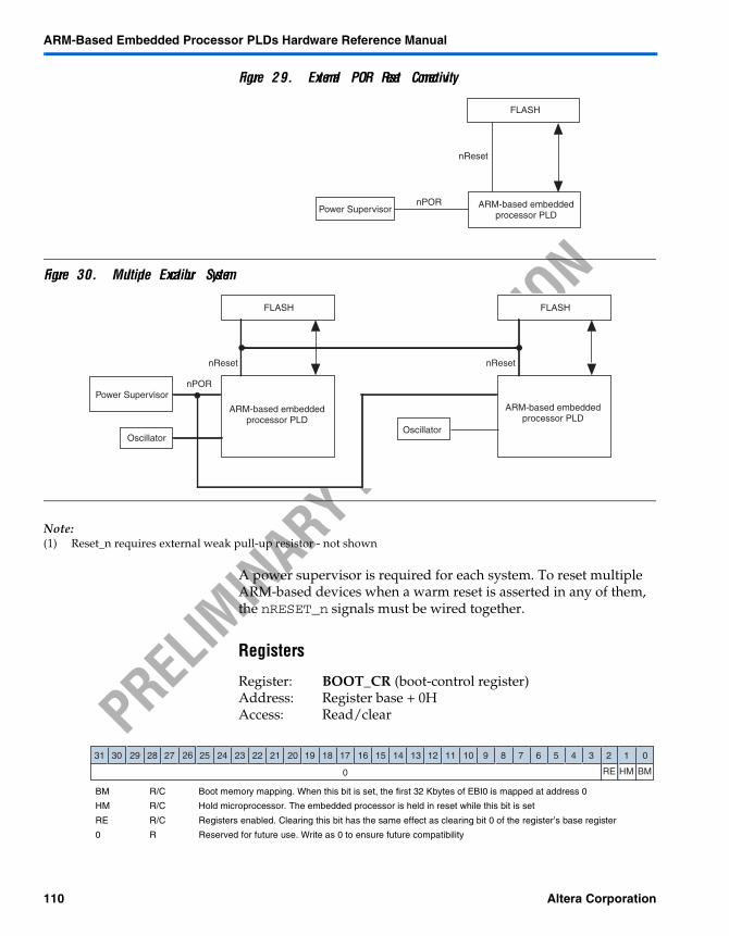
ARM-Based Embedded Processor PLDs Hardware Reference Manual
PRELIM
INARY IN
FORMAT
ION
Figure 29. External POR Reset Connectivity
Figure 30. Multiple Excalibur System
Note:(1) Reset_n requires external weak pull-up resistor - not shown
A power supervisor is required for each system. To reset multiple ARM-based devices when a warm reset is asserted in any of them, the nRESET_n signals must be wired together.
Registers
Register: BOOT_CR (boot-control register)Address: Register base + 0HAccess: Read/clear
nReset
FLASH
ARM-based embeddedprocessor PLD
Power SupervisornPOR
FLASH
ARM-based embeddedprocessor PLD
ARM-based embeddedprocessor PLD
Power Supervisor
OscillatorOscillator
nPOR
nReset nReset
FLASH
BM R/C Boot memory mapping. When this bit is set, the first 32 Kbytes of EBI0 is mapped at address 0
HM R/C Hold microprocessor. The embedded processor is held in reset while this bit is set
RE R/C Registers enabled. Clearing this bit has the same effect as clearing bit 0 of the register’s base register
0 R Reserved for future use. Write as 0 to ensure future compatibility
12345678910111213141516171819202122232425262728293031 0
RE HM BM0
110 Altera Corporation
ARM-Based Embedded Processor PLDs Hardware Reference Manual
PRELIM
INARY IN
FORMAT
ION
The reset value for this register depends on the configuration pins attached to the chip. In boot-from-flash modes, it has the value 7 if the reset source was the JTAG configuration-DMA scan chain, but otherwise it is 5. In other boot modes, it has the value 6, although the configuration bitstream usually resets HM.
Register: RESET_SR (reset status register)Address: Register base + 4HAccess: Read/clear
This register indicates the cause(s) of one or more previous reset events. nPOR clears it to 0H; other types of reset set the appropriate bit.
Register: IDCODE (identity and version register)Address: Register base + 8HAccess: Read
This register returns the value of the chip ID code, which is read from the device ID register within the embedded JTAG controller.
WR R/C Watchdog caused warm reset
CR R/C Configuration error caused warm reset
JT R/C JTAG caused warm reset
ER R/C External pin caused warm reset
0 R Reserved for future use. Write as 0 to ensure future compatibility
12345678910111213141516171819202122232425262728293031 0
JT CR WR0 ER
IDCODE R Chip ID code
12345678910111213141516171819202122232425262728293031 0
IDCODE
Altera Corporation 111
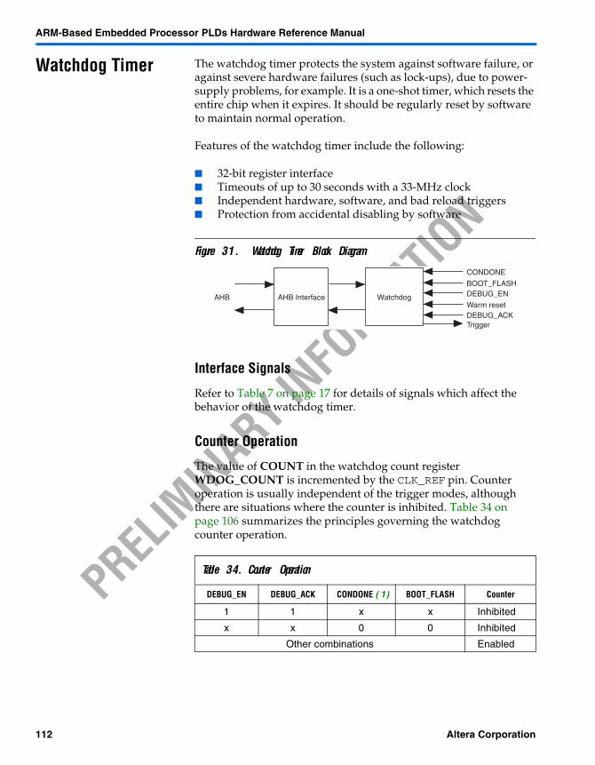
ARM-Based Embedded Processor PLDs Hardware Reference Manual
PRELIM
INARY IN
FORMAT
ION
Watchdog Timer The watchdog timer protects the system against software failure, or against severe hardware failures (such as lock-ups), due to power-supply problems, for example. It is a one-shot timer, which resets the entire chip when it expires. It should be regularly reset by software to maintain normal operation.
Features of the watchdog timer include the following:
32-bit register interface Timeouts of up to 30 seconds with a 33-MHz clock Independent hardware, software, and bad reload triggers Protection from accidental disabling by software
Figure 31. Watchdog Timer Block Diagram
Interface Signals
Refer to Table 7 on page 17 for details of signals which affect the behavior of the watchdog timer.
Counter Operation
The value of COUNT in the watchdog count register WDOG_COUNT is incremented by the CLK_REF pin. Counter operation is usually independent of the trigger modes, although there are situations where the counter is inhibited. Table 34 on page 106 summarizes the principles governing the watchdog counter operation.
Table 34. Counter Operation
DEBUG_EN DEBUG_ACK CONDONE (1) BOOT_FLASH Counter
1 1 x x Inhibited
x x 0 0 Inhibited
Other combinations Enabled
AHB WatchdogAHB Interface DEBUG_EN
Warm resetDEBUG_ACKTrigger
CONDONE
BOOT_FLASH
112 Altera Corporation

ARM-Based Embedded Processor PLDs Hardware Reference Manual
PRELIM
INARY IN
FORMAT
ION
Note:(1) CONDONE is a pin that, when low, signifies that the PLD is undergoing
configuration via the external port. When high, configuration is complete
DEBUG_ACK synchronization to CLK_REF results in a maximum delay of two CLK_REF periods between DEBUG_ACK assertion or de-assertion and the counter being inhibited or enabled.
Trigger Modes
When the watchdog triggers, it asserts a trigger that causes resets of all modules except for the trace logic, and provides a reset signal to external devices. (If the boot source is not flash memory, the watchdog reset causes a new code download.)
The watchdog timer can be triggered by the following events:
Hardware triggers Software triggers An unexpected value written to the reload register
The triggers operate independently of each other, and are described in detail below.
Hardware Trigger
A low value on the DEBUG_EN pin enables the hardware watchdog, which then triggers if COUNT in WDOG_COUNT overflows. The time represented by COUNT depends on the input frequency.
Software Trigger
Setting TRIGGER in WDOG_CR to a non-zero value enables the software trigger. When COUNT equals the trigger value from TRIGGER, the watchdog is triggered.
Bad Reload Value Trigger
The watchdog triggers if an unexpected value is written to WDOG_RELOAD. This process is explained more fully in ”Reloading the Watchdog Timer” below.
Reloading the Watchdog Timer
Two magic values can be written to WDOG_RELOAD:
Altera Corporation 113
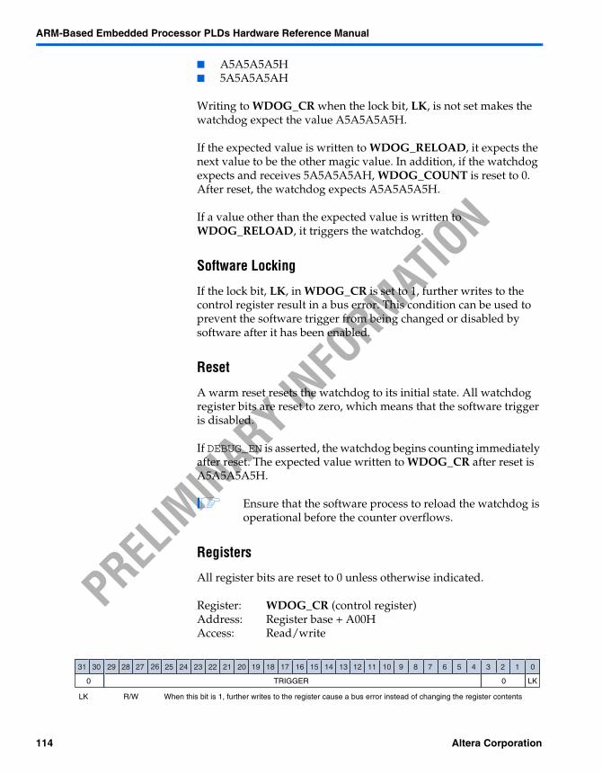
ARM-Based Embedded Processor PLDs Hardware Reference Manual
PRELIM
INARY IN
FORMAT
ION
A5A5A5A5H 5A5A5A5AH
Writing to WDOG_CR when the lock bit, LK, is not set makes the watchdog expect the value A5A5A5A5H.
If the expected value is written to WDOG_RELOAD, it expects the next value to be the other magic value. In addition, if the watchdog expects and receives 5A5A5A5AH, WDOG_COUNT is reset to 0. After reset, the watchdog expects A5A5A5A5H.
If a value other than the expected value is written to WDOG_RELOAD, it triggers the watchdog.
Software Locking
If the lock bit, LK, in WDOG_CR is set to 1, further writes to the control register result in a bus error. This condition can be used to prevent the software trigger from being changed or disabled by software after it has been enabled.
Reset
A warm reset resets the watchdog to its initial state. All watchdog register bits are reset to zero, which means that the software trigger is disabled.
If DEBUG_EN is asserted, the watchdog begins counting immediately after reset. The expected value written to WDOG_CR after reset is A5A5A5A5H.
Ensure that the software process to reload the watchdog is operational before the counter overflows.
Registers
All register bits are reset to 0 unless otherwise indicated.
Register: WDOG_CR (control register)Address: Register base + A00HAccess: Read/write
LK R/W When this bit is 1, further writes to the register cause a bus error instead of changing the register contents
12345678910111213141516171819202122232425262728293031 0
0 TRIGGER 0 LK
114 Altera Corporation
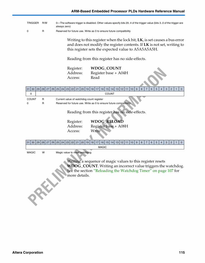
ARM-Based Embedded Processor PLDs Hardware Reference Manual
PRELIM
INARY IN
FORMAT
ION
Writing to this register when the lock bit, LK, is set causes a bus error and does not modify the register contents. If LK is not set, writing to this register sets the expected value to A5A5A5A5H.
Reading from this register has no side-effects.
Register: WDOG_COUNTAddress: Register base + A04HAccess: Read
Reading from this register has no side-effects.
Register: WDOG_RELOADAddress: Register base + A08HAccess: Write
Writing a sequence of magic values to this register resets WDOG_COUNT. Writing an incorrect value triggers the watchdog. See the section “Reloading the Watchdog Timer” on page 107 for more details.
TRIGGER R/W 0—The software trigger is disabled. Other values specify bits 29..4 of the trigger value (bits 3..0 of the trigger are always zero)
0 R Reserved for future use. Write as 0 to ensure future compatibility
COUNT R Current value of watchdog count register
0 R Reserved for future use. Write as 0 to ensure future compatibility
12345678910111213141516171819202122232425262728293031 0
0 COUNT
MAGIC W Magic value to reset watchdog
12345678910111213141516171819202122232425262728293031 0
MAGIC
Altera Corporation 115
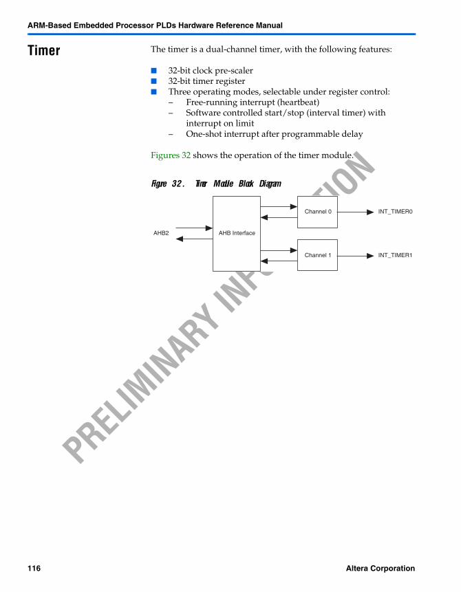
ARM-Based Embedded Processor PLDs Hardware Reference Manual
PRELIM
INARY IN
FORMAT
ION
Timer The timer is a dual-channel timer, with the following features:
32-bit clock pre-scaler 32-bit timer register Three operating modes, selectable under register control:
– Free-running interrupt (heartbeat)– Software controlled start/stop (interval timer) with
interrupt on limit– One-shot interrupt after programmable delay
Figures 32 shows the operation of the timer module.
Figure 32. Timer Module Block Diagram
AHB2 AHB Interface
Channel 1 INT_TIMER1
Channel 0 INT_TIMER0
116 Altera Corporation
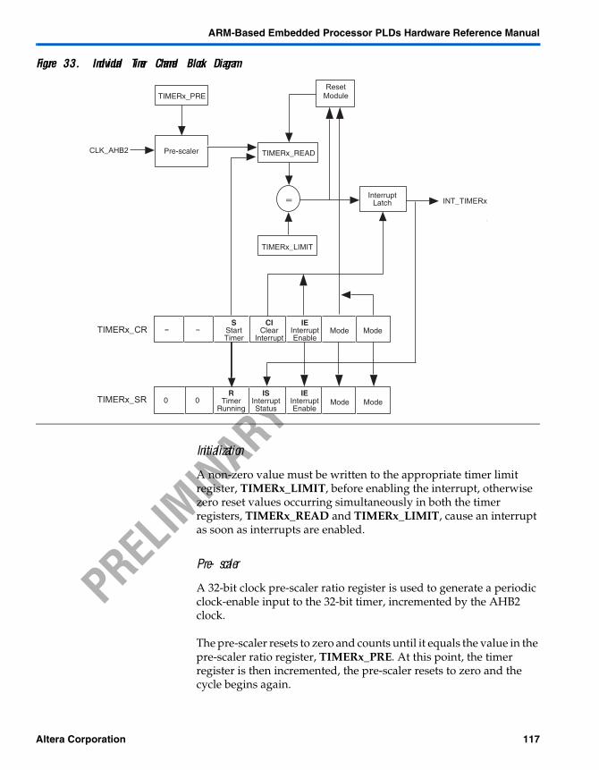
ARM-Based Embedded Processor PLDs Hardware Reference Manual
PRELIM
INARY IN
FORMAT
ION
Figure 33. Individual Timer Channel Block Diagram
Initialization
A non-zero value must be written to the appropriate timer limit register, TIMERx_LIMIT, before enabling the interrupt, otherwise zero reset values occurring simultaneously in both the timer registers, TIMERx_READ and TIMERx_LIMIT, cause an interrupt as soon as interrupts are enabled.
Pre-scaler
A 32-bit clock pre-scaler ratio register is used to generate a periodic clock-enable input to the 32-bit timer, incremented by the AHB2 clock.
The pre-scaler resets to zero and counts until it equals the value in the pre-scaler ratio register, TIMERx_PRE. At this point, the timer register is then incremented, the pre-scaler resets to zero and the cycle begins again.
ResetModule
Mode
Mode
Mode
ModeIE
InterruptEnable
IEInterruptEnable
CIClear
Interrupt
ISInterruptStatus
SStartTimer
RTimer
Running
- -
0 0
TIMERx_PRE
Pre-scaler TIMERx_READ
= INT_TIMERx
TIMERx_LIMIT
CLK_AHB2
TIMERx_CR
TIMERx_SR
InterruptLatch
Altera Corporation 117
ARM-Based Embedded Processor PLDs Hardware Reference Manual
PRELIM
INARY IN
FORMAT
ION
A value of zero in the pre-scaler ratio register permanently asserts the clock-enable to the timer register, resulting in the timer incrementing at the AHB2 clock rate.
Free-Running Heartbeat Mode
In free-running mode, the timer is reset to 0 when the start bit, S, in TIMERx_CR changes from 0 to 1. The timer then increments until it reaches the value LIMIT in TIMERx_LIMIT, at which point it is reset to 0 and begins incrementing again. This cycle repeats while S remains set. An interrupt is requested (if enabled) at the end of each cycle.
One-Shot Delay Mode
In one-shot mode, the timer is reset to 0 when the start bit, S, in TIMERx_CR changes from 0 to 1. The timer then increments until it reaches the value LIMIT in TIMERx_LIMIT, at which point the timer stops, S is cleared, and an interrupt is requested (if enabled). No further activity takes place.
Software Interval Timer Mode
In interval timer mode, the timer is reset to 0 when the start bit, S, in TIMERx_CR changes from 0 to 1. The timer then increments until S is cleared, at which point the timer is frozen. An interrupt is requested (if enabled) when the timer passes through the value LIMIT in TIMERx_LIMIT. If the timer value reaches FFFFFFFFH, it wraps around to 0 and continues incrementing.
Interrupts
When asserted, interrupts remain asserted until explicitly cleared by setting the clear-interrupt bit, CI, in TIMERx_CR, or until the timer module is reset by WARM_RESET_n. This corresponds to a level-sensitive interrupt scheme.
Software should use a read-modify-write sequence to set CI but preserve all other bits in TIMERx_CR.
Registers
Each timer channel has an identical register set. Suffixes 0 and 1 refer to channels 0 and 1 respectively. At reset, all internal registers, including interrupt outputs, are cleared.
118 Altera Corporation
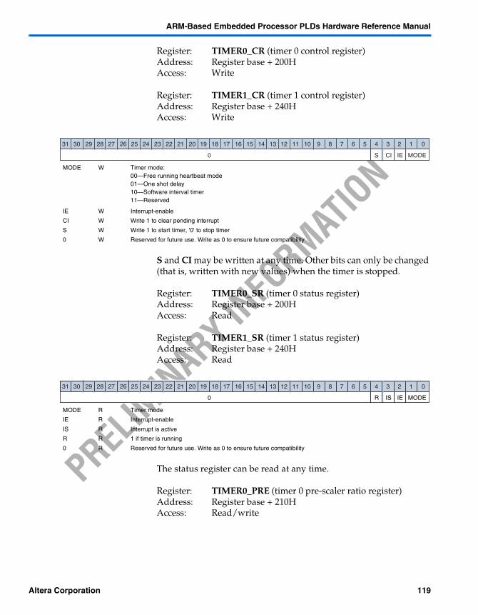
ARM-Based Embedded Processor PLDs Hardware Reference Manual
PRELIM
INARY IN
FORMAT
ION
Register: TIMER0_CR (timer 0 control register)Address: Register base + 200HAccess: Write
Register: TIMER1_CR (timer 1 control register)Address: Register base + 240HAccess: Write
S and CI may be written at any time. Other bits can only be changed (that is, written with new values) when the timer is stopped.
Register: TIMER0_SR (timer 0 status register)Address: Register base + 200HAccess: Read
Register: TIMER1_SR (timer 1 status register)Address: Register base + 240HAccess: Read
The status register can be read at any time.
Register: TIMER0_PRE (timer 0 pre-scaler ratio register)Address: Register base + 210HAccess: Read/write
MODE W Timer mode:00—Free running heartbeat mode01—One shot delay10—Software interval timer11—Reserved
IE W Interrupt-enable
CI W Write 1 to clear pending interrupt
S W Write 1 to start timer, '0' to stop timer
0 W Reserved for future use. Write as 0 to ensure future compatibility
12345678910111213141516171819202122232425262728293031 0
MODEIECIS0
MODE R Timer mode
IE R Interrupt-enable
IS R Interrupt is active
R R 1 if timer is running
0 R Reserved for future use. Write as 0 to ensure future compatibility
12345678910111213141516171819202122232425262728293031 0
MODEIEISR0
Altera Corporation 119
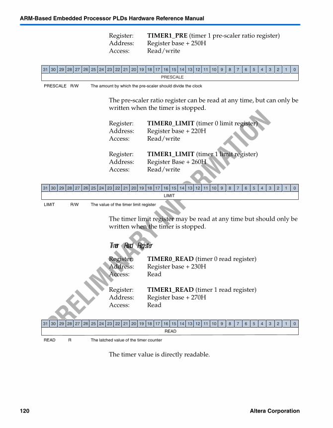
ARM-Based Embedded Processor PLDs Hardware Reference Manual
PRELIM
INARY IN
FORMAT
ION
Register: TIMER1_PRE (timer 1 pre-scaler ratio register)Address: Register base + 250HAccess: Read/write
The pre-scaler ratio register can be read at any time, but can only be written when the timer is stopped.
Register: TIMER0_LIMIT (timer 0 limit register)Address: Register base + 220HAccess: Read/write
Register: TIMER1_LIMIT (timer 1 limit register)Address: Register Base + 260HAccess: Read/write
The timer limit register may be read at any time but should only be written when the timer is stopped.
Timer Read Register
Register: TIMER0_READ (timer 0 read register)Address: Register base + 230HAccess: Read
Register: TIMER1_READ (timer 1 read register)Address: Register base + 270HAccess: Read
The timer value is directly readable.
PRESCALE R/W The amount by which the pre-scaler should divide the clock
12345678910111213141516171819202122232425262728293031 0
PRESCALE
LIMIT R/W The value of the timer limit register
12345678910111213141516171819202122232425262728293031 0
LIMIT
READ R The latched value of the timer counter
12345678910111213141516171819202122232425262728293031 0
READ
120 Altera Corporation
ARM-Based Embedded Processor PLDs Hardware Reference Manual
PRELIM
INARY IN
FORMAT
ION
UART The universal asynchronous receiver transmitter module (UART) performs serial-to-parallel conversion on data characters received from a peripheral device or modem, and parallel-to-serial conversion on data characters received from the embedded processor. The UART operates in FIFO mode, with the FIFOs having a depth of 16 bytes. The CPU can read the status of the UART at any time during operation. The UART reports status information, including the type and condition of the transfer being performed, and any error conditions.
The UART has the following features:
5 to 8 data bits 1 or 2 stop bits Even, odd, stick, or no parity 75 to 230,400 baud rate 16-byte transmit FIFO 16-byte receive FIFO. Programmable baud generator divides any input clock by 2 to
65535 and generates the 16 × baud clock Transmit FIFO interrupt for empty indication and transmitter
idle indication False-start bit detection Internal diagnostic capabilities
– Loop-back control for communications-link fault isolation– Break insertion and detection in loop-back mode
Modem communication support
Figure 34 on page 116 shows the layout of the UART.
Altera Corporation 121
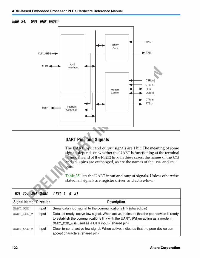
ARM-Based Embedded Processor PLDs Hardware Reference Manual
PRELIM
INARY IN
FORMAT
ION
Figure 34. UART Block Diagram
UART Pins and Signals
The UART input and output signals are 1 bit. The meaning of some signals depends on whether the UART is functioning at the terminal or modem end of the RS232 link. In these cases, the names of the RTS and CTS pins are exchanged, as are the names of the DSR and DTR pins.
Table 35 lists the UART input and output signals. Unless otherwise stated, all signals are register driven and active-low.
RXD
DSR_n
CTS_n
RI_n
DCD_n
DTR_n
RTS_n
TXD
AHB2AHB
Interface
UARTCore
ModemControl
InterruptController
INTR
CLK_AHB2
Table 35. UART Signals (Part 1 of 2)
Signal Name Direction Description
UART_RXD Input Serial data input signal to the communications link (shared pin)
UART_DSR_n Input Data set ready, active-low signal. When active, indicates that the peer device is ready to establish the communications link with the UART. (When acting as a modem, UART_DSR_n is used as a DTR input) (shared pin)
UART_CTS_n Input Clear-to-send, active-low signal. When active, indicates that the peer device can accept characters (shared pin)
122 Altera Corporation
ARM-Based Embedded Processor PLDs Hardware Reference Manual
PRELIM
INARY IN
FORMAT
ION
Transmitter Operation
Data written to the transmit data register, UART_TD, is queued in the transmit FIFO ready for transmission. The transmit FIFO level, TX_LEVEL, in the transmit status register, UART_TSR, indicates the number of bytes currently stored in the transmit FIFO.
Data written to UART_TD when the FIFO is full is lost. If the transmit interrupt-enable bit, TE, is set in the interrupt-enable set register, UART_IES, a transmitter interrupt is generated when the number of bytes in the transmit FIFO falls to the level equal to the transmit threshold level field, TX_THR, of the FIFO control register, UART_FCR.
Setting the transmit idle interrupt enable bit, TIE, in the interrupt-enable set register, UART_IES, causes an interrupt when the transmitter becomes idle after sending the last byte in the transmit FIFO. The transmitter becomes idle when there is no data in the transmit FIFO and the transmit shift register becomes empty.
The transmit idle (TII) and transmit interrupt (TI) are both cleared by reading UART_TSR.
Receiver Operation
Received data is stored in the receive FIFO and is removed by reading the received data register, UART_RD.
UART_DCD_n Input/Output
Data carrier detect, active-low signal. When active, indicates that the data carrier is being detected by the modem. (shared pin).This pin is an input when OE in UART_MC is 0, and output when OE in UART_MC is 1
UART_RI_n Input/Output
Ring indicator, active-low signal. When active, indicates that a telephone ringing signal is being received by the modem. (shared pin).This pin is an input when OE in UART_MC is 0, and output when OE in UART_MC is 1
UART_TXD Output Serial data output signal to the communications link. On reset, UART_TXD is set high (shared pin)
UART_RTS_n Output Request-to-send, active-low signal. When active, informs the peer device that the UART is ready to receive data (shared pin)
UART_DTR_n Output Data terminal ready, active-low signal. When active, indicates that the UART is ready to establish a communications link (shared pin)
Table 35. UART Signals (Part 2 of 2)
Signal Name Direction Description
Altera Corporation 123
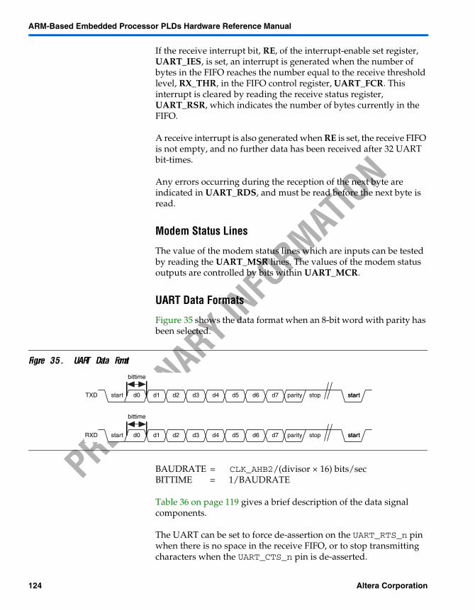
ARM-Based Embedded Processor PLDs Hardware Reference Manual
PRELIM
INARY IN
FORMAT
ION
If the receive interrupt bit, RE, of the interrupt-enable set register, UART_IES, is set, an interrupt is generated when the number of bytes in the FIFO reaches the number equal to the receive threshold level, RX_THR, in the FIFO control register, UART_FCR. This interrupt is cleared by reading the receive status register, UART_RSR, which indicates the number of bytes currently in the FIFO.
A receive interrupt is also generated when RE is set, the receive FIFO is not empty, and no further data has been received after 32 UART bit-times.
Any errors occurring during the reception of the next byte are indicated in UART_RDS, and must be read before the next byte is read.
Modem Status Lines
The value of the modem status lines which are inputs can be tested by reading the UART_MSR lines. The values of the modem status outputs are controlled by bits within UART_MCR.
UART Data Formats
Figure 35 shows the data format when an 8-bit word with parity has been selected.
Figure 35. UART Data Format
BAUDRATE = CLK_AHB2/(divisor × 16) bits/secBITTIME = 1/BAUDRATE
Table 36 on page 119 gives a brief description of the data signal components.
The UART can be set to force de-assertion on the UART_RTS_n pin when there is no space in the receive FIFO, or to stop transmitting characters when the UART_CTS_n pin is de-asserted.
TXD
RXD
start d0 d1 d2 d3 d4 d5 d6 d7 parity stop startstart
start d0 d1 d2 d3 d4 d5 d6 d7 parity stop startstart
bittime
bittime
124 Altera Corporation
ARM-Based Embedded Processor PLDs Hardware Reference Manual
PRELIM
INARY IN
FORMAT
ION
Registers
At reset, all registers hold the value 0 unless otherwise specified.
Register: UART_RSR (receive status register)Address: Register base + 280HAccess: Read
Reading this register resets the receive-interrupt bit, RI, in UART_ISR.
Table 36. Data Signal Components
START_BIT UART_TXD and UART_RXD are normally high. When a character is being transmitted, UART_TXD is driven low for the duration of 1-bit time. The receiver always samples the UART_RXD line. When it detects a start bit, it starts shifting a new character in
DATA A character can be programmed for 5 to 8 bits. Both transmitting and receiving UARTs must be programmed for the same settings, otherwise communication fails
PARITY Parity generation and checking can be enabled or disabled. If parity is disabled, no parity bit is transmitted, and the receiver does not expect to receive a parity bit. If parity is enabled, it can be even, odd, or stick parity:Even parity—Parity bit is 1, if the character has an odd number of 1sOdd parity—Parity bit is 1, if the character has an even number of 1sStick parity—Parity bit can be forced to 1 or 0
STOP BIT Stop bits are the last bits to be transmitted or received for each character. A stop bit is a 1. The number of stop bits can be programmed to be 1- or 2-bit times. Stop bits act like a spacer between characters if they are transmitted back-to-back. Both receiving and transmitting UARTs must be programmed for the same settings. The UART only checks the first stop bit
BREAK A break is detected if UART_RXD is held low longer than a character-time. (A character-time is the time to transmit or receive a character including start, parity and stop bits.) This usually happens if UART_RXD is disconnected, or the transmitting UART forced a break or is turned off. A break can be forced by setting the break bit in the modem control register, UART_MCR
RX_LEVEL R* The number of bytes in the receive FIFO
0 R Reserved for future use
12345678910111213141516171819202122232425262728293031 0
0 RX_LEVEL
Altera Corporation 125
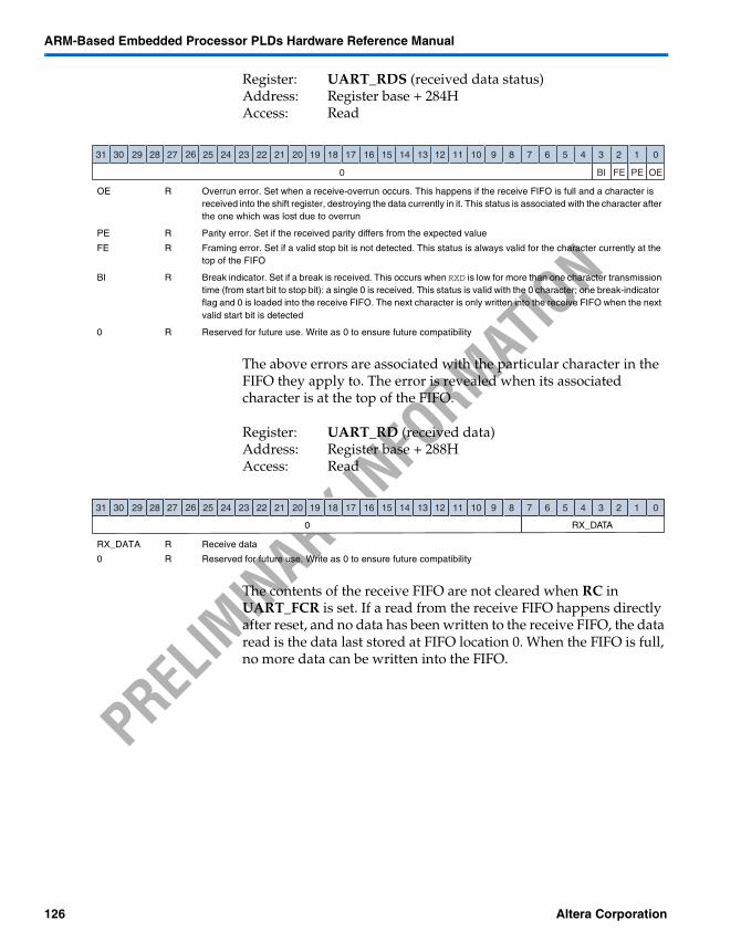
ARM-Based Embedded Processor PLDs Hardware Reference Manual
PRELIM
INARY IN
FORMAT
ION
Register: UART_RDS (received data status)Address: Register base + 284HAccess: Read
The above errors are associated with the particular character in the FIFO they apply to. The error is revealed when its associated character is at the top of the FIFO.
Register: UART_RD (received data)Address: Register base + 288HAccess: Read
The contents of the receive FIFO are not cleared when RC in UART_FCR is set. If a read from the receive FIFO happens directly after reset, and no data has been written to the receive FIFO, the data read is the data last stored at FIFO location 0. When the FIFO is full, no more data can be written into the FIFO.
OE R Overrun error. Set when a receive-overrun occurs. This happens if the receive FIFO is full and a character is received into the shift register, destroying the data currently in it. This status is associated with the character after the one which was lost due to overrun
PE R Parity error. Set if the received parity differs from the expected value
FE R Framing error. Set if a valid stop bit is not detected. This status is always valid for the character currently at the top of the FIFO
BI R Break indicator. Set if a break is received. This occurs when RXD is low for more than one character transmission time (from start bit to stop bit): a single 0 is received. This status is valid with the 0 character; one break-indicator flag and 0 is loaded into the receive FIFO. The next character is only written into the receive FIFO when the next valid start bit is detected
0 R Reserved for future use. Write as 0 to ensure future compatibility
12345678910111213141516171819202122232425262728293031 0
0 BI FE PE OE
RX_DATA R Receive data
0 R Reserved for future use. Write as 0 to ensure future compatibility
12345678910111213141516171819202122232425262728293031 0
0 RX_DATA
126 Altera Corporation
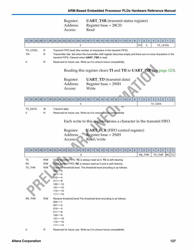
ARM-Based Embedded Processor PLDs Hardware Reference Manual
PRELIM
INARY IN
FORMAT
ION
Register: UART_TSR (transmit status register)Address: Register base + 28CH Access: Read
Reading this register clears TI and TII in UART_ISR (see page 123).
Register: UART_TD (transmit data)Address: Register base + 290HAccess: Write
Each write to this register stores a character in the transmit FIFO.
Register: UART_FCR (FIFO control register)Address: Register base + 294HAccess: Read/write
TX_LEVEL R Transmit FIFO level (the number of characters in the transmit FIFO)
TXI R Transmitter idle. Set when the transmitter shift register becomes empty and there are no more characters in the transmit FIFO. Cleared when UART_TSR is read
0 R Reserved for future use. Write as 0 to ensure future compatibility
12345678910111213141516171819202122232425262728293031 0
0 TXI 0 TX_LEVEL
TX_DATA W Transmit data
0 R Reserved for future use. Write as 0 to ensure future compatibility
12345678910111213141516171819202122232425262728293031 0
0 TX_DATA
TC R/W Clear transmit FIFO. TC is always read as 0. TC is self-clearing
RC R/W Clear receive FIFO. RC is always read as 0 and is self-clearing
TX_THR R/W Transmit threshold level. The threshold level encoding is as follows:000—0001—2010—4011—8100—10101—12110—14111—15
RX_THR R/W Receive threshold level.The threshold level encoding is as follows:000—1001—2010—4011—6100—8101—10110—12111—14
0 R Reserved for future use. Write as 0 to ensure future compatibility
12345678910111213141516171819202122232425262728293031 0
0 RX_THR TX_THR RC TC
Altera Corporation 127
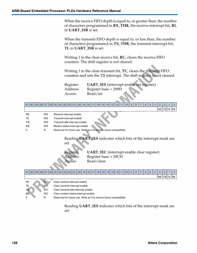
ARM-Based Embedded Processor PLDs Hardware Reference Manual
PRELIM
INARY IN
FORMAT
ION
When the receive FIFO depth is equal to, or greater than, the number of characters programmed in RX_THR, the receive-interrupt bit, RI, in UART_ISR is set.
When the transmit FIFO depth is equal to, or less than, the number of characters programmed in TX_THR, the transmit-interrupt bit, TI, in UART_ISR is set.
Writing 1 to the clear-receive bit, RC, clears the receive FIFO counters. The shift register is not cleared.
Writing 1 to the clear-transmit bit, TC, clears the transmit FIFO counters and sets the TII interrupt. The shift register is not cleared.
Register: UART_IES (interrupt-enable set register)Address: Register base + 298HAccess: Read/set
Reading UART_IES indicates which bits of the interrupt mask are set.
Register: UART_IEC (interrupt-enable clear register)Address: Register base + 29CHAccess: Read/clear
Reading UART_IES indicates which bits of the interrupt mask are set.
RE R/S Receive-interrupt enable
TE R/S Transmit-interrupt enable
TIE R/S Transmit-idle-interrupt enable
ME R/S Modem-status-interrupt enable
0 R Reserved for future use. Write as 0 to ensure future compatibility
12345678910111213141516171819202122232425262728293031 0
RETETIEME
RE R/C Clear receive-interrupt enable
TE R/C Clear transmit-interrupt enable
TIE R/C Clear transmit-idle-interrupt enable
ME R/C Clear modem-status-interrupt enable
0 R Reserved for future use. Write as 0 to ensure future compatibility
12345678910111213141516171819202122232425262728293031 0
RETETIEME
128 Altera Corporation
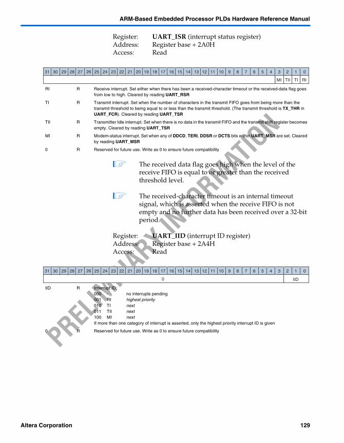
ARM-Based Embedded Processor PLDs Hardware Reference Manual
PRELIM
INARY IN
FORMAT
ION
Register: UART_ISR (interrupt status register)Address: Register base + 2A0HAccess: Read
The received data flag goes high when the level of the receive FIFO is equal to or greater than the received threshold level.
The received-character timeout is an internal timeout signal, which is asserted when the receive FIFO is not empty and no further data has been received over a 32-bit period.
Register: UART_IID (interrupt ID register)Address: Register base + 2A4HAccess: Read
RI R Receive interrupt. Set either when there has been a received-character timeout or the received-data flag goes from low to high. Cleared by reading UART_RSR
TI R Transmit interrupt. Set when the number of characters in the transmit FIFO goes from being more than the transmit threshold to being equal to or less than the transmit threshold. (The transmit threshold is TX_THR in UART_FCR). Cleared by reading UART_TSR
TII R Transmitter Idle interrupt. Set when there is no data in the transmit FIFO and the transmit shift register becomes empty. Cleared by reading UART_TSR
MI R Modem-status interrupt. Set when any of DDCD, TERI, DDSR or DCTS bits within UART_MSR are set. Cleared by reading UART_MSR
0 R Reserved for future use. Write as 0 to ensure future compatibility
12345678910111213141516171819202122232425262728293031 0
RITITIIMI
IID R Interrupt ID:000 - no interrupts pending001 RI highest priority010 TI next011 TII next100 MI nextIf more than one category of interrupt is asserted, only the highest priority interrupt ID is given
0 R Reserved for future use. Write as 0 to ensure future compatibility
12345678910111213141516171819202122232425262728293031 0
0 IID
Altera Corporation 129
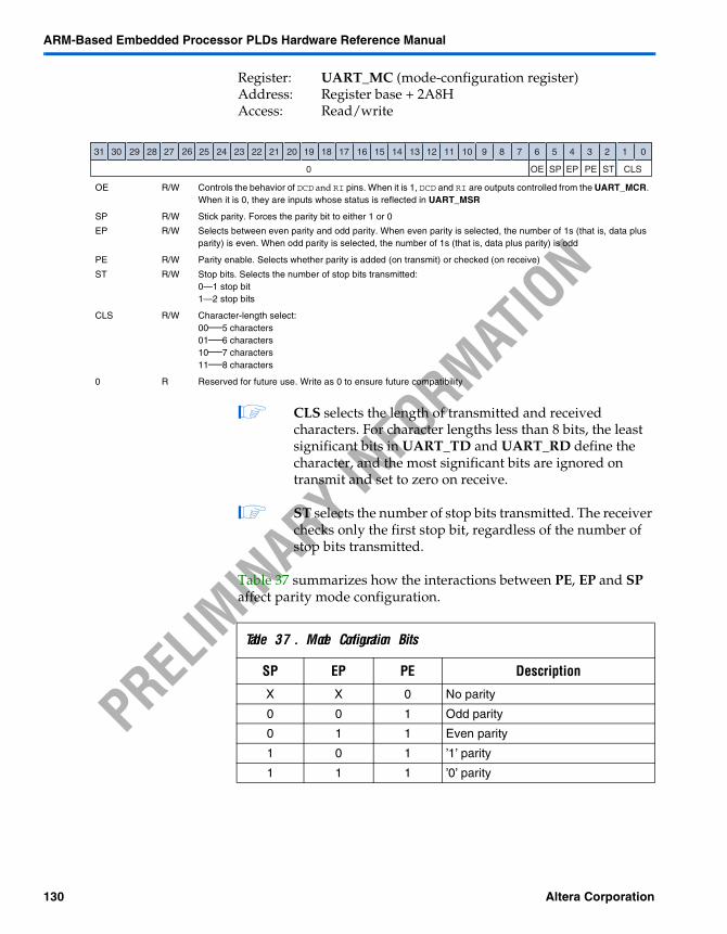
ARM-Based Embedded Processor PLDs Hardware Reference Manual
PRELIM
INARY IN
FORMAT
ION
Register: UART_MC (mode-configuration register)Address: Register base + 2A8HAccess: Read/write
CLS selects the length of transmitted and received characters. For character lengths less than 8 bits, the least significant bits in UART_TD and UART_RD define the character, and the most significant bits are ignored on transmit and set to zero on receive.
ST selects the number of stop bits transmitted. The receiver checks only the first stop bit, regardless of the number of stop bits transmitted.
Table 37 summarizes how the interactions between PE, EP and SP affect parity mode configuration.
OE R/W Controls the behavior of DCD and RI pins. When it is 1, DCD and RI are outputs controlled from the UART_MCR. When it is 0, they are inputs whose status is reflected in UART_MSR
SP R/W Stick parity. Forces the parity bit to either 1 or 0
EP R/W Selects between even parity and odd parity. When even parity is selected, the number of 1s (that is, data plus parity) is even. When odd parity is selected, the number of 1s (that is, data plus parity) is odd
PE R/W Parity enable. Selects whether parity is added (on transmit) or checked (on receive)
ST R/W Stop bits. Selects the number of stop bits transmitted:0—1 stop bit1—2 stop bits
CLS R/W Character-length select:00—5 characters01—6 characters10—7 characters11—8 characters
0 R Reserved for future use. Write as 0 to ensure future compatibility
12345678910111213141516171819202122232425262728293031 0
OE SP EP PE ST CLS0
Table 37. Mode Configuration Bits
SP EP PE Description
X X 0 No parity
0 0 1 Odd parity
0 1 1 Even parity
1 0 1 ’1’ parity
1 1 1 ’0’ parity
130 Altera Corporation
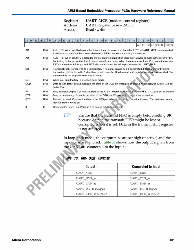
ARM-Based Embedded Processor PLDs Hardware Reference Manual
PRELIM
INARY IN
FORMAT
ION
Register: UART_MCR (modem control register)Address: UART Register base + 2ACHAccess: Read/write
Ensure that the transmit FIFO is empty before setting BR, because data in the transmit FIFO might be lost or corrupted when it is set. Data in the transmit shift register is not affected.
In loop-back mode, the output pins are set high (inactive) and the input pins are ignored. Table 38 shows how the output signals from the UART are connected to the inputs.
AC R/W Auto CTS. When set, the transmitter does not start to transmit a character if CTS in UART_MSR is not asserted. It continues to transmit the current character if CTS changes state during a character.
AR R/W Auto RTS. When set, RTS is forced to the de-asserted state when there are 15 bytes or more in the receive FIFO (indicating to the transmitter that it cannot accept new data). When there are fewer than 15 bytes in the receive FIFO, the state of AR is ignored. RTS also depends on the value programmed in UART_MCR
BR R/W Transmit break. Forces TXD to 0 immediately if no serial data is being transmitted. If data is currently being transmitted, TXD is forced to 0 after the current contents of the transmit shift register have been transmitted. The transmitter is not stopped when this bit is set
LB R/W When set, puts the UART into loop-back mode
DCD R/W Data carrier detect output. Controls the state of the DCD pin when it is an output. When DCD is 1, DCD_n is set active-low
RI R/W Ring indicator output. Controls the state of the RI pin, when it is an output. When RI is 1, RI_n is set active-low
DTR R/W Data terminal ready. Controls the state of the DTR pin. When it is 1, DTR_n is set active-low
RTS R/W Request to send. Controls the state of the RTS pin. When it is 1, RTS_n is set active-low. Can be forced into an inactive state if AR is set
0 R Reserved for future use. Write as 0 to ensure future compatibility
12345678910111213141516171819202122232425262728293031 0
RTSDTRRIDCDLBBRARAC0
Table 38. Input-Output Connections
Output Connected to Input
UART_TXD UART_RXD
UART_RTS_n UART_CTS_n
UART_DTR_n UART_DSR_n
UART_RI_n output UART_RI_n input
UART_DCD_n output UART_DCD_n input
Altera Corporation 131
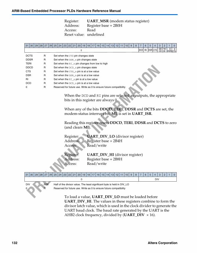
ARM-Based Embedded Processor PLDs Hardware Reference Manual
PRELIM
INARY IN
FORMAT
ION
Register: UART_MSR (modem status register)Address: Register base + 2B0HAccess: ReadReset value: undefined
When the DCD and RI pins are selected as outputs, the appropriate bits in this register are always 0.
When any of the bits DDCD, TERI, DDSR and DCTS are set, the modem-status interrupt bit, MI, is set in UART_ISR.
Reading this register resets DDCD, TERI, DDSR and DCTS to zero (and clears MI).
Register: UART_DIV_LO (divisor register)Address: Register base + 2B4HAccess: Read/write
Register: UART_DIV_HI (divisor register)Address: Register base + 2B8HAccess: Read/write
To load a value, UART_DIV_LO must be loaded before UART_DIV_HI. The values in these registers combine to form the divisor latch value, which is used in the clock divider to generate the UART baud clock. The baud rate generated by the UART is the AHB2 clock frequency, divided by (UART_DIV × 16).
DCTS R Set when the CTS pin changes state
DDSR R Set when the DSR_n pin changes state
TERI R Set when the RI_n pin changes from low to high
DDCD R Set when the DCD_n pin changes state
CTS R Set when the CTS_n pin is at a low value
DSR R Set when the DSR_n pin is at a low value
RI R Set when the RI_n pin is at a low value
DCD R Set when the DCD_n pin is at a low value
0 R Reserved for future use. Write as 0 to ensure future compatibility
12345678910111213141516171819202122232425262728293031 0D
CTSD
DSRTERI
DDCDCTSDSRRIDCD0
DIV R/W Half of the divisor value. The least significant byte is held in DIV_LO
0 R Reserved for future use. Write as 0 to ensure future compatibility
12345678910111213141516171819202122232425262728293031 0
0 DIV
132 Altera Corporation
ARM-Based Embedded Processor PLDs Hardware Reference Manual
PRELIM
INARY IN
FORMAT
ION
If a divisor value of 0 or 1 is programmed, the baud rate divisor divides by 2. For example, to generate a baud rate of 230,400 from an AHB2 clock of 33 Mhz. the ideal divisor is:
33,000,000/(16 × 230,400) = 8.95
A programmed value of 9 gives a 0.5% error from the ideal baud rate, which is comfortably within the bounds allowed by the RS232 specification.
Debug Support Various features are provided to aid in debugging soft logic and running code, including the following:
SignalTap logic analyzer module JTAG access to AHB2 bus JTAG communications link between host and embedded
processor Debug signals available in the PLD
JTAG support
The PLD TAP controller allows boundary scans of the physical pins and configuration-bit downloading into the PLD bits. The embedded processor provides a second TAP controller, which gives a debugger access to the internal state of the embedded processor and provides extensive debugging functionality.
There are two JTAG configurations:
Dual-JTAG mode Single-JTAG mode
In dual-JTAG mode, the PLD TAP controller is connected to the TMS, TDO, TDI, TCK, and nTRST pins, and the processor TAP controller is connected to the PROC_TMS, PROC_TDO, PROC_TDI, PROC_TCK, and PROC_nTRST pins.
In single-JTAG modes, the PLD TAP controller is followed by the embedded processor TAP controller.
Figures 36 and 37 on page 128 show the JTAG configurations.
Altera Corporation 133
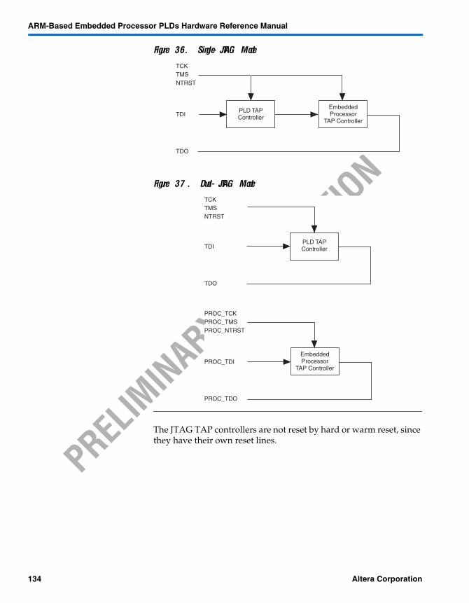
ARM-Based Embedded Processor PLDs Hardware Reference Manual
PRELIM
INARY IN
FORMAT
ION
Figure 36. Single-JTAG Mode
Figure 37. Dual-JTAG Mode
The JTAG TAP controllers are not reset by hard or warm reset, since they have their own reset lines.
PLD TAPController
EmbeddedProcessor
TAP Controller
TCKTMSNTRST
TDI
TDO
PLD TAPController
EmbeddedProcessor
TAP Controller
TCKTMSNTRST
TDI
TDO
PROC_TCKPROC_TMSPROC_NTRST
PROC_TDI
PROC_TDO
134 Altera Corporation
ARM-Based Embedded Processor PLDs Hardware Reference Manual
PRELIM
INARY IN
FORMAT
ION
SignalTap Embedded Logic Analyzer
The programmable core includes enhancements to support the SignalTap™ embedded logic analyzer. By including this circuitry, the ARM-based device provides the ability to monitor design operation over a period of time through the IEEE Std. 1149.1 (JTAG) circuitry; a designer can analyze internal logic at speed without bringing internal signals to the I/O pins. This feature is particularly important for advanced packages such as FineLine BGA packages, because it can be difficult to add a connection to a pin during the debugging process after a board is designed and manufactured.
IEEE Std. 1149.1 (JTAG) Boundary-Scan Support
The ARM-based devices provide JTAG BST circuitry that complies with the IEEE Std. 1149.1-1990 specification. JTAG boundary-scan testing can be performed before or after configuration, but not during configuration. The ARM-based devices can also use the JTAG port for configuration with the Quartus software or with hardware using either Jam Files (.jam) or Jam Byte-Code Files (.jbc). Finally, the ARM-based devices use the JTAG port to monitor the logic operation of the device with the SignalTap embedded logic analyzer. The ARM-based devices support the JTAG instructions shown in Table 39 on page 130.
Altera Corporation 135
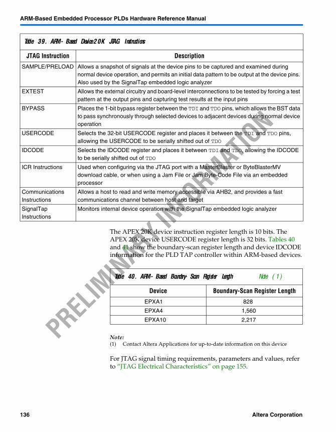
ARM-Based Embedded Processor PLDs Hardware Reference Manual
PRELIM
INARY IN
FORMAT
ION
The APEX 20K device instruction register length is 10 bits. The APEX 20K device USERCODE register length is 32 bits. Tables 40 and 41 show the boundary-scan register length and device IDCODE information for the PLD TAP controller within ARM-based devices.
Note:(1) Contact Altera Applications for up-to-date information on this device
For JTAG signal timing requirements, parameters and values, refer to “JTAG Electrical Characteristics” on page 155.
Table 39. ARM-Based Device 20K JTAG Instructions
JTAG Instruction Description
SAMPLE/PRELOAD Allows a snapshot of signals at the device pins to be captured and examined during normal device operation, and permits an initial data pattern to be output at the device pins. Also used by the SignalTap embedded logic analyzer
EXTEST Allows the external circuitry and board-level interconnections to be tested by forcing a test pattern at the output pins and capturing test results at the input pins
BYPASS Places the 1-bit bypass register between the TDI and TDO pins, which allows the BST data to pass synchronously through selected devices to adjacent devices during normal device operation
USERCODE Selects the 32-bit USERCODE register and places it between the TDI and TDO pins, allowing the USERCODE to be serially shifted out of TDO
IDCODE Selects the IDCODE register and places it between TDI and TDO, allowing the IDCODE to be serially shifted out of TDO
ICR Instructions Used when configuring via the JTAG port with a MasterBlaster or ByteBlasterMV download cable, or when using a Jam File or Jam Byte-Code File via an embedded processor
Communications Instructions
Allows a host to read and write memory accessible via AHB2, and provides a fast communications channel between host and target
SignalTap Instructions
Monitors internal device operation with the SignalTap embedded logic analyzer
Table 40. ARM-Based Boundary-Scan Register Length Note (1)
Device Boundary-Scan Register Length
EPXA1 828
EPXA4 1,560
EPXA10 2,217
136 Altera Corporation
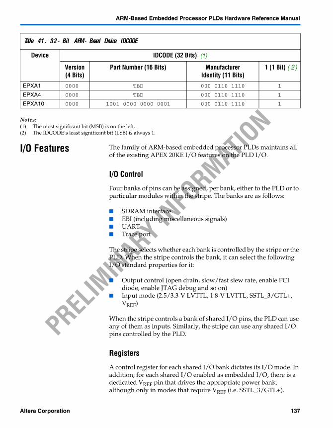
ARM-Based Embedded Processor PLDs Hardware Reference Manual
PRELIM
INARY IN
FORMAT
IONNotes:
(1) The most significant bit (MSB) is on the left.(2) The IDCODE’s least significant bit (LSB) is always 1.
I/O Features The family of ARM-based embedded processor PLDs maintains all of the existing APEX 20KE I/O features on the PLD I/O.
I/O Control
Four banks of pins can be assigned, per bank, either to the PLD or to particular modules within the stripe. The banks are as follows:
SDRAM interface EBI (including miscellaneous signals) UART Trace port
The stripe selects whether each bank is controlled by the stripe or the PLD. When the stripe controls the bank, it can select the following I/O standard properties for it:
Output control (open drain, slow/fast slew rate, enable PCI diode, enable JTAG debug and so on)
Input mode (2.5/3.3-V LVTTL, 1.8-V LVTTL, SSTL_3/GTL+, VREF)
When the stripe controls a bank of shared I/O pins, the PLD can use any of them as inputs. Similarly, the stripe can use any shared I/O pins controlled by the PLD.
Registers
A control register for each shared I/O bank dictates its I/O mode. In addition, for each shared I/O enabled as embedded I/O, there is a dedicated VREF pin that drives the appropriate power bank, although only in modes that require VREF (i.e. SSTL_3/GTL+).
Table 41. 32-Bit ARM-Based Device IDCODE
Device IDCODE (32 Bits) (1)
Version (4 Bits)
Part Number (16 Bits) ManufacturerIdentity (11 Bits)
1 (1 Bit) (2)
EPXA1 0000 TBD 000 0110 1110 1
EPXA4 0000 TBD 000 0110 1110 1
EPXA10 0000 1001 0000 0000 0001 000 0110 1110 1
Altera Corporation 137
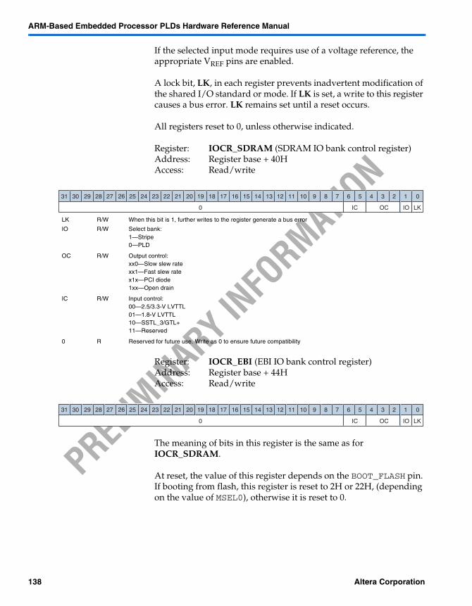
ARM-Based Embedded Processor PLDs Hardware Reference Manual
PRELIM
INARY IN
FORMAT
ION
If the selected input mode requires use of a voltage reference, the appropriate VREF pins are enabled.
A lock bit, LK, in each register prevents inadvertent modification of the shared I/O standard or mode. If LK is set, a write to this register causes a bus error. LK remains set until a reset occurs.
All registers reset to 0, unless otherwise indicated.
Register: IOCR_SDRAM (SDRAM IO bank control register)Address: Register base + 40HAccess: Read/write
Register: IOCR_EBI (EBI IO bank control register)Address: Register base + 44HAccess: Read/write
The meaning of bits in this register is the same as for IOCR_SDRAM.
At reset, the value of this register depends on the BOOT_FLASH pin. If booting from flash, this register is reset to 2H or 22H, (depending on the value of MSEL0), otherwise it is reset to 0.
LK R/W When this bit is 1, further writes to the register generate a bus error
IO R/W Select bank:1—Stripe0—PLD
OC R/W Output control:xx0—Slow slew ratexx1—Fast slew ratex1x—PCI diode1xx—Open drain
IC R/W Input control:00—2.5/3.3-V LVTTL01—1.8-V LVTTL10—SSTL_3/GTL+11—Reserved
0 R Reserved for future use. Write as 0 to ensure future compatibility
12345678910111213141516171819202122232425262728293031 0
0 IC OC IO LK
12345678910111213141516171819202122232425262728293031 0
0 IC OC IO LK
138 Altera Corporation
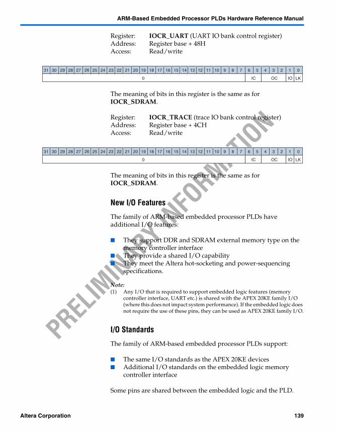
ARM-Based Embedded Processor PLDs Hardware Reference Manual
PRELIM
INARY IN
FORMAT
ION
Register: IOCR_UART (UART IO bank control register)Address: Register base + 48HAccess: Read/write
The meaning of bits in this register is the same as for IOCR_SDRAM.
Register: IOCR_TRACE (trace IO bank control register)Address: Register base + 4CHAccess: Read/write
The meaning of bits in this register is the same as for IOCR_SDRAM.
New I/O Features
The family of ARM-based embedded processor PLDs have additional I/O features:
They support DDR and SDRAM external memory type on the memory controller interface
They provide a shared I/O capability They meet the Altera hot-socketing and power-sequencing
specifications.
Note:(1) Any I/O that is required to support embedded logic features (memory
controller interface, UART etc.) is shared with the APEX 20KE family I/O (where this does not impact system performance). If the embedded logic does not require the use of these pins, they can be used as APEX 20KE family I/O.
I/O Standards
The family of ARM-based embedded processor PLDs support:
The same I/O standards as the APEX 20KE devices Additional I/O standards on the embedded logic memory
controller interface
Some pins are shared between the embedded logic and the PLD.
12345678910111213141516171819202122232425262728293031 0
0 IC OC IO LK
12345678910111213141516171819202122232425262728293031 0
0 IC OC IO LK
Altera Corporation 139
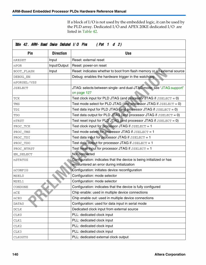
ARM-Based Embedded Processor PLDs Hardware Reference Manual
PRELIM
INARY IN
FORMAT
ION
If a block of I/O is not used by the embedded logic, it can be used by the PLD array. Dedicated I/O and APEX 20KE dedicated I/O are listed in Table 42.
Table 42. ARM-Based Device Dedicated I/O Pins (Part 1 of 2)
Pin Direction Use
nRESET Input Reset: external reset
nPOR Input/Output Reset: power-on reset
BOOT_FLASH Input Reset: indicates whether to boot from flash memory or an external source
DEBUG_EN Debug: enables the hardware trigger in the watchdog
nPORSEL/VSS
JSELECT JTAG: selects between single- and dual-JTAG mode; see “JTAG support” on page 127
TCK Test clock input for PLD JTAG (and processor JTAG if JSELECT = 0)
TMS Test mode select for PLD JTAG (and processor JTAG if JSELECT = 0)
TDI Test data input for PLD JTAG (and processor JTAG if JSELECT = 0)
TDO Test data output for PLD JTAG (and processor JTAG if JSELECT = 0)
nTRST Test reset input for PLD JTAG (and processor JTAG if JSELECT = 0)
PROC_TCK Test clock input for processor JTAG if JSELECT = 1
PROC_TMS Test mode select for processor JTAG if JSELECT = 1
PROC_TDI Test data input for processor JTAG if JSELECT = 1
PROC_TDO Test data output for processor JTAG if JSELECT = 1
PROC_NTRST Test reset input for processor JTAG if JSELECT = 1
EN_SELECT Not connected
nSTATUS Configuration: indicates that the device is being initialized or has encountered an error during initialization
nCONFIG Configuration: initiates device reconfiguration
MSEL0 Configuration: mode selector
MSEL1 Configuration: mode selector
CONDONE Configuration: indicates that the device is fully configured
nCE Chip enable: used in multiple device connections
nCEO Chip enable out: used in multiple device connections
DATA0 Configuration: used for data input in serial mode
DCLK Dedicated clock input from external source
CLK0 PLL: dedicated clock input
CLK1 PLL: dedicated clock input
CLK2 PLL: dedicated clock input
CLK3 PLL: dedicated clock input
CLKOUT0 PLL: dedicated external clock output
140 Altera Corporation
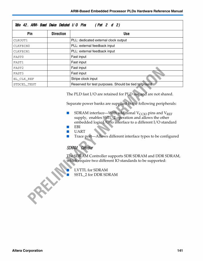
ARM-Based Embedded Processor PLDs Hardware Reference Manual
PRELIM
INARY IN
FORMAT
ION
The PLD fast I/O are retained for PLD use and are not shared.
Separate power banks are supplied to the following peripherals:
SDRAM interface—With additional VCCIO pins and VREF supply, enables SSTL_2 operation and allows the other embedded logic I/O to interface to a different I/O standard
EBI UART Trace port—Allows different interface types to be configured
SDRAM Controller
The SDRAM Controller supports SDR SDRAM and DDR SDRAM, which require two different IO standards to be supported:
LVTTL for SDRAM SSTL_2 for DDR SDRAM
CLKOUT1 PLL: dedicated external clock output
CLKFBIN0 PLL: external feedback input
CLKFBIN1 PLL: external feedback input
FAST0 Fast input
FAST1 Fast input
FAST2 Fast input
FAST3 Fast input
EL_CLK_REF Stripe clock input
STDCEL_TEST Reserved for test purposes. Should be tied to ground
Table 42. ARM-Based Device Dedicated I/O Pins (Part 2 of 2)
Pin Direction Use
Altera Corporation 141
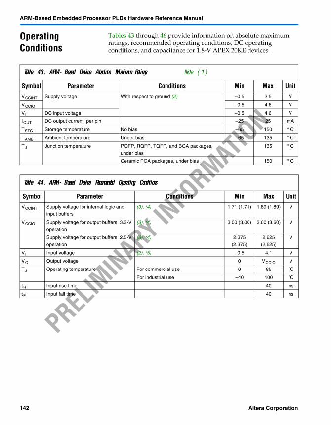
ARM-Based Embedded Processor PLDs Hardware Reference Manual
PRELIM
INARY IN
FORMAT
ION
Operating Conditions
Tables 43 through 46 provide information on absolute maximum ratings, recommended operating conditions, DC operating conditions, and capacitance for 1.8-V APEX 20KE devices.
Table 43. ARM-Based Device Absolute Maximum Ratings Note (1)
Symbol Parameter Conditions Min Max Unit
VCCINT Supply voltage With respect to ground (2) –0.5 2.5 V
VCCIO –0.5 4.6 V
VI DC input voltage –0.5 4.6 V
IOUT DC output current, per pin –25 25 mA
TSTG Storage temperature No bias –65 150 ° C
TAMB Ambient temperature Under bias –65 135 ° C
TJ Junction temperature PQFP, RQFP, TQFP, and BGA packages, under bias
135 ° C
Ceramic PGA packages, under bias 150 ° C
Table 44. ARM-Based Device Recommended Operating Conditions
Symbol Parameter Conditions Min Max UnitVCCINT Supply voltage for internal logic and
input buffers(3), (4) 1.71 (1.71) 1.89 (1.89) V
VCCIO Supply voltage for output buffers, 3.3-V operation
(3), (4) 3.00 (3.00) 3.60 (3.60) V
Supply voltage for output buffers, 2.5-V operation
(3), (4) 2.375 (2.375)
2.625 (2.625)
V
VI Input voltage (2), (5) –0.5 4.1 V
VO Output voltage 0 VCCIO V
TJ Operating temperature For commercial use 0 85 °C
For industrial use –40 100 °C
tR Input rise time 40 ns
tF Input fall time 40 ns
142 Altera Corporation
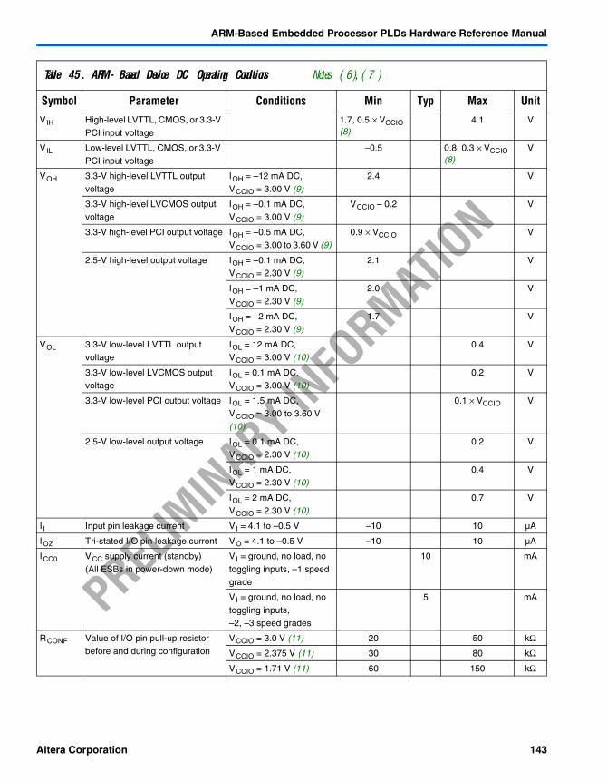
ARM-Based Embedded Processor PLDs Hardware Reference Manual
PRELIM
INARY IN
FORMAT
ION
Table 45. ARM-Based Device DC Operating Conditions Notes (6), (7)
Symbol Parameter Conditions Min Typ Max UnitVIH High-level LVTTL, CMOS, or 3.3-V
PCI input voltage
1.7, 0.5 × VCCIO (8)
4.1 V
VIL Low-level LVTTL, CMOS, or 3.3-V
PCI input voltage
–0.5 0.8, 0.3 × VCCIO (8)
V
VOH 3.3-V high-level LVTTL output
voltage
IOH = –12 mA DC,
VCCIO = 3.00 V (9)
2.4 V
3.3-V high-level LVCMOS output voltage
IOH = –0.1 mA DC, VCCIO = 3.00 V (9)
VCCIO – 0.2 V
3.3-V high-level PCI output voltage IOH = –0.5 mA DC, VCCIO = 3.00 to 3.60 V (9)
0.9 × VCCIO V
2.5-V high-level output voltage IOH = –0.1 mA DC, VCCIO = 2.30 V (9)
2.1 V
IOH = –1 mA DC, VCCIO = 2.30 V (9)
2.0 V
IOH = –2 mA DC, VCCIO = 2.30 V (9)
1.7 V
VOL 3.3-V low-level LVTTL output voltage
IOL = 12 mA DC, VCCIO = 3.00 V (10)
0.4 V
3.3-V low-level LVCMOS output voltage
IOL = 0.1 mA DC, VCCIO = 3.00 V (10)
0.2 V
3.3-V low-level PCI output voltage IOL = 1.5 mA DC, VCCIO = 3.00 to 3.60 V (10)
0.1 × VCCIO V
2.5-V low-level output voltage IOL = 0.1 mA DC, VCCIO = 2.30 V (10)
0.2 V
IOL = 1 mA DC, VCCIO = 2.30 V (10)
0.4 V
IOL = 2 mA DC, VCCIO = 2.30 V (10)
0.7 V
II Input pin leakage current VI = 4.1 to –0.5 V –10 10 µA
IOZ Tri-stated I/O pin leakage current VO = 4.1 to –0.5 V –10 10 µA
ICC0 VCC supply current (standby)
(All ESBs in power-down mode)
VI = ground, no load, no
toggling inputs, –1 speed grade
10 mA
VI = ground, no load, no
toggling inputs,–2, –3 speed grades
5 mA
RCONF Value of I/O pin pull-up resistor before and during configuration
VCCIO = 3.0 V (11) 20 50 kΩ
VCCIO = 2.375 V (11) 30 80 kΩ
VCCIO = 1.71 V (11) 60 150 kΩ
Altera Corporation 143
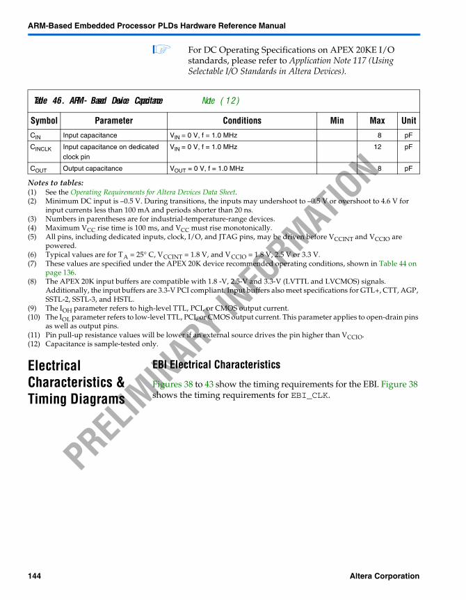
ARM-Based Embedded Processor PLDs Hardware Reference Manual
PRELIM
INARY IN
FORMAT
ION
For DC Operating Specifications on APEX 20KE I/O standards, please refer to Application Note 117 (Using Selectable I/O Standards in Altera Devices).
Notes to tables:(1) See the Operating Requirements for Altera Devices Data Sheet.(2) Minimum DC input is –0.5 V. During transitions, the inputs may undershoot to –0.5 V or overshoot to 4.6 V for
input currents less than 100 mA and periods shorter than 20 ns.(3) Numbers in parentheses are for industrial-temperature-range devices.(4) Maximum VCC rise time is 100 ms, and VCC must rise monotonically.(5) All pins, including dedicated inputs, clock, I/O, and JTAG pins, may be driven before VCCINT and VCCIO are
powered.(6) Typical values are for TA = 25° C, VCCINT = 1.8 V, and VCCIO = 1.8 V, 2.5 V or 3.3 V.(7) These values are specified under the APEX 20K device recommended operating conditions, shown in Table 44 on
page 136.(8) The APEX 20K input buffers are compatible with 1.8 -V, 2.5-V and 3.3-V (LVTTL and LVCMOS) signals.
Additionally, the input buffers are 3.3-V PCI compliant. Input buffers also meet specifications for GTL+, CTT, AGP, SSTL-2, SSTL-3, and HSTL.
(9) The IOH parameter refers to high-level TTL, PCI, or CMOS output current.(10) The IOL parameter refers to low-level TTL, PCI, or CMOS output current. This parameter applies to open-drain pins
as well as output pins.(11) Pin pull-up resistance values will be lower if an external source drives the pin higher than VCCIO.(12) Capacitance is sample-tested only.
Electrical Characteristics & Timing Diagrams
EBI Electrical Characteristics
Figures 38 to 43 show the timing requirements for the EBI. Figure 38 shows the timing requirements for EBI_CLK.
Table 46. ARM-Based Device Capacitance Note (12)
Symbol Parameter Conditions Min Max Unit
CIN Input capacitance VIN = 0 V, f = 1.0 MHz 8 pF
CINCLK Input capacitance on dedicated
clock pin
VIN = 0 V, f = 1.0 MHz 12 pF
COUT Output capacitance VOUT = 0 V, f = 1.0 MHz 8 pF
144 Altera Corporation
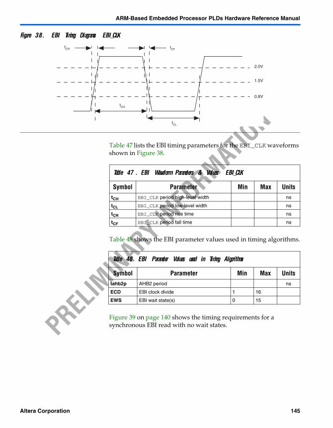
ARM-Based Embedded Processor PLDs Hardware Reference Manual
PRELIM
INARY IN
FORMAT
ION
Figure 38. EBI Timing Diagrams: EBI_CLK
Table 47 lists the EBI timing parameters for the EBI_CLK waveforms shown in Figure 38.
Table 48 shows the EBI parameter values used in timing algorithms.
Figure 39 on page 140 shows the timing requirements for a synchronous EBI read with no wait states.
2.0V
1.5V
0.8V
tCR tCF
tCH
tCL
Table 47. EBI Waveform Parameters & Values: EBI_CLK
Symbol Parameter Min Max UnitstCH EBI_CLK period high-level width ns
tCL EBI_CLK period low-level width ns
tCR EBI_CLK period rise time ns
tCF EBI_CLK period fall time ns
Table 48. EBI Parameter Values used in Timing Algorithms
Symbol Parameter Min Max Unitstahb2p AHB2 period ns
ECD EBI clock divide 1 16
EWS EBI wait state(s) 0 15
Altera Corporation 145
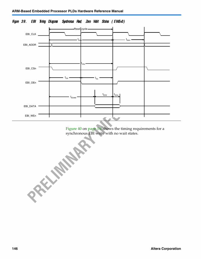
ARM-Based Embedded Processor PLDs Hardware Reference Manual
PRELIM
INARY IN
FORMAT
ION
Figure 39. EBI Timing Diagrams: Synchronous Read, Zero Wait States (EWS=0)
Figure 40 on page 141shows the timing requirements for a synchronous EBI write with no wait states.
EBI_CLK
EBI_ADDR
EBI_CSn
EBI_OEn
EBI_DATA
EBI_WEn
tEDH
Read_cycle
tCSL
tEDAM
tOL
tEDS
tOA
tEAHtEAS
146 Altera Corporation
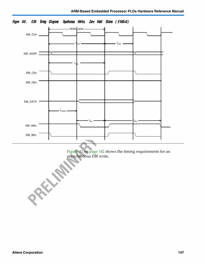
ARM-Based Embedded Processor PLDs Hardware Reference Manual
PRELIM
INARY IN
FORMAT
ION
Figure 40. EBI Timing Diagrams: Synchronous Write, Zero Wait States (EWS=0)
Figure 41 on page 142 shows the timing requirements for an asynchronous EBI write.
EBI_CLK
EBI_ADDR
EBI_CSn
EBI_OEn
EBI_DATA
EBI_WEn
Write_cycle
tWL tWH
tEAH
tCSL
tCSWH
tEAS
EBI_BEn
Altera Corporation 147
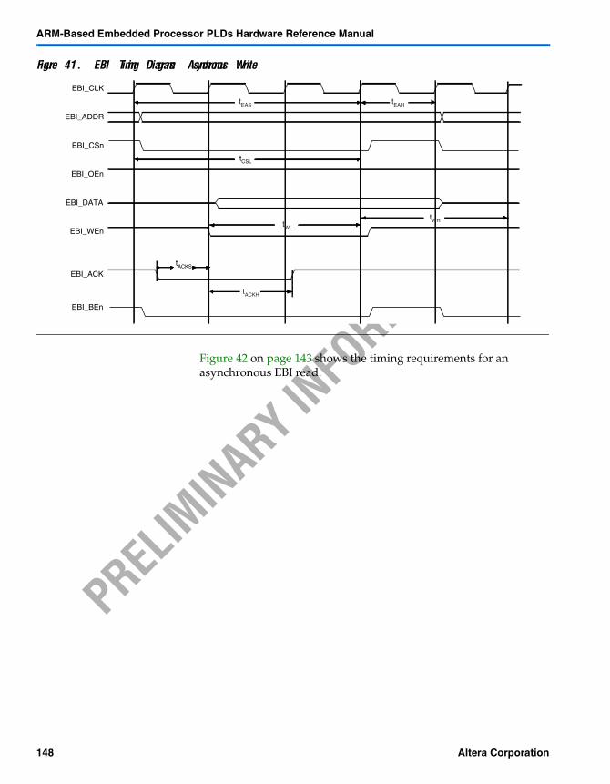
ARM-Based Embedded Processor PLDs Hardware Reference Manual
PRELIM
INARY IN
FORMAT
ION
Figure 41. EBI Timing Diagrams: Asynchronous Write
Figure 42 on page 143 shows the timing requirements for an asynchronous EBI read.
EBI_CLK
EBI_ADDR
EBI_CSn
EBI_OEn
EBI_DATA
EBI_WEn
EBI_ACKtACKS
tEAS tEAH
tCSL
tWHtWL
tACKH
EBI_BEn
148 Altera Corporation
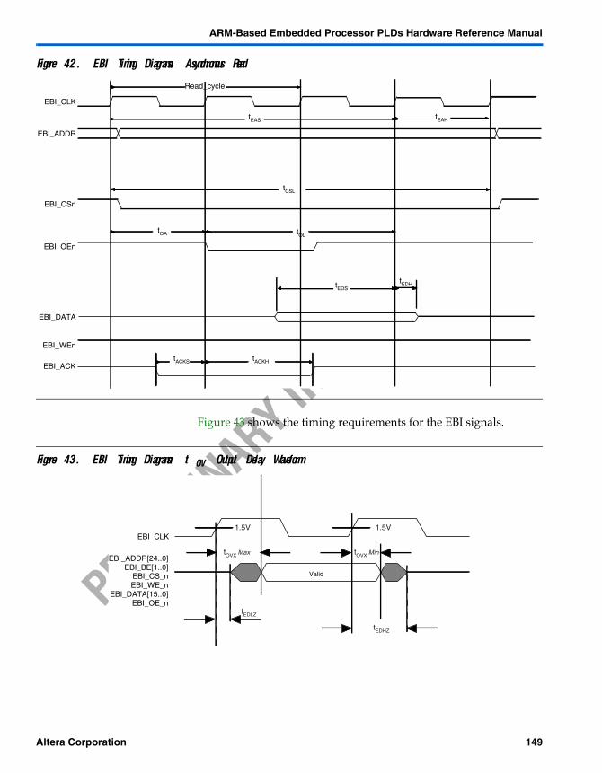
ARM-Based Embedded Processor PLDs Hardware Reference Manual
PRELIM
INARY IN
FORMAT
ION
Figure 42. EBI Timing Diagrams: Asynchronous Read
Figure 43 shows the timing requirements for the EBI signals.
Figure 43. EBI Timing Diagrams: tOV Output Delay Waveform
EBI_CLK
EBI_ADDR
EBI_CSn
EBI_OEn
EBI_DATA
EBI_WEn
tEDH
Read_cycle
tCSL
tOL
tEDS
tOA
tEAHtEAS
EBI_ACKtACKS tACKH
EBI_CLK1.5V 1.5V
tOVX Max tOVX Min
tEDLZ
tEDHZ
Valid
EBI_ADDR[24..0]EBI_BE[1..0]
EBI_CS_nEBI_WE_n
EBI_DATA[15..0]EBI_OE_n
Altera Corporation 149
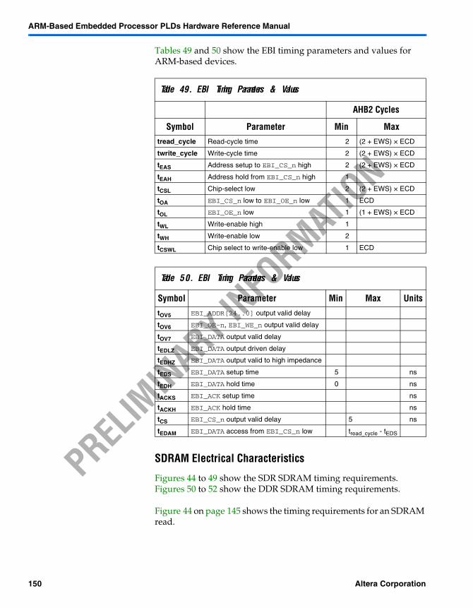
ARM-Based Embedded Processor PLDs Hardware Reference Manual
PRELIM
INARY IN
FORMAT
ION
Tables 49 and 50 show the EBI timing parameters and values for ARM-based devices.
SDRAM Electrical Characteristics
Figures 44 to 49 show the SDR SDRAM timing requirements. Figures 50 to 52 show the DDR SDRAM timing requirements.
Figure 44 on page 145 shows the timing requirements for an SDRAM read.
Table 49. EBI Timing Parameters & Values
AHB2 Cycles
Symbol Parameter Min Maxtread_cycle Read-cycle time 2 (2 + EWS) × ECD
twrite_cycle Write-cycle time 2 (2 + EWS) × ECD
tEAS Address setup to EBI_CS_n high 2 (2 + EWS) × ECD
tEAH Address hold from EBI_CS_n high 1
tCSL Chip-select low 2 (2 + EWS) × ECD
tOA EBI_CS_n low to EBI_OE_n low 1 ECD
tOL EBI_OE_n low 1 (1 + EWS) × ECD
tWL Write-enable high 1
tWH Write-enable low 2
tCSWL Chip select to write-enable low 1 ECD
Table 50. EBI Timing Parameters & Values
Symbol Parameter Min Max UnitstOV5 EBI_ADDR[24..0] output valid delay
tOV6 EBI_OE-n, EBI_WE_n output valid delay
tOV7 EBI_DATA output valid delay
tEDLZ EBI_DATA output driven delay
tEDHZ EBI_DATA output valid to high impedance
tEDS EBI_DATA setup time 5 ns
tEDH EBI_DATA hold time 0 ns
tACKS EBI_ACK setup time ns
tACKH EBI_ACK hold time ns
tCS EBI_CS_n output valid delay 5 ns
tEDAM EBI_DATA access from EBI_CS_n low tread_cycle - tEDS
150 Altera Corporation
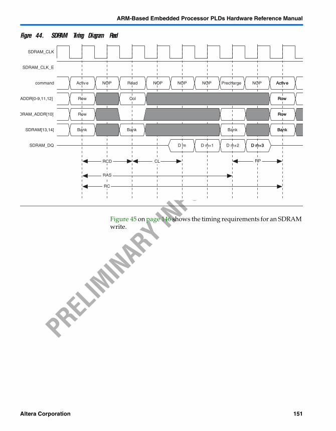
ARM-Based Embedded Processor PLDs Hardware Reference Manual
PRELIM
INARY IN
FORMAT
ION
Figure 44. SDRAM Timing Diagram: Read
Figure 45 on page 146 shows the timing requirements for an SDRAM write.
SDRAM_CLK
SDRAM_CLK_E
command
_ADDR[0-9,11,12]
DRAM_ADDR[10]
SDRAM[13,14]
SDRAM_DQ
Active NOP Read NOP NOP NOP Precharge NOP ActiveActive
Row Col RowRow
Row RowRow
Bank Bank Bank BankBank
D m D m+1 D m+2 D m+3D m+3
RCD CL RP
RAS
RC
Altera Corporation 151
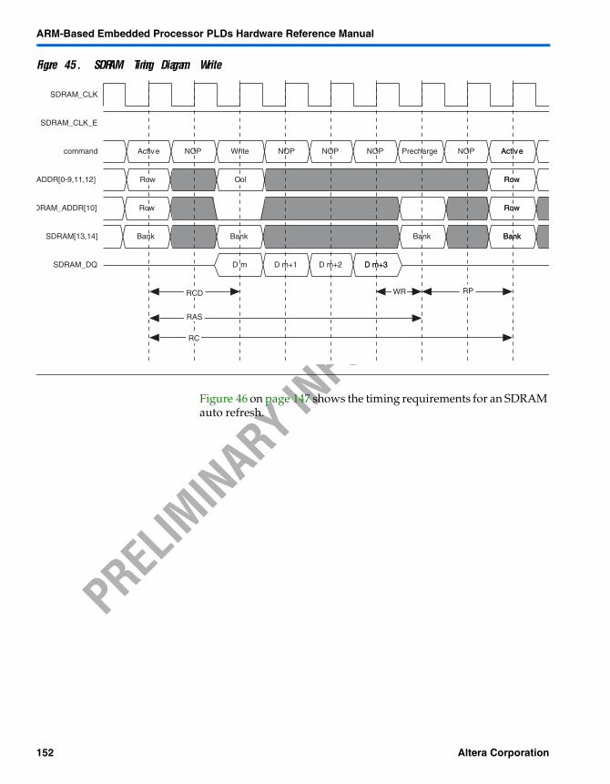
ARM-Based Embedded Processor PLDs Hardware Reference Manual
PRELIM
INARY IN
FORMAT
ION
Figure 45. SDRAM Timing Diagram: Write
Figure 46 on page 147 shows the timing requirements for an SDRAM auto refresh.
SDRAM_CLK
SDRAM_CLK_E
command
ADDR[0-9,11,12]
DRAM_ADDR[10]
SDRAM[13,14]
SDRAM_DQ
Active NOP Write NOP NOP NOP Precharge NOP ActiveActive
Row Col RowRow
Row RowRow
Bank Bank Bank BankBank
D m D m+1 D m+2 D m+3D m+3
RCD WR RP
RAS
RC
152 Altera Corporation
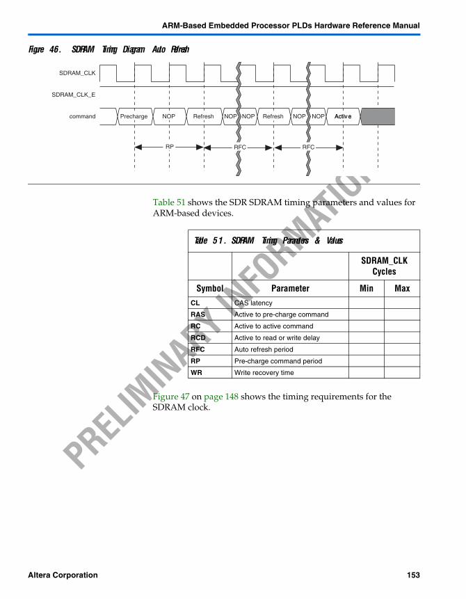
ARM-Based Embedded Processor PLDs Hardware Reference Manual
PRELIM
INARY IN
FORMAT
ION
Figure 46. SDRAM Timing Diagram: Auto Refresh
Table 51 shows the SDR SDRAM timing parameters and values for ARM-based devices.
Figure 47 on page 148 shows the timing requirements for the SDRAM clock.
SDRAM_CLK
SDRAM_CLK_E
command Precharge NOP Refresh NOP Refresh NOP ActiveActive
RP
NOP NOP
RFC RFC
Table 51. SDRAM Timing Parameters & Values
SDRAM_CLK Cycles
Symbol Parameter Min MaxCL CAS latency
RAS Active to pre-charge command
RC Active to active command
RCD Active to read or write delay
RFC Auto refresh period
RP Pre-charge command period
WR Write recovery time
Altera Corporation 153
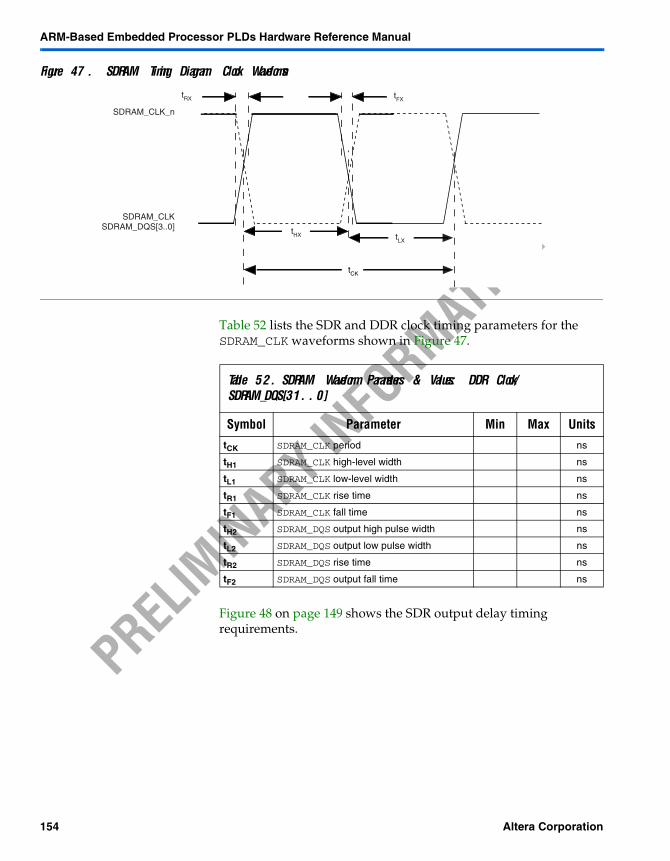
ARM-Based Embedded Processor PLDs Hardware Reference Manual
PRELIM
INARY IN
FORMAT
ION
Figure 47. SDRAM Timing Diagram: Clock Waveforms
Table 52 lists the SDR and DDR clock timing parameters for the SDRAM_CLK waveforms shown in Figure 47.
Figure 48 on page 149 shows the SDR output delay timing requirements.
tRX tFX
tHX tLX
tCK
SDRAM_CLK_n
SDRAM_CLKSDRAM_DQS[3..0]
Table 52. SDRAM Waveform Parameters & Values: DDR Clock/ SDRAM_DQS[31..0]
Symbol Parameter Min Max UnitstCK SDRAM_CLK period ns
tH1 SDRAM_CLK high-level width ns
tL1 SDRAM_CLK low-level width ns
tR1 SDRAM_CLK rise time ns
tF1 SDRAM_CLK fall time ns
tH2 SDRAM_DQS output high pulse width ns
tL2 SDRAM_DQS output low pulse width ns
tR2 SDRAM_DQS rise time ns
tF2 SDRAM_DQS output fall time ns
154 Altera Corporation
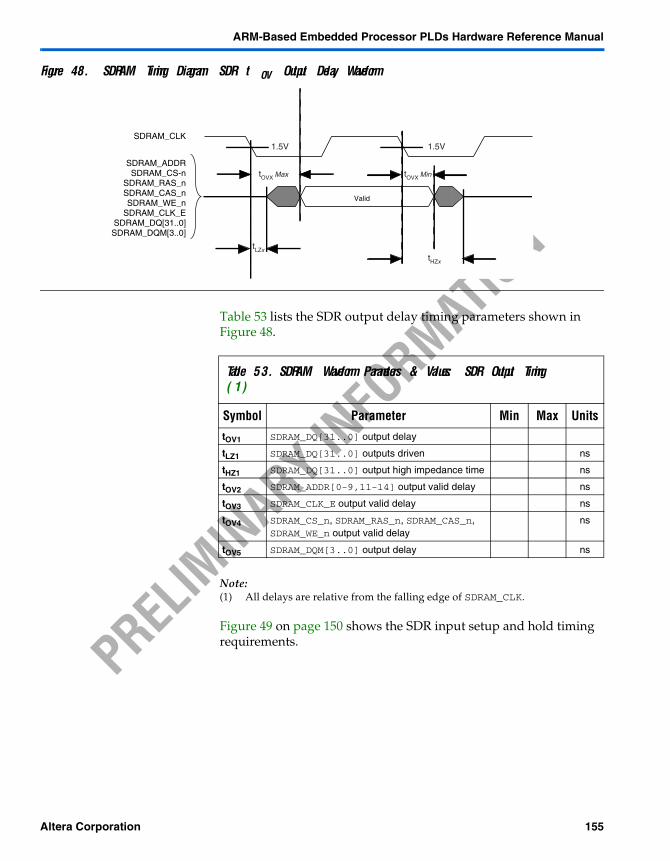
ARM-Based Embedded Processor PLDs Hardware Reference Manual
PRELIM
INARY IN
FORMAT
ION
Figure 48. SDRAM Timing Diagram: SDR tOV Output Delay Waveform
Table 53 lists the SDR output delay timing parameters shown in Figure 48.
Note:(1) All delays are relative from the falling edge of SDRAM_CLK.
Figure 49 on page 150 shows the SDR input setup and hold timing requirements.
SDRAM_CLK1.5V 1.5V
tOVX Max tOVX Min
tLZx
tHZx
Valid
SDRAM_ADDRSDRAM_CS-n
SDRAM_RAS_nSDRAM_CAS_nSDRAM_WE_n
SDRAM_CLK_ESDRAM_DQ[31..0]SDRAM_DQM[3..0]
Table 53. SDRAM Waveform Parameters & Values: SDR Output Timing (1)
Symbol Parameter Min Max UnitstOV1 SDRAM_DQ[31..0] output delay
tLZ1 SDRAM_DQ[31..0] outputs driven ns
tHZ1 SDRAM_DQ[31..0] output high impedance time ns
tOV2 SDRAM_ADDR[0-9,11-14] output valid delay ns
tOV3 SDRAM_CLK_E output valid delay ns
tOV4 SDRAM_CS_n, SDRAM_RAS_n, SDRAM_CAS_n, SDRAM_WE_n output valid delay
ns
tOV5 SDRAM_DQM[3..0] output delay ns
Altera Corporation 155
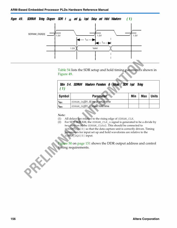
ARM-Based Embedded Processor PLDs Hardware Reference Manual
PRELIM
INARY IN
FORMAT
ION
Figure 49. SDRAM Timing Diagram: SDR tIS and tIH Input Setup and Hold Waveform (1)
Table 54 lists the SDR setup and hold timing parameters shown in Figure 49.
Note:(1) All delays are relative to the rising edge of SDRAM_CLK.(2) For SDR SDRAM, the SDRAM_CLK_n signal is generated to be a divide by
two version of the SDRAM_CLKx2. This should be connected to SDRAM_DQS[0] so that the data capture unit is correctly driven. Timing parameters for input set up and hold waveforms are relative to the SDRAM_DQS[0] input.
Figure 50 on page 151 shows the DDR output address and control timing requirements.
SDRAM_DQS[0]1.5V 1.5V 1.5V
tISX
tIHX
1.5V Valid
Table 54. SDRAM Waveform Parameters & Values: SDR Input Timing (1)
Symbol Parameter Min Max UnitstIS1 SDRAM_DQ[31..0] input setup time
tIH1 SDRAM_DQ[31..0] input hold time
156 Altera Corporation
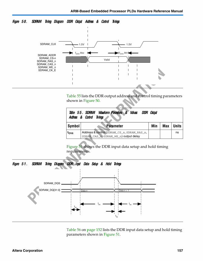
ARM-Based Embedded Processor PLDs Hardware Reference Manual
PRELIM
INARY IN
FORMAT
ION
Figure 50. SDRAM Timing Diagram: DDR Output Address & Control Timings
Table 55 lists the DDR output address and control timing parameters shown in Figure 50.
Figure 51 shows the DDR input data setup and hold timing requirements.
Figure 51. SDRAM Timing Diagram: DDR Input Data Setup & Hold Timings
Table 56 on page 152 lists the DDR input data setup and hold timing parameters shown in Figure 51.
SDRAM_CLK
SDRAM_ADDRSDRAM_CS-n
SDRAM_RAS_nSDRAM_CAS_nSDRAM_WE_nSDRAM_CK_E
1.5V 1.5V
tOVX Max tOVX Min
Valid
Table 55. SDRAM Waveform Parameters & Values: DDR Output Address & Control Timings
Symbol Parameter Min Max UnitstOV6 Address & control (SDRAM_CS_n, SDRAM_RAS_n,
SDRAM_CAS_n, SDRAM_WE_n) output delayns
SDRAM_DQS
SDRAM_DQ[31:0]
tIH tIHtIS
tIS
Data n Data n + 1
Altera Corporation 157
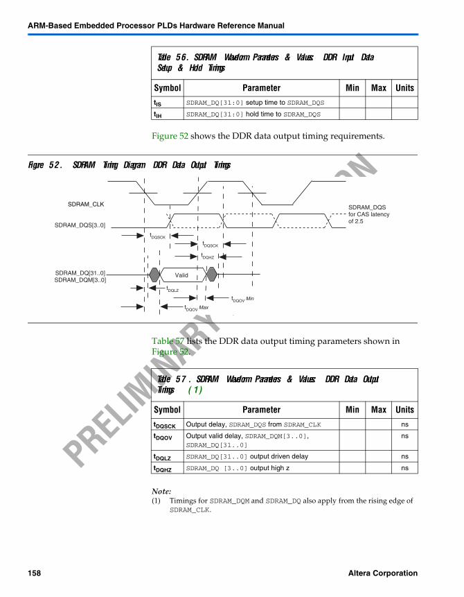
ARM-Based Embedded Processor PLDs Hardware Reference Manual
PRELIM
INARY IN
FORMAT
ION
Figure 52 shows the DDR data output timing requirements.
Figure 52. SDRAM Timing Diagram: DDR Data Output Timings
Table 57 lists the DDR data output timing parameters shown in Figure 52.
Note:(1) Timings for SDRAM_DQM and SDRAM_DQ also apply from the rising edge of
SDRAM_CLK.
Table 56. SDRAM Waveform Parameters & Values: DDR Input Data Setup & Hold Timings
Symbol Parameter Min Max UnitstIS SDRAM_DQ[31:0] setup time to SDRAM_DQS
tIH SDRAM_DQ[31:0] hold time to SDRAM_DQS
SDRAM_CLK
tDQSCK
tDQSCK
tDQLZ
tDQOV Max
tDQOV Min
SDRAM_DQ[31..0]SDRAM_DQM[3..0]
tDQHZ
Valid
SDRAM_DQS[3..0]
SDRAM_DQS for CAS latency of 2.5
Table 57. SDRAM Waveform Parameters & Values: DDR Data Output Timings (1)
Symbol Parameter Min Max Units
tDQSCK Output delay, SDRAM_DQS from SDRAM_CLK ns
tDQOV Output valid delay, SDRAM_DQM[3..0], SDRAM_DQ[31..0]
ns
tDQLZ SDRAM_DQ[31..0] output driven delay ns
tDQHZ SDRAM_DQ [3..0] output high z ns
158 Altera Corporation
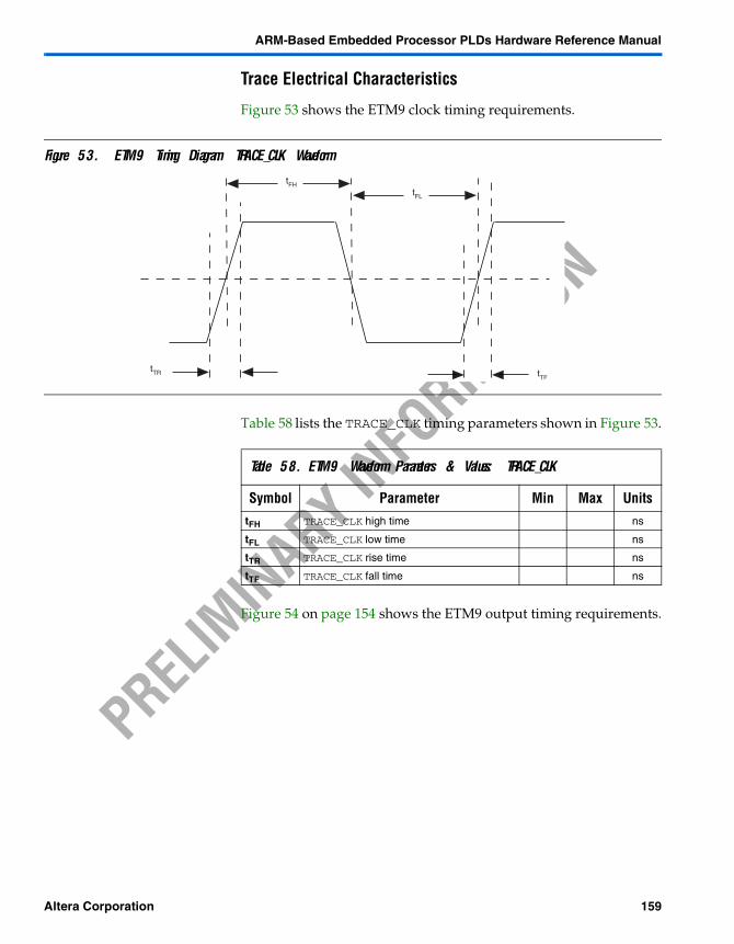
ARM-Based Embedded Processor PLDs Hardware Reference Manual
PRELIM
INARY IN
FORMAT
ION
Trace Electrical Characteristics
Figure 53 shows the ETM9 clock timing requirements.
Figure 53. ETM9 Timing Diagram: TRACE_CLK Waveform
Table 58 lists the TRACE_CLK timing parameters shown in Figure 53.
Figure 54 on page 154 shows the ETM9 output timing requirements.
tTR tTF
tFHtFL
Table 58. ETM9 Waveform Parameters & Values: TRACE_CLK
Symbol Parameter Min Max UnitstFH TRACE_CLK high time ns
tFL TRACE_CLK low time ns
tTR TRACE_CLK rise time ns
tTF TRACE_CLK fall time ns
Altera Corporation 159
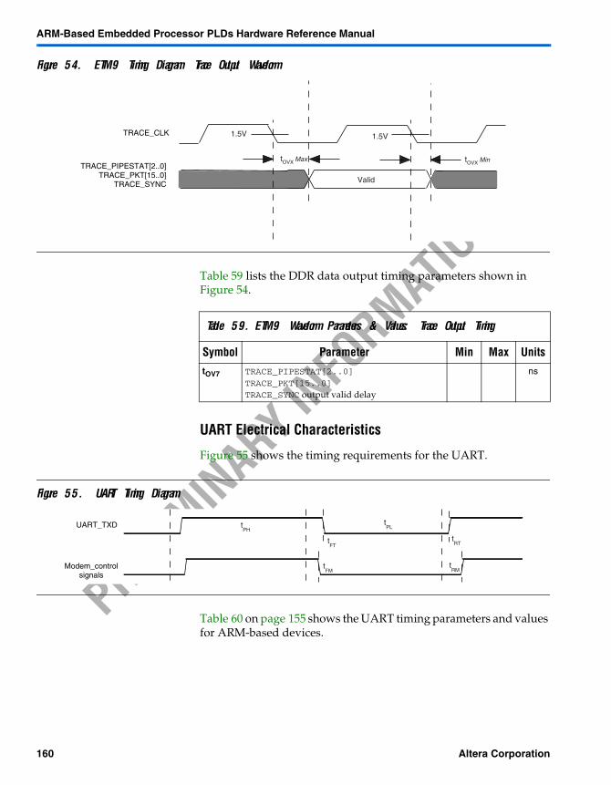
ARM-Based Embedded Processor PLDs Hardware Reference Manual
PRELIM
INARY IN
FORMAT
ION
Figure 54. ETM9 Timing Diagram: Trace Output Waveform
Table 59 lists the DDR data output timing parameters shown in Figure 54.
UART Electrical Characteristics
Figure 55 shows the timing requirements for the UART.
Figure 55. UART Timing Diagram
Table 60 on page 155 shows the UART timing parameters and values for ARM-based devices.
TRACE_CLK
TRACE_PIPESTAT[2..0]TRACE_PKT[15..0]
TRACE_SYNC
1.5V 1.5V
tOVX Max tOVX Min
Valid
Table 59. ETM9 Waveform Parameters & Values: Trace Output Timing
Symbol Parameter Min Max UnitstOV7 TRACE_PIPESTAT[2..0]
TRACE_PKT[15..0]TRACE_SYNC output valid delay
ns
UART_TXD
Modem_controlsignals
tFT
tRT
tPH
tPL
tFM
tRM
160 Altera Corporation
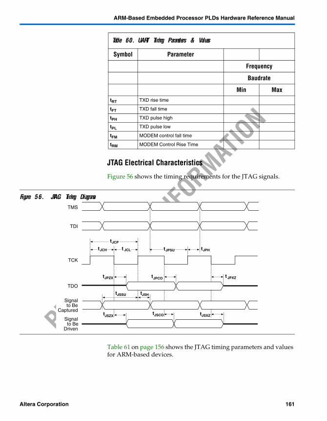
ARM-Based Embedded Processor PLDs Hardware Reference Manual
PRELIM
INARY IN
FORMAT
ION
JTAG Electrical Characteristics
Figure 56 shows the timing requirements for the JTAG signals.
Figure 56. JTAG Timing Diagrams
Table 61 on page 156 shows the JTAG timing parameters and values for ARM-based devices.
Table 60. UART Timing Parameters & Values
Symbol Parameter
Frequency
Baudrate
Min MaxtRT TXD rise time
tFT TXD fall time
tPH TXD pulse high
tPL TXD pulse low
tFM MODEM control fall time
tRM MODEM Control Rise Time
TDO
TCK
tJPZX tJPCO
tJPH
t JPXZ
tJCP
tJPSU t JCL tJCH
TDI
TMS
Signalto Be
Captured
Signalto Be
Driven
tJSZX
tJSSU tJSH
tJSCO tJSXZ
Altera Corporation 161
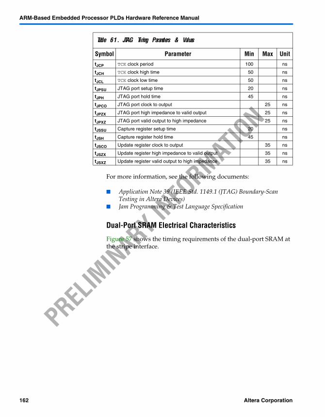
ARM-Based Embedded Processor PLDs Hardware Reference Manual
PRELIM
INARY IN
FORMAT
ION
For more information, see the following documents:
Application Note 39 (IEEE Std. 1149.1 (JTAG) Boundary-Scan Testing in Altera Devices)
Jam Programming & Test Language Specification
Dual-Port SRAM Electrical Characteristics
Figure 57 shows the timing requirements of the dual-port SRAM at the stripe interface.
Table 61. JTAG Timing Parameters & Values
Symbol Parameter Min Max Unit
tJCP TCK clock period 100 ns
tJCH TCK clock high time 50 ns
tJCL TCK clock low time 50 ns
tJPSU JTAG port setup time 20 ns
tJPH JTAG port hold time 45 ns
tJPCO JTAG port clock to output 25 ns
tJPZX JTAG port high impedance to valid output 25 ns
tJPXZ JTAG port valid output to high impedance 25 ns
tJSSU Capture register setup time 20 ns
tJSH Capture register hold time 45 ns
tJSCO Update register clock to output 35 ns
tJSZX Update register high impedance to valid output 35 ns
tJSXZ Update register valid output to high impedance 35 ns
162 Altera Corporation
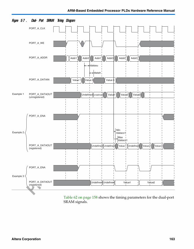
ARM-Based Embedded Processor PLDs Hardware Reference Manual
PRELIM
INARY IN
FORMAT
ION
Figure 57. Dual-Port SRAM Timing Diagram
Table 62 on page 158 shows the timing parameters for the dual-port SRAM signals.
PORT_A_CLK
PORT_A_WE
PORT_A_ADDR
PORT_A_DATAIN
PORT_A_DATAOUT(unregistered)
PORT_A_ENA
PORT_A_DATAOUT(registered)
PORT_A_ENA
PORT_A_DATAOUT(registered)
’h Addr 1 ’h6 Addr 2 Addr 1 Addr 3 Addr 2 Addr 3
Value 1 Value 2 Value 3
Undefined Undefined Value 1 Value 2 Value 3
Undefined Undefined Value 1 Undefined Value 2 Value 3
Undefined Undefined Value 1 Value 2
tdatasu
tdatah
Mintdataco1
Maxtdataco1
Example 1
Example 2
Example 3
Altera Corporation 163
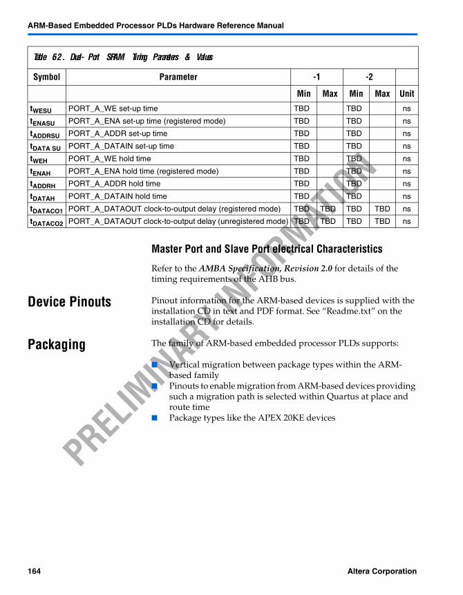
ARM-Based Embedded Processor PLDs Hardware Reference Manual
PRELIM
INARY IN
FORMAT
ION
Master Port and Slave Port electrical Characteristics
Refer to the AMBA Specification, Revision 2.0 for details of the timing requirements of the AHB bus.
Device Pinouts Pinout information for the ARM-based devices is supplied with the installation CD in text and PDF format. See “Readme.txt” on the installation CD for details.
Packaging The family of ARM-based embedded processor PLDs supports:
Vertical migration between package types within the ARM-based family
Pinouts to enable migration from ARM-based devices providing such a migration path is selected within Quartus at place and route time
Package types like the APEX 20KE devices
Table 62. Dual-Port SRAM Timing Parameters & Values
Symbol Parameter -1 -2
Min Max Min Max Unit
tWESU PORT_A_WE set-up time TBD TBD ns
tENASU PORT_A_ENA set-up time (registered mode) TBD TBD ns
tADDRSU PORT_A_ADDR set-up time TBD TBD ns
tDATA SU PORT_A_DATAIN set-up time TBD TBD ns
tWEH PORT_A_WE hold time TBD TBD ns
tENAH PORT_A_ENA hold time (registered mode) TBD TBD ns
tADDRH PORT_A_ADDR hold time TBD TBD ns
tDATAH PORT_A_DATAIN hold time TBD TBD ns
tDATACO1 PORT_A_DATAOUT clock-to-output delay (registered mode) TBD TBD TBD TBD ns
tDATACO2 PORT_A_DATAOUT clock-to-output delay (unregistered mode) TBD TBD TBD TBD ns
164 Altera Corporation
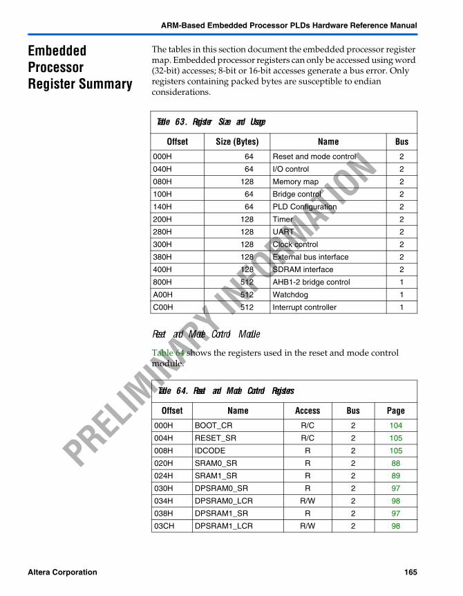
ARM-Based Embedded Processor PLDs Hardware Reference Manual
PRELIM
INARY IN
FORMAT
ION
Embedded Processor Register Summary
The tables in this section document the embedded processor register map. Embedded processor registers can only be accessed using word (32-bit) accesses; 8-bit or 16-bit accesses generate a bus error. Only registers containing packed bytes are susceptible to endian considerations.
Reset and Mode Control Module
Table 64 shows the registers used in the reset and mode control module.
Table 63. Register Size and Usage
Offset Size (Bytes) Name Bus
000H 64 Reset and mode control 2
040H 64 I/O control 2
080H 128 Memory map 2
100H 64 Bridge control 2
140H 64 PLD Configuration 2
200H 128 Timer 2
280H 128 UART 2
300H 128 Clock control 2
380H 128 External bus interface 2
400H 128 SDRAM interface 2
800H 512 AHB1-2 bridge control 1
A00H 512 Watchdog 1
C00H 512 Interrupt controller 1
Table 64. Reset and Mode Control Registers
Offset Name Access Bus Page
000H BOOT_CR R/C 2 104
004H RESET_SR R/C 2 105
008H IDCODE R 2 105
020H SRAM0_SR R 2 88
024H SRAM1_SR R 2 89
030H DPSRAM0_SR R 2 97
034H DPSRAM0_LCR R/W 2 98
038H DPSRAM1_SR R 2 97
03CH DPSRAM1_LCR R/W 2 98
Altera Corporation 165
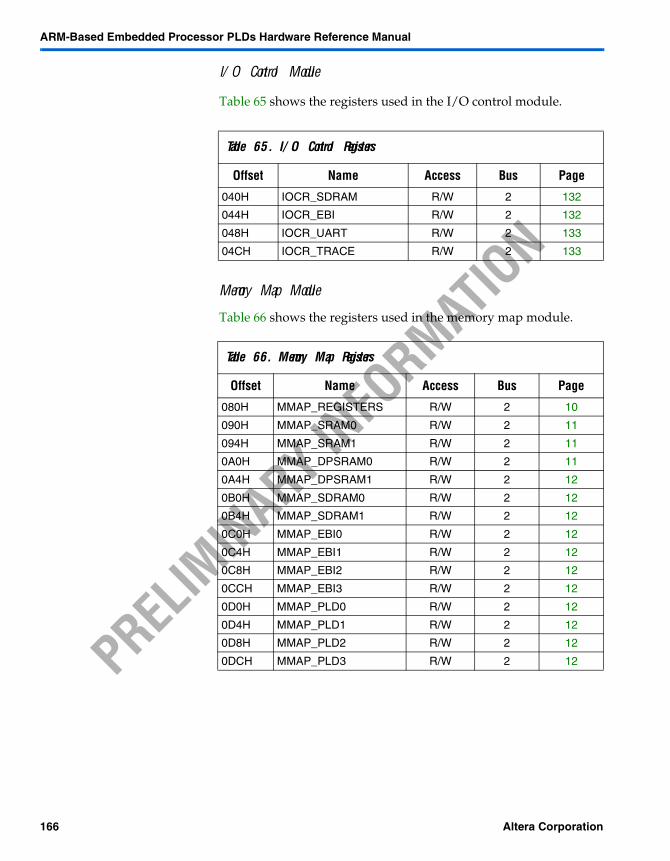
ARM-Based Embedded Processor PLDs Hardware Reference Manual
PRELIM
INARY IN
FORMAT
ION
I/O Control Module
Table 65 shows the registers used in the I/O control module.
Memory Map Module
Table 66 shows the registers used in the memory map module.
Table 65. I/O Control Registers
Offset Name Access Bus Page
040H IOCR_SDRAM R/W 2 132
044H IOCR_EBI R/W 2 132
048H IOCR_UART R/W 2 133
04CH IOCR_TRACE R/W 2 133
Table 66. Memory Map Registers
Offset Name Access Bus Page
080H MMAP_REGISTERS R/W 2 10
090H MMAP_SRAM0 R/W 2 11
094H MMAP_SRAM1 R/W 2 11
0A0H MMAP_DPSRAM0 R/W 2 11
0A4H MMAP_DPSRAM1 R/W 2 12
0B0H MMAP_SDRAM0 R/W 2 12
0B4H MMAP_SDRAM1 R/W 2 12
0C0H MMAP_EBI0 R/W 2 12
0C4H MMAP_EBI1 R/W 2 12
0C8H MMAP_EBI2 R/W 2 12
0CCH MMAP_EBI3 R/W 2 12
0D0H MMAP_PLD0 R/W 2 12
0D4H MMAP_PLD1 R/W 2 12
0D8H MMAP_PLD2 R/W 2 12
0DCH MMAP_PLD3 R/W 2 12
166 Altera Corporation
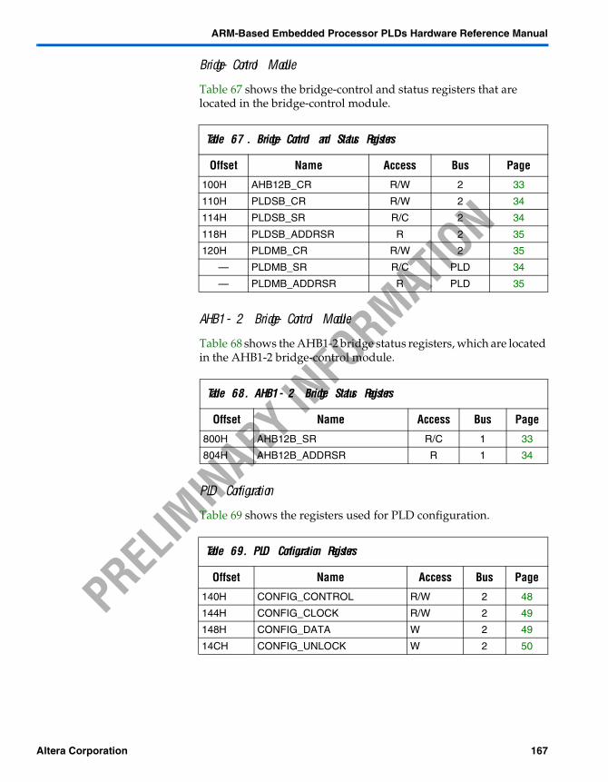
ARM-Based Embedded Processor PLDs Hardware Reference Manual
PRELIM
INARY IN
FORMAT
ION
Bridge-Control Module
Table 67 shows the bridge-control and status registers that are located in the bridge-control module.
AHB1-2 Bridge-Control Module
Table 68 shows the AHB1-2 bridge status registers, which are located in the AHB1-2 bridge-control module.
PLD Configuration
Table 69 shows the registers used for PLD configuration.
Table 67. Bridge-Control and Status Registers
Offset Name Access Bus Page
100H AHB12B_CR R/W 2 33
110H PLDSB_CR R/W 2 34
114H PLDSB_SR R/C 2 34
118H PLDSB_ADDRSR R 2 35
120H PLDMB_CR R/W 2 35
— PLDMB_SR R/C PLD 34
— PLDMB_ADDRSR R PLD 35
Table 68. AHB1-2 Bridge Status Registers
Offset Name Access Bus Page
800H AHB12B_SR R/C 1 33
804H AHB12B_ADDRSR R 1 34
Table 69. PLD Configuration Registers
Offset Name Access Bus Page
140H CONFIG_CONTROL R/W 2 48
144H CONFIG_CLOCK R/W 2 49
148H CONFIG_DATA W 2 49
14CH CONFIG_UNLOCK W 2 50
Altera Corporation 167
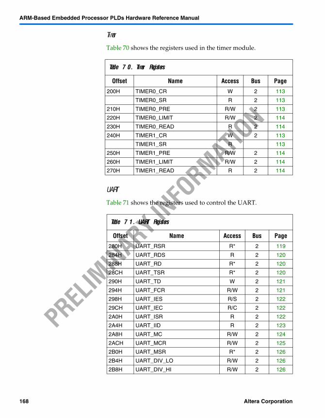
ARM-Based Embedded Processor PLDs Hardware Reference Manual
PRELIM
INARY IN
FORMAT
ION
Timer
Table 70 shows the registers used in the timer module.
UART
Table 71 shows the registers used to control the UART.
Table 70. Timer Registers
Offset Name Access Bus Page
200H TIMER0_CR W 2 113
TIMER0_SR R 2 113
210H TIMER0_PRE R/W 2 113
220H TIMER0_LIMIT R/W 2 114
230H TIMER0_READ R 2 114
240H TIMER1_CR W 2 113
TIMER1_SR R 113
250H TIMER1_PRE R/W 2 114
260H TIMER1_LIMIT R/W 2 114
270H TIMER1_READ R 2 114
Table 71. UART Registers
Offset Name Access Bus Page
280H UART_RSR R* 2 119
284H UART_RDS R 2 120
288H UART_RD R* 2 120
28CH UART_TSR R* 2 120
290H UART_TD W 2 121
294H UART_FCR R/W 2 121
298H UART_IES R/S 2 122
29CH UART_IEC R/C 2 122
2A0H UART_ISR R 2 122
2A4H UART_IID R 2 123
2A8H UART_MC R/W 2 124
2ACH UART_MCR R/W 2 125
2B0H UART_MSR R* 2 126
2B4H UART_DIV_LO R/W 2 126
2B8H UART_DIV_HI R/W 2 126
168 Altera Corporation
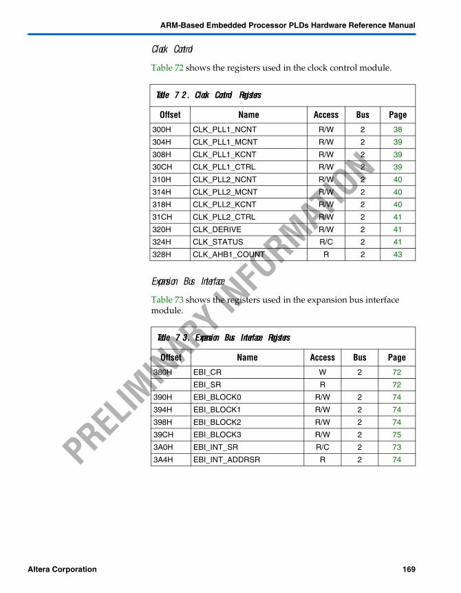
ARM-Based Embedded Processor PLDs Hardware Reference Manual
PRELIM
INARY IN
FORMAT
ION
Clock Control
Table 72 shows the registers used in the clock control module.
Expansion Bus Interface
Table 73 shows the registers used in the expansion bus interface module.
Table 72. Clock Control Registers
Offset Name Access Bus Page
300H CLK_PLL1_NCNT R/W 2 38
304H CLK_PLL1_MCNT R/W 2 39
308H CLK_PLL1_KCNT R/W 2 39
30CH CLK_PLL1_CTRL R/W 2 39
310H CLK_PLL2_NCNT R/W 2 40
314H CLK_PLL2_MCNT R/W 2 40
318H CLK_PLL2_KCNT R/W 2 40
31CH CLK_PLL2_CTRL R/W 2 41
320H CLK_DERIVE R/W 2 41
324H CLK_STATUS R/C 2 41
328H CLK_AHB1_COUNT R 2 43
Table 73. Expansion Bus Interface Registers
Offset Name Access Bus Page
380H EBI_CR W 2 72
EBI_SR R 72
390H EBI_BLOCK0 R/W 2 74
394H EBI_BLOCK1 R/W 2 74
398H EBI_BLOCK2 R/W 2 74
39CH EBI_BLOCK3 R/W 2 75
3A0H EBI_INT_SR R/C 2 73
3A4H EBI_INT_ADDRSR R 2 74
Altera Corporation 169
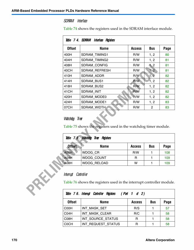
ARM-Based Embedded Processor PLDs Hardware Reference Manual
PRELIM
INARY IN
FORMAT
ION
SDRAM Interface
Table 74 shows the registers used in the SDRAM interface module.
Watchdog Timer
Table 75 shows the registers used in the watchdog timer module.
Interrupt Controller
Table 76 shows the registers used in the interrupt controller module.
Table 74. SDRAM Interface Registers
Offset Name Access Bus Page
400H SDRAM_TIMING1 R/W 1, 2 80
404H SDRAM_TIMING2 R/W 1, 2 81
408H SDRAM_CONFIG R/W 1, 2 81
40CH SDRAM_REFRESH R/W 1, 2 81
410H SDRAM_ADDR R/W 1, 2 82
414H SDRAM_BUS1 R/W 1, 2 82
418H SDRAM_BUS2 R/W 1, 2 82
41CH SDRAM_INIT R/W 1, 2 82
420H SDRAM_MODE0 R/W 1, 2 82
424H SDRAM_MODE1 R/W 1, 2 83
07CH SDRAM_WIDTH R/W 2 83
Table 75. Watchdog Timer Registers
Offset Name Access Bus Page
A00H WDOG_CR R/W 1 108
A04H WDOG_COUNT R 1 109
A08H WDOG_RELOAD W 1 109
Table 76. Interrupt Controller Registers (Part 1 of 2)
Offset Name Access Bus Page
C00H INT_MASK_SET R/S 1 57
C04H INT_MASK_CLEAR R/C 1 58
C08H INT_SOURCE_STATUS R 1 58
C0CH INT_REQUEST_STATUS R 1 58
170 Altera Corporation
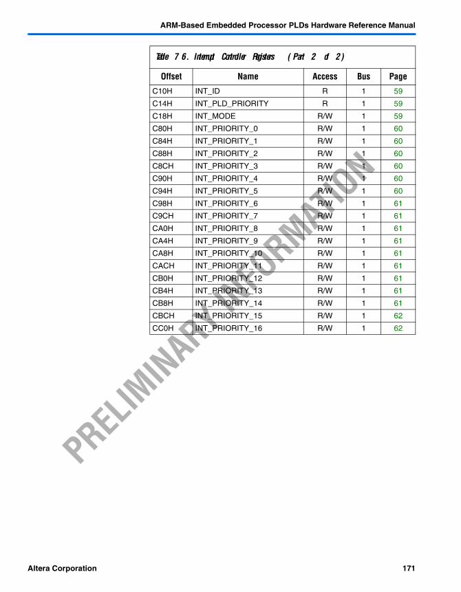
ARM-Based Embedded Processor PLDs Hardware Reference Manual
PRELIM
INARY IN
FORMAT
ION
C10H INT_ID R 1 59
C14H INT_PLD_PRIORITY R 1 59
C18H INT_MODE R/W 1 59
C80H INT_PRIORITY_0 R/W 1 60
C84H INT_PRIORITY_1 R/W 1 60
C88H INT_PRIORITY_2 R/W 1 60
C8CH INT_PRIORITY_3 R/W 1 60
C90H INT_PRIORITY_4 R/W 1 60
C94H INT_PRIORITY_5 R/W 1 60
C98H INT_PRIORITY_6 R/W 1 61
C9CH INT_PRIORITY_7 R/W 1 61
CA0H INT_PRIORITY_8 R/W 1 61
CA4H INT_PRIORITY_9 R/W 1 61
CA8H INT_PRIORITY_10 R/W 1 61
CACH INT_PRIORITY_11 R/W 1 61
CB0H INT_PRIORITY_12 R/W 1 61
CB4H INT_PRIORITY_13 R/W 1 61
CB8H INT_PRIORITY_14 R/W 1 61
CBCH INT_PRIORITY_15 R/W 1 62
CC0H INT_PRIORITY_16 R/W 1 62
Table 76. Interrupt Controller Registers (Part 2 of 2)
Offset Name Access Bus Page
Altera Corporation 171
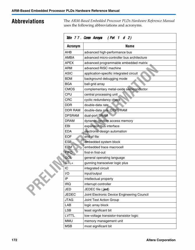
ARM-Based Embedded Processor PLDs Hardware Reference Manual
PRELIM
INARY IN
FORMAT
ION
Abbreviations The ARM-Based Embedded Processor PLDs Hardware Reference Manual uses the following abbreviations and acronyms.
Table 77. Common Acronyms (Part 1 of 2)
Acronym Name
AHB advanced high-performance bus
AMBA advanced micro-controller bus architecture
APEX advanced programmable embedded matrix
ARM advanced RISC machine
ASIC application-specific integrated circuit
BDM background debugging mode
BGA ball-grid array
CMOS complementary metal-oxide semiconductor
CPU central processing unit
CRC cyclic redundancy check
DDR double-data rate
DDR RAM double-data rate (DDR) RAM
DPSRAM dual-port SRAM
DRAM dynamic random access memory
EBI expansion bus interface
EDA electronic-design automation
EOF end of file
ESB embedded system block
ETM embedded trace macrocell
FIFO first-in first-out
GOL general operating language
GTL+ gunning transceiver logic plus
IC integrated circuit
I/O input/output
IP intellectual property
IRQ interrupt controller
JED JEDEC file (.jed)
JEDEC Joint Electronic Device Engineering Council
JTAG Joint Test Action Group
LAB logic array block
LSB least significant bit
LVTTL low-voltage transistor-transistor logic
MMU memory management unit
MSB most significant bit
172 Altera Corporation
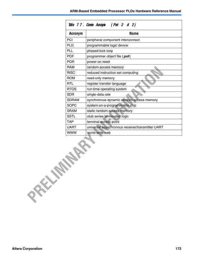
ARM-Based Embedded Processor PLDs Hardware Reference Manual
PRELIM
INARY IN
FORMAT
ION
PCI peripheral component interconnect
PLD programmable logic device
PLL phased-lock loop
POF programmer object file (.pof)
POR power-on reset
RAM random-access memory
RISC reduced instruction set computing
ROM read-only memory
RTL register transfer language
RTOS run-time operating system
SDR single-data rate
SDRAM synchronous dynamic random-access memory
SOPC system-on-a-programmable chip
SRAM static random access memory
SSTL stub series terminated logic
TAP terminal access point
UART universal asynchronous receiver/transmitter UART
WWW world-wide web
Table 77. Common Acronyms (Part 2 of 2)
Acronym Name
Altera Corporation 173
ARM-Based Embedded Processor PLDs Hardware Reference Manual
PRELIM
INARY IN
FORMAT
ION
Glossary A
APEX 20K An Altera embedded programmable logic device family based on the Advanced Programmable Embedded Matrix (APEXTM) architecture, which integrates look-up table logic, product-term logic, and memory in a single device. This family offers complete system integration on a single device. The APEX 20K device family includes the EP20K100, EP20K100E, EP20K160E, EP20K200, EP20K200E, EP20K300E, EP20K400, EP20K400E, EP20K600E, and EP20K1000E devices.
B
ball-grid array (BGA) A high-performance device package offered by Altera that allows for higher pin counts in significantly less board area than quad flat pack (QFP) packages and have better thermal characteristics than most QFP packages. BGA packages are rapidly becoming the preferred packages for high-density PLDs. See the Altera Device Package Information Data Sheet and Ordering Information for more information.
beat .A movement of data in a single clock period, which could be a byte, a half-word (2 bytes) or a word (4 bytes). Thus a burst transaction with 4 beats can be 4, 8 or 16 bytes, depending on the transaction size.
ByteBlasterMV cable A parallel download cable that allows PC users to program and configure devices in-system. The ByteBlasterMVTM parallel port download cable provides configuration support for APEX 20K, FLEX 10K, FLEX 8000, and FLEX 6000 devices. APEX 20K, FLEX 6000 and FLEX 10K devices can be configured together in a chain.
C
configuration device Altera’s family of serial devices, which are designed to configure APEX and FLEX devices. See the Configuration Devices for APEX & FLEX Devices Data Sheet for more information.
configuration scheme The method used to load data into APEX 20K and FLEX devices.
Five configuration schemes are available for APEX 20K and FLEX 10K devices: configuration device, passive serial (PS), passive parallel asynchronous (PPA), passive parallel synchronous (PPS), and IEEE Std. 1149.1 Joint Test Action Group (JTAG). For complete
174 Altera Corporation
ARM-Based Embedded Processor PLDs Hardware Reference Manual
PRELIM
INARY IN
FORMAT
ION
information on FLEX 10K configuration schemes, see Application Note 116 (Configuring APEX 20K, FLEX 10K, and FLEX 6000 Devices).
Three configuration schemes are available for FLEX 6000 devices: configuration device, passive serial (PS), and passive serial asynchronous (PSA). For complete information on FLEX 6000 configuration schemes, see Application Note 116 (Configuring APEX 20K, FLEX 10K, and FLEX 6000 Devices).
D
dedicated input pin A pin that can only be used as an input to the device.
device Refers to an Altera programmable logic device, including APEX 20K, FLEX 10K, FLEX 8000, FLEX 6000, MAX 9000, MAX 7000, MAX 3000A, MAX 5000, and Classic devices. Altera also offers configuration devices that are used to configure APEX 20K, FLEX 10K, FLEX 8000, and FLEX 6000 devices.
device family A group of Altera programmable logic devices with the same fundamental architecture. Altera device families include the APEX 20K, FLEX 10K, FLEX 8000, FLEX 6000, MAX 9000, MAX 7000, MAX 3000A, MAX 5000, and Classic device families. Altera also offers a configuration device family that includes devices used for configuring APEX 20K, FLEX 10K, FLEX 8000, and FLEX 6000 devices.
E
Embedded logic Logic that is implemented in the stripe.
EPXA Family signature on a part number that refers to the Excalibur ARM-based device families.
F
FineLine BGA FineLine BGATM packages available for ARM-based, APEX 20K, FLEX 10K, and MAX 7000 devices use only half the board area of traditional BGA packages and are offered with as many as 784 pins for the EP20K1000E device. This new package allows designs to be effectively implemented into higher density, higher pin count devices into designs while decreasing board space and costs. See the Altera Device Package Information Data Sheet and Ordering Information for more information.
Altera Corporation 175
ARM-Based Embedded Processor PLDs Hardware Reference Manual
PRELIM
INARY IN
FORMAT
ION
I
I/O cell Also known as an I/O element. A register that exists on the periphery of anAPEX 20K, FLEX 10K, FLEX 8000, or MAX 9000 device, or a fast input-type logic cell that is associated with an I/O pin in MAX 7000E, MAX 7000S, or MAX 7000A devices. I/O cells give short setup and clock-to-out times.
J
Joint Test Action Group (JTAG) A set of specifications that enables a designer to perform board- and device-level functional verification of a board during production.
JTAG boundary-scan testing Testing that isolates a device’s internal circuitry from its I/O circuitry. This testing is made possible by the JTAG boundary-scan test (BST) architecture that is available in all APEX 20K, FLEX 10K devices, all FLEX 8000 devices except the EPF8452A and EPF81188A, and all FLEX 6000, MAX 9000, MAX 7000S, MAX 7000A and MAX 3000A devices. Serial data is shifted into boundary-scan cells in the device; observed data is shifted out and externally compared to expected results. Boundary-scan testing offers efficient PC board testing, providing an electronic substitute for the traditional “bed of nails” test fixtures.
L
locked transaction A term used to qualify transactions (usually reads and writes) that take place without losing bus access. Masters request locked access to memory by asserting a lock signal at the same time as requesting the bus. In this situation, the bus remains granted to the master until the lock is de-asserted.
logic cell The generic term for the basic building block of an Altera device. In APEX 20K, FLEX 10K, FLEX 8000, and FLEX 6000 devices, logic cells are called logic elements. In MAX 9000, MAX 7000, MAX 3000A, MAX 5000, and Classic devices, logic cells are called macrocells.
logic element (LE) A basic building block of APEX 20K, FLEX 10K, FLEX 8000, and FLEX 6000 devices. A logic element consists of a look-up table (LUT)—i.e., a function generator that quickly computes any function of four variables—and a programmable register to support sequential functions. The register can be programmed as a flow-through latch, as a D, T, JK, or SR flipflop, or bypassed entirely for pure combinatorial logic. The register can feed
176 Altera Corporation
ARM-Based Embedded Processor PLDs Hardware Reference Manual
PRELIM
INARY IN
FORMAT
ION
other logic cells or feed back to the logic cell itself. Some logic elements feed output or bidirectional I/O pins on the device.
M
MasterBlaster Communications Cable The MasterBlasterTM
communications cable uses a PC serial or USB port hardware interface. This cable provides configuration data to APEX 20K, FLEX 10K, FLEX 8000, and FLEX 6000 devices, as well as programming data to MAX 9000, MAX 7000S, MAX 7000A, and MAX 3000A devices. The MasterBlaster communications cable also supports in-circuit debugging with the SignalTap embedded logic analyzer in APEX 20K devices.
P
plastic J-lead chip carrier (PLCC) A device package option offered by Altera. Both ceramic J-lead chip carrier (JLCC) and PLCC packages are available. See the Altera Device Package Information Data Sheet and Ordering Information for more information.
posted write A write that is posted to a bridge FIFO and usually acknowledged immediately. However, the write need not have occurred at the time of acknowledgement. It is queued before sending to the destination.
product term Two or more factors in a Boolean expression combined with an AND operator constitute a product term, where “product” means “logic product”.
programmable logic devices (PLDs) Digital, user-configurable integrated circuits used to implement custom logic functions. PLDs can implement any Boolean expression or registered function with built-in logic structures.
Q
Quartus The Quartus™ software is Altera’s fourth generation development system for programmable logic and allows designers to process multi-million gate designs. Features of the Quartus software include: work group computing, integrated logic analysis functionality, electronic design automation (EDA) tool integration, multi-processor support, incremental recompilation, and intellectual property (IP) integration.
Altera Corporation 177
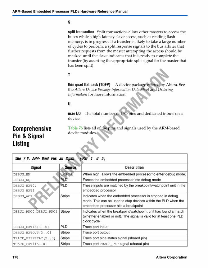
ARM-Based Embedded Processor PLDs Hardware Reference Manual
PRELIM
INARY IN
FORMAT
ION
S
split transaction Split transactions allow other masters to access the buses while a high-latency slave access, such as reading flash memory, is in progress. If a transfer is likely to take a large number of cycles to perform, a split response signals to the bus arbiter that further requests from the master attempting the access should be masked until the slave indicates that it is ready to complete the transfer (by asserting the appropriate split signal for the master that has been split)
T
thin quad flat pack (TQFP) A device package offered by Altera. See the Altera Device Package Information Data Sheet and Ordering Information for more information.
U
user I/O The total number of I/O pins and dedicated inputs on a device.
Comprehensive Pin & Signal Listing
Table 78 lists all of the pins and signals used by the ARM-based device modules.
Table 78. ARM-Based Pins and Signals (Part 1 of 5)
Signal Source Description
DEBUG_EN External When high, allows the embedded processor to enter debug mode.
DEBUG_RQ PLD Forces the embedded processor into debug mode
DEBUG_EXT0, DEBUG_EXT1
PLD These inputs are matched by the breakpoint/watchpoint unit in the embedded processor
DEBUG_ACK Stripe Indicates when the embedded processor is stopped in debug mode. This can be used to stop devices within the PLD when the embedded processor hits a breakpoint
DEBUG_RNG0, DEBUG_RNG1 Stripe Indicates when the breakpoint/watchpoint unit has found a match (whether enabled or not). The signal is valid for at least one PLD clock cycle
DEBUG_EXTIN[3..0] PLD Trace port input
DEBUG_EXTOUT[3..0] Stripe Trace port output
TRACE_PIPESTAT[2..0] Stripe Trace port pipe status signal (shared pin)
TRACE_PKT[15..0] Stripe Trace port TRACE_PKT signal (shared pin)
178 Altera Corporation
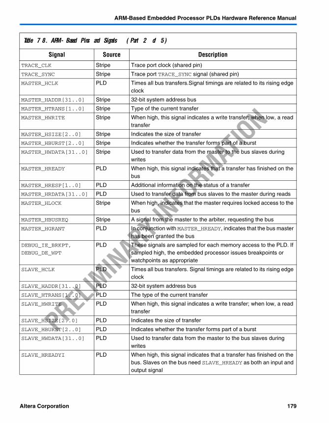
ARM-Based Embedded Processor PLDs Hardware Reference Manual
PRELIM
INARY IN
FORMAT
ION
TRACE_CLK Stripe Trace port clock (shared pin)
TRACE_SYNC Stripe Trace port TRACE_SYNC signal (shared pin)
MASTER_HCLK PLD Times all bus transfers.Signal timings are related to its rising edge clock
MASTER_HADDR[31..0] Stripe 32-bit system address bus
MASTER_HTRANS[1..0] Stripe Type of the current transfer
MASTER_HWRITE Stripe When high, this signal indicates a write transfer; when low, a read transfer
MASTER_HSIZE[2..0] Stripe Indicates the size of transfer
MASTER_HBURST[2..0] Stripe Indicates whether the transfer forms part of a burst
MASTER_HWDATA[31..0] Stripe Used to transfer data from the master to the bus slaves during writes
MASTER_HREADY PLD When high, this signal indicates that a transfer has finished on the bus
MASTER_HRESP[1..0] PLD Additional information on the status of a transfer
MASTER_HRDATA[31..0] PLD Used to transfer data from bus slaves to the master during reads
MASTER_HLOCK Stripe When high, indicates that the master requires locked access to the bus
MASTER_HBUSREQ Stripe A signal from the master to the arbiter, requesting the bus
MASTER_HGRANT PLD In conjunction with MASTER_HREADY, indicates that the bus master has been granted the bus
DEBUG_IE_BRKPT, DEBUG_DE_WPT
PLD These signals are sampled for each memory access to the PLD. If sampled high, the embedded processor issues breakpoints or watchpoints as appropriate
SLAVE_HCLK PLD Times all bus transfers. Signal timings are related to its rising edge clock
SLAVE_HADDR[31..0] PLD 32-bit system address bus
SLAVE_HTRANS[1..0] PLD The type of the current transfer
SLAVE_HWRITE PLD When high, this signal indicates a write transfer; when low, a read transfer
SLAVE_HSIZE[2..0] PLD Indicates the size of transfer
SLAVE_HBURST[2..0] PLD Indicates whether the transfer forms part of a burst
SLAVE_HWDATA[31..0] PLD Used to transfer data from the master to the bus slaves during writes
SLAVE_HREADYI PLD When high, this signal indicates that a transfer has finished on the bus. Slaves on the bus need SLAVE_HREADY as both an input and output signal
Table 78. ARM-Based Pins and Signals (Part 2 of 5)
Signal Source Description
Altera Corporation 179
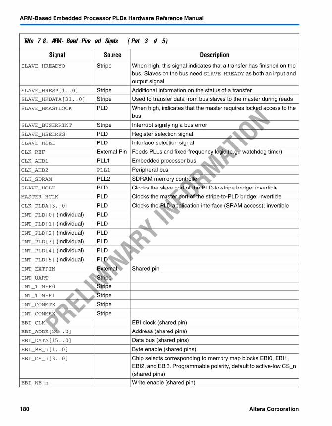
ARM-Based Embedded Processor PLDs Hardware Reference Manual
PRELIM
INARY IN
FORMAT
ION
SLAVE_HREADYO Stripe When high, this signal indicates that a transfer has finished on the bus. Slaves on the bus need SLAVE_HREADY as both an input and output signal
SLAVE_HRESP[1..0] Stripe Additional information on the status of a transfer
SLAVE_HRDATA[31..0] Stripe Used to transfer data from bus slaves to the master during reads
SLAVE_HMASTLOCK PLD When high, indicates that the master requires locked access to the bus
SLAVE_BUSERRINT Stripe Interrupt signifying a bus error
SLAVE_HSELREG PLD Register selection signal
SLAVE_HSEL PLD Interface selection signal
CLK_REF External Pin Feeds PLLs and fixed-frequency logic (e.g., watchdog timer)
CLK_AHB1 PLL1 Embedded processor bus
CLK_AHB2 PLL1 Peripheral bus
CLK_SDRAM PLL2 SDRAM memory controller
SLAVE_HCLK PLD Clocks the slave port of the PLD-to-stripe bridge; invertible
MASTER_HCLK PLD Clocks the master port of the stripe-to-PLD bridge; invertible
CLK_PLDA[3..0] PLD Clocks the PLD application interface (SRAM access); invertible
INT_PLD[0] (individual) PLD
INT_PLD[1] (individual) PLD
INT_PLD[2] (individual) PLD
INT_PLD[3] (individual) PLD
INT_PLD[4] (individual) PLD
INT_PLD[5] (individual) PLD
INT_EXTPIN External Shared pin
INT_UART Stripe
INT_TIMER0 Stripe
INT_TIMER1 Stripe
INT_COMMTX Stripe
INT_COMMRX Stripe
EBI_CLK EBI clock (shared pin)
EBI_ADDR[24..0] Address (shared pins)
EBI_DATA[15..0] Data bus (shared pins)
EBI_BE_n[1..0] Byte enable (shared pins)
EBI_CS_n[3..0] Chip selects corresponding to memory map blocks EBI0, EBI1, EBI2, and EBI3. Programmable polarity, default to active-low CS_n (shared pins)
EBI_WE_n Write enable (shared pin)
Table 78. ARM-Based Pins and Signals (Part 3 of 5)
Signal Source Description
180 Altera Corporation
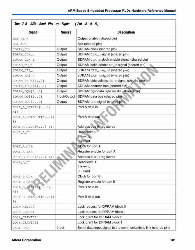
ARM-Based Embedded Processor PLDs Hardware Reference Manual
PRELIM
INARY IN
FORMAT
ION
EBI_OE_n Output enable (shared pin)
EBI_ACK Ack (shared pin)
SDRAM_CLK Output SDRAM clock (shared pin)
SDRAM_CLK_n Output SDRAM CLK_n signal (shared pin)
SDRAM_CLK_E Output SDRAM CLK_E clock enable signal (shared pin)
SDRAM_WE_n Output SDRAM write enable WE_n signal (shared pin)
SDRAM_CAS_n Output SDRAM CAS_n signal (shared pin)
SDRAM_RAS_n Output SDRAM RAS_n signal (shared pin)
SDRAM_CS_n[1..0] Output SDRAM chip selects CS_n signal (shared pin)
SDRAM_ADDR[14..0] Output SDRAM address bus (shared pin)
SDRAM_DQM[3..0] Output SDRAM DQM data byte masks (shared pin)
SDRAM_DQ[31..0] Input/Output SDRAM data bus (shared pin)
SDRAM_DQS[3..0] Output SDRAM DQS signal (shared pin)
PORT_A_DATAIN[n..0]
(1)
Port A data in
PORT_A_DATAOUT[n..0](
1)
Port A data out
PORT_A_ADDR[n..0] (1) Address bus 0; registered
PORT_A_WE Read/write 01 = write0 = read
PORT_A_CLK Clock for port A
PORT_A_ENA Register enable for port A
PORT_B_ADDR[n..0] (1) Address bus 1; registered
PORT_B_WE Read/write 11 = write0 = read
PORT_B_CLK Clock for port B
PORT_B_ENA Register enable for port B
PORT_B_DATAIN[n..0]
(1)
Port B data in
PORT_B_DATAOUT[n..0](
1)
Port B data out
LOCK_REQDP0 Lock request for DPRAM block 0
LOCK_REQDP1 Lock request for DPRAM block 1
LOCK_GRANTDP0 Lock grant for DPRAM block 0
LOCK_GRANTDP1 Lock grant for DPRAM block 1
UART_RXD Input Serial data input signal to the communications link (shared pin)
Table 78. ARM-Based Pins and Signals (Part 4 of 5)
Signal Source Description
Altera Corporation 181
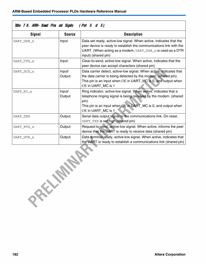
ARM-Based Embedded Processor PLDs Hardware Reference Manual
PRELIM
INARY IN
FORMAT
ION
UART_DSR_n Input Data set ready, active-low signal. When active, indicates that the peer device is ready to establish the communications link with the UART. (When acting as a modem, UART_DSR_n is used as a DTR input) (shared pin)
UART_CTS_n Input Clear-to-send, active-low signal. When active, indicates that the peer device can accept characters (shared pin)
UART_DCD_n Input/ Output
Data carrier detect, active-low signal. When active, indicates that the data carrier is being detected by the modem. (shared pin).This pin is an input when OE in UART_MC is 0, and output when OE in UART_MC is 1
UART_RI_n Input/ Output
Ring indicator, active-low signal. When active, indicates that a telephone ringing signal is being received by the modem. (shared pin).This pin is an input when OE in UART_MC is 0, and output when OE in UART_MC is 1
UART_TXD Output Serial data output signal to the communications link. On reset, UART_TXD is set high (shared pin)
UART_RTS_n Output Request-to-send, active-low signal. When active, informs the peer device that the UART is ready to receive data (shared pin)
UART_DTR_n Output Data terminal ready, active-low signal. When active, indicates that the UART is ready to establish a communications link (shared pin)
Table 78. ARM-Based Pins and Signals (Part 5 of 5)
Signal Source Description
182 Altera Corporation