Embed Size (px)
Citation preview
DOI: 10.1007/s00339-002-1444-2
Appl. Phys. A 76, 133–137 (2003)
Invi
ted
pape
rMaterials Science & ProcessingApplied Physics A
m. yousuf1,✉
s.b. qadri2
e.f. skelton1
Evidence for the existence of an unusualstructure in the nanorods of InSb1 The George Washington University, Washington, DC 20052, USA2 U.S. Naval Research Laboratory, Washington, DC 20375, USA
Received: 6 February 2002/Accepted: 26 March 2002Published online: 10 September 2002 • © Springer-Verlag 2002
ABSTRACT Motivated by the recent prediction that InSbnanometer-diameter filaments can exhibit exotic physical prop-erties, we have synthesized this material and have charac-terized the filaments. In this report, we describe the findingof an unusual phase of InSb. This new phase occurs whenan InSb filament has a diameter of less than 100 nm. High-resolution X-ray-diffraction studies of InSb filaments, havingradii ∼= 33.0 nm, indicate the InSb crystal lattice to be tetrag-onal, S.G. I4/mmm, with a unit-cell volume 12 times largerthan that of the β-tin phase observed in bulk InSb above2.0 GPa. The density of an InSb nanorod, as calculated fromX-ray-diffraction data, is ∼ 22% more than that of the zinc-blende phase of InSb at ambient conditions, implying that thenanorod experiences a pressure of ∼ 2 GPa. In contrast, InSbnanorods with radii ≥ 50.0 nm are observed to show zinc-blende structure and densities nearly the same as that of thebulk.
PACS 62.50.+p; 64.70.Nd; 71.20.Nr
Among AnB8−n semiconducting compounds, indium anti-monide is one of the most extensively studied materials [1–6]owing to its complex behavior under the application of pres-sure and temperature. The wide range of structural analogiesbetween the polymorphs of elemental and compound semi-conductors has been extended to InSb. The occurrence oftetragonal and orthorhombic phases at high pressure is wellestablished. We report here the first comprehensive crystalstructure analysis of InSb nanorods. Our results are consis-tent with the following previously noted observations: (i)nanophase materials are inherently under chemical pressure,(ii) mechanical and chemical pressures cause almost similarchanges in solids and (iii) there is a reasonable degree of sim-ilarity of pressure-induced behavior between elemental andcompound semiconductors.
We now recall briefly the role of pressure on phase stabil-ity in InSb, Si and Ge. Depending on the rate of pressurization,two pressure-induced structural sequences have been reported
✉ Fax: +1-202/767-5301; E-mail: [email protected]
in InSb. Under rapid application of pressure, the structural se-quence exhibited is [7–9]:
Cubic〈zinc-blende type(S.G.F43m)〉2.1 GPa−−−−→ Tetragonal〈β-tin type(S.G.I41/amd)〉
+orthorhombic I(S.G.Immm)
∆P−→ Orthorhombic I(Immm)
3 GPa−−−→ Orthorhombic II(super-Cmcm)
10 GPa−−−−→ P5(unknown structure)
∆P−→ OrthorhombicI(Immm)
17 GPa−−−−→ Intermediate phase(unknown structure)
∆P−→ Cubic(body-centered).
In contrast, under a slow rate of pressurization, with a longholding time for each applied pressure, a second structural se-quence has been observed. This sequence is similar to the oneindicated above except for the absence of the β-tin phase. Al-though the absence of the β-tin phase in the equilibrium (P, T )
diagram of InSb has been amply demonstrated, it is the ob-jective of the present report to show that the situation is fardifferent in relation to InSb of low dimensionality.
Complex behavior of InSb under pressure arises due to thesymmetry breaking in the tetrahedral covalent bonding net-work, and the consequent change in the nature of the chemicalbonding [10] giving rise to the observed sequence of structuraltransformations.
Jayaraman et al. detected a volume decrease of ∼ 20%near 2.0 GPa at room temperature. They suggested that thehigh-pressure phase was a diatomic analogue of the β-tinstructure [1]. Recently, Crain et al., based on Rietveld re-finement, found that InSb at 2.5 GPa existed as a mixtureof two phases (β-tin: 80%; Imm2 : 20%). They showed ev-idence for the creation of an inversion-domain boundaryat the phase transition [11]. On the other hand, Nelmes etal. [7] noted that, at ∼ 2.1 GPa, InSb had two concurrentphases corresponding to tetragonal (β-tin: S.G. I41/amd)and orthorhombic (S.G. Immm) structures. With a slight in-crease in pressure, an increase in the concentration of theorthorhombic phase was found to occur at the expense of
134 Applied Physics A – Materials Science & Processing
the β-tin phase. At 2.3 GPa, InSb became a three-phase mix-ture, namely (i) the β-tin, (ii) the orthorhombic (Immm) and(iii) yet another orthorhombic (super-Cmcm) structure, hav-ing the calculated unit-cell volume of the β-tin phase, ∼ 25%smaller than that of the parent zinc-blende phase. For thesake of convenience, throughout this report, different phasesof InSb are referenced to the space groups to which they areassociated.
Above 3 GPa, initially it was suggested that the Immmphase changes into the Pmm2 phase, with a unit cell con-taining two formula units [6, 7]. Later, the same phase wasidentified as a superlattice structure with Cmcm symmetryand having a unit cell 12 times larger than that of the Pmm2unit cell [5]. The calculated lattice parameters of the superlat-tice structure were calculated as a = 5.847 Å, b = 6.140 Å andc = 16.791 Å, with four (a) and eight (f) equivalent positionsoccupied.
In contrast to binary III–V and II–VI semiconductors,elemental semiconductors such as Si and Ge undergo a cubic(diamond)-to-tetragonal(β-tin-type) structural transition.However, InSb is the only compound semiconductor that isknown to undergo a transition to the diatomic equivalent of theβ-tin structure under the rapid application of pressure [5]. Inthe pressure and temperature ranges of up to 8 GPa and 873 K,bulk InSb exhibits three solid phases, namely zinc-blende,Pmm2 (later modified to super-Cmcm) and Immm structures;however, the β-tin structure has not been observed [6].
InSb is a prototype III–V semiconductor having an en-ergy band gap, Eg, of 0.165 eV at 300 K and 0.23 eV at 0 K.Generally, it is observed that the value of Eg of most ofthe semiconductors decreases with the decrease in the lat-tice parameters. It has also been observed that semiconduc-tors in the nanometer realm show reduced lattice parame-ters and exhibit interesting optical, electrical and chemicalproperties [12, 13]. Due to its very large exciton Bohr ra-dius ∼ 65.5 nm, InSb appears to be an ideal candidate forexhibiting the features of a quantum dot as a result of theconfinement of electron and hole wave functions [14]. In thisregard, the model calculations by Lee and Mendoza showthat, by treating the simultaneous participation of multiplebosonic modes, it is possible to predict superconductivityin slender electronic systems of finite cross sections basedon the pairing interaction mediated by the multiple modesof acoustic plasmons [15]. The modes consist of the quasi-one-dimensional plasmons and the so-called slender acousticplasmons. Their calculations predicted that sub-50.0-nm fila-ments of InSb would exhibit a normal conducting to a super-conducting transition with a significantly high transition tem-perature (TC ≥ 200 K).
Very fine filaments of InSb having radii in the range of∼= 30.0 nm were fabricated, using a modified Taylor wire pro-cess. The details of the synthesis are given elsewhere [16,17]. High-resolution X-ray-diffraction scans were obtainedwith a Rigaku powder diffractometer using Cu Kα radiationfrom a rotating anode X-ray generator operated at 50 kV and200 mA. Efforts to collect the diffraction data from a singlestrand of InSb were unsuccessful, due to the small amountof diffracting material and X-ray absorption by the glassenvelopes. Therefore, a sample consisting of 12 filaments,spread over a glass substrate, was mounted on a goniometer
head of the diffractometer. The scattering power of a crys-tal (S), a dimensionless quantity, is a measure of the abil-ity of a material to scatter X-rays. For crystal structure de-termination, typically S should be between 1016 and 1017,though measurements have been performed with S rangingfrom 1010 to 1014 [17–19]. In our experimental configuration,with ∼ 100 µm3 crystal volume, the value of S is ∼= 1015 [20].
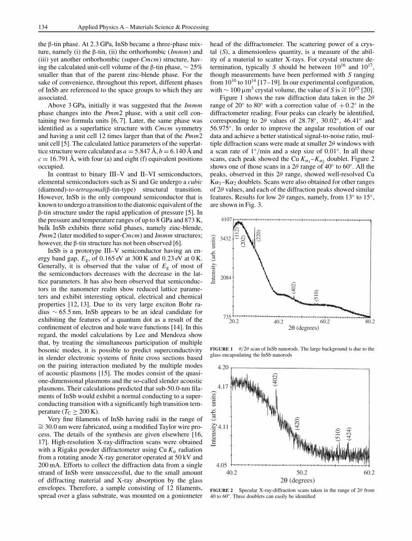
Figure 1 shows the raw diffraction data taken in the 2θ
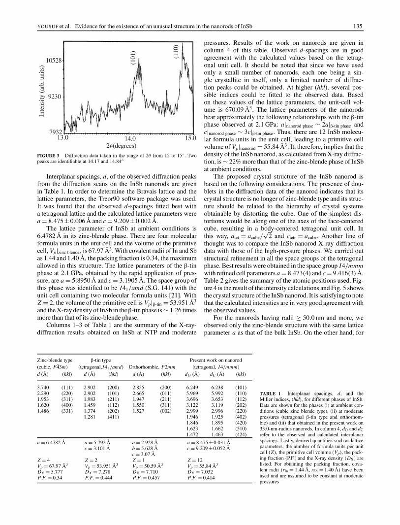
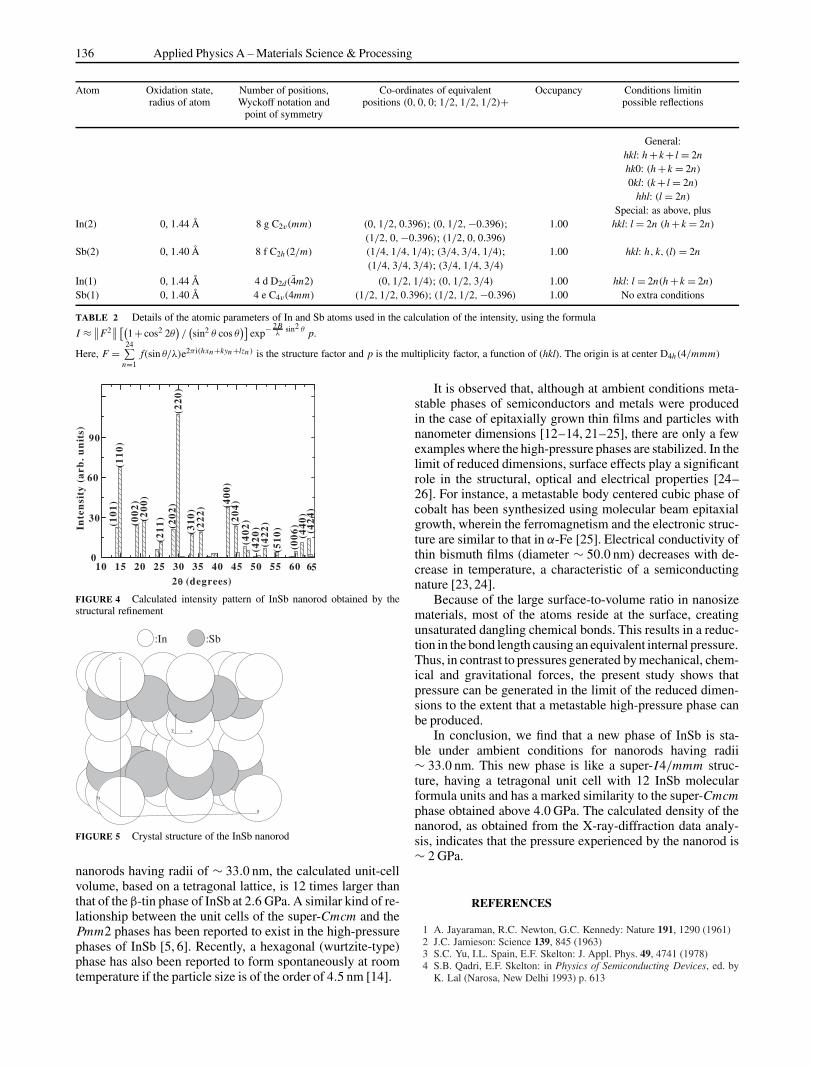
range of 20◦ to 80◦ with a correction value of +0.2◦ in thediffractometer reading. Four peaks can clearly be identified,corresponding to 2θ values of 28.78◦, 30.02◦, 46.41◦ and56.975◦. In order to improve the angular resolution of ourdata and achieve a better statistical signal-to-noise ratio, mul-tiple diffraction scans were made at smaller 2θ windows witha scan rate of 1◦/min and a step size of 0.01◦. In all thesescans, each peak showed the Cu Kα1–Kα2 doublet. Figure 2shows one of those scans in a 2θ range of 40◦ to 60◦. All thepeaks, observed in this 2θ range, showed well-resolved CuKα1–Kα2 doublets. Scans were also obtained for other rangesof 2θ values, and each of the diffraction peaks showed similarfeatures. Results for low 2θ ranges, namely, from 13◦ to 15◦,are shown in Fig. 3.
20.2 40.2 60.2 80.2735
2084
3432
4107
(112
)(2
02)
(220
)
(402
)
(510
)
2 (degrees)θ
Inte
nsity
(ar
b. u
nits
)
FIGURE 1 θ/2θ scan of InSb nanorods. The large background is due to theglass encapsulating the InSb nanorods
40.2 50.2 60.24.05
4.11
4.17
4.20
(402
)
(420
)
(510
)
(424
)
2 (degrees)θ
Inte
nsity
(ar
b. u
nits
)
FIGURE 2 Specular X-ray-diffraction scans taken in the range of 2θ from40 to 60◦. Three doublets can easily be identified
YOUSUF et al. Evidence for the existence of an unusual structure in the nanorods of InSb 135
13.0 14.0 15.0
(110
)
(101
)
10528
7932
9230
Inte
nsity
(ar
b. u
nits
)
2 (degrees)θ
FIGURE 3 Diffraction data taken in the range of 2θ from 12 to 15◦. Twopeaks are identifiable at 14.17 and 14.84◦
Interplanar spacings, d, of the observed diffraction peaksfrom the diffraction scans on the InSb nanorods are givenin Table 1. In order to determine the Bravais lattice and thelattice parameters, the Treor90 software package was used.It was found that the observed d-spacings fitted best witha tetragonal lattice and the calculated lattice parameters werea = 8.475±0.006 Å and c = 9.209±0.002 Å.
The lattice parameter of InSb at ambient conditions is6.4782 Å in its zinc-blende phase. There are four molecularformula units in the unit cell and the volume of the primitivecell, Vp|zinc blende, is 67.97 Å3. With covalent radii of In and Sbas 1.44 and 1.40 Å, the packing fraction is 0.34, the maximumallowed in this structure. The lattice parameters of the β-tinphase at 2.1 GPa, obtained by the rapid application of pres-sure, are a = 5.8950 Å and c = 3.1905 Å. The space group ofthis phase was identified to be I41/amd (S.G. 141) with theunit cell containing two molecular formula units [21]. WithZ = 2, the volume of the primitive cell is Vp|β-tin = 53.951 Å3
and the X-ray density of InSb in the β-tin phase is ∼ 1.26 timesmore than that of its zinc-blende phase.
Columns 1–3 of Table 1 are the summary of the X-ray-diffraction results obtained on InSb at NTP and moderate
Zinc-blende type β-tin type Present work on nanorod(cubic, F43m) (tetragonal,I41/amd) Orthorhombic, P2mm (tetragonal, I4/mmm)d (Å) (hkl) d (Å) (hkl) d (Å) (hkl) dO (Å) dC (Å) (hkl)
3.740 (111) 2.902 (200) 2.855 (200) 6.249 6.238 (101)2.290 (220) 2.902 (101) 2.665 (011) 5.969 5.992 (110)1.953 (311) 1.983 (211) 1.947 (211) 3.696 3.653 (112)1.620 (400) 1.459 (112) 1.550 (311) 3.122 3.119 (202)1.486 (331) 1.374 (202) 1.527 (002) 2.999 2.996 (220)
1.281 (411) 1.946 1.925 (402)1.846 1.895 (420)1.623 1.662 (510)1.472 1.463 (424)
a = 6.4782 Å a = 5.792 Å a = 2.928 Å a = 8.475±0.031 Åc = 3.101 Å b = 5.628 Å c = 9.209 ±0.052 Å
c = 3.07 ÅZ = 4 Z = 2 Z = 1 Z = 12Vp = 67.97 Å3 Vp = 53.951 Å3 Vp = 50.59 Å3 Vp = 55.84 Å3
DX = 5.777 DX = 7.278 DX = 7.710 DX = 7.032P.F. = 0.34 P.F. = 0.444 P.F. = 0.457 P.F. = 0.414
TABLE 1 Interplanar spacings, d, and theMiller indices, (hkl), for different phases of InSb.Data are shown for the phases (i) at ambient con-ditions (cubic zinc blende type), (ii) at moderatepressures (tetragonal β-tin type and orthorhom-bic) and (iii) that obtained in the present work on33.0-nm-radius nanorods. In column 4, dO and dCrefer to the observed and calculated interplanarspacings. Lastly, derived quantities such as latticeparameters, the number of formula units per unitcell (Z), the primitive cell volume (Vp), the pack-ing fraction (P.F.) and the X-ray density (DX) arelisted. For obtaining the packing fraction, cova-lent radii (rIn = 1.44 Å, rSb = 1.40 Å) have beenused and are assumed to be constant at moderatepressures
pressures. Results of the work on nanorods are given incolumn 4 of this table. Observed d-spacings are in goodagreement with the calculated values based on the tetrag-onal unit cell. It should be noted that since we have usedonly a small number of nanorods, each one being a sin-gle crystallite in itself, only a limited number of diffrac-tion peaks could be obtained. At higher (hkl), several pos-sible indices could be fitted to the observed data. Basedon these values of the lattice parameters, the unit-cell vol-ume is 670.09 Å3. The lattice parameters of the nanorodsbear approximately the following relationships with the β-tinphase observed at 2.1 GPa: a|nanorod phase ∼ 2a|β-tin phase andc|nanorod phase ∼ 3c|β-tin phase. Thus, there are 12 InSb molecu-lar formula units in the unit cell, leading to a primitive cellvolume of Vp|nanorod = 55.84 Å3. It, therefore, implies that thedensity of the InSb nanorod, as calculated from X-ray diffrac-tion, is ∼ 22% more than that of the zinc-blende phase of InSbat ambient conditions.
The proposed crystal structure of the InSb nanorod isbased on the following considerations. The presence of dou-blets in the diffraction data of the nanorod indicates that itscrystal structure is no longer of zinc-blende type and its struc-ture should be related to the hierarchy of crystal systemsobtainable by distorting the cube. One of the simplest dis-tortions would be along one of the axes of the face-centeredcube, resulting in a body-centered tetragonal unit cell. Inthis way, atet = acube/
√2 and ctetr = acube. Another line of
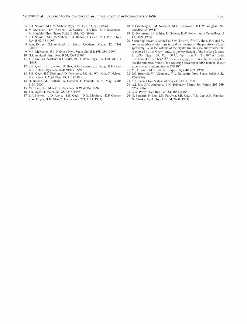
thought was to compare the InSb nanorod X-ray-diffractiondata with those of the high-pressure phases. We carried outstructural refinement in all the space groups of the tetragonalphase. Best results were obtained in the space group I4/mmmwith refined cell parameters a = 8.473(4) and c = 9.416(3) Å.Table 2 gives the summary of the atomic positions used. Fig-ure 4 is the result of the intensity calculations and Fig. 5 showsthe crystal structure of the InSb nanorod. It is satisfying to notethat the calculated intensities are in very good agreement withthe observed values.
For the nanorods having radii ≥ 50.0 nm and more, weobserved only the zinc-blende structure with the same latticeparameter a as that of the bulk InSb. On the other hand, for
136 Applied Physics A – Materials Science & Processing
Atom Oxidation state, Number of positions, Co-ordinates of equivalent Occupancy Conditions limitinradius of atom Wyckoff notation and positions (0, 0, 0; 1/2, 1/2, 1/2)+ possible reflections
point of symmetry
General:hkl: h + k + l = 2nhk0: (h + k = 2n)
0kl: (k + l = 2n)
hhl: (l = 2n)
Special: as above, plusIn(2) 0, 1.44 Å 8 g C2v(mm) (0, 1/2, 0.396); (0, 1/2,−0.396); 1.00 hkl: l = 2n (h + k = 2n)
(1/2, 0,−0.396); (1/2, 0, 0.396)
Sb(2) 0, 1.40 Å 8 f C2h(2/m) (1/4, 1/4, 1/4); (3/4, 3/4, 1/4); 1.00 hkl: h, k, (l) = 2n(1/4, 3/4, 3/4); (3/4, 1/4, 3/4)
In(1) 0, 1.44 Å 4 d D2d (4m2) (0, 1/2, 1/4); (0, 1/2, 3/4) 1.00 hkl: l = 2n(h + k = 2n)
Sb(1) 0, 1.40 Å 4 e C4v(4mm) (1/2, 1/2, 0.396); (1/2, 1/2, −0.396) 1.00 No extra conditions
TABLE 2 Details of the atomic parameters of In and Sb atoms used in the calculation of the intensity, using the formula
I ≈ ∥∥F2∥∥ [(
1+ cos2 2θ)/(sin2 θ cos θ
)]exp− 2B
λsin2 θ p.
Here, F =24∑
n=1f(sin θ/λ)e2πi(hxn+kyn+lzn ) is the structure factor and p is the multiplicity factor, a function of (hkl). The origin is at center D4h(4/mmm)
FIGURE 4 Calculated intensity pattern of InSb nanorod obtained by thestructural refinement
FIGURE 5 Crystal structure of the InSb nanorod
nanorods having radii of ∼ 33.0 nm, the calculated unit-cellvolume, based on a tetragonal lattice, is 12 times larger thanthat of the β-tin phase of InSb at 2.6 GPa. A similar kind of re-lationship between the unit cells of the super-Cmcm and thePmm2 phases has been reported to exist in the high-pressurephases of InSb [5, 6]. Recently, a hexagonal (wurtzite-type)phase has also been reported to form spontaneously at roomtemperature if the particle size is of the order of 4.5 nm [14].
It is observed that, although at ambient conditions meta-stable phases of semiconductors and metals were producedin the case of epitaxially grown thin films and particles withnanometer dimensions [12–14, 21–25], there are only a fewexamples where the high-pressure phases are stabilized. In thelimit of reduced dimensions, surface effects play a significantrole in the structural, optical and electrical properties [24–26]. For instance, a metastable body centered cubic phase ofcobalt has been synthesized using molecular beam epitaxialgrowth, wherein the ferromagnetism and the electronic struc-ture are similar to that in α-Fe [25]. Electrical conductivity ofthin bismuth films (diameter ∼ 50.0 nm) decreases with de-crease in temperature, a characteristic of a semiconductingnature [23, 24].
Because of the large surface-to-volume ratio in nanosizematerials, most of the atoms reside at the surface, creatingunsaturated dangling chemical bonds. This results in a reduc-tion in the bond length causing an equivalent internal pressure.Thus, in contrast to pressures generated by mechanical, chem-ical and gravitational forces, the present study shows thatpressure can be generated in the limit of the reduced dimen-sions to the extent that a metastable high-pressure phase canbe produced.
In conclusion, we find that a new phase of InSb is sta-ble under ambient conditions for nanorods having radii∼ 33.0 nm. This new phase is like a super-I4/mmm struc-ture, having a tetragonal unit cell with 12 InSb molecularformula units and has a marked similarity to the super-Cmcmphase obtained above 4.0 GPa. The calculated density of thenanorod, as obtained from the X-ray-diffraction data analy-sis, indicates that the pressure experienced by the nanorod is∼ 2 GPa.
REFERENCES
1 A. Jayaraman, R.C. Newton, G.C. Kennedy: Nature 191, 1290 (1961)2 J.C. Jamieson: Science 139, 845 (1963)3 S.C. Yu, I.L. Spain, E.F. Skelton: J. Appl. Phys. 49, 4741 (1978)4 S.B. Qadri, E.F. Skelton: in Physics of Semiconducting Devices, ed. by
K. Lal (Narosa, New Delhi 1993) p. 613
YOUSUF et al. Evidence for the existence of an unusual structure in the nanorods of InSb 137
5 R.J. Nelmes, M.I. McMahon: Phys. Rev. Lett. 77, 663 (1996)6 M. Mezouar, J.M. Besson, G. Syffose, J.P. Itie, D. Häusermann,
M. Hanfeld: Phys. Status Solidi B 198, 403 (1996)7 R.J. Nelmes, M.I. McMahon, P.D. Hatton, J. Crain, R.O. Pitz: Phys.
Rev. B 47, 35 (1993)8 A.A. Kelsey, G.J. Ackland: J. Phys.: Condens. Matter 12, 7161
(2000)9 M.I. McMahon, R.J. Nelmes: Phys. Status Solidi B 198, 389 (1996)
10 G.J. Ackland: Phys. Rev. B 50, 7389 (1994)11 J. Crain, G.J. Ackland, R.O. Piltz, P.D. Hatton: Phys. Rev. Lett. 70, 814
(1993)12 S.B. Qadri, E.F. Skelton, D. Hsu, A.D. Dinsmore, J. Yang, H.F. Gray,
B.R. Ratna: Phys. Rev. B 60, 9191 (1999)13 S.B. Qadri, E.F. Skelton, A.D. Dinsmore, J.Z. Hu, W.J. Kim, C. Nelson,
B.R. Ratna: J. Appl. Phys. 89, 115 (2001)14 D. Besson, M. Treilleux, A. Hoareau, C. Esnouf: Philos. Mag. A 80,
1139 (2000)15 Y.C. Lee, B.S. Mendoza: Phys. Rev. B 39, 4776 (1989)16 J.D. Ayers: J. Mater. Sci. 28, 2237 (1993)17 E.F. Skelton, J.D. Ayers, S.B. Qadri, N.E. Moulton, K.P. Cooper,
L.W. Finger, H.K. Mao, Z. Hu: Science 253, 1123 (1991)
18 P. Eisenberger, J.M. Newsam, M.E. Leonowicz, D.E.W. Vaughan: Na-ture 309, 45 (1984)
19 R. Bachmann, H. Kohler, H. Schulz, H.-P. Weber: Acta Crystallogr. A41, 1099 (1985)
20 Scattering power is defined as S = (F000/Vp)2VCλ3. Here, F000 and Vp
are the number of electrons in, and the volume of, the primitive cell, re-spectively. VC is the volume of the crystal (in this case, the volume thatis exposed by the X-rays) and λ is the wavelength of the incident X-rays.In InSb, F000 = 64, Vp = 50 Å3, VC = nπr2l = 2×10¹⁴ Å3 (withn = 12) and λ3 = 3.6565 Å3 (for λ = λKα1 |Cu = 1.5406 Å). This impliesthat the numerical value of the scattering power of an InSb filament in ourexperimental configuration is S ∼= 1015
21 M.D. Banus, M.C. Lavine: J. Appl. Phys. 40, 409 (1969)22 P.G. Borzyak, V.I. Vatamany, Y.A. Kulyupin: Phys. Status Solidi A 22,
K3 (1974)23 S.K. Saha: Phys. Status Solidi A 71, K173 (1982)24 A.I. Ilin, A.V. Andreeva, B.N. Tolkunov: Mater. Sci. Forum 207–209,
625 (1996)25 G.A. Prinz: Phys. Rev. Lett. 54, 1051 (1985)26 N. Samarth, H. Luo, J.K. Furdyna, S.B. Qadri, Y.R. Lee, A.K. Ramdas,
N. Otsuka: Appl. Phys. Lett. 54, 2680 (1989)