Embed Size (px)
Citation preview

2015 Microchip Technology Inc. DS50002333B
EVB-LAN9252-HBI
EtherCAT® Evaluation BoardUser’s Guide

DS50002333B-page 2 2015 Microchip Technology Inc.
Information contained in this publication regarding device applications and the like is provided only for your convenience and may besuperseded by updates. It is your responsibility to ensure that your application meets with your specifications. MICROCHIP MAKES NOREPRESENTATIONS OR WARRANTIES OF ANY KIND WHETHER EXPRESS OR IMPLIED, WRITTEN OR ORAL, STATUTORY OROTHERWISE, RELATED TO THE INFORMATION, INCLUDING BUT NOT LIMITED TO ITS CONDITION, QUALITY, PERFORMANCE,MERCHANTABILITY OR FITNESS FOR PURPOSE. Microchip disclaims all liability arising from this information and its use. Use of Micro-chip devices in life support and/or safety applications is entirely at the buyer’s risk, and the buyer agrees to defend, indemnify and holdharmless Microchip from any and all damages, claims, suits, or expenses resulting from such use. No licenses are conveyed, implicitly orotherwise, under any Microchip intellectual property rights.
Trademarks
The Microchip name and logo, the Microchip logo, dsPIC, FlashFlex, flexPWR, JukeBlox, KEELOQ, KEELOQ logo, Kleer, LANCheck, MediaLB, MOST, MOST logo, MPLAB, OptoLyzer, PIC, PICSTART, PIC32 logo, RightTouch, SpyNIC, SST, SST Logo, SuperFlash and UNI/O are registered trademarks of Microchip Technology Incorporated in the U.S.A. and other countries.
The Embedded Control Solutions Company and mTouch are registered trademarks of Microchip Technology Incorporated in the U.S.A.
Analog-for-the-Digital Age, BodyCom, chipKIT, chipKIT logo, CodeGuard, dsPICDEM, dsPICDEM.net, ECAN, In-Circuit Serial Programming, ICSP, Inter-Chip Connectivity, KleerNet, KleerNet logo, MiWi, MPASM, MPF, MPLAB Certified logo, MPLIB, MPLINK, MultiTRAK, NetDetach, Omniscient Code Generation, PICDEM, PICDEM.net, PICkit, PICtail, RightTouch logo, REAL ICE, SQI, Serial Quad I/O, Total Endurance, TSHARC, USBCheck, VariSense, ViewSpan, WiperLock, Wireless DNA, and ZENA are trademarks of Microchip Technology Incorporated in the U.S.A. and other countries.
SQTP is a service mark of Microchip Technology Incorporated in the U.S.A.
Silicon Storage Technology is a registered trademark of Microchip Technology Inc. in other countries.
GestIC is a registered trademarks of Microchip Technology Germany II GmbH & Co. KG, a subsidiary of Microchip Technology Inc., in other countries.
All other trademarks mentioned herein are property of their respective companies.
© 2015, Microchip Technology Incorporated, Printed in the U.S.A., All Rights Reserved.
EtherCAT® is registered trademark and patented technology, licensed by Beckhoff Automation GmbH, Germany.
ISBN: 9781632773722
Note the following details of the code protection feature on Microchip devices:
• Microchip products meet the specification contained in their particular Microchip Data Sheet.
• Microchip believes that its family of products is one of the most secure families of its kind on the market today, when used in the intended manner and under normal conditions.
• There are dishonest and possibly illegal methods used to breach the code protection feature. All of these methods, to our knowledge, require using the Microchip products in a manner outside the operating specifications contained in Microchip’s Data Sheets. Most likely, the person doing so is engaged in theft of intellectual property.
• Microchip is willing to work with the customer who is concerned about the integrity of their code.
• Neither Microchip nor any other semiconductor manufacturer can guarantee the security of their code. Code protection does not mean that we are guaranteeing the product as “unbreakable.”
Code protection is constantly evolving. We at Microchip are committed to continuously improving the code protection features of ourproducts. Attempts to break Microchip’s code protection feature may be a violation of the Digital Millennium Copyright Act. If such actsallow unauthorized access to your software or other copyrighted work, you may have a right to sue for relief under that Act.
Microchip received ISO/TS-16949:2009 certification for its worldwide headquarters, design and wafer fabrication facilities in Chandler and Tempe, Arizona; Gresham, Oregon and design centers in California and India. The Company’s quality system processes and procedures are for its PIC® MCUs and dsPIC® DSCs, KEELOQ® code hopping devices, Serial EEPROMs, microperipherals, nonvolatile memory and analog products. In addition, Microchip’s quality system for the design and manufacture of development systems is ISO 9001:2000 certified.
QUALITY MANAGEMENT SYSTEM CERTIFIED BY DNV
== ISO/TS 16949 ==

Object of Declaration: EVB-LAN9252-HBI
2015 Microchip Technology Inc. DS50002333B-page 3

EVB-LAN9252-HBI User’s Guide
NOTES:
DS50002333B-page 4 2015 Microchip Technology Inc.

EVB-LAN9252-HBIUSER’S GUIDE
Table of Contents
Preface ........................................................................................................................... 7Introduction............................................................................................................ 7
Document Layout .................................................................................................. 7
Conventions Used in this Guide ............................................................................ 8
The Microchip Web Site ........................................................................................ 9
Development Systems Customer Change Notification Service ............................ 9
Customer Support ................................................................................................. 9
Document Revision History ................................................................................. 10
Chapter 1. Overview1.1 Introduction ................................................................................................... 111.2 References ................................................................................................... 131.3 Terms and Abbreviations ............................................................................. 13
Chapter 2. Board Details & Configuration2.1 Power ........................................................................................................... 14
2.1.1 +5V Power ................................................................................................. 14
2.2 Resets .......................................................................................................... 142.2.1 Power-on Reset ......................................................................................... 142.2.2 Reset Out .................................................................................................. 142.2.3 GPIO Reset ............................................................................................... 14
2.3 Clock ............................................................................................................ 152.4 Configuration ................................................................................................ 15
2.4.1 Strap Options ............................................................................................ 162.4.2 LED Indicators ........................................................................................... 182.4.3 EEPROM Switch ....................................................................................... 192.4.4 DIGIO/HBI/SPI+GPIO Selection ................................................................ 192.4.5 SoC ........................................................................................................... 24
2.5 DIGIO & SPI+16GPIO Signals on P1 and P2 Headers ................................ 262.5.1 DIGIO on P1 and P2 Headers (up to 16 bits supported) ........................... 262.5.2 SPI+GPIO on P1 and P2 Headers (up to 16 bits supported) .................... 26
2.6 Limitations .................................................................................................... 272.7 Mechanicals ................................................................................................. 28
Chapter 3. Software Development Kit3.1 Prerequisites ................................................................................................ 29
3.1.1 Hardware Requirements ........................................................................... 293.1.2 Software Requirements ............................................................................. 29
3.2 ESC SDK Sample Overview ........................................................................ 293.2.1 User Module .............................................................................................. 303.2.2 EtherCAT Slave Stack ............................................................................... 30
2015 Microchip Technology Inc. DS50002333B-page 5

EVB-LAN9252-HBI User’s Guide
3.2.3 Hardware Abstraction Layer (HAL) ............................................................30
3.3 Using the Sample Project ............................................................................. 313.3.1 MPLAB IDE Project Settings & Firmware Download .................................313.3.2 Compiling and Programming SoC Firmware .............................................34
3.4 Programming the LAN9252 EEPROM ......................................................... 353.4.1 Programming LAN9252 EEPROM using the TwinCAT Master Tool .........35
Appendix A. Evaluation Board PhotoA.1 Introduction .................................................................................................. 38
Appendix B. Evaluation Board SchematicsB.1 Introduction .................................................................................................. 39
Appendix C. Bill of Materials (BOM)C.1 Introduction .................................................................................................. 48
Worldwide Sales and Service .....................................................................................52
DS50002333B-page 6 2015 Microchip Technology Inc.

EVB-LAN9252-HBIUSER’S GUIDE
Preface
INTRODUCTION
This chapter contains general information that will be useful to know before using the EVB-LAN9252-HBI. Items discussed in this chapter include:
• Document Layout
• Conventions Used in this Guide
• The Microchip Web Site
• Development Systems Customer Change Notification Service
• Customer Support
• Document Revision History
DOCUMENT LAYOUT
This document describes how to use the EVB-LAN9252-HBI as a development tool for the Microchip LAN9252 EtherCAT® slave controller. The manual layout is as follows:
• Chapter 1. “Overview” – Shows a brief description of the EVB-LAN9252-HBI.
• Chapter 2. “Board Details & Configuration” – Includes details and instructions for using the EVB-LAN9252-HBI.
• Chapter 3. “Software Development Kit” – Includes details and instructions for using the LAN9252 EtherCAT® slave stack firmware and SDK framework.
• Appendix A. “Evaluation Board Photo” – This appendix shows the EVB-LAN9252-HBI.
• Appendix B. “Evaluation Board Schematics” – This appendix shows the EVB-LAN9252-HBI schematics.
• Appendix C. “Bill of Materials (BOM)” – This appendix includes the EVB-LAN9252-HBI Bill of Materials (BOM).
NOTICE TO CUSTOMERS
All documentation becomes dated, and this manual is no exception. Microchip tools and documentation are constantly evolving to meet customer needs, so some actual dialogs and/or tool descriptions may differ from those in this document. Please refer to our web site (www.microchip.com) to obtain the latest documentation available.
Documents are identified with a “DS” number. This number is located on the bottom of each page, in front of the page number. The numbering convention for the DS number is “DSXXXXXA”, where “XXXXX” is the document number and “A” is the revision level of the document.
For the most up-to-date information on development tools, see the MPLAB® IDE online help. Select the Help menu, and then Topics to open a list of available online help files.
2015 Microchip Technology Inc. DS50002333B-page 7

EVB-LAN9252-HBI User’s Guide
CONVENTIONS USED IN THIS GUIDE
This manual uses the following documentation conventions:
DOCUMENTATION CONVENTIONS
Description Represents Examples
Arial font:
Italic characters Referenced books MPLAB® IDE User’s Guide
Emphasized text ...is the only compiler...
Initial caps A window the Output window
A dialog the Settings dialog
A menu selection select Enable Programmer
Quotes A field name in a window or dialog
“Save project before build”
Underlined, italic text with right angle bracket
A menu path File>Save
Bold characters A dialog button Click OK
A tab Click the Power tab
N‘Rnnnn A number in verilog format, where N is the total number of digits, R is the radix and n is a digit.
4‘b0010, 2‘hF1
Text in angle brackets < > A key on the keyboard Press <Enter>, <F1>
Courier New font:
Plain Courier New Sample source code #define START
Filenames autoexec.bat
File paths c:\mcc18\h
Keywords _asm, _endasm, static
Command-line options -Opa+, -Opa-
Bit values 0, 1
Constants 0xFF, ‘A’
Italic Courier New A variable argument file.o, where file can be any valid filename
Square brackets [ ] Optional arguments mcc18 [options] file [options]
Curly brackets and pipe character: { | }
Choice of mutually exclusive arguments; an OR selection
errorlevel {0|1}
Ellipses... Replaces repeated text var_name [, var_name...]
Represents code supplied by user
void main (void){ ...}
DS50002333B-page 8 2015 Microchip Technology Inc.

Preface
THE MICROCHIP WEB SITE
Microchip provides online support via our web site at www.microchip.com. This web site is used as a means to make files and information easily available to customers. Accessible by using your favorite Internet browser, the web site contains the following information:
• Product Support – Data sheets and errata, application notes and sample programs, design resources, user’s guides and hardware support documents, latest software releases and archived software
• General Technical Support – Frequently Asked Questions (FAQs), technical support requests, online discussion groups, Microchip consultant program member listing
• Business of Microchip – Product selector and ordering guides, latest Microchip press releases, listing of seminars and events, listings of Microchip sales offices, distributors and factory representatives
DEVELOPMENT SYSTEMS CUSTOMER CHANGE NOTIFICATION SERVICE
Microchip’s customer notification service helps keep customers current on Microchip products. Subscribers will receive e-mail notification whenever there are changes, updates, revisions or errata related to a specified product family or development tool of interest.
To register, access the Microchip web site at www.microchip.com, click on Customer Change Notification and follow the registration instructions.
The Development Systems product group categories are:• Compilers – The latest information on Microchip C compilers, assemblers, linkers
and other language tools. These include all MPLAB C compilers; all MPLAB assemblers (including MPASM assembler); all MPLAB linkers (including MPLINK object linker); and all MPLAB librarians (including MPLIB object librarian).
• Emulators – The latest information on Microchip in-circuit emulators.This includes the MPLAB REAL ICE and MPLAB ICE 2000 in-circuit emulators.
• In-Circuit Debuggers – The latest information on the Microchip in-circuit debuggers. This includes MPLAB ICD 3 in-circuit debuggers and PICkit 3 debug express.
• MPLAB IDE – The latest information on Microchip MPLAB IDE, the Windows Integrated Development Environment for development systems tools. This list is focused on the MPLAB IDE, MPLAB IDE Project Manager, MPLAB Editor and MPLAB SIM simulator, as well as general editing and debugging features.
• Programmers – The latest information on Microchip programmers. These include production programmers such as MPLAB REAL ICE in-circuit emulator, MPLAB ICD 3 in-circuit debugger and MPLAB PM3 device programmers. Also included are nonproduction development programmers such as PICSTART Plus and PIC-kit 2 and 3.
CUSTOMER SUPPORT
Users of Microchip products can receive assistance through several channels:
• Distributor or Representative
• Local Sales Office
• Field Application Engineer (FAE)
• Technical Support
2015 Microchip Technology Inc. DS50002333B-page 9

EVB-LAN9252-HBI User’s Guide
Customers should contact their distributor, representative or field application engineer (FAE) for support. Local sales offices are also available to help customers. A listing of sales offices and locations is included in the back of this document.
Technical support is available through the web site at: http://www.microchip.com/support
DOCUMENT REVISION HISTORY
Revision Section/Figure/Entry Correction
DS50002333B (05-12-15) All Updated board name to “EVB-LAN9252-HBI” throughout document, corrected misc. typos and grammatical errors.
Section 1.2 “References” Updated list of application notes
Section 2.4.4 “DIGIO/HBI/SPI+GPIO Selection”
Added additional information on DIGIO mode.
Table 2-13, Table 2-14, and Table 2-15
Simplified table and added note under each table for clarity.
DS50002333A (02-27-15) Initial Release of document
DS50002333B-page 10 2015 Microchip Technology Inc.

EVB-LAN9252-HBIUSER’S GUIDE
Chapter 1. Overview
1.1 INTRODUCTION
The LAN9252 is a 2-port EtherCAT® Slave Controller (ESC) with dual integrated Ether-net PHYs which each contain a full-duplex 100BASE-TX transceiver and support 100Mbps (100BASE-TX) operation. 100BASE-FX is supported via an external fiber transceiver.
Each port receives an EtherCAT® frame, performs frame checking and forwards it to the next port. Time stamps of received frames are generated when they are received. The Loop-back function of each port forwards the frames to the next logical port if there is either no link at a port, if the port is not available, or if the loop is closed for that port. The Loop-back function of port 0 forwards the frames to the EtherCAT® Processing Unit. The loop settings can be controlled by the EtherCAT® master.
Packets are forwarded in the following order:
Port 0 -> EtherCAT® Processing Unit -> Port 1 -> Port 2.
The EtherCAT® Processing Unit (EPU) receives, analyzes and processes the Ether-CAT® data stream. The main purpose of the EtherCAT® Processing unit is to enable and coordinate access to the internal registers and the memory space of the ESC, which can be addressed both from the EtherCAT® master and from the local applica-tion. Data exchange between master and slave applications is comparable to a dual-ported memory (process memory), enhanced by special functions for consistency checking (SyncManager) and data mapping (FMMU). Each FMMU performs bitwise mapping of logical EtherCAT® system addresses to physical device addresses.
The scope of this document is to describe the EVB-LAN9252-HBI setup, which sup-ports a HBI/SPI+GPIO Interface and corresponding jumper configurations. The LAN9252 is connected to an RJ45 Ethernet jack with integrated magnetics for 100BASE-TX connectivity. A simplified block diagram of the EVB-LAN9252-HBI is shown in Figure 1-1.
2015 Microchip Technology Inc. DS50002333B-page 11

EVB-LAN9252-HBI User’s Guide
FIGURE 1-1: EVB-LAN9252-HBI BLOCK DIAGRAM
MicrochipLAN9252
EEPROM
EVB-LAN9252-HBI
100BASE-TX Ethernet
Magnetics & RJ45
100BASE-TX Ethernet
Magnetics & RJ45
StrapsPort 0 Port 1
Crystal
Power Supply Module
Ethernet Ethernet
5V
07
815
07
815
Jum
per
Se
lect
ion
LEDs
LEDs
Switc
hes
Switc
hes
GP
IO C
ircu
it
HBI or SPI+GPIO Selection
HBI Mode Selection
Switc
hes
Eth
erC
AT
ID
Sel
ect
Board to Board Connector
Board to Board Connector
Onboard Soc PIC32MX795F512L
SPI/SQI/I2C AARDVARK
Fiber-SFP
Port 0
Fiber-SFP
Port 1
DS50002333B-page 12 2015 Microchip Technology Inc.

Overview
1.2 REFERENCES
Concepts and material available in the following documents may be helpful when read-ing this document. Visit www.microchip.com for the latest documentation.
• LAN9252 Data Sheet
• AN 8.13 Suggested Magnetics
• EVB-LAN9252-HBI Schematics
• The following application notes:
- AN1916 Integrating Microchip’s LAN9252 SDK with Beckhoff’s EtherCAT® SSC
- AN1920 Microchip LAN9252 EEPROM Configuration and Programming
- AN1907 Microchip LAN9252 Migration from Beckhoff ET1100
1.3 TERMS AND ABBREVIATIONS
IDE - Integrated Development Environment
ESC - EtherCAT® Slave Controller
EVB - Engineering Validation Board
HAL - Hardware Abstraction Layer
HBI - Host Bus Interface
SPI - Serial Protocol Interface
SSC - Slave Stack Code
2015 Microchip Technology Inc. DS50002333B-page 13

EVB-LAN9252-HBIUSER’S GUIDE
Chapter 2. Board Details & Configuration
This chapter includes sub-sections on the following EVB-LAN9252-HBI details:
• Power
• Resets
• Clock
• Configuration
• Limitations
• Mechanicals
2.1 POWER
2.1.1 +5V Power
Power is supplied to the LAN9252 by a +3.3V on-board regulator, which is powered by a +5V external wall adapter (Manufacturer: TRIAD MAGNETICS and P/N: WSU050-3000). The LAN9252 includes an internal +1.2V regulator which supplies power to the internal core logic. Assertion of the D1 Green LED indicates successful generation of +3.3V o/p. The SW1 switch must be in the ON position for the +5V to power the +3.3V regulator.
2.2 RESETS
2.2.1 Power-on Reset
A power-on reset occurs whenever power is initially applied to the LAN9252 or if the power is removed and reapplied to the LAN9252. This event resets all circuitry within the LAN9252. After initial power-on, the LAN9252 can be reset by pressing the reset switch SW2. The reset LED D2 will assert (red) when the LAN9252 is in reset condition. For stability, a delay of approximately 180ms is added from the +3.3V o/p to reset release.
2.2.2 Reset Out
The LAN9252 reset pin can be configured as an output to reset the SoC. The RST# pin becomes an open-drain output and is asserted for the minimum required time of 80ms.
2.2.3 GPIO Reset
The EVB-LAN9252-HBI provides the option to reset the LAN9252 through a PIC GPIO pin [95(RG14)]. The SW10 switch is used for this selection, as shown in Table 2-1.
TABLE 2-1: RESET CONFIGURATION SWITCH
Switch Short Pins Knob Position Function
SW10 1-3 1-2 System Reset (SYS_RESETN) (Default)
SW10 1-2 1-3 GPIO Reset (RST_GPIO)
2015 Microchip Technology Inc. DS50002333B-page 14

Board Details & Configuration
2.3 CLOCK
The EVB-LAN9252-HBI utilizes an external 25MHz 25ppm crystal from Cardinal Com-ponents Inc. (P/N: CSM1Z-A5B2C5-40-25.0D18-F).
2.4 CONFIGURATION
The following sub-sections describe the various board features and configuration set-tings. A top view of the EVB-LAN9252-HBI is shown in Figure 2-1.
FIGURE 2-1: EVB-LAN9252-HBI TOP VIEW WITH CALLOUTS
PIC32MX795F512L
5V
T
es
tpo
int
RJ45 (with Magnetics)
Port 1Port 0
Mic
roch
ip
LA
N92
52
Port 0LINK/ACT LED
Port 1LINK/ACT LED
Res
etS
trap
sE
EP
RO
MS
oC
E
EP
RO
MS
oC
S
ele
ctS
oC
R
es
etIC
SP
fo
r P
ICAdd On SoC EtherCAT Device ID Power Circuit
3.3
V
Tes
tpo
int
GP
IO
Cir
cu
itH
BI M
od
e
Sel
ect
HB
I/SP
I+G
PIO
S
ele
ctR
UN
LE
D
2015 Microchip Technology Inc. DS50002333B-page 15

EVB-LAN9252-HBI User’s Guide
2.4.1 Strap Options
2.4.1.1 CHIP MODE SELECTION
Table 2-2 details the LAN9252 chip mode configuration straps.
2.4.1.2 EEPROM SIZE CONFIGURATION
The EEPROM size configuration strap (J5 & J8) determines the supported EEPROM size range. A low selects 1Kbits (128 x 8) through 16Kbits (2K x 8)_24C16. A high selects 32Kbits (4K x 8) through 512Kbits (64K x 8) or 4Mbits (512K x 8)_24C512.
2.4.1.3 COPPER AND FIBER STRAPS
The LAN9252 supports 100BASE-TX (Copper) and 100BASE-FX (Fiber) modes. In 100BASE-FX operation, the presence of the receive signal is indicated by the external transceiver as either an open-drain, CMOS level, Loss of Signal (SFP) or a LVPECL Signal Detect (SFF).
This EVB supports 100BASE-TX (Copper) and SFP 100BASE-FX (Fiber) modes. By default Copper Mode is active. Fiber Mode is supported as an assembly option. To select the Copper or Fiber Mode, the respective strap and signal routing resister assembly options must to be configured.
TABLE 2-2: CHIP MODE CONFIGURATION STRAP
Header Description Pins Settings
J4,J6,J7,J9 Chip mode configuration strap inputs. This strap determines the number of active ports and port types.
1-2
2-3
Short 1-2 for high (pull-up) (Not supported in this EVB)Short 2-3 for low (pull-down) (default)
Note: This EVB supports Chip mode 00 which is 2-port mode, where Port 0 = PHY A and Port 1 = PHY B. This requires J4, J6, J7, and J9 to be pulled-down (2-3) shorted. All other configurations are not supported with this EVB.
TABLE 2-3: EEPROM SIZE CONFIGURATION STRAP
Header Description Pins Settings
J5, J8 EEPROM size configuration strap inputs. This strap deter-mines the supported EEPROM size range.
1-22-3
Short 1-2 for high (pull-up) (default)Short 2-3 for low (pull-down)
Note: Vendor part number for SFP: Finisar/FTLF1217P2
DS50002333B-page 16 2015 Microchip Technology Inc.

Board Details & Configuration
2.4.1.3.1 Copper Mode
The EVB-LAN9252-HBI is set to Copper Mode by default. Table 2-4 details the required strap resistor settings for Copper Mode operation.
Additionally, the signal routing resistors detailed in Table 2-5 must be assembled for Copper Mode operation.
2.4.1.3.2 Fiber Mode
The EVB-LAN9252-HBI support SFP type 100BASE-FX. To enable Fiber Mode, the respective strap and signal routing resistors must be configured.
Table 2-6 details the required strap resistor settings for Fiber Mode operation.
Additionally, the signal routing resistors detailed in Table 2-7 must be assembled for Fiber Mode operation.
TABLE 2-4: COPPER MODE STRAP RESISTORS
Resistors Description
R79 (10K) Configures Port 0 & 1 to Copper Mode
R76, R80 (10K) Configures Port 0 and Port 1 to Copper Mode, respectively
Note: R75, R77, and R78 must not be populated (DNP).
TABLE 2-5: COPPER MODE SIGNAL ROUTING RESISTORS
Resistors Description
R17, R19, R21, R23 Port 0 Copper Mode enabled
R31, R33, R35, R37 Port 1 Copper mode enabled
Note: R16, R18, R20, R22, R30, R32, R34, and R36 (0402 package) must not be populated (DNP).
Note: Copper Mode related resistors must be DNP while Fiber Mode is active (See Section 2.4.1.3.1 “Copper Mode”).
TABLE 2-6: FIBER MODE STRAP RESISTORS
Resistors Description
R77 (10K) Configures Port 0 & 1 to FX-LOS Mode
R75, R78 (10K) Configures Port 0 and Port 1 to Fiber Mode, respectively
Note: R76, R79, and R80 must not be populated (DNP).
TABLE 2-7: FIBER MODE SIGNAL ROUTING RESISTORS
Resistors Description
R16, R18, R20, R22 Port 0 Fiber Mode enabled
R30, R32, R34, R36 Port 1 Fiber mode enabled
Note: R17, R19, R21, R23, R31, R33, R35, and R37 (0402 package) must not be populated (DNP).
2015 Microchip Technology Inc. DS50002333B-page 17

EVB-LAN9252-HBI User’s Guide
2.4.1.3.3 FX-LOS Fiber Mode Strap
FX-LOS strap details are shown in Table 2-8. These strap settings determine if the ports are to operate in FX-LOS Fiber Mode or FX-SD/Copper Mode.
2.4.2 LED Indicators
The D3 and D4 LEDs are used to indicate the Link/Activity status on the corresponding EVB ports, as detailed in Table 2-9. The Link/Act LED should be ON at each port when the cable is present. If the Link/Act LED is not ON, it indicates there is an issue with the connection or cable.
Additionally, the D5 LED is used as a RUN indicator (green) to show the AL status of the EtherCAT® State Machine (ESM), as detailed in Table 2-10.
TABLE 2-8: FX-LOS MODE STRAP SETTINGS
R77 (10K) R79 (10K)Reference Voltage (V)
Function
Populate DNP 3.3 A level above 2V selects FX-LOS for Port 0 and Port 1
Populate Populate 1.5 A level greater than 1.5V and below 2V selects FX-LOS for Port 0 and FX-SD / copper twisted pair for Port 1, further determined by FXSDB
DNP Populate 0 (Default) A level of 0V selects FX-SD / copper twisted pair for Ports 0 and 1, further determined by FXSDA and FXSDB
Note: The above strap details describe the LAN9252 function. This EVB does not support SFF Fiber Mode. Therefore, FX-SD related straps are not applica-ble.
TABLE 2-9: D3 AND D4 LINK/ACTIVITY LED STATUS INDICATORS
State Description
Off Link is down
Flashing Green Link is up with activity
Steady Green Link is up with no activity
TABLE 2-10: D5 RUN LED STATUS INDICATOR
State Description
Off The device is in the INITIALIZATION state
Blinking (on 200ms, off 200ms) The device is in the PRE-OPERATIONAL state
Single Flash (on 200ms, off 1000ms) The device is in the SAFE-OPERATIONAL state
On The device is in the OPERATIONAL state
Flickering (on 50ms, off 50ms) The device is booting and has not yet entered the INITIALIZATION state, or the device is in the BOOTSTRAP state and firmware download is in progress. (Optional. Off when not implemented.)
DS50002333B-page 18 2015 Microchip Technology Inc.

Board Details & Configuration
2.4.3 EEPROM Switch
The EVB-LAN9252-HBI utilizes 0x50 (7-bit) I2C slave addressing. The SW3 switch can be used to select the A0, A1, and A2 address bits, as shown in Figure 2-2 and Table 2-11. The eighth bit of the slave address determines if the master device wants to read or write to the EEPROM (24FC512).
FIGURE 2-2: SLAVE ADDRESS ALLOCATION
2.4.4 DIGIO/HBI/SPI+GPIO Selection
The EVB-LAN9252-HBI supports three LAN9252 configurations:
• DIGIO Mode
• HBI Mode
• SPI + 16 GPIO Mode
DIGIO and HBI modes use the same switch configuration. The DIGIO/HBI or SPI+GPIO configuration is selected using the DPDT SW11 to SW21 switches. By default, the EVB is set to DIGIO mode and no code is programmed to the on-board PIC32MX. In DIGIO mode, headers P1 and P2 can be used to probe the input and out-put control signals. It is not possible to configure the input or see to output on the LED on the EVB. Refer to Table 2-22 for a mapping of the DIGIO signals on the P1 and P2 headers.
TABLE 2-11: EEPROM SWITCH
Switch Description Settings
SW3 I2C EEPROM address selection switch (A0, A1, A2). See Figure 2-2.
ON for logic 0 (default)OFF for logic 1
R/W AA1 A00 A20 11
Start Read/Write
Slave Address
Note: The PDI configuration which is selected in hardware must match with the PDI configuration that is chosen in the EtherCAT SDK during the SSC inte-gration process. An appropriate PDI configuration must be set in the ESC configuration area of the EEPROM.
2015 Microchip Technology Inc. DS50002333B-page 19

EVB-LAN9252-HBI User’s Guide
FIGURE 2-3: SW11-SW21 DIGIO/HBI/SPI+GPIO MODE SELECTION
2.4.4.1 HBI MODE SELECTION
The LAN9252 supports six HBI modes. These six HBI modes (Multiplexed Modes and Indexed Modes) can be selected using the SPST switches (P/N: 450301014042-Wurth Electronics) SW5 through SW9 and SW22 through SW25. Through the switches the LAN9252 HBI signals are connected to the SoC.
2.4.4.1.1 Multiplexed Modes
The following four HBI Multiplexed Modes are supported:
1. 8-bit Multiplexed single-phase mode
2. 16-bit Multiplexed single-phase mode
3. 8-bit Multiplexed dual-phase mode
4. 16-bit Multiplexed dual-phase mode
Each HBI Multiplexed Mode requires an updated ESI file, EEPROM and PDI driver with configured SSC to be programmed to the PIC32MX. For additional software informa-tion, refer to Chapter 3. “Software Development Kit”.
Figure 2-4 details the switch selection for Multiplexed Mode. All four Multiplexed Modes utilize the same switch positions.
FIGURE 2-4: MULTIPLEXED HBI MODE SELECTION
TABLE 2-12: HBI/SPI+GPIO SWITCH CONFIGURATIONS
Switch Description Settings
SW11 to SW21 Up DIGIO/HBI Mode (Default)
SW11 to SW21 Down SPI+GPIO Mode
DIGIO/HBI Mode
SPI+GPIO Mode
Note: For switch P/N: 450301014042, pin 1 is at the middle of the switch. To short 1-2, knob position must be in the 1-3 position, and vice versa.
DS50002333B-page 20 2015 Microchip Technology Inc.

Board Details & Configuration
Table 2-13 details the switch selection for Multiplexed Mode.
2.4.4.1.2 Indexed Mode
There are 2 different Indexed modes, 8-bit and 16-bit. Each HBI Indexed Mode requires an updated ESI file, EEPROM and PDI driver with configured SSC to be programmed to the PIC32MX. For additional software information, refer to Chapter 3. “Software Development Kit”.
8-Bit Indexed Mode
Figure 2-5 details the switch selection for 8-Bit Indexed Mode.
FIGURE 2-5: 8-BIT INDEXED HBI MODE SELECTION
TABLE 2-13: MULTIPLEXED HBI MODE SELECTION
Switch Switch Knob Position
SW5 Down
SW6 Up
SW7 Down
SW8 Down
SW9 Down
SW22 Up
SW23 Down
SW24 Up
SW25 Up
Note: When the switch knob is in the down position, pins 1-2 are shorted. When then switch known is in the up position, pins 1-3 are shorted.
2015 Microchip Technology Inc. DS50002333B-page 21

EVB-LAN9252-HBI User’s Guide
Table 2-14 details the switch selection for 8-bit Indexed HBI Mode.
16-Bit Indexed Mode
Figure 2-6 details the switch selection for 16-Bit Indexed Mode.
FIGURE 2-6: 16-BIT INDEXED HBI MODE SELECTION
Table 2-15 details the switch selection for 16-bit Indexed HBI Mode.
TABLE 2-14: 8-BIT INDEXED HBI MODE SELECTION
Switch Switch Knob Position
SW5 Up
SW6 Up
SW7 Up
SW8 Down
SW9 Up
SW22 Up
SW23 Down
SW24 Down
SW25 Down
Note: When the switch knob is in the down position, pins 1-2 are shorted. When then switch known is in the up position, pins 1-3 are shorted.
TABLE 2-15: 16-BIT INDEXED HBI MODE SELECTION
Switch Switch Knob Position
SW5 Down
SW6 Up
SW7 Up
SW8 Down
SW9 Up
SW22 Up
SW23 Down
SW24 X (Don’t Care)
SW25 Down
Note: When the switch knob is in the down position, pins 1-2 are shorted. When then switch known is in the up position, pins 1-3 are shorted.
Note: If any other SoC is used, the user must check what modes are supported and configure the HBI mode selection switches accordingly.
DS50002333B-page 22 2015 Microchip Technology Inc.
Board Details & Configuration
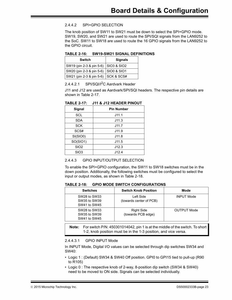
2.4.4.2 SPI+GPIO SELECTION
The knob position of SW11 to SW21 must be down to select the SPI+GPIO mode. SW19, SW20, and SW21 are used to route the SPI/SQI signals from the LAN9252 to the SoC. SW11 to SW18 are used to route the 16 GPIO signals from the LAN9252 to the GPIO circuit.
2.4.4.2.1 SPI/SQI/I2C Aardvark Header
J11 and J12 are used as Aardvark/SPI/SQI headers. The respective pin details are shown in Table 2-17.
2.4.4.3 GPIO INPUT/OUTPUT SELECTION
To enable the SPI+GPIO configuration, the SW11 to SW18 switches must be in the down position. Additionally, the following switches must be configured to select the input or output modes, as shown in Table 2-18.
2.4.4.3.1 GPIO INPUT Mode
In INPUT Mode, Digital I/O values can be selected through dip switches SW34 and SW40:
• Logic 1 : (Default) SW34 & SW40 Off position. GPI0 to GPI15 tied to pull-up (R90 to R105)
• Logic 0 : The respective knob of 2-way, 8-position dip switch (SW34 & SW40) need to be moved to ON side. Signals can be selected individually.
TABLE 2-16: SW19-SW21 SIGNAL DEFINITIONS
Switch Signals
SW19 (pin 2-3 & pin 5-6) SIO3 & SIO2
SW20 (pin 2-3 & pin 5-6) SIO0 & SIO1
SW21 (pin 2-3 & pin 5-6) SCK & SCS#
TABLE 2-17: J11 & J12 HEADER PINOUT
Signal Pin Number
SCL J11.1
SDA J11.3
SCK J11.7
SCS# J11.9
SI(SIO0) J11.8
SO(SIO1) J11.5
SIO2 J12.3
SIO3 J12.4
TABLE 2-18: GPIO MODE SWITCH CONFIGURATIONS
Switches Switch Knob Position Mode
SW28 to SW33SW35 to SW39SW41 to SW45
Left Side(towards center of PCB)
INPUT Mode
SW28 to SW33SW35 to SW39SW41 to SW45
Right Side(towards PCB edge)
OUTPUT Mode
Note: For switch P/N: 450301014042, pin 1 is at the middle of the switch. To short 1-2, knob position must be in the 1-3 position, and vice versa.
2015 Microchip Technology Inc. DS50002333B-page 23

EVB-LAN9252-HBI User’s Guide
2.4.4.3.2 GPIO OUTPUT Mode
In OUTPUT Mode, updated GPO values will be seen on the green LEDs (D7 to D22):
• Logic 1 : LED illuminated (green)
• Logic 0 : LED not illuminated.
2.4.5 SoC
The EVB-LAN9252-HBI supports both an on-board SoC and add-on SoC. By default, the on-board SoC is enabled. However, an external add-on SoC can be connected via the add-on SoC headers P1 and P2. The SoC selection is configured via the SW26 switch, as detailed in the following subsections.
2.4.5.1 SOC SELECTION
The SW26 switch selects the enabled SoC. The SW26 switch knob position must be down (Text = “PIC”) to select the on-board PIC. If the switch knob position is up (Text = “PIM”), then the add-on board/SoC is selected and the on-board PIC is always in the reset state. Whenever an add-on board/SoC is used, the switch knob must be in the up position.
2.4.5.2 ON-BOARD PIC
By default, the on-board Microchip PIC32MX795F512L (U7) is used as the default SoC. The LAN9252 can be connected to the PIC using either an HBI or SPI interface. The selection switches must be configured accordingly to enable the desired interface. Refer to Section 2.4.4 “DIGIO/HBI/SPI+GPIO Selection” and Section 2.4.4.1 “HBI Mode Selection” for additional details.
2.4.5.2.1 Reset
SW27 is used to reset the on-board PIC. The LAN9252 can also reset the SoC if the reset pin is configured to output mode. For stability, a delay of approximately 180ms is added from the 3.3V o/p to reset release.
2.4.5.2.2 ICSP Header
The on-board PIC programing is performed using the ICSP header J13. Table 2-20 details the ICSP header pinout
Note: The LED (D7 to D22) anode is connected to ASIC.
TABLE 2-19: SOC SELECTION
Switch Position Settings
SW26 Down On-board PIC enabled
SW26 Up Add-on board/SoC enabled
TABLE 2-20: J13 ICSP HEADER PINOUT
J13 Pin Settings
1 MLCR
2 3V3
3 GND
4 PGD2
5 PGC2
6 NC
DS50002333B-page 24 2015 Microchip Technology Inc.

Board Details & Configuration
2.4.5.2.3 SoC EEPROM
The EVB-LAN9252-HBI provides an optional SoC EEPROM. Some SoCs may require an EEPROM. However, the PIC on-board SoC and PIC based add-on SoC boards do not require this EEPROM.
2.4.5.3 ADD-ON SOC
An add-on board can be attached to the EVB-LAN9252-HBI to use an add-on SoC. The add-on board must be mounted to the P1 and P2 connectors (2x23, 100mil normal gold plated berg stick). The SW26 switch must be in the up position when using an add-on SoC. Additionally, the J10 2-pin jumper must be shorted to route power to the add-on board from the EVB-LAN9252-HBI.
2.4.5.4 ESC ID SELECT
The signals shown in Table 2-21 are provided as EtherCAT® ID selection for complex ESCs. Switches SW7, SW8 and respective pull-up resistors are used to configure the ID select signals high or low. By default, the EtherCAT® ID values is set to 5. To achieve this, ID0 and ID2 are high via pull-up resistors, while the remainder of the ID select sig-nals are low (ID1, ID3-ID15). When required, setting the respective switch knob to the on position will change the ID select signal to low.
TABLE 2-21: ID SELECT SIGNALS
ID Selection Signal Signal Name PIC Pin Number Switch Pin Number
ID0 ID0_SELECT_RB0 25 SW7.1
ID1 ID_SELECT_RB1 24 SW7.2
ID2 ID_SELECT_RB2 23 SW7.3
ID3 ID_SELECT_RB3 22 SW7.4
ID4 ID_SELECT_RB4 21 SW7.5
ID5 ID_SELECT_RB5 20 SW7.6
ID6 ID_SELECT_RB8 32 SW7.7
ID7 ID_SELECT_RB9 33 SW7.8
ID8 ID_SELECT_RB10 34 SW8.1
ID9 ID_SELECT_RB11 35 SW8.2
ID10 ID_SELECT_RB12 41 SW8.3
ID11 ID_SELECT_RB13 42 SW8.4
ID12 ID_SELECT_RC1 6 SW8.5
ID13 ID_SELECT_RC2 7 SW8.6
ID14 ID_SELECT_RC3 8 SW8.7
ID15 ID_SELECT_RC4 9 SW8.8
2015 Microchip Technology Inc. DS50002333B-page 25
EVB-LAN9252-HBI User’s Guide
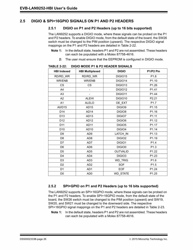
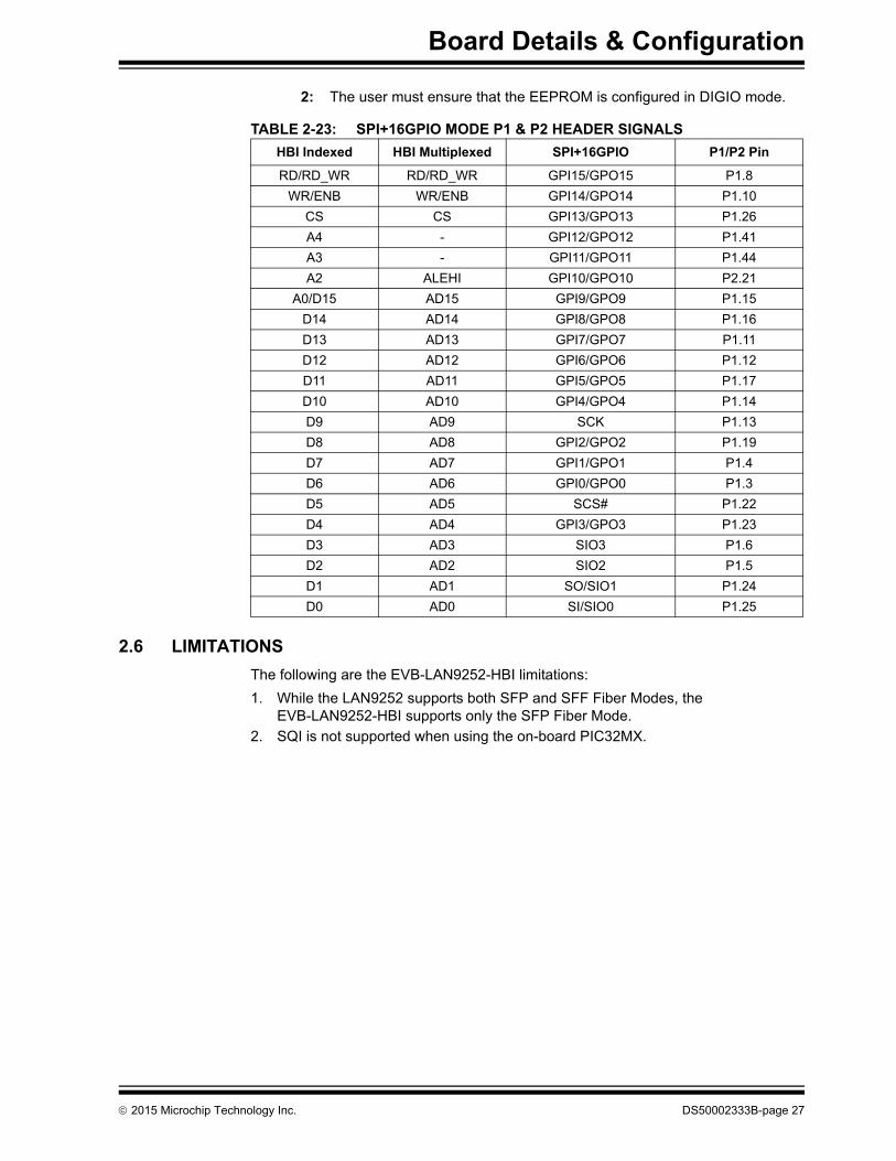
2.5 DIGIO & SPI+16GPIO SIGNALS ON P1 AND P2 HEADERS
2.5.1 DIGIO on P1 and P2 Headers (up to 16 bits supported)
The LAN9252 supports a DIGIO mode, where these signals can be probed on the P1 and P2 headers. To enable DIGIO mode, from the default state of the board, the SW26 switch must be changed to the PIM position (upward). The respective DIGIO signal mappings on the P1 and P2 headers are detailed in Table 2-22.
Note 1: In the default state, headers P1 and P2 are not assembled. These headers can each be populated with a Molex 87758-4616.
2: The user must ensure that the EEPROM is configured in DIGIO mode.
2.5.2 SPI+GPIO on P1 and P2 Headers (up to 16 bits supported)
The LAN9252 supports an SPI+16GPIO mode, where these signals can be probed on the P1 and P2 headers. To enable SPI+16GPIO mode, from the default state of the board, the SW26 switch must be changed to the PIM position (upward) and SW19, SW20, and SW21 must be changed to the downward side. The respective SPI+16GPIO signal mappings on the P1 and P2 headers are detailed in Table 2-23.
Note 1: In the default state, headers P1 and P2 are not assembled. These headers can each be populated with a Molex 87758-4616.
TABLE 2-22: DIGIO MODE P1 & P2 HEADER SIGNALS
HBI Indexed HBI Multiplexed DIGIO P1/P2 Pin
RD/RD_WR RD/RD_WR DIGIO15 P1.8
WR/ENB WR/ENB DIGIO14 P1.10
CS CS DIGIO13 P1.26
A4 - DIGIO12 P1.41
A3 - DIGIO11 P1.44
A2 ALEHI DIGIO10 P2.21
A1 ALELO OE_EXT P1.7
A0/D15 AD15 DIGIO9 P1.15
D14 AD14 DIGIO8 P1.16
D13 AD13 DIGIO7 P1.11
D12 AD12 DIGIO6 P1.12
D11 AD11 DIGIO5 P1.17
D10 AD10 DIGIO4 P1.14
D9 AD9 LATCH_IN P1.13
D8 AD8 DIGIO2 P1.19
D7 AD7 DIGIO1 P1.4
D6 AD6 DIGIO0 P1.3
D5 AD5 OUTVALID P1.22
D4 AD4 DIGIO3 P1.23
D3 AD3 WD_TRIG P1.6
D2 AD2 SOF P1.5
D1 AD1 EOF P1.24
D0 AD0 WD_STATE P1.25
DS50002333B-page 26 2015 Microchip Technology Inc.
Board Details & Configuration
2: The user must ensure that the EEPROM is configured in DIGIO mode.
2.6 LIMITATIONS
The following are the EVB-LAN9252-HBI limitations:
1. While the LAN9252 supports both SFP and SFF Fiber Modes, the EVB-LAN9252-HBI supports only the SFP Fiber Mode.
2. SQI is not supported when using the on-board PIC32MX.
TABLE 2-23: SPI+16GPIO MODE P1 & P2 HEADER SIGNALS
HBI Indexed HBI Multiplexed SPI+16GPIO P1/P2 Pin
RD/RD_WR RD/RD_WR GPI15/GPO15 P1.8
WR/ENB WR/ENB GPI14/GPO14 P1.10
CS CS GPI13/GPO13 P1.26
A4 - GPI12/GPO12 P1.41
A3 - GPI11/GPO11 P1.44
A2 ALEHI GPI10/GPO10 P2.21
A0/D15 AD15 GPI9/GPO9 P1.15
D14 AD14 GPI8/GPO8 P1.16
D13 AD13 GPI7/GPO7 P1.11
D12 AD12 GPI6/GPO6 P1.12
D11 AD11 GPI5/GPO5 P1.17
D10 AD10 GPI4/GPO4 P1.14
D9 AD9 SCK P1.13
D8 AD8 GPI2/GPO2 P1.19
D7 AD7 GPI1/GPO1 P1.4
D6 AD6 GPI0/GPO0 P1.3
D5 AD5 SCS# P1.22
D4 AD4 GPI3/GPO3 P1.23
D3 AD3 SIO3 P1.6
D2 AD2 SIO2 P1.5
D1 AD1 SO/SIO1 P1.24
D0 AD0 SI/SIO0 P1.25
2015 Microchip Technology Inc. DS50002333B-page 27

EVB-LAN9252-HBI User’s Guide
2.7 MECHANICALS
FIGURE 2-7: EVB-LAN9252-HBI MECHANICAL DIMENSIONS
DS50002333B-page 28 2015 Microchip Technology Inc.
EVB-LAN9252-HBIUSER’S GUIDE
Chapter 3. Software Development Kit
This chapter explains the architecture of the LAN9252 EtherCAT® slave stack firmware sample and introduces the SDK framework for use with PIC32MX microcontroller for EVB-LAN9252-HBI development.
This chapter includes the following sub-sections:
• Prerequisites
• ESC SDK Sample Overview
• Using the Sample Project
• Programming the LAN9252 EEPROM
3.1 PREREQUISITES
3.1.1 Hardware Requirements
• EVB-LAN9252-HBI-SPI-SQI-GPIO
• Windows Host Machine with minimum 2GB RAM
• Programmers – Aardvark I2C/SPI Host Adapter, Pickit3 Programmer
3.1.2 Software Requirements
• MPLAB IDE v2.20 or higher
• MPLAB XC Compiler v1.33 or higher
• Total Phase Flash Centre V1.31 or higher
3.2 ESC SDK SAMPLE OVERVIEW
The LAN9252 ESC supports interfacing to an external SoC using an SPI or HBI inter-face. This PIC32 based SDK sample contains separate projects for HBI and SPI inter-faces.
This software SDK is developed as a bare-metal firmware implementation (not specific to any OS) designed to access the LAN9252 ESC features via an HBI or SPI interface. The EtherCAT® slave stack portion of the source is obtained from EtherCAT Technol-ogy Group.
This software project has been tested with the EVB-LAN9252-HBI using the PIC32MX SoC.
Figure 3-1 provides an architectural block diagram of the SDK’s various source mod-ules. The subsequent sections detail these blocks.
2015 Microchip Technology Inc. DS50002333B-page 29

EVB-LAN9252-HBI User’s Guide
FIGURE 3-1: PIC32 SOC FIRMWARE FRAMEWORK
3.2.1 User Module
3.2.1.1 SOC INITIALIZATION
This code block is part of the user application that boots the PIC microcontroller with the desired RAM configuration, clock speed, clock source and other related features of the controller, per the user’s configuration.
3.2.1.2 PERIPHERAL INITIALIZATION
This code block configures and initiates the core peripherals (UART, I2C, SPI) and external peripherals (EEPROM, LAN9252).
3.2.1.3 MAIN APPLICATION
This code block contains the code that runs the LAN9252 EtherCAT® slave module demo application.
3.2.2 EtherCAT Slave Stack
This code block contains the EtherCAT slave stack.
3.2.3 Hardware Abstraction Layer (HAL)
This code block contains the low level layer that provides software hooks/APIs to the application module and slave stack, allowing communication between these modules and the hardware resources. For additional information, refer to the ReadMe.txt file located in the project source folder.
DS50002333B-page 30 2015 Microchip Technology Inc.

Software Development Kit
3.3 USING THE SAMPLE PROJECT
3.3.1 MPLAB IDE Project Settings & Firmware Download
1. Once the EtherCAT SSC is integrated with LAN9252 SDK as detailed in “Integrat-ing LAN9252 - PIC32MX SDK with EtherCAT SSC from ETG” application note, Copy it to the desired directory. (For the purposes of this document, the Desk-top will be the target folder).
2. Open the MPLAB IDE and import the SSC project into the IDE.
FIGURE 3-2: MPLAB IDE OPEN PROJECT
2015 Microchip Technology Inc. DS50002333B-page 31

EVB-LAN9252-HBI User’s Guide
FIGURE 3-3: MPLAB IDE PROJECT DIRECTORY
The target directory contains two project folders:
• PIC32 Project Folder
• PIC32-SPI Project Folder
3.3.1.1 PIC32 PROJECT FOLDER
The PIC32 project folder contains the sample code that enables the LAN9252's HBI interface to communicate with the SoC. HBI demo code is provided for each of the LAN9252’s six HBI configurations. These configurations can be selected respectively from the configuration drop down box as shown in Figure 3-4.
TABLE 3-1: HBI CONFIGURATIONS
HBI Configuration (Project) Description
HBI_INDEXED_8BIT_XC32_PIC32MX79F512 8-bit Indexed mode
HBI_INDEXED_16BIT_XC32_PIC32MX79F512 16-bit Indexed mode
HBI_MSP_16BIT_XC32_PIC32MX79F512 16-bit Multiplexed single phase mode
HBI_MDP_8BIT_XC32_PIC32MX79F512 8-bit Multiplexed dual phase mode
HBI_MDP_16BIT_XC32_PIC32MX79F512 16-bit Multiplexed dual phase mode
DS50002333B-page 32 2015 Microchip Technology Inc.

Software Development Kit
FIGURE 3-4: MPLAB IDE HBI CONFIGURATION SELECTION
3.3.1.2 PIC32-SPI PROJECT FOLDER
The PIC32-SPI project folder contains the demo code that enables the LAN9252's SPI interface to communicate with the SoC.
• Refer to the LAN9252 data sheet for more details on these HBI interface and its modes.
• Refer to Section 2.4.4 “DIGIO/HBI/SPI+GPIO Selection” for SPI jumper configura-tions.
2015 Microchip Technology Inc. DS50002333B-page 33
EVB-LAN9252-HBI User’s Guide
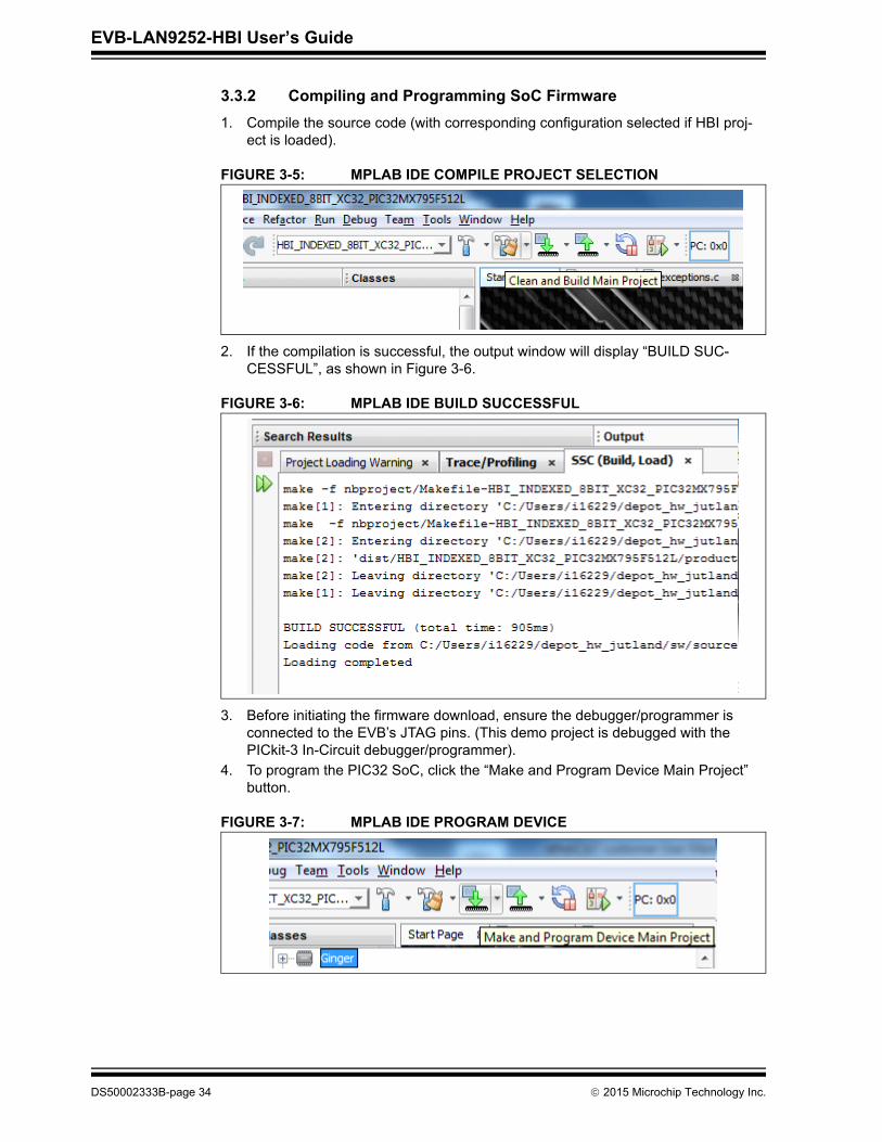
3.3.2 Compiling and Programming SoC Firmware
1. Compile the source code (with corresponding configuration selected if HBI proj-ect is loaded).
FIGURE 3-5: MPLAB IDE COMPILE PROJECT SELECTION
2. If the compilation is successful, the output window will display “BUILD SUC-CESSFUL”, as shown in Figure 3-6.
FIGURE 3-6: MPLAB IDE BUILD SUCCESSFUL
3. Before initiating the firmware download, ensure the debugger/programmer is connected to the EVB’s JTAG pins. (This demo project is debugged with the PICkit-3 In-Circuit debugger/programmer).
4. To program the PIC32 SoC, click the “Make and Program Device Main Project” button.
FIGURE 3-7: MPLAB IDE PROGRAM DEVICE
DS50002333B-page 34 2015 Microchip Technology Inc.

Software Development Kit
5. To debug the PIC32 SoC, click “Debug Main Project” button.
FIGURE 3-8: MPLAB IDE DEBUG DEVICE
3.4 PROGRAMMING THE LAN9252 EEPROM
The LAN9252 configures itself to the desired mode (SPI, 6 HBI modes) by reading the strap settings located in EEPROM. The LAN9252 EEPROM is programmed and vali-dated via the TwinCAT master tool. The EEPROM can also be programmed using an external IIC Master, like AARDVARK.
3.4.1 Programming LAN9252 EEPROM using the TwinCAT Master Tool
The programming procedure using the TwinCAT master tool is as follows:
Note 1: This example utilizes the TwinCAT tool. Procedures may differ when using other EtherCAT® master tools.
2: Ensure the system network properties are configured properly for the Eth-erCAT® frames, Ethernet cable linking your system, and EtherCAT® slave board.
1. Load the corresponding ESI file in the directory path "C:\TwinCAT\Io\EtherCAT". For this demo, the ESI file for the 16-Bit Multiplexed Single-Phase Mode is used.
2. If TwinCAT installed successfully, a TwinCAT icon will be shown in the bot-tom-right corner of the desktop. After clicking the icon, a pop-up list will display. Select “System Manager”, as shown in Figure 3-9.
FIGURE 3-9: TWINCAT SYSTEM MANAGER
2015 Microchip Technology Inc. DS50002333B-page 35

EVB-LAN9252-HBI User’s Guide
3. If any devices are present, delete them accordingly by clicking the device and selecting “Delete Device”, as shown in Figure 3-10.
FIGURE 3-10: TWINCAT DELETE DEVICE
4. Scan for EtherCAT® slave devices by clicking “I/O devices” and selecting “Scan Devices”, as shown in Figure 3-11.
FIGURE 3-11: TWINCAT SCAN DEVICES
DS50002333B-page 36 2015 Microchip Technology Inc.
Software Development Kit
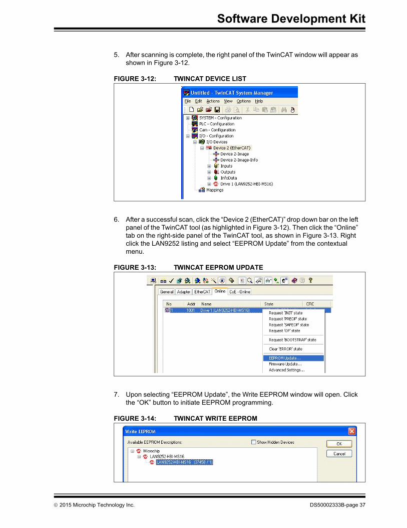
5. After scanning is complete, the right panel of the TwinCAT window will appear as shown in Figure 3-12.
FIGURE 3-12: TWINCAT DEVICE LIST
6. After a successful scan, click the “Device 2 (EtherCAT)” drop down bar on the left panel of the TwinCAT tool (as highlighted in Figure 3-12). Then click the “Online” tab on the right-side panel of the TwinCAT tool, as shown in Figure 3-13. Right click the LAN9252 listing and select “EEPROM Update” from the contextual menu.
FIGURE 3-13: TWINCAT EEPROM UPDATE
7. Upon selecting “EEPROM Update”, the Write EEPROM window will open. Click the “OK” button to initiate EEPROM programming.
FIGURE 3-14: TWINCAT WRITE EEPROM
2015 Microchip Technology Inc. DS50002333B-page 37

EVB-LAN9252-HBIUSER’S GUIDE
Appendix A. Evaluation Board Photo
A.1 INTRODUCTION
This appendix shows the EVB-LAN9252-HBI Evaluation Board.
FIGURE A-1: EVB-LAN9252-HBI EVALUATION BOARD
2015 Microchip Technology Inc. DS50002333B-page 38

EVB-LAN9252-HBIUSER’S GUIDE
Appendix B. Evaluation Board Schematics
B.1 INTRODUCTION
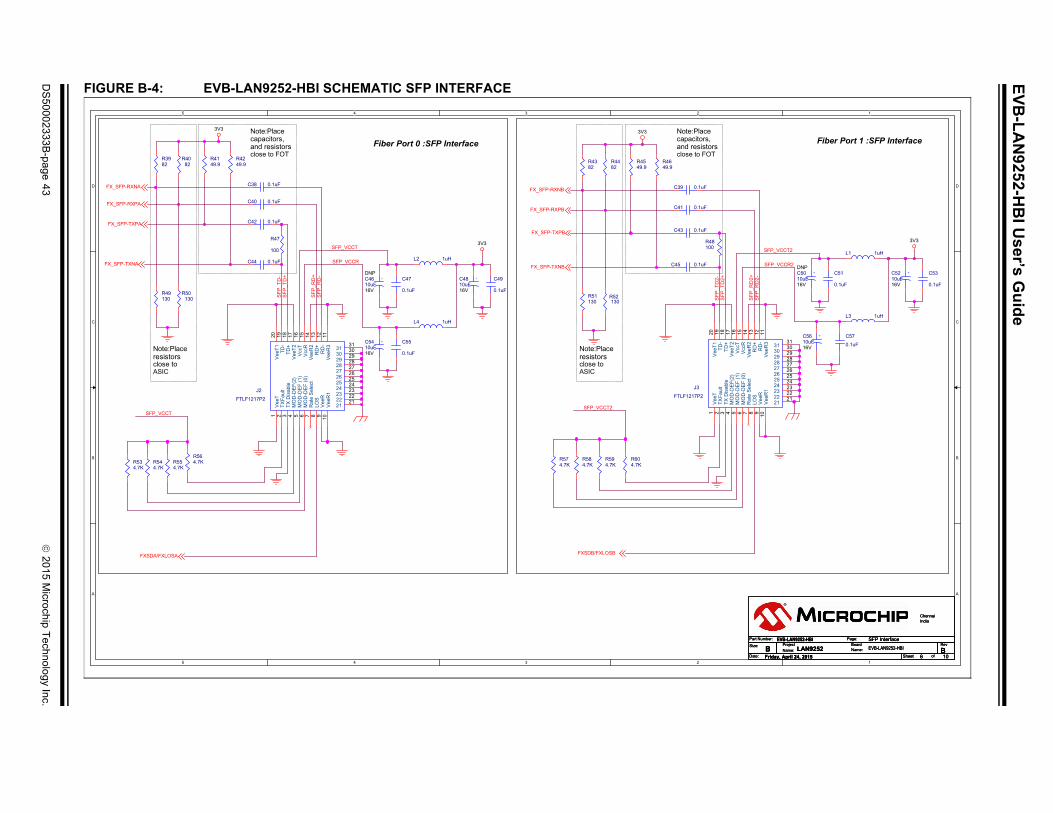
This appendix shows the EVB-LAN9252-HBI Evaluation Board Schematics.
2015 Microchip Technology Inc. DS50002333B-page 39

Evalu
ation
Bo
ard S
chem
atics
2015 Microchip T
echnology Inc.
DS
50002333B
-page 40
FIG
1
1
D D
C C
B B
A A
"3V3
Pre
sent
"
Only Ethercat sku
"Reset"
3V3
Size:
Part Number:Rev
Date: Sheet of
Chennai India
ProjectName:
Page:
Name:Board
�����������
BB3 10Friday, April 24, 2015
LAN9252Power Supply & RST
����������� Size:
Part Number:Rev
Date: Sheet of
Chennai India
ProjectName:
Page:
Name:Board
�����������
BB3 10Friday, April 24, 2015
LAN9252Power Supply & RST
����������� Size:
Part Number:Rev
Date: Sheet of
Chennai India
ProjectName:
Page:
Name:Board
�����������
BB3 10Friday, April 24, 2015
LAN9252Power Supply & RST
�����������
D1GRN
1A
2C
D2
Br_Red-RA
1A
2C
R2
1K
URE B-1: EVB-LAN9252-HBI SCHEMATIC POWER SUPPLY & RESET
5
5
4
4
3
3
2
2
Reset Generator
POWER SUPPLY
(Rb)(Ra)OKR-T/3-W12-C
3 V REGULATOR, 3A( 3V3 fixed when Rb=470E)
Note: 1.POR -> Reset to ASIC & SOC (Default)2.RESET O/P from ASIC -> Reset to EX-PHY (PORT2) & SOC :3.RESET from SOC (GPIO/RST-O/P) -> Reset to ASIC 4.RESET from Push Botton -> Reset to ASIC & SOC
RESET Options
5V_SWEN12_1
5V_EXT3V35V
3V3
3V3
3V3
3V3
RST#
TP1RED TP2
ORANGE
C3
0.1uF
C6
0.1uF
R8 1K
U1
3_Amp GND3
VIN2
ENABLE1
TRIM5VOUT4
R7100
1/10W1%
1 2
TP3BLACK
R54.75K1%
Q1NDS355AN_NMOS
1G 3
S
2 D
U2
TPS3125SOT23_5Threshold = 2.64VDelay = 180ms
RESET#1
GN
D2
RESET3
MR#4
VDD
5
SW1
P/N:1101M2S3CQE2Switch, SPDT, Slide
23
1
C4
10uF
C210uF25V
R610.0K1/10W1%
12
C5
0.1uF
U3
74LVC1G14
2 4
531
SW2
sw_pb_2P
R4470E1%
TP4BLACK
R33.30K1%
C1
4.7uF
DNP
R1 0E
R9 2.2K
R4A33E1%
FB1
2A/0.05DCR
J1
1
2
3

EV
B-L
AN
9252-HB
I User’s G
uid
e
DS
50002333B
-page 41
2015 M
icrochip Technolo
gy Inc.
1
1
D
C
B
A
Power Supply Filtering
Low
ESR
3V3VDDCR
Size:
Part Number:Rev
Date: Sheet of
Chennai India
ProjectName:
Page:
Name:Board
�����������
BB4 10Friday, April 24, 2015
LAN9252LAN9252
����������� Size:
Part Number:Rev
Date: Sheet of
Chennai India
ProjectName:
Page:
Name:Board
�����������
BB4 10Friday, April 24, 2015
LAN9252LAN9252
����������� Size:
Part Number:Rev
Date: Sheet of
Chennai India
ProjectName:
Page:
Name:Board
�����������
BB4 10Friday, April 24, 2015
LAN9252LAN9252
�����������
C14
0.1u
F
C17
0.1u
F
C11
0.1u
F
C21
0.1u
F
C22
0.1u
F
C15
0.1u
F
C13
0.1u
F
C20
470p
F
C12
1.0u
FD
NP
C16
0.1u
F
C10
0.1u
F
C19
1uF
C18
0.1u
F
FIGURE B-2: EVB-LAN9252-HBI SCHEMATIC LAN9252
5
5
4
4
3
3
2
2
D
C
B
A
Note: OSCVSS need to connect to Chip gnd.
REG_EN
RBIAS
VD
D12
TX1
VD
D12
TX2
VDD12TX2VDD12TX1
OSCOOSCI
3V3
VD
D33
TXR
X1
VD
D33
TXR
X2
VDDCR
VDD33TXRX1
VDD33TXRX2
3V3
3V3
3V3 3V3
FXSDA/FXLOSA
IRQ
ATEST/FXLOSEN
RXPARXNA
TXNATXPA
TXNBTXPBRXNBRXPB
FXSDB/FXLOSB
GPIO0GPIO1GPIO2
I2C2_SCLI2C2_SDA
RST#
FB3 2A/0.05DCR
R10 12.1K1%
C27 18pF
POWER
INT PORT0
INT PORT1
OSC
I2C
OTHER
SIGNALS
GPIO
(Only for
Lan9252)
U4A
LAN9252
FXSDENA/FXSDA/FXLOSA9
FXSDENB/FXSDB/FXLOSB10
VDD
33TX
RX1
51
TXNA52
TXPA53
RXNA54
RXPA55
VD
D12
TX1
56
RBIAS57
VD
D33
BIA
S58
VD
D12
TX2
59
RXPB60RXNB61TXPB62TXNB63
VDD
33TX
RX2
64
OSCI1
OSCO2
OSCVDD123
OSCVSS4
REG_EN7
ATEST/FXLOSEN8
RST#11
IRQ44
TESTMODE41
I2CSCL/EESCL/TCK43
I2CSDA/EESDA/TMS42
LINKACTLED0/TDO/LEDPOL0/CHIP_MODE048
LINKACTLED1/TDI/LEDPOL1/CHIP_MODE146
RUNLED/LEDPOL2/E2PSIZE45
VDD
335
VDD
IO1
14
VDD
IO2
20
VDD
IO3
32
VDD
IO4
37
VDD
IO5
47
VDD
CR
16
VDD
CR
224
VDD
CR
338
GN
D65
C25
0.1u
F
FB2 2A/0.05DCR
FB52A/0.05DCRBLM18EG221SN1D
C24
0.1uFC23
1.0uF
DNP
C8
0.1uF
C26 18pF
C9
1.0u
FD
NPC7
1.0uF
DNP
Y1 25.000MHz25ppm
12
FB4 2A/0.05DCR
BLM18EG221SN1D

Evalu
ation
Bo
ard S
chem
atics
2015 Microchip T
echnology Inc.
DS
50002333B
-page 42
FIG
1
1
D D
C C
B B
A A
Size:
Part Number:Rev
Date: Sheet of
Chennai India
ProjectName:
Page:
Name:Board
�����������
BB5 10Friday, April 24, 2015
LAN9252Copper Mode Interface
����������� Size:
Part Number:Rev
Date: Sheet of
Chennai India
ProjectName:
Page:
Name:Board
�����������
BB5 10Friday, April 24, 2015
LAN9252Copper Mode Interface
����������� Size:
Part Number:Rev
Date: Sheet of
Chennai India
ProjectName:
Page:
Name:Board
�����������
BB5 10Friday, April 24, 2015
LAN9252Copper Mode Interface
�����������
URE B-3: EVB-LAN9252-HBI SCHEMATIC COPPER MODE INTERFACE
5
5
4
4
3
3
2
2
Note:Capacitors C28 through C31 are optional for EMI purposesand are not populated on the LAN9252 evaluation board.These capacitors are required for operation in an EMIconstrained environment.
Note:Capacitors C33 through C36 are optional for EMI purposesand are not populated on the LAN9252 evaluation board.These capacitors are required for operation in an EMIconstrained environment.
Port 0
Port 1
COP-RXPA
COP-TXNA
COP-RXNA
COP-TXPA
COP-RXPB
COP-TXNB
COP-RXNB
COP-TXPB
VDD33TXRX2
VDD33TXRX1
FX_SFP-RXPA
FX_SFP-RXNA
TXPA
TXNA FX_SFP-TXNA
FX_SFP-TXPA
RXPA
RXNA
FX_SFP-RXPB
FX_SFP-RXNB
TXPB
TXNB FX_SFP-TXNB
FX_SFP-TXPB
RXPB
RXNB
C3410pF50V5%
DNP
XMIT
RCV
75
75 75
1000 pF 2 kV
RJ45
1
4 & 5
2
3
7 & 8
6
75
GRN
YEL
T1Pulse J0011D01BNL
RD+3
RXCT5
RD-6
TD+1
TXCT4
TD-2
CHS GND8
GN
D13
GN
D1
14
MTG
15
MTG
116
NC7
C10
A9
C1
11
A1
12
C2810pF50V5%
DNP
C3610pF50V5%
DNP
R34 0EDNP
R150E
R1349.91/10W1%
R38 0E
RES1210
R37 0E
R2849.91/10W1%
R36 0EDNP
R21 0E
R17 0ER16 0EDNP
C370.022uF
50V10%
R33 0ER32 0EDNP
R18 0EDNP
C3110pF50V5%
DNP
R24 0E
RES1210
R31 0EXMIT
RCV
75
75 75
1000 pF 2 kV
RJ45
1
4 & 5
2
3
7 & 8
6
75
GRN
YEL
T2Pulse J0011D01BNL
RD+3
RXCT5
RD-6
TD+1
TXCT4
TD-2
CHS GND8
GN
D13
GN
D1
14
MTG
15
MTG
116
NC7
C10
A9
C1
11
A1
12
C3010pF50V5%
DNP
R1449.91/10W1%
C3510pF50V5%
DNP
R2549.91/10W1%
R23 0E
C2910pF50V5%
DNP
R20 0EDNP
R22 0EDNP
R1249.91/10W1%
R35 0E
R2649.91/10W1%
C3310pF50V5%
DNP
R19 0E
C320.022uF
50V10%
R290E
R1149.91/10W1%
R2749.91/10W1%
R30 0EDNP
EV
B-L
AN
9252-HB
I User’s G
uid
e
DS
50002333B
-page 43
2015 M
icrochip Technolo
gy Inc.
1
1
D
C
B
A
Fiber Port 1 :SFP Interface
SFP_VCCT2
SFP_VCCR2
SFP
_TD
2-S
FP_T
D2+
SFP
_RD
2-S
FP_R
D2+
3V3
Size:
Part Number:Rev
Date: Sheet of
Chennai India
ProjectName:
Page:
Name:Board
�����������
BB6 10Friday, April 24, 2015
LAN9252SFP Interface
����������� Size:
Part Number:Rev
Date: Sheet of
Chennai India
ProjectName:
Page:
Name:Board
�����������
BB6 10Friday, April 24, 2015
LAN9252SFP Interface
����������� Size:
Part Number:Rev
Date: Sheet of
Chennai India
ProjectName:
Page:
Name:Board
�����������
BB6 10Friday, April 24, 2015
LAN9252SFP Interface
�����������
C53
0.1uF
C51
0.1uF
L1 1uH
TXFa
ult
2
TX D
isab
le3
MO
D-D
EF(2
)4
MO
D-D
EF (1
)5
MO
D-D
EF (0
)6
Rat
e S
elec
t7
LOS
8
Vee
R9
Vee
R1
10V
eeR
311
Vee
R2
14
RD
-12
RD
+13
Vcc
R15
Vcc
T16
Vee
T217
TD+
18TD
-19
21212222232324242525262627272828292930303131
+C5210uF16V
+C5010uF16V
DNP
C57
0.1uF
+C5610uF16V
L3 1uH
FIGURE B-4: EVB-LAN9252-HBI SCHEMATIC SFP INTERFACE
5
5
4
4
3
3
2
2
D
C
B
A
Fiber Port 0 :SFP InterfaceNote:Placecapacitors,and resistorsclose to FOT
Note:Placeresistorsclose toASIC
Note:Placecapacitors,and resistorsclose to FOT
Note:Placeresistorsclose toASIC
SFP_VCCT
SFP_VCCR
SFP
_TD
-S
FP_T
D+
SFP
_RD
-S
FP_R
D+
SFP_VCCTSFP_VCCT2
3V3 3V3
3V3
FXSDA/FXLOSA FXSDB/FXLOSB
FX_SFP-TXPA
FX_SFP-RXNA
FX_SFP-RXPA
FX_SFP-TXNA
FX_SFP-RXNB
FX_SFP-RXPB
FX_SFP-TXPB
FX_SFP-TXNB
C49
0.1uF
+C4810uF16V
R4082
L2 1uH
C39 0.1uF
C42 0.1uF
C43 0.1uF
R51130
J3
FTLF1217P2
Vee
T1
Vee
T120
R544.7K
R4482
R564.7K R59
4.7K
R49130
R4149.9
R48100
R574.7K
J2
FTLF1217P2
Vee
T1
TXFa
ult
2
TX D
isab
le3
MO
D-D
EF(2
)4
MO
D-D
EF (1
)5
MO
D-D
EF (0
)6
Rat
e S
elec
t7
LOS
8
Vee
R9
Vee
R1
10V
eeR
311
Vee
R2
14
RD
-12
RD
+13
Vcc
R15
Vcc
T16
Vee
T217
TD+
18TD
-19
Vee
T120
21212222232324242525262627272828292930303131
R4549.9
C47
0.1uF
R3982
R47
100
C41 0.1uF
R604.7K
C55
0.1uF
+C5410uF16V
R554.7K
R4382
R534.7K
C45 0.1uF
R50130
+C4610uF16V
DNP
R4249.9
R584.7K
C44 0.1uF
R52130
L4 1uH
C38 0.1uF
R4649.9
C40 0.1uF

Evalu
ation
Bo
ard S
chem
atics
2015 Microchip T
echnology Inc.
DS
50002333B
-page 44
FIG
1
1
D D
C C
B B
A A
M
TH IC. Different sizes can be mounted
I2C EEPROM Lower size Below 16K(2K X 8)
I2C EEPROM Higher sizeAbove 16K(2K X 8)
FX_Mode_Strap_1 & 2
�'*+�$�����9�������;
D�A��
��������� �����
�'*+�
*8> *8�
*8>*8��'*+�
&'��
D�A��
*C� *8C
*8C *C�
�$�����9�������;
3V3
3V3
3V3
I2C2_SDA
I2C2_SCL
FXSDA/FXLOSA
FXSDB/FXLOSB
Size:
Part Number:Rev
Date: Sheet of
Chennai India
ProjectName:
Page:
Name:Board
�����������
BB7 10Friday, April 24, 2015
LAN9252STRAP,GPIO,I2C & FXLOS
����������� Size:
Part Number:Rev
Date: Sheet of
Chennai India
ProjectName:
Page:
Name:Board
�����������
BB7 10Friday, April 24, 2015
LAN9252STRAP,GPIO,I2C & FXLOS
����������� Size:
Part Number:Rev
Date: Sheet of
Chennai India
ProjectName:
Page:
Name:Board
�����������
BB7 10Friday, April 24, 2015
LAN9252STRAP,GPIO,I2C & FXLOS
�����������
R78 10KDNP
R76 10K
R67
2K
C58
0.1uF
R75 10KDNP
A5
L6
R80 10K
R68
2K
URE B-5: EVB-LAN9252-HBI SCHEMATIC STRAP, GPIO, I2C & FXLOS
5
5
4
4
3
3
2
2
GPIO [0:2] & LED_POL_Strap
LINK/ACT
RUNLED
LINK/ACT
I2C EEPRO
FX_Los_Strap_1 & 2
�
������������������
�
�
�
����������
�������!"������#$� �%&'����(�
��
��)��'*+�',��+*��&�&'��
*���*���
��'*+�&'��
��
)��'*+-��+*��&�&'��
�������.�& /�������.���0��/�������.���0��
�������.���0��/��������.���0��/�������.�&
*���*���
�������.���0��/��������.���0��
$� �%&'����(� �������������!
&'��
Note: --To use GPIOs as LED* Short 2-3 of both jumpers (ex. for GPIO0 short 2-3 of J4 & J7)
+1�������!�!����!��"��2��1�314$� �%&'���
+1�������!�!����!��"��2����5/��
�
$� �%&'���
67/68�9�:;
$�##�"�����3#�����<�
��� =�
��3�"67/68�9:);��������
6>/6�9:);�������
6>/6�9�:;
+1�������!�!����!��"��2��1�314
+1�������!�!����!��"��2����5/�
+1�������!�!����!��"��2����5/����*'&���?�.)@�A��!�97@�B�C;��1���31���@�A��!�9>7@�B�C;����7&A��!�9��@�B�C;�9������#��;���������
+1�������!�!����!��"��2��1�314���*'&���?�.�@�A��!�9�C�B�C;��1���31��>@�A��!�9@�B�C;
��3#��!�D�#"���#!
E� '��.�� �@�$+����F+�'F����'��F$� �%&'���
E� '��.� �@�$+����F+� F����'��F$� �%&'���
E� '�.�*-����F����'�F��� =�
Strap Details
*88 *8 *��4�����3� D�#"���#
��������� ��� )�) �A�2�����!���"�!�DG��'����������!����#H��
��������� ��������� ��� ��2�������4����!���"�!�DG��'��������������#HDG���F"�������5�!��H��������������������1���H����<�#�H�A��DG���
���������9�������;
�����9�������;
������9�������;
��2�������������"�!�DG����F�"�������5�!��H��������������!����#H������1���H����<�#�H�A��DG�����#H�DG���46�/6C�9:);
6�/6C�9�:;�������
*(2-3)
*(2-3)
*(2-3)
*(2-3)
*(1-2)
*(1-2)
Default : All 4 signals ON
LED1_CATHODE
GPIO1
GPIO1
LED1_ANODELED2_ANODE
LED0_CATHODELED2_CATHODE
GPIO0
GPIO0 GPIO2
GPIO2
LED0_ANODE
LED0_ANODE
LED0_CATHODE
LED1_ANODE
LED1_CATHODE
LED2_ANODE
LED2_CATHODE
I2C2_2I2C2_3I2C2_7
I2C2_1
3V33V3
3V3
3V3 3V3 3V3
GPIO0
GPIO1
GPIO2
ATEST/FXLOSEN
R721K
D4GRN
1A
2C
J7
12
3
R731K
R7110.0K
12
R63
4.7K
R7710KDNP
R64
4.7K
R66
4.7K
J6
12
3
J9
12
3
D3GRN
1A
2C
SW3
SW DIP-4/SM
1234
8765
U5
24FC512
GN
D4
VCC
8
SD
SC
A01
A12
A23
WP7
J4
12
3
R7010.0K
12
J5
12
3
R741K
R6910.0K
12
R65
4.7K
D5GRN
1A
2C
R7910K
J8
12
3

EV
B-L
AN
9252-HB
I User’s G
uid
e
DS
50002333B
-page 45
2015 M
icrochip Technolo
gy Inc.
1
1
D
C
B
A
HBI or SPI+GPIO Config selection
Short 1-2 & 4-5 for HBI Config (2-3 & 5-6 open) [Default]
Short 2-3 & 5-6 for SPI+GPIO Config (1-2 & 4-5 open)
SW19,SW20 & SW21 = HBI or SPI/SQI selection
*(1-3)
*(1-2)
*(1-3)
Short 1 -2 = To Reset ASIC from SoC-GPIO Short 1-3 = To Reset SoC from ASIC *Default short
AD6AD7AD8AD9_SCK
AD10AD11AD12AD13AD14A0_AD15
AD5_SCS#AD4
AD3_SIO3AD2_SIO2AD1_SIO1AD0_SIO0
A3A4
ALEHI_A2ALELO_A1
AD5_SCS#
RD_RDWR_CONFIG3
WR_ENB_CONFIG3
AD2_SIO2AD3_SIO3
AD9_SCK
AD0_SIO0 AD1_SIO1
SCS#_CONFIG5
AD5_CONFIG3
RST#T_GPIO
ESETN
MC_DIR
N_REN
C_WEN
0N_CLE
AD2_CONFIG3
SIO2_CONFIG5CONFIG5
CONFIG3
_CONFIG3
_CONFIG5
D0_CONFIG3
O0_CONFIG5 SIO1_CONFIG5
AD1_CONFIG3
Size:
Part Number:Rev
Date: Sheet of
Chennai India
ProjectName:
Page:
Name:Board
�����������
BB8 10Friday, April 24, 2015
LAN9252LAN9252 (Part2)
����������� Size:
Part Number:Rev
Date: Sheet of
Chennai India
ProjectName:
Page:
Name:Board
�����������
BB8 10Friday, April 24, 2015
LAN9252LAN9252 (Part2)
����������� Size:
Part Number:Rev
Date: Sheet of
Chennai India
ProjectName:
Page:
Name:Board
�����������
BB8 10Friday, April 24, 2015
LAN9252LAN9252 (Part2)
�����������
SW8
JS102011CQN
12
3
SW6
JS102011CQN
12
3
GIO12/GPI12/GPO12/MII_RXD027
IO11/GPI11/GPO11/MII_RXDV26
TLED2/MII_LINKPOL/LEDPOL629
A1/ALELO/OE_EXT/MII_CLK2525
/DIGIO9/GPI9/GPO9/MII_RXER33
I8/GPO8/MII_TXD3/TX_SHIFT115
I7/GPO7/MII_TXD2/TX_SHIFT016
2/DIGIO6/GPI6/GPO6/MII_TXD121
1/DIGIO5/GPI5/GPO5/MII_TXD022
/DIGIO4/GPI4/GPO4/MII_TXEN23
D9/AD9/LATCH_IN/SCK19
/DIGIO2/GPI2/GPO2/MII_MDIO40
7/DIGIO1/GPI1/GPO1/MII_MDC39
DIGIO0/GPI0/GPO0/MII_RXCLK36
D5/AD5/OUTVALID/SCS#50
D3/AD3/WD_TRIG/SIO335
D2/AD2/SOF/SIO212
D1/AD1/EOF/SO/SIO113
D0/AD0/WD_STATE/SI/SIO017
4/DIGIO3/GPI3/GPO3/MII_LINK49
SW10
JS102011CQN
12
3
SW21123
456
SW19123
456
D6
DIODE
1 2
SW20123
456
FIGURE B-6: EVB-LAN9252-HBI SCHEMATIC BOARD TO BOARD INTERFACE
5
5
4
4
3
3
2
2
D
C
B
A
Board to Board Connectors for SoC
5V power to HOST SOC board from EVB Board
Host SOC EEPROM
I2C EEPROMOnly for Host SOC
*(1-2)
*(1-2)
*(1-2)
SW5 to 10Short 1-2 = Knob position 1-3Short 1-3 = Knob position 1-2
Default : All 4 signals OFF
RD_RDWRWR_ENBCS
AD7_CONFIG3AD3_CONFIG3
GPMC_OEN_RENGPMC_WEN
AD12_CONFIG3AD10_CONFIG3AD14_CONFIG3
AD5_CONFIG3AD1_CONFIG3
CS_CONFIG3
FIFOSEL_LATCH0A3_CONFIG3A1_CONFIG3
AD6_CONFIG3AD2_CONFIG3
GPMC_BE0N_CLEAD13_CONFIG3AD9_CONFIG3AD15_CONFIG3AD11_CONFIG3AD8_CONFIG3
AD4_CONFIG3AD0_CONFIG3
A4_CONFIG3A2_CONFIG3A0_CONFIG3
VDD3V3EXPVDD_5V
SYS_RESETNGPMC_DIR
SIO3_CONFIG5SCS#_CONFIG5SIO1_CONFIG5
VDD3V3EXP
SIO2_CONFIG5
RST_GPIO
ALEHI_CONFIG3
SIO0_CONFIG5SCK_CONFIG5
CS A4
A3
AD4 AD8
AD7 AD6
A0_AD15_CONFIG3
ALEHI_A2_CONFIG3
ALELO_A1
PME_LATCH1
VDD_5V
I2C1_SCL
I2C1_SDAI2C3_2I2C3_3I2C3_7
I2C3_1
WR_ENBWR_ENB_CONFIG3 ALEHI_A2_CONFIG3
ALEHI_A2
AD10
AD13 AD14
A0_AD15_CONFIG3A0_AD15
RD_RDWR_CONFIG3RD_RDWR
AD12AD11
ALELO_CONFIG3
5V
3V33V3
CS_CONFIG3
GPIO13_CONFIG5 GPIO12_CONFIG5
A4_CONFIG3
A3_CONFIG3
GPIO11_CONFIG5
AD4_CONFIG3
GPIO3_CONFIG5 GPIO2_CONFIG5
AD8_CONFIG3
AD7_CONFIG3
GPIO1_CONFIG5 GPIO0_CONFIG5
AD6_CONFIG3
PME_LATCH1
FIFOSEL_LATCH0
A1_CONFIG3
ALELO_CONFIG3
ALEHI_CONFIG3
A2_CONFIG3
A0_CONFIG3
IRQ
RS
SYS_R
GP
GPMC_OE
AD15_CONFIG3
GPM
GPMC_BE
GPIO14_CONFIG5 GPIO10_CONFIG5
GPIO4_CONFIG5
AD10_CONFIG3
AD13_CONFIG3
GPIO7_CONFIG5 GPIO8_CONFIG5
AD14_CONFIG3
GPIO9_CONFIG5 GPIO15_CONFIG5
GPIO6_CONFIG5
AD12_CONFIG3AD11_CONFIG3
GPIO5_CONFIG5
SIO3_
AD3_
AD9
SCK
A
SII2C1_SDA I2C1_SCL
R85
4.7K
SW12123
456
R84
4.7K
SW13123
456
SW7
JS102011CQN
12
3
R86
2K
U4B
LAN9252
SYNC/LATCH118
SYNC/LATCH034
A4/DIA3/DIG
A2/ALEHI/DIGIO10/GPI10/GPO10/LINKAC
A0/D15/AD15D14/AD14/DIGIO8/GPD13/AD13/DIGIO7/GP
D12/AD1D11/AD1D10/AD10
D8/AD8D7/AD
D6/AD6/
RD/RD_WR/DIGIO15/GPI15/GPO15/MII_RXD331
WR/ENB/DIGIO14/GPI14/GPO14/MII_RXD230
CS/DIGIO13/GPI13/GPO13/MII_RXD128
D4/AD
R83
2K
P2
HEADER 23x2
13579111315171921232527293133353739414345
2468
10121416182022242628303234363840424446
C590.1uF
P1
HEADER 23x2
13579111315171921232527293133353739414345
2468
10121416182022242628303234363840424446
SW18123
456
J10
1 2
C60 0.1uFDNP
R81
4.7K
SW15123
456
SW9
JS102011CQN
12
3
SW17123
456
R82
4.7K
TP5ORANGE
SW5
JS102011CQN
12
3
SW11123
456
SW4
SW DIP-4/SM
1234
8765
SW16123
456
SW14123
456
U6
24FC512 GN
D4
VCC
8
SDA5
SCL6
A01
A12
A23
WP7

Evalu
ation
Bo
ard S
chem
atics
2015 Microchip T
echnology Inc.
DS
50002333B
-page 46
FIG
1
1
D D
C C
B B
A A
J73 - SPI AARDVAR HEADERJ73+J74 - SPI STROM HEADER
Aardvark / SPI Storm- Connector
*(1-3)
*(1-2)
*(1-3)
*(1-3)
ID SELECT
SW22 to 25Short 1-2 = Knob position 1-3Short 1-3 = Knob position 1-2
Default : All 8 signals ON2 = OFF5,RB8 &RB9 = ON
PMRD
PMWR
GPMC_A0_ALE
GPMC_A1_ALEHI
SIO2_CONFIG5SIO3_CONFIG5
FIG5SIO0_CONFIG5
FIG5IG5
ID_SELECT_RB10ID_SELECT_RB11ID_SELECT_RB12
ID_SELECT_RC3
ID_SELECT_RB13ID_SELECT_RC1ID_SELECT_RC2
ID_SELECT_RC4
3V3
ALEHI_CONFIG3
A1_CONFIG3
A0_CONFIG3
ALELO_CONFIG3
GPMC_DIR
GPMC_OEN_REN
I2C2_SCLI2C2_SDA
GPMC_WEN
GPMC_BE0N_CLE
Size:
Part Number:Rev
Date: Sheet of
Chennai India
ProjectName:
Page:
Name:Board
�����������
BB9 10Friday, April 24, 2015
LAN9252ON-Board-PIC32MX
����������� Size:
Part Number:Rev
Date: Sheet of
Chennai India
ProjectName:
Page:
Name:Board
�����������
BB9 10Friday, April 24, 2015
LAN9252ON-Board-PIC32MX
����������� Size:
Part Number:Rev
Date: Sheet of
Chennai India
ProjectName:
Page:
Name:Board
�����������
BB9 10Friday, April 24, 2015
LAN9252ON-Board-PIC32MX
�����������
SW24
JS102011CQN
12
3
R13
410
K
R13
810
K
SW22
JS102011CQN
12
3
SW47
SW DIP-8
12345678
161514131211109
J1234
12
R13
210
K
SW25
JS102011CQN
12
3
R122 0
R13
710
K
R13
510
K
SW23
JS102011CQN
12
3
R62 0R61 0
R13
610
K
R13
110
K
J11
246810
13579
R13
310
K
URE B-7: EVB-LAN9252-HBI SCHEMATIC PIC32MX
5
5
4
4
3
3
2
2
DNP
Decap for U3
DNP
DNP
RESET SW Position 1-2 & 4-5 = PIM ONSW Position 2-3 & 5-6 = PIC ON(Default)
Default : RB0 & RBRB1,RB3,RB4,RB
MCLR
PIM_MCLR
PGD2PGC2
PM
RD
PM
WR
GP
MC
_A0_
ALE
PIM_MCLRPIC_MCLR
MCLR
PIC_MCLR
GP
MC
_A1_
ALE
HI
SCS#_CON
SIO1_CONSCK_CONF
ID_SELECT_RB5ID_SELECT_RB4ID_SELECT_RB3ID_SELECT_RB2ID_SELECT_RB1ID_SELECT_RB0
ID_S
ELE
CT_
RB
8ID
_SE
LEC
T_R
B9
ID_S
ELE
CT_
RB
10ID
_SE
LEC
T_R
B11
ID_S
ELE
CT_
RB
12ID
_SE
LEC
T_R
B13
ID_SELECT_RB0ID_SELECT_RB1ID_SELECT_RB2
ID_SELECT_RB8
ID_SELECT_RB3ID_SELECT_RB4ID_SELECT_RB5
ID_SELECT_RB9
ID_SELECT_RC1
ID_SELECT_RC3ID_SELECT_RC4
ID_SELECT_RC2
3V3
3V3
3V3
3V3
3V3
SYS_RESETN
CS_CONFIG3AD7_CONFIG3AD6_CONFIG3
SIO
0_C
ON
FIG
5S
IO1_
CO
NFI
G5
SC
K_C
ON
FIG
5S
CS
#_C
ON
FIG
5
AD5_CONFIG3
A3_CONFIG3A4_CONFIG3
A2_CONFIG3
I2C1_SDAI2C1_SCL
IRQ
AD
4_C
ON
FIG
3A
D3_
CO
NFI
G3
AD
2_C
ON
FIG
3S
IO2_
CO
NFI
G5
SIO
3_C
ON
FIG
5R
ST_
GP
IOA
D1_
CO
NFI
G3
AD
0_C
ON
FIG
3
AD
8_C
ON
FIG
3A
D9_
CO
NFI
G3
AD
10_C
ON
FIG
3A
D11
_CO
NFI
G3
AD
15_C
ON
FIG
3A
D14
_CO
NFI
G3
AD
13_C
ON
FIG
3A
D12
_CO
NFI
G3
FIFOSEL_LATCH0PME_LATCH1
R87 OE
Y232Khz
C64 11pF
J13
DBG ICSP Header
123456
C65 20pF
C67
0.1u
F
R12
510
K
C75
0.1u
F
R12
910
K
Y38 Mhz
R12
810
K
C73
0.1u
F
R884.7K
R1390EDNP
R12
610
K
C71
0.1u
F
R140 1K
C62 10uF
PIM1
PIM CONN
123456789
10111213141516171819202122232425
26 27 28 29 30 31 32 33 34 35 36 37 38 39 40 41 42 43 44 45 46 47 48 49 50
99 98 97 96 95 94 93 92 91 90 89 88 87 86 85 84 83 82 81 80 79 78 77 76
757473727170696867666564636261605958575655545352
100
51
SW46
SW DIP-8
12345678
161514131211109
C69
0.1u
F
C61 0.1uF
SW27
sw_pb_2P
C63 11pF
C66 20pF
D23
GRN
1 A 2C
R12
410
K
U7
PIC32MX795F512L-80I/PT
AERXERR1
VDD2
PMD53
PMD64
PMD75
RC16
RC27
RC38
RC49
PMA510
PMA411
AERXDV12
MCLR13
AERXCLK/AEREFCLK14
VSS15
VDD116
TMS/RA017
AERXD018
AERXD119
AN5/C1IN+/VBUSON/CN7/RB520
RB421
RB322
RB223
RB124
RB025
PGEC
2/AN
6/R
B626
PGED
2/AN
7/R
B727
AER
XD2
28
AER
XD3
29
AV
DD
30
AV
SS
31
RB8
32
RB9
33
RB1
034
AE
TXE
RR
35
VS
S1
36
VDD
237
TCK
/RA
138
SC
K4
39
SS
440
AEC
RS
41
MII2
_CO
L42
PM
A1/
AE
TXD
3/P
MA
LH43
PM
ALL
/PM
A0/
AE
TXD
244
VS
S2
45
VDD
346
AE
TXD
047
AE
TXD
148
SD
I449
SDO
450
USBID/RF351SDA3/SDI3/U1RX/RF252SCL3/SDO3/U1TX/RF853VBUS54VUSB55D-/RG356D+/RG257SCL258SDA259TDI/RA460TDO/RA561VDD462OSC1/CLKI/RC1263OSC2/CLKO/RC1564VSS365AETXCLK66AETXEN67EMDIO68SS1/IC2/RD969PMCS270EMDC71INT072SOSCI/CN1/RC1373SOSCO/T1CK/CN0/RC1474VSS475
OC
2/R
D1
76O
C3/
RD
277
OC
4/R
D3
78PM
D12
79PM
D13
80P
MW
R81
PMR
D82
PMD
1483
PMD
1584
VCAP
/VD
DC
OR
E85
VDD
586
PMD
1187
PMD
1088
PMD
989
PMD
890
RA6
91R
A792
PMD
093
PMD
194
TRD
2/R
G14
95R
G12
96R
G13
97PM
D2
98PM
D3
99PM
D4
100
SW26JS202011CQN123
456
C68
0.1u
F
C74
0.1u
F
R13
010
K
R12
710
K
C72
0.1u
F
R89 1K
R12
310
K
C70
0.1u
F

EV
B-L
AN
9252-HB
I User’s G
uid
e
DS
50002333B
-page 47
2015 M
icrochip Technolo
gy Inc.
1
1
D
C
B
A
Digital OUTPUTSPO0
PO1
PO2
PO3
PO4
PO5
PO6
PO7
PO8
PO9
PO10
PO11
PO12
PO13
PO14
PO15
Size:
Part Number:Rev
Date: Sheet of
Chennai India
ProjectName:
Page:
Name:Board
�����������
BB10 10Friday, April 24, 2015
LAN925216GPIO(Config5)
����������� Size:
Part Number:Rev
Date: Sheet of
Chennai India
ProjectName:
Page:
Name:Board
�����������
BB10 10Friday, April 24, 2015
LAN925216GPIO(Config5)
����������� Size:
Part Number:Rev
Date: Sheet of
Chennai India
ProjectName:
Page:
Name:Board
�����������
BB10 10Friday, April 24, 2015
LAN925216GPIO(Config5)
�����������
D11A
1C
2
D21A
1C
2
D14A
1C
2
R117 1K
D20A
1C
2
R115 1K
R107 1K
R106 1K
D10A
1C
2
R108 1K
R112 1K
D8A
1C
2
R110 1K
R120 1K
D15A
1C
2
R118 1K
R116 1K
D16A
1C
2
R114 1K
D9A
1C
2
D13A
1C
2
R109 1K
R113 1K
D19A
1C
2
D18A
1C
2
D7A
1C
2
R111 1K
R121 1K D22A
1C
2
D17A
1C
2
R119 1K
D12A
1C
2
FIGURE B-8: EVB-LAN9252-HBI SCHEMATIC GPIOS 5
5
4
4
3
3
2
2
D
C
B
A
Digital INPUTS���������������������������� �!"#���"��$%����!��&��'�(
"��%�����")�*�+"'���������������"����!"#���"�
Default KNOB positionSW28-SW33,SW35-SW39,SW41-SW45- (1-3)
Default : All 8 signals OFF
Default : All 8 signals OFF
GPI0GPI1GPI2
GPI6
GPI3GPI4GPI5
GPI7
GPI8GPI9GPI10
GPI14
GPI12GPI13
GPI15
G
G
G
G
G
G
G
G
G
G
G
G
G
G
G
GGPI11
GPO0
GPI0
GPO1
GPI1
GPO2
GPI2
GPO3
GPI3
GPO4
GPI4
GPO5
GPI5
GPO6
GPI6
GPO7
GPI7
GPO8
GPI8
GPO9
GPI9
GPO10
GPI10
GPO11
GPI11
GPO12
GPI12
GPO13
GPI13
GPO14
GPI14
GPO15
GPI15
3V3
3V3
GPIO0_CONFIG5
GPIO7_CONFIG5
GPIO5_CONFIG5
GPIO4_CONFIG5
GPIO3_CONFIG5
GPIO2_CONFIG5
GPIO1_CONFIG5
GPIO6_CONFIG5
GPIO15_CONFIG5
GPIO14_CONFIG5
GPIO13_CONFIG5
GPIO12_CONFIG5
GPIO11_CONFIG5
GPIO10_CONFIG5
GPIO9_CONFIG5
GPIO8_CONFIG5
R98
10K
SW32
JS102011CQN
12
3
SW39
JS102011CQN
12
3
SW30
JS102011CQN
12
3
R97
10K
R93
10K
R10
410
K
R90
10K
SW37
JS102011CQN
12
3
R10
110
KR
102
10K
R10
510
K
R99
10K
R96
10K
SW45
JS102011CQN
12
3
SW28
JS102011CQN
12
3
SW31
JS102011CQN
12
3
SW34
SW DIP-8
12345678
161514131211109
SW40
SW DIP-8
12345678
161514131211109
R95
10K
R94
10K
R10
010
KR
9210
K
SW43
JS102011CQN
12
3
SW35
JS102011CQN
12
3
SW33
JS102011CQN
12
3
R91
10K
SW29
JS102011CQN
12
3
SW42
JS102011CQN
12
3
R10
310
K
SW38
JS102011CQN
12
3
SW36
JS102011CQN
12
3
SW41
JS102011CQN
12
3
SW44
JS102011CQN
12
3
EVB-LAN9252-HBIUSER’S GUIDE
Appendix C. Bill of Materials (BOM)
C.1 INTRODUCTION
This appendix includes the EVB-LAN9252-HBI Evaluation Board Bill of Materials (BOM).
2015 Microchip Technology Inc. DS50002333B-page 48

EV
B-L
AN
9252-HB
I User’s G
uid
e
DS
50002333B
-page 49
2015 M
icrochip Technolo
gy Inc.
Vendor Vendor PN
Murata GRM21BR61E106KA73L
Murata GRM188R71E104KA01D
Murata GRM188R61C105KA93D
Murata GRM033R71E471KA01D
Murata GRM1885C1H180JA01D
Kemet C0603C223K5RACTU
TDK C1608X5R0J106K080AB
Murata GRM1885C1H110JA01D
Murata GRM1885C1H200JA01D
Wurth electronics 150 060 GS7 500 0
Wurth electronics 150 060 RS7 500 0
icro Commercial Co 1N4148W-TP
Murata BLM18EG221SN1D
Cui Stack PJ-002AH
FCI 68000-103HLF
FCI 68000-102HLF
FCI 67997-210HLF
FCI 67997-202HLF
FCI 68000-106HLF
Fairchild NDS355AN
Panasonic ERJ-3GEY0R00V
Panasonic ERJ-3GEYJ102V
Yageo America 9C06031A3301FKHFT
BOURNS CR0603-FX-4700ELF
Item Quantity Reference Part PCB Footprint DNP
2 2 C2,C4 10uF CAP0805 No
3 28
C3,C5,C6,C8,C10,C11,C13,C14,C15,C16,C17,C18,C21,C22,C24,C25,C58,C59,C61,C67,C68,C69,C70,C
71,C72,C73,C74,C75 0.1uF CAP0603 No
5 1 C19 1uF CAP0603 No
6 1 C20 470pF CAP0603 No
7 2 C26,C27 18pF CAP0603 No
9 2 C32,C37 0.022uF CAP0603 No
12 1 C62 10uF CAP0603 No
13 2 C63,C64 11pF CAP0603 No
14 2 C65,C66 20pF CAP0603 No
15 21D1,D3,D4,D5,D7,D8,D9,D10,D11,D12,D13,
D14,D15,D16,D17,D18,D19,D20,D21,D22, D23 GRN LED0603 No
16 1 D2 RED LED0603 No
17 1 D6 DIODE SOD123 No M
18 5 FB1,FB2,FB3,FB4,FB5 2A/0.05DCR RES0603 No
19 1 J1 SKT_PWR_2R0mm_4A_THRU_RA th_conn_pwrjack_dc-210_rt No
21 6 J4,J5,J6,J7,J8,J9 HDR_1x3 TH_CONN_1X3P No
22 1 J10 CONN_2P th_conn_1x2p No
23 1 J11 HEADER 5X2 TH_CONN_2X5P No
24 1 J12 HEADER 2X2 TH_CONN_2X2P No
25 1 J13 DBG ICSP Header TH_CONN_1x6P No
29 1 Q1 NDS355AN_NMOS sot23-NDS No
30 7 R1,R15,R29,R61,R62,R122,R87 0 RES0603 No
31 23
R2,R8,R72,R73,R74,R89,R106,R107,R108, R109,R110,R111,R112,R113,R114,R115, R116,R117,R118,R119,R120,R121,R140 1K RES0603 No
32 1 R3 3.30K RES0603 No
33 1 R4 470E RES0603 No

Bill o
f Materials (B
OM
)
2015 Microchip T
echnology Inc.
DS
50002333B
-page 50
3 OURNS CR0603-FX-33R0ELF
3 nasonic ERJ-3EKF4751V
3 nasonic ERJ-3EKF1002V
3 nasonic ERJ-3EKF1000V
3 nasonic ERJ-3GEYJ222V
3 Rohm CR03ERTF1212
4 o America 9C06031A49R9FKHFT
4 nasonic ERJ-2GE0R00X
4 Vishay CRCW12100000Z0EA
5 nasonic ERJ-3EKF4701V
5 nasonic ERJ-3GEYJ202V
5
nasonic ERJ-3GEYJ103V
5 C&K 1101M2S3CQE2
5 nasonic EVQ-PJU04K
5 electronics 418117270904
5
electronics 450301014042
5C&K JS202011CQN
6 TE 1-1825058-9/ade08s04
6 eystone 5005
6 eystone 5003
eystone 5001
6 Electronics J0011D01BNL
6 urata OKR-T/3-W12-C
6 TI TPS3125L30DBVR
6 TI SN74LVC1G14DCKR
4 1 R4A 33E RES0603 No B
5 1 R5 4.75K RES0603 No Pa
6 4 R6,R69,R70,R71 10.0K RES0603 No Pa
7 1 R7 100 RES0603 No Pa
8 1 R9 2.2K RES0603 No Pa
9 1 R10 12.1K RES0603 No
0 8 R11,R12,R13,R14,R25,R26,R27,R28 49.9 RES0603 No Yage
3 8 R17,R19,R21,R23,R31,R33,R35,R37 0 RES0402 No Pa
4 2 R24,R38 0 RES1210 No
0 9 R63,R64,R65,R66,R81,R82,R84,R85,R88 4.7K RES0603 No Pa
1 4 R67,R68,R83,R86 2K RES0603 No Pa
3 35
R76,R79,R80,R90,R91,R92,R93,R94,R95, R96,R97,R98,R99,R100,R101,R102,R103, R104,R105,R123,R124,R125,R126,R127, R128,R129,R130,R131,R132,R133,R134,
R135,R136,R137,R138 10K RES0603 No
Pa
5 1 SW1 SW-SPDT-SLIDE sw_ck_1101m2s3cqe2 No
6 2 SW2,SW27 sw_pb_2P sw_pb_2P No Pa
7 2 SW3,SW4 SW DIP-4/SM TH_SW_DIP4 No Wurth
8 26
SW5,SW6,SW7,SW8,SW9,SW10,SW22,SW23,SW24,SW25,SW28,SW29,SW30,SW31,SW32,SW33,SW35,SW36,SW37,SW38,SW39,SW41,SW42,SW4
3,SW44,SW45
450301014042
TH_SW_SPST_3P_10x2p5 No
Wurth
9 12SW11,SW12,SW13,SW14,SW15,SW16,SW17,SW1
8,SW19,SW20,SW21,SW26 JS202011CQN TH_SW_DPDT_6P No
0 4 SW34,SW40,SW46,SW47 SW DIP-8 SW_DIP_SMT_8P-ADE08S04 No
1 1 TP1 RED TH_TP_60D40 No K
2 1 TP2 ORANGE TH_TP_60D40 No K
2 TP3,TP4 BLACK TH_TP_60D40 No K
3 2 T1,T2 Pulse - J0011D01BNL th_conn_pulse_rj45_j0026 No Pulse
4 1 U1 3_Amp TH_DC-DC_VERT_5PIN_P67 No M
5 1 U2 TPS3125 SOT23_5 No
6 1 U3 74LVC1G14 SOT23_5 No

EV
B-L
AN
9252-HB
I User’s G
uid
e
DS
50002333B
-page 51
2015 M
icrochip Technolo
gy Inc.
Microchip LAN9252
Microchip 24FC512-I/PMicrochip 24FC512-I/P
Microchip PIC32MX795F512L-80I/PT
inal Components Inc. CSM1Z-A5B2C5-40-25.0D18-F
ECS INC ECS-.320-12.5-13X
Citizen Finetech HC49US-8.000MABJB
Vendor Vendor PN
Murata GRM188R60J475KE19D
Kemet B45190E3106K209
Murata GRM188R71E104KA01D
Murata GRM188R61C105KA93D
Murata GRM188R61C105KA93D
Finisar 775-1011-ND
BOURNS CR0603-FX-82R0ELF
Yageo America 9C06031A49R9FKHFT
Panasonic ERJ-3EKF1000V
Panasonic ERJ-3EKF1300V
Panasonic ERJ-3EKF4701V
Panasonic ERJ-3GEYJ103V
Panasonic ERJ-3GEY0R00V
67 1 U4 LAN9252 IC_QFN64 No
68 1 U5 24FC512 IC_DIP8_300 No
69 1 U6 24FC512 IC_DIP8_300 No
70 1 U7 PIC32MX795F512L-80I/PT IC_TQFP100_12x12x1-0p4mm No
71 1 Y1 25.000MHz XTAL_HCM49 No Card
72 1 Y2 32Khz TH_XTAL_ECS-31X_32KHZ No
73 1 Y3 8 Mhz th_hc49us_2p No
Do NOT Populate ComponentsItem Quantity Reference Part PCB Footprint DNP
28 2 P1,P2 HEADER 23x2 TH_CONN_2X23P DNP
1 1 C1 4.7uF CAP0603 DNP
11 6 C46,C48,C50,C52,C54,C56 10uF CAP_B_3528 DNP
10 15C38,C39,C40,C41,C42,C43,C44,C45,C47,C49,C51,
C53,C55,C57,C60 0.1uF CAP0603 DNP
4 4 C7,C9,C12,C23 1.0uF CAP0603 DNP
8 8 C28,C29,C30,C31,C33,C34,C35,C36 10pF CAP0402 DNP
20 2 J2,J3 FTLF1217P2 CONN_FX_SFP_FTLF1217P2 DNP
26 4 L1,L2,L3,L4 1uH L0805 DNP
45 4 R39,R40,R43,R44 82 RES0603 DNP
46 4 R41,R42,R45,R46 49.9 RES0603 DNP
47 2 R47,R48 100 RES0603 DNP
48 4 R49,R50,R51,R52 130 RES0603 DNP
49 8 R53,R54,R55,R56,R57,R58,R59,R60 4.7K RES0603 DNP
42 8 R16,R18,R20,R22,R30,R32,R34,R36 0 RES0402 DNP
52 3 R75,R77,R78 10K RES0603 DNP
27 1 PIM1 PIM CONN TH_CONN_PIM100 (1.27mm) DNP
74 1 R139 0 RES0603 DNP

DS50002333B-page 52 2015 Microchip Technology Inc.
AMERICASCorporate Office2355 West Chandler Blvd.Chandler, AZ 85224-6199Tel: 480-792-7200 Fax: 480-792-7277Technical Support: http://www.microchip.com/supportWeb Address: www.microchip.com
AtlantaDuluth, GA Tel: 678-957-9614 Fax: 678-957-1455
Austin, TXTel: 512-257-3370
BostonWestborough, MA Tel: 774-760-0087 Fax: 774-760-0088
ChicagoItasca, IL Tel: 630-285-0071 Fax: 630-285-0075
ClevelandIndependence, OH Tel: 216-447-0464 Fax: 216-447-0643
DallasAddison, TX Tel: 972-818-7423 Fax: 972-818-2924
DetroitNovi, MI Tel: 248-848-4000
Houston, TX Tel: 281-894-5983
IndianapolisNoblesville, IN Tel: 317-773-8323Fax: 317-773-5453
Los AngelesMission Viejo, CA Tel: 949-462-9523 Fax: 949-462-9608
New York, NY Tel: 631-435-6000
San Jose, CA Tel: 408-735-9110
Canada - TorontoTel: 905-673-0699 Fax: 905-673-6509
ASIA/PACIFICAsia Pacific OfficeSuites 3707-14, 37th FloorTower 6, The GatewayHarbour City, KowloonHong KongTel: 852-2943-5100Fax: 852-2401-3431
Australia - SydneyTel: 61-2-9868-6733Fax: 61-2-9868-6755
China - BeijingTel: 86-10-8569-7000 Fax: 86-10-8528-2104
China - ChengduTel: 86-28-8665-5511Fax: 86-28-8665-7889
China - ChongqingTel: 86-23-8980-9588Fax: 86-23-8980-9500
China - Dongguan
Tel: 86-769-8702-9880
China - HangzhouTel: 86-571-8792-8115 Fax: 86-571-8792-8116
China - Hong Kong SARTel: 852-2943-5100 Fax: 852-2401-3431
China - NanjingTel: 86-25-8473-2460Fax: 86-25-8473-2470
China - QingdaoTel: 86-532-8502-7355Fax: 86-532-8502-7205
China - ShanghaiTel: 86-21-5407-5533 Fax: 86-21-5407-5066
China - ShenyangTel: 86-24-2334-2829Fax: 86-24-2334-2393
China - ShenzhenTel: 86-755-8864-2200 Fax: 86-755-8203-1760
China - WuhanTel: 86-27-5980-5300Fax: 86-27-5980-5118
China - XianTel: 86-29-8833-7252Fax: 86-29-8833-7256
ASIA/PACIFICChina - XiamenTel: 86-592-2388138 Fax: 86-592-2388130
China - ZhuhaiTel: 86-756-3210040 Fax: 86-756-3210049
India - BangaloreTel: 91-80-3090-4444 Fax: 91-80-3090-4123
India - New DelhiTel: 91-11-4160-8631Fax: 91-11-4160-8632
India - PuneTel: 91-20-3019-1500
Japan - OsakaTel: 81-6-6152-7160 Fax: 81-6-6152-9310
Japan - TokyoTel: 81-3-6880- 3770 Fax: 81-3-6880-3771
Korea - DaeguTel: 82-53-744-4301Fax: 82-53-744-4302
Korea - SeoulTel: 82-2-554-7200Fax: 82-2-558-5932 or 82-2-558-5934
Malaysia - Kuala LumpurTel: 60-3-6201-9857Fax: 60-3-6201-9859
Malaysia - PenangTel: 60-4-227-8870Fax: 60-4-227-4068
Philippines - ManilaTel: 63-2-634-9065Fax: 63-2-634-9069
SingaporeTel: 65-6334-8870Fax: 65-6334-8850
Taiwan - Hsin ChuTel: 886-3-5778-366Fax: 886-3-5770-955
Taiwan - KaohsiungTel: 886-7-213-7828
Taiwan - TaipeiTel: 886-2-2508-8600 Fax: 886-2-2508-0102
Thailand - BangkokTel: 66-2-694-1351Fax: 66-2-694-1350
EUROPEAustria - WelsTel: 43-7242-2244-39Fax: 43-7242-2244-393Denmark - CopenhagenTel: 45-4450-2828 Fax: 45-4485-2829
France - ParisTel: 33-1-69-53-63-20 Fax: 33-1-69-30-90-79
Germany - DusseldorfTel: 49-2129-3766400
Germany - MunichTel: 49-89-627-144-0 Fax: 49-89-627-144-44
Germany - PforzheimTel: 49-7231-424750
Italy - Milan Tel: 39-0331-742611 Fax: 39-0331-466781
Italy - VeniceTel: 39-049-7625286
Netherlands - DrunenTel: 31-416-690399 Fax: 31-416-690340
Poland - WarsawTel: 48-22-3325737
Spain - MadridTel: 34-91-708-08-90Fax: 34-91-708-08-91
Sweden - StockholmTel: 46-8-5090-4654
UK - WokinghamTel: 44-118-921-5800Fax: 44-118-921-5820
Worldwide Sales and Service
01/27/15


![CB,HBI,HBN目錄 2019.02.27 (宏聯)¼CBI/HBI/HBN... · 4 - - Nominal flow rate [m³/h] 3 0 HQBE (HBI ) HQQE (HBN ) Number of stages x10 Mechanical Seals HBI (N) 8 , 12 8 - 1](https://img.pdfslide.us/doc/110x75/5f06dfae7e708231d41a29ed/cbhbihbnceoe-20190227-e-cbiihbiihbn-4-nominal-flow-rate.jpg)