Embed Size (px)
Citation preview

NATIONAL AERONAUTICS AND SPACE ADMINISTRATION
_" Technical Memorandum 33-741
Evaluation of a Mic;owave High-Power
Reception-Conversion Array forWireless Power Transmission
R. M. Dickinson
(NASt_-Ci,-1L_':,.'_) E_.,',l.I;_i!; ; L'. A ,,1I.C,C,_AVI. r;7_i-112',)7HIGii-F(),.,EI; t<t,_',: !-! ICS-__ChVL. _:,l(iN A_,.'AY t.f_P.
_[_:_LE:;L; :_'C'_i, '__?,:.q>lS_13_;:(;; (,l_,t, P_r,_t, ul:;lCil
[,at..) 2q i q: : ].q"; (;:;(::. 22.,- Ulicia.s,';3/lo OJO_j
)JET PROPULSION LABORATORY
I'
CALIFORNIA INSTITUTE OF TECHNOLOIIY
PASADENA, CALIFORNIA
September 1, 1975
ml •
1976004119
https://ntrs.nasa.gov/search.jsp?R=19760004119 2018-05-25T17:49:20+00:00Z

I I; I i
i_ TECHNICAL REPORT STANDARD TITLE PAGE
; 1. Report No. 33-7 b'l 2. Government Accession No. 3. Reclp_ent's Catalog No.
4. Title and Subtitle 5. Report DateEVALUATION OF A MICROWAVE HIGH-POWER RECEPTION- September i, 1975
CONVERSION ARRAY FOR WIRELESS POWER 'I_L_NS_[[SSION 6. PerformingOrganizationCode
7. Author(s) 8. Performing Organization Report No.R. M. Dickinson
9. PerformingOrganization Name and Address 10. Work Unit No.
JET PROPULSION LABORATORY
California Institute of Technology 11. Contract or Grant No.4800 Oak Grove Drive NAS 7-100
Pasadena, California 91103 13. Type of Report and Period Covered
12. SponsoringAgency Name and Address Technical Memorandum
NATIONAL AERONAU?ICS AND SPACE ADMINISTRATION 14. SponsoringAgency CodeWashington, D.C. 20546
15. Supplementary Notes
16. A_tract
Initial performance tests of a 24-m2 area array of rectenna elements are
presented. The array is used as the receiving portion of a wireless-microwave power transmission engineering verification test system.
The transmitting antenna _ms located at a range of 1.54km. Output DC
voltage and power, input RF power, efficiency, and operating temperatureswere obtained for a va.'iety of DC load and RF incident power levels at
2388 MHz. Incident peak RF intensities of up to 170 mW/cm 2 have yielded
up to 30.4 kW of DC output power. The highest derived collection-conversion efficiency of the array was greater than 80_.
17. Key Words (Selected by Author(s)) 18. Distribution Statement
Microwave Power Transmission Unclassified -- Unlimited
19. Security Classlf. (of th;s report) 20. Security Clmslf. (of this page) 21. No. of Pages 22. Price
Unclassified Unclassified 2_
I i i "'.................... ........_ ..... J , , H .,. , ,.,,,,i,H., ,,,,..,,,,,i
1976004119-002

i I: tli I ,9 _ _b
HOW TO FILL OUT THE TECHNICAL REPORT STANDARD TITLE PAGE
Make items 1, 4, 5, 9, 12, and 13 agree with the corresponding information on the
report cover. Use all capital letters for title (item 4). Leave items 2, 6, and 14blank. Complete the remaining items as follows:
3. Recipient's Catalog No. Reserved for use by report recipients.
7. Author(s). Include corresponding information from the report cover. Inaddition, list the affiliation of an author if it differs from that of the
performing organization.
8. Performing Organization Report No. Insert if performing organizationwishes to assign this number.
10. Work Unit No. Use the agency-wide code (for example, 923-50-10-06-72),
which uniquely identifies the work unit under which the work was authorized.
Non-NASA performing organizations will leave this blank.
11. Insert the number of the contract or grant under which the report was
prepared.
15. Supplementary Notes. Enter information not included elsewhere but useful,such as: Prepared in cooperation with... Translation of (or by)... Presentedat conference of... To be published in...
16. Abstract. Include a brief (not to exceed 200 words) factual summary of the
most significant information contained in the report. If possible, theabstract of a classified report should be unclassifiea. If the report contains
a significant bibliography or literature survey, mention it here.
17. Key Words. Insert terms or short phrases selected by the author that identify
the principal subjects covered in the report, and that are sufficiently
specific and precise to be used for cataloging.
18. Oistribution Statement. Enter one of the authorized statements used to
denote releasability to the public or a limitation on dlsseminalion for
reasons other than security of defense information. Authorized statementsare "Unclassified-Unlimited, " "U. S. Government and Contractors only, "
"U. S. Government Agencies only, " and "NASA and NASA Contractors only. "
19. Security Classification (of report). NOTE: Reports carrying a securityclassification will require additional markings giving security and down-
grading information as specified by the Security Requirements Checklist
• _ i and the DaD Industrial Security Manual (DaD 5220. 22-M).
20. Security Classification (of this page). NOTE: Because this page may be
used in preparing announcements, bibliographies, and data banks, it shouldbe unclassified if possible. If a classification is required, indicate sepa-
rately the classification of the title and the abstract by following these items
with either "_U)" for unclassified, or "(C)" or "(S)" as applicable forclassified items.
21. No. of Pages. Insert the number of pages.
22. Price. Insert the price set by the Clearinghouse for Federal Scientific andTechnical Information or the Government Printing Office, if known.
i
1976004119-003

: PREFACE
The work described herein is the result of an investigation into the
receiving aspects of the technological problems in microwave power trans-
mission. The effort was prompted by the recent upsurge in interest in
orbiting satellite power systems for importing power to earth. The work
was performed by the California Institute of Technology's Jet Propulsion
Laboratory for Sam Fordyce of NASA Headquarters Office of Applications
and Simon Manson of NASA Headquarters Office of Energy Programs.
The technical efforts of JPL were under the cognizance of tL.:
Telecommunications Division.
i JPL Technical Memorandum 33-741 iii
197600411 g-o04

A CKNOWLEDG MEN T
Thanks are extendez'- to Earl Jackson, Station Director of the Venus
site at Goldstone, and all of the jPL and Aeronutronic-Ford personnel who
assisted in the testing, and to Owen Maynard, Raytheon Co. Project Manager,
and all of the Raytheon Co. personnel who contributed to the design, manu-
facture, installation and testing of the array. Particular thanks go to Bill
Brown and Dave Salmond of Raytheon who respectively developed the rectenna
and performed the field engineering.
I
iv JPL Technical Memorandum 33-741
1976004119-005

CONTENTS
I. Introduction.................................. 1
If. The Concept ................................. 1
III. Operating Principles ........................... Z
IV. Rectenna Elements ............................. 3
4V. The Subarray ................................
6VI. The Array ..................................
VII. DC Load and Instrumentation ...................... 6
VI.LI. The RXCV System Performance .................... 8
9IN. Conclusions and Recommendations ..................
TAB LE
1. Subarrayperformance, 17 subarrays at 130mW/cm 2 lZcalibration ..............................
FIGURES
I. The Venus station26-m antenna and collimation tower.. 13
Z. Rectenna elements .......................... 14
3. Rectenna element equivalent circuit ............. 14
4. Subarray wiring diagram ..................... 15
5. The microwave power reception-conversion16
array (RXCV) ............................
0. Instrumentation and load system block diagram ...... 17
7. Lamp load in operation ...................... 17
8. RXCV array and field strength calibration horn ...... 18
9. RXCV data receiving and recording equipment ....... 19
10. 26-m antenna near field elevation pattern .......... 20
11. Z6-m antenna near field azimuth pattern .......... Z0
Zl12. 1-dB incident beam contours ..................
JPL Technical Memorandum 33-741 v
1976004119-006

13. Microwave high-power reception-conversion arrayperformance . ............................ Z1
14. Subarray power balance diagram for 162 mW/cm 2peak RF inciden_ flux density .................. Z2
15. Subarray output voltage and load characteristics ..... 22
16. Subarray performance variation versus temperature . . Z3
17. Collection conversion efficiency versus loadresistance for 130 mW/cm z peak incident RF power . . Z-3
18. Monopulse pointing performance, microwave powertransmission reception-conversion array .......... Z4
19. Short circuit loaA performance of a subarray ....... Z4
vi JPL Technical Memorandum 33-741
1976004119-007

ABSTRACT
Initial performance tests of a 24-m 2 area array of rectenna elements
are presented. The array is used as the receiving portion of a ,vireless-
microwave power transmission engineering verification test system.
The transmitting antenna was located at a range of 1.54 kin. Output
DC voltage and power, input RF power, efficiency, and operating temper-
atures were obtained for a variety of DC load and RF incident power levels
at Z388 MHz. Incident peak RF intensities of up to 170 mW/cm z have yielded
up to 30.4 kW of DC output power. The highest derived collection-
conversion efficiency of the array was greater than 80%.
JPL Technical Memorandum 33-741 vii
1976004119-008

I. INTRODUCTION
The transmission of power without wires is far from a new concept.
The sun and earth perform transmission and reception daily with randomly
polarized, broadband emissions. Also, low-frequency coherent RF power
radiation experiments of an omnidirectional nature were performed by
Nikola Tesla (Refs. 1 and 2) at the turn of the centur'_ i:, ".olorado.
Recently, Dickinson and Brown (Ref. 3) measured the overall end-to-
end efficiency of a laboratory version of a directive microwave power
transmission system at 54% for approximately 0.5 kW over a radiated
distance of I. 7 m.
The current series of experiments to be described was specifically
focused on only the high-power performance of a reception- conversion array
{RXCV) rather than an overall system. Therefore, existing transmitting
equipment was used, consisting of a klystron capable of up to 450 kW RF
at Z. 388 GHz, a 26-m (85-ft) diameter parabolic reflector antenna, and a
30.5-m (100-ft) tall collimation tower located approximately 1. 54 km
(1 mile) from the antenna (Fig. 1). The equipment is part of the Venus Station
a research and development facility of the Deep Space Network, afacility of
the National Aeronautics and Space AdministrationVs Office of Tracking and
Data Administration. The Venus Station is located at Goldstone in the
Mojave Desert near Barstow, California.
The concept of microwave power transmission, the principles that are
employed, the power collecting and rectifying elements, and the subarrayand
array orgar_ization will. be described to prepare the reader for the system
performance to be presented.
"'_ II. THE CONCEPT
The concept of transmitting signif'cant quantities of power via micro-
waves does not differ greatly from the ordinary concept of communications
via microwaves except that elements of the system are designed such that a
major fraction of the transmitted beam is intercepted by the receiving part
of the system.
JPL Technical Memorandum 33-741 1
1976004119-009
Thus, the received power is a significant portion of the transmitter output
rather than being typically on the order of hundreds of decibels down from the
transmitter output. Otherwise, components and techniques familiar to most
microwave engineers are used in the microwave power transmissicn system.
Even in the receiving end of the system to be described, the receiving
process is stillaccomplished with a non-linear semiconductor diode detector
device. However, the diode operates at a power level around +39 dBm
instead of, for example, -50 dBm, and the baseband output is DC.
Although other power output forms such as pulsating DC or even low-
frequency AC such as 60 Hz are possible to obtain, DC was selected for
system simplicity at this time.
III. OPERATING PRINCIPLES
The power receiving system function is to collect the incident RF and
to convert it to DC output as efficiently as possible. This function is per-
formed in this case by having the RXCV in the form of a planar array of
halfwave dipole antennas over a ground plane facing the transmitter incident
beam. Each dipole has an integral low-pass filter, diode rectifier, and RF
bypass capacitor.
The dipoles are DC insulated from the ground plane and appear as RF
absorbers in parallel to the incoming RF wave. Their DC outputs are in a
parallel and series combination to result in the desired output voltage and
current levels.
The dipole length (0.47k), the spacing of the dipoles one from the
other (0.6k) in a triangular lattice and from the ground planes (0.2k) is
adjusted such that when in combination with the transformed DC load
impedance, the array provides a match for the incoming RF wave.
The low-pass filter design represents a compromise between insertion
loss at the fundamental and proper rejection at the harmonics. The
harmonics must be trapped and phased properly to result in maximum RF
to DC conversion {inverse Fourier Transform).
.
2 JPL Technical Memorandum 33-741
t_ .................. a -_- I- - " I IInIIII I
] 976004] ] 9-0] 0

The RF bypass capacitor performs the dual function of a smoothing
filterfor removing RF and harmonic ripple from the DC output, but more
important, it performs as a part of a resonant RF impedance transformer to
present the proper impedance match between the diode and the low-pass
filter.
It should be stated here that even though the RF energy is collected
with half-wave dipoles in a matched array, the RF energy is rectified by
a half-wave rectifier, and the microwave system may transfer maximum
power, the efficiency or ratio of DC output to RF input is by no means
limited to I/Z × I/Z × I/g = 1Z.5%. Rather, 100% efficiency may be
approached because the antenna elements and the radiation are coherent and
orderly {not randomly) polarized, the diode rectifier circuit effective conduc-
tion cycle and reactive energy storage combine to yield up to 87% conversion
efficiency maximum to date, and the generator equivalent resistance may
approach zero for microwave power transmission systems.
IV. RECTENNA ELEMENTS
The dipole-diodes--RF collecting-converting elements or rectennas
(Ref. 4)--are shown in Fig. Z and the equivalent circuit in Fig. 3. The two
halves of the galanced transmission line configuration are identical aluminum
stampings. The inductors of the low-pass filter (LPF} are produced by
decreasing the cross section of the line conductor.
At the LPF capacitor locations the transmission line halves are left
large in area and are spaced close together and filled with aTeflon dielectric
in order to yield the desired capacitance.
: The ceramic-metal gold-plated package for the gallium-arsenide
Schottky barrier diodes is conformally coated around the joints where it
is attached to the aluminum transmission line halves.
I_he diode package anode is screwed into one side of the line for
maximum thermal conductivity, whereas the package cap or cathode
connection is press fitted against and conductively epoxied to the other
transmission line half.
i.
JPL Technical Memorandum 33-741 3
, ,i,I1976004119-011

The RF bypass uses a 0.0Z5-mm (l-m_.l) thickKapton dielectric
sandwiched between large area plates in order to produce the large value of
l capacitance required for yielding a good RF short circuit.
The transmission line halves extend to interface with the DC collection
buss bar, which is an aluminum angle. The buss bar also acts as the pre-
dominant heat sink for the diode rectifiers. The diode junction temperature
rise from the buss bar is calc_,lated to be at most 35°C/W.
The balanced transmission line oassage through the ground plane is con-
tained within a round 0.gk-long cylinder. The LPF capacitor dielectrics
double as standoffs to center the element. The ground plane feedthrough
cylinder acts as an RF choke to limit RF feedthrough the ground plane.
X:he air-spaced, high-Q balanced transmission line yields low loss
under standard operating conditions. However, the open structure is subject
to detuning h y standing water drops until evaporated. The incident S-band
RF energy speeds the evaporation process by stimulating rapid molecular
vibrations as in microwave oven heating.
As part of the project quality control and in order to allow performance
correlations, one wing of each dipole is progressively serialized by stamping
in order to provide traceability for its diode, which exists all the way
through the diode fabrication process back to its wafer quadrant position in
the epitaxial growth reactor.
V. THE SUBARRAY
The previously described rectenna elements are combined into a
subarray of 270 subelements arranged in an equilateral triangular grid
formation. The subarray is 1. 162 m {45.728 in.) wide × 1.g07 m {47.531 in.)
high × 0. 127 m (5 in.) thick.
The subarray size was selected to allow the subarray to be readily
handled manually. Each subarray weighs approximately 54 kg {120 Ib). The
ground plane perimeter is arranged on each suharray to allow correct juxta-
positioning to provide unbroken ranks of dipoles in adjacent subarrays.
4 JPL Technical Memorandum 33-741
1976004119-012

The subarray polarization is vertical linear in order to both (1) take
less structure than circular polarization and (2) present a minimum
attractive bird perch.
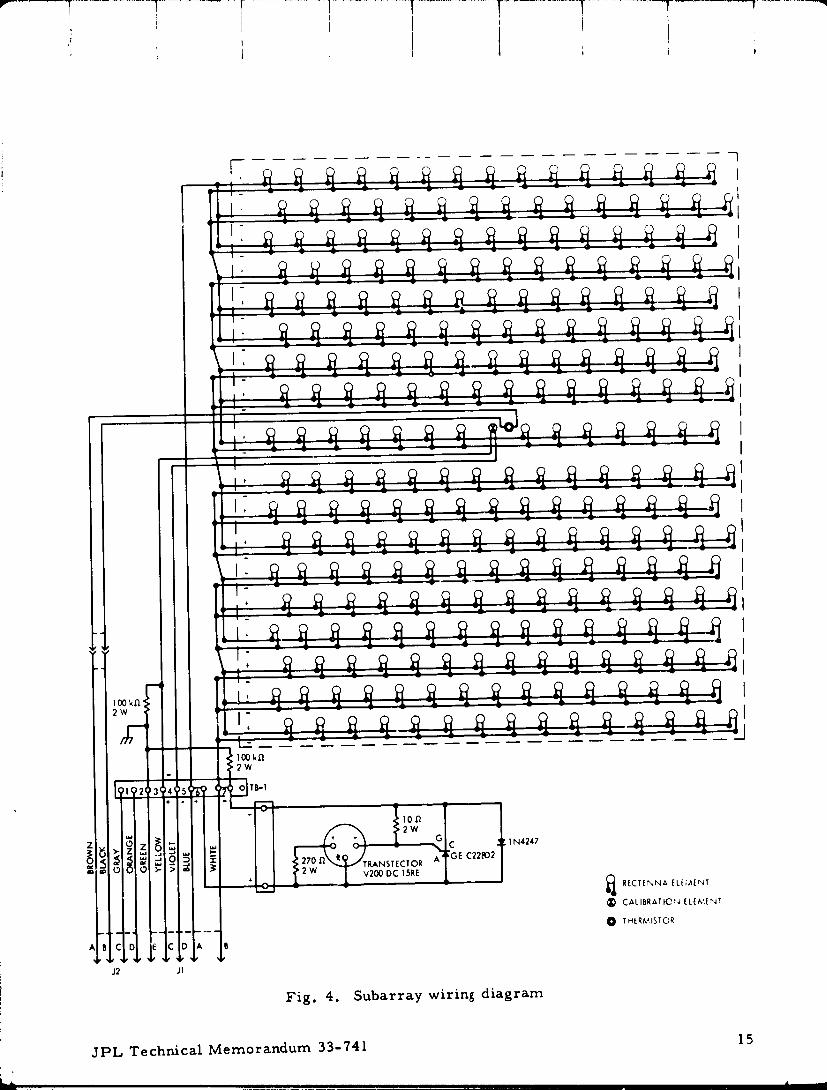
The DC wiring consists of 6 series groups of 3 each parallel-wired
horizontal rows. Each row consists of 15 parallel diodes atta hed to one
DC collection buss bar as shown in Fig. 4.
The quantity of 45 diodes in parallel in any one group was found to be
sufficient to yield a combined short circuit current that is adequate for fusing
open the 0. 025-ram (1-mil) diameter gold wires ,,sed to bond from the diode
chip to the diode package. This makes the subarray self clearing in case of
a fault. Generally the most common diode failure mechanism is a punch
through the epitaxial layer of the diode, which results in a shorted diode. The
faults are generally the result of exceeding the reverse breakdown voltage
due to excessive P.F input and/or improper (light) DC loading conditions.
Another protective feature is an overvoltage crowbar unit on the output
of the subarray. If the output voltage reaches a preset value, a short circuit
is applied via an SCR. This reduces the voltage to protect the diodes in
case of a light load condition, open circuit, or excessive RF input. The
crowbar unit is self-resetting whenever the RF input is reduced and/or the
load condition is corrected.
The subarray diodes are generally safe in a DC short condition
because the resulting RF mismatch causes most of the incident RF power to
be reflected. An open circuit load condition leads to a larse fraction of
reflected power also, but the open circuit yields high voltages at the diodes
in contrast to the short circuit condition.
The subarrays incorporate ,nechanical provisions for varying simulta-
neously the spacing between the dipoles and the ground plane.
Performance status instrumentation is provided for RF input power and
:entral buss bar temperature. The central dipole in the array is isolated
from the DC power collection buss bar and is provided with its own output
leads such that a separate load can be used to derive a sample of voltage
proportional to the incident RF power, it also has its own crowbar unit.
JPL Technical Memorandum 33-741 5
..... II I II I ......... II I I III IIIIlI .......... I ........... _ .d
1976004119-013
; i i i
The temperature data is obtained through use of ,_ thermistor element
attached to the central buss bar. The thermistor and its associated leads
are RF bypassed and shielded in order to prevent RF heating of the element.
High-impedance bleeder resistors from the DC output leads are used
to prevent charge buildup during subarray handling and storage. One side of
the DC output is grounded to the subarray frame for lightning and personnel
protection.
VI. THE ARRAY
The array is arranged in the format of three vertical columns by six
horizontal rows. The array is filled with the exception of the top central
subarray, which was deleted during the program in order to balance the
project budget,
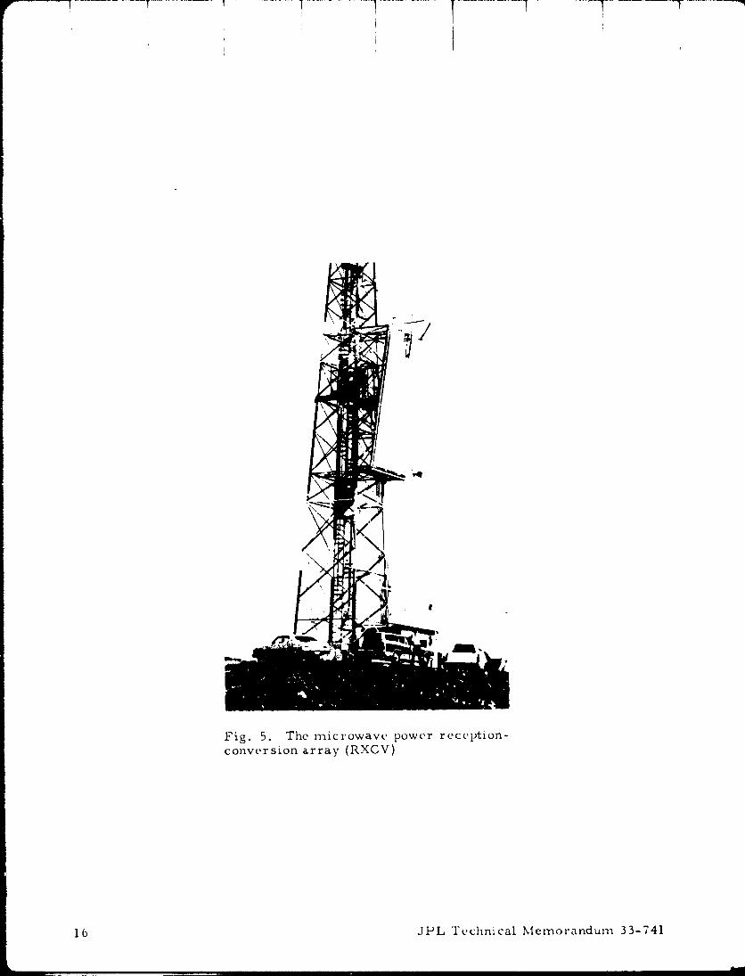
Figure 5 shows the array, which is mounted approximately half way up
the face of the existing 30.5-m (100-ft) tall collimation tower on a hill which
places the array 7 deg in elevation above the Venus Station Z6-m (85 ft)
diameter antenna. The antenna aperture to array spacing is 1.54 kin.
The tower mounting was selected so as to yield reflection free ilium-
ination patterns and also for project safety in the event of unathorized
personnel wandering unannounced and uninvited in the high-power test range.
The array physical capture area, including the interstices between
subarrays, is 24.5 m 2 (263.5 ftZ). Each of the 17 subarrays is positioned
normal to the beam from the Venus station antenna. All subarrays lie in the
same plane.
-,! VII. DC LOAD AND INSTRUMENTATION
The 17 separate DC load and instrumentation wires from each subarzav
are routed to a central load and instrumentation complex located in and near
the collimation tower support building.
+
6 JPL Technical Memorandum 33-741
........................ • i ....................... liNDI I I II
1976004119-014

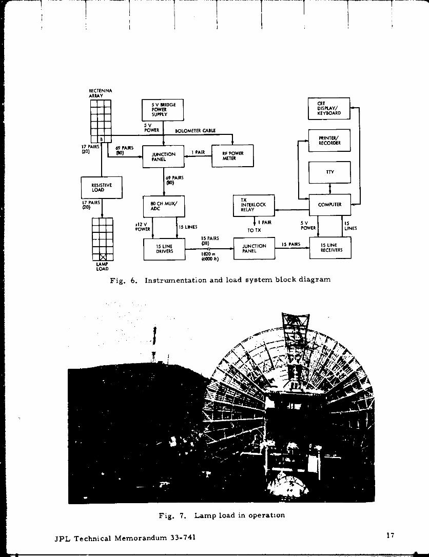
Figure 6 shows the instrumentation and load system block diagram
and indicates that the individual DC loads are each split such that approxi-
mately one third of the power is dissipated in a lamp load. The remainder
is dissipated in power resistors. Precision calibrated current shunts and
voltage dividers allow the DC power to be accurately calculated to within
a measured accuracy of ± 1/270.
The lamp loads shown in Fig. ? are structured in the same geometrical
arrangement as the power receiving array. The lamps are u: -d to indicate
visually how the RF energy density is varied across the array as the
illurrtinatingantenna is pointed over the array, yielding a one-to-one corres-
pondence that is useful in convincing people that power is indeed being
transmitted without wires.
A calibrated standard gain horn is fixed near the lower right side of
the array(Fig. 8)to provide an accurately calibrated measure of the incident
peak RF flux density. By the use of pre-programmed software and by
directing the transmit antenna beam alternately at the calibration horn and
the central isolated calibration element of each subarray, an accurate cali-
bration of the incident RF power on each subarray i_ obtained. Long-term
drifts or shifts in the diode calibration elements are thus minimized.
The calibration horn output power meter recorder output, the load
current and voltage, and the temperature data are processed iu an analog to
digital converter for transmission via a 50-pair telephone data line to the
Venus Station control room.
Figure 9 shows the data receiving and recording end of the system. A
minicomputer is used to process the subarray output voltage, current,
temperature and incident RF power data such as to provide engineering
' performance data and to provide threshold warning or automatic pre-set
shutdown via klystron drive remcval.
In addition to the data processing computer, a video quick-look data
display unit and a combination cassette tape data recorder - hard copy
printer are provided. Keyboard entry is used to command various data
display formats and to set threshold warning levels or shutdown limits.
JPL Technical Memorandum 33-741 7
........................................ 'aT
"197'6004"1"19-01,5
The data is formatted in the same 3 × 3 configuration as the subarrays
and displays for each subarray the RF input power, the output DC power,
the ratio or efficiency, the voltage and temperature of each subarray, and the
total array input RF power, DC output, and average array efficiency.
A parallel, but isolated, switch selected digital voltmeter t"_:_ ;r used
to read the individual subarray voltages and an LED array brightness display
are backup instrumentation in case of computer failure.
VIII. THE RXCV SYSTEM PERFORMANCE
The following data represents the collection of the RXCV operating
performance to date. The incident illumination distribution is shown in the
E and H-plane patterns (Figs. I0 and ll) of the 26-m antenna as measured
with the standard gain horn at the array location before subarray installation.
The power distribution was verified both via standard pattern cut) as well as
by moving the standard gain horn over the proposed subarray locations when
the transmitting antenna pointing position was held constant. Less than
0.1-dB pattern ripple was measured, indicating a clean, unobstructed
illumination.
Because of _he small size of the array relative to the 26-m-diameter
antenna tubular beam, only about II. 3_/0of the klystron transmitter o_tput is
incident on the array (see Fig. IZ) and is thus available for collection and
conversion to DC output.
Figure 13 shows the DC power output and average collection-conversion
efficiency of the array as a function of the incident peak I_F flux density for
the illuminating beam centered at the geometrical center of the array. The
efficiency remains high over a large range of input power levels. As yet,
the maximum efficiency operating point has not yet been reached. Figure 14
shows an estimated power balance diagram for a typical subarray.
Because of the partial lamp load, the total subarray load resistance
varies with power level, as shown in Fig. 15. .Also shown is the output
voltage variation,
8 3PL Technical Memorandum 33-741
I II IIII I II IIII III I,, I 2 " :, ................ 1I I I Ill I I
1.qT Rnndl lo_n

P i i j
Figure 16 shows the results of an experiment to determine the array
efficiency as a function of temperature. The thermal time constant of the
subarray is approximately 16 minutes with an 8°C rise for operation at the
design point. The low temperature rise reflects the high diode conversion
efficiency and good heat sinking of the diodes.
Table 1 shows the statistical performance of the 17 subarrays for
similar incident power conditions.
Figure 17 shows the subarray collection-conversion efficiency for
various load conditions.
Figure 18 illustrates the usefulness of the modules of the array in
determining the illumination beam peak pointing position. By subdividing
the array as shown in the inset figures and performing the subarray output
sum and di.ffea'ence power ratios relative to the respective reference lines,
the resulting 'lmonopulse" pointing data may be generated. Allowing for the
variations in subarray off-axis biases and variations with power level, ".he
beam center can be reliably located to within approximately 1/30 of a beam-
width in the current case.
Figure 19 shows the short circuit load current performance of a
subarray.
After accumulating approximately 65 total hours of operation at vari-
ous power levels, the array was checked for failed diodes on Aug. 20, 1975.
Out of the total of 4,590 diodes, only 18 diodes were faulted.
The failed diodes will be examined in an attempt to determine the cause
of failure. However, it is known that the diodes were subjected to greater
than ._ormal design level RF intensity in the course of this initial checking of
the system.
IX. CONCLUSIONS AND RECOMMENDATIONS
Over 30 kW of DC output power has been transmitted a distance of
1.54 km without wires. The ratio of total DC output to integrated total
available incident RF power on the reception-conversion array was greater
than 80%.
2PL Technical Memorandum 33-741 9
,,, ....................................... , , , , ...... .................................................
1976004119-017

In order to improve the product, higher conversion efficiency diodes,
better array impedance match, and mass-manufacturing simplicity of design
for easier fabrication and assembly will be necessary.
Additional parameter variation tests are planned in the future to deter-
mine the performance versus frequency, incident polarization, treatment of
the interstices, and various environmental conditions--including rain, snow,
and angle of incidence variations.
In summary then, the present rectenna array Concept should be adequate
to provide a somewhat weather-dependent, yet highly efficient receiving mech-
anizatior, for a high-power microwave power transmission link.
U 10 JPL Technical Memorandum 33-741.... _ ni]i II _-- , ...... _ ....... i "' ' "' ........................................ illll IF II ....................................................................... q
1976004119-018

REFERENCES
1. O'Neill, J.J., Prodisal Genius, The Life of Nikola Testa, IvesWashburn, Inc., N.Y., 1944
2. Hunt, I., and Draper, W., Lightning in His Hand, The Life Story ofNiko!a Tesla, Sage Books, Denver, 1964.
3. Dickinson, R., and Brown, W., Radiated Microwave Power
Transmission System Efficiency Measurements, TechnicalMemorandum 33-7Z7, Jet Propulsion Laboratory, Pasadena, Calif.,
May 15, 1975.
4. Brown, W., "The Technology and Application of Free-Space PowerTransmission by Microwave Beam," in IEEE Proceedings, Vol. 6Z,
No. I, pp. II-ZS, January 1974.
t
• i JPL Technical Memorandum 33-741 11
1976004119-019

O
°e=l
Q; N 0
•g, ,_N
U
U
aO _
OI
NN
,.Q
al
t-- i_
-- _ ,.o o_ m oo oP
0
N
P,
N%
g
0 0 u 0
_ o o
12 JPL TechnicalMemorandum 33-741
A.................................... IIIIIIIIIII II |
1976004119-020

Fig. i. The Venus station gO-,n antunna and collimation tow,'r
JPL Tt, chnical Memorandum 33-741 1
1976004119-021

IT T i °AB_,*,k I[ R B', PA','_DIODt CAPACITOr,
_ ._ [
_AfBAL,'_rJC[ ['_j I At_ ,MI I(_r,["IPtq.t I ;,.4 Le...
I p_, fIill_.
14 .11'I, [,'_t_l'.!c:,l ._l,,1_._,t',_i,._t';:,,,, _ _-7.11
k . m m I mill m I
1976004119-022
I N4247
A _ C22R32 "ITRANSTECTORV200 DC ISRE
(_) CALIBRATIO_ [L{&',E_'4T
0 T HtR&'qSTOR
A
J2 JI
Fig. 4. Subarray wiring diagram
3PL Technical Memorandum 33-741 15
hA
............. | I I
1976004 ] ] 9-023
T l T l T, "T ",II *
\\
Fig. 5. The microwave power reception-conversion array (RXCV)
16 JPL Technical Memorandum 33-741
1976004119-024
RECTENNAARRAY
5 V RIDGE CRT
-iSUPPLY KEYBOARD
POWER BOLOMETER CABLE
PRINTER/-- RECORDER
17 PAIRSJ 69 PAIRS [ [
(zo) _o) _ +PAIR [JUNCTION RF POWERPANEL _ METER
I L+L J "'+ ,RESISTIVELOAD
17 PAIRS 80 CH MUX/ INTERLOCK COMPUTER(20) ADC RELAY
*+i +I I +l !,+POWER 15 LINES TO TX
15 PAIRS
15 LINE (38) 15 PAIRSp,_ _ JUNCTION _ 15 LINEDRIVERS 1820 m PANEL RECEIVERS
(6ooo_)LAMPLOAD
Fig. 6. Instrumentation and load system block diagram
Fig. 7. Lamp load in operation
JPL Technical Memorandum 33-741 17
Jk
I
1976004119-025

T T T ! T F T r "_
' I
Fig. 8. RXCV array and fieldstrength calibrationhorn
18 JPL T(,chnical Memorandum 33-741
1976004119-026

1976004119-027

, r..........................1 l 1 , "I I / | i
_, : J
' 7//1 0.5 1.0
i.o o. _]
8
.._ IO. 2
6 VENU8 /DSS-13 LINEAR \ 4
20 /POLARIZED t -41
I /COLLIMATION/T_ER / !
EL / ]6i2.s 2.0 1.5 1.o o.s o o.s 1.o
AN_t.E e deg
Fig. I0. g6-m antenna near fieldelevation pattern
- ---T----------_
,;o 0.5/'_\ 0.5 ,.o
.. ,o__ 4
_. / VENUS STATIONb M / DSS-i3 LINEAR Ie / \ ] POLARIZED I
20 / 7 PATTERNAT l
' A/ TOWER "'X /\6
' it 3O246 l i , I l
2.0 1.5 1.0 0.5 0 0.5 1.0 1.5 2.0
ANGLE, de9
Fig. II. Z6-m antenna near fieldazimuthpattern
JPL Technical Memorandum 33-741:r Z0
1976004119-028

1-46 CONTOURS
Fig. IZ. l-dB incident beam contours
30 I I I I I I I
_. 25- -_
_ 2o-- - 8o_-x _" _
'qcc/ / z
' _u 15- /////,/'-r0x/ 750_"'z
._ zx_ o
0
0 I I I I I I _ u0 25 50 75 100 125 150 ! 75
INCIDENT PEAK RF FLUX DENSITY, mW/cm2
Fig. 13. Microwave high-power reception-
conversion array performance
JPL Technical Memorandum 33-741 Zl
................ i -- ....... jill l,,I l ' [ Jlllli ...........................
1976004119-029

245 W WAST_ HEATI1% DIODECONVERSION LOSS
_R LOSSES
IAVAILABLE SUBARRAY_ow,.i _ \,_ i \!
1869 WDC OUTPUT
MISMATCH _ / 84%HARMONIC _. /
Fig. 14. Subarray power balance diagramfor 16Z mg/cm Z peak RF incident flux
density
a 200 I I I i I I 20
u,,,, 15
> m
100 _10
o 1 I I I I I 0 :_0 25 50 75 100 125 150 175 '_
INCIDENT PEAK RF F:UX DENSITY, mW/_ 2
Fig. 15. Subarray output voltage and loadcharacteristics
ZZ JPL Technical Memorandum 33-741
.... -- ........ _=_,1,., , ii ................................................ ilia ii ................................................ . .... _,_ .,., -_-1 _
1976004119-030

- T ] l ] -T' t i.t i ; i' i
zz'°_851-' ' .... ' 1
°-°"U_Z Lu'l>_ / oeeeo oe • • • •
00_ /
UUu_ 79[- t , I , , , , , 1
ou 4b 1 1 I ' !
g_,o-
U_ _U
>- _ 35 N,%
_ 30""_ X ENSIT 130mW/cm 2 t
m_ 25 D Y OFF I30 4o so l_:oo Io 20 30 4'o 5'o 14:oolO
TIME, min
Fig. 16. Subarray performance variationversus temperature
1.0 I I I I
_;,._Z0.8 _4i-"_',d,,=-u,J
Z 0.6 --9uJ>Zou 0.4Z_o
u 0.2
1 I I I4 8 12 16 20
LOAD RESISTANCE, .fl
Fig. 17. Collection conversion efficiencyversus load resistance for 130 mW/cm 2
peak incident RF power
[
5PL Technical Memorandum 33-741 Z3%
1976004119-031

t ........... W .......... _
I !
oo°53omw2o2°313ow2,/ / _ '_w'_2
0.05 0.I -
.-o.o5 _ ,..;"-0.1
-0.I0 -0.2
REF.
-o.15 1 [ I I i I -0.3t I. [ I l I I J260.46 .48 .50 .52 .54 .56 .58 .60 6.95 7.0 .05 .1O .15 .20 .25 .30
STATION AZ)he/TH READOUT, deg STATJON ELEVATION READOUT, deg
Fig. 18. Monopulse pointing performance, microwave power
transmission reception-conversion array
I ! I I I I
16
'_ 12_=.
Z
_J
_ 8
4
I I [ I I I0 25 50 75 100 125 150 175
PEAK RF FLUX DENSITY, mW/cm 2
!i Fig. 19. Short circuit load performance_ of a subarray
_C
_, Z4 JPL Technical Memorandum 33-741
NASA -- JP[ - Coral., I.A., CajUn.
| ....I II I, I I II I
1976004119-03P