Embed Size (px)
Citation preview
General DescriptionThe MAX5732–MAX5735 are 32-channel, 16-bit, voltage-output, digital-to-analog converters (DACs). All devicesaccept a 3V external reference input. The devicesinclude an internal offset DAC that allows all the outputsto be offset and a ground-sensing function, allowing out-put voltages to be referenced to a remote ground.
A 33MHz SPI™-/QSPI™-/MICROWIRE™- and digitalsignal processor (DSP)-compatible serial interface con-trols the MAX5732–MAX5735. Each DAC has a double-buffered input structure that helps minimize the digitalnoise feedthrough from the digital inputs to the outputs,and allows for synchronous or asynchronous updatingof the outputs. The MAX5732–MAX5735 also provide aDOUT that allows for read-back or daisy chaining multi-ple devices. The devices provide separate powerinputs for the analog and digital sections and provideseparate power inputs for the output buffer amplifiers.The MAX5732–MAX5735 include proprietary deglitchcircuits to prevent output glitches at power-up andeliminate the need for power sequencing. The devicesprovide a software-shutdown mode to allow efficientpower management. The MAX5732–MAX5735 con-sume 50µA of supply current in shutdown.
The MAX5732–MAX5735 provide buffered outputs thatcan drive 10kΩ in parallel with 100pF. The MAX5732 hasa 0 to +5V output range; the MAX5733 has a 0 to +10Vrange; the MAX5734 has a -2.5V to +7.5V range; theMAX5735 has a -5V to +5V range. The MAX5732–MAX5735 are available in a 56-pin, 8mm x 8mm, thinQFN package and 64-pin TQFP package and operateover the 0°C to +85°C temperature range.
ApplicationsAutomatic Test Systems
Optical Router Controls
Industrial Process Controls
Arbitrary Function Generators
Avionics Equipment
Digital Offset/Gain Adjustment
Features ♦ Guaranteed Monotonic to 16 Bits♦ 32 Individual DACs in an 8mm x 8mm, 56-Pin,
Thin QFN Package or 64-Pin TQFP Package♦ Four Output Voltage Ranges
0 to +5V (MAX5732)0 to +10V (MAX5733)-2.5V to +7.5V (MAX5734)-5V to +5V (MAX5735)
♦ Buffered Voltage Outputs Capable of Driving10kΩ || 100pF
♦ Glitch-Free Power-Up♦ SPI-/QSPI-/MICROWIRE-/DSP-Compatible 33MHz
Serial Interface
MA
X5
73
2–M
AX
57
35
32-Channel, 16-Bit, Voltage-Output DACs with Serial Interface
________________________________________________________________ Maxim Integrated Products 1
Ordering Information
19-3148; Rev 7; 11/05
For pricing, delivery, and ordering information, please contact Maxim/Dallas Direct! at 1-888-629-4642, or visit Maxim’s website at www.maxim-ic.com.
EVALUATION KIT
AVAILABLE
PARTOUTPUT
VOLTAGE(V)
MAXINL
(LSB)
PIN-PACKAGE
PKGCODE
MAX5732AUTN 0 to +5 ±856 ThinQFN-EP*
T5688-3
MAX5732BUTN 0 to +5 ±1656 ThinQFN-EP*
T5688-3
SPI/QSPI are trademarks of Motorola, Inc.
MICROWIRE is a trademark of National Semiconductor Corp.
Pin Configurations continued at end of data sheet.
Note: All devices operate over the 0°C to +85°C temperaturerange.*EP = Exposed pad (internally connected to VSS).
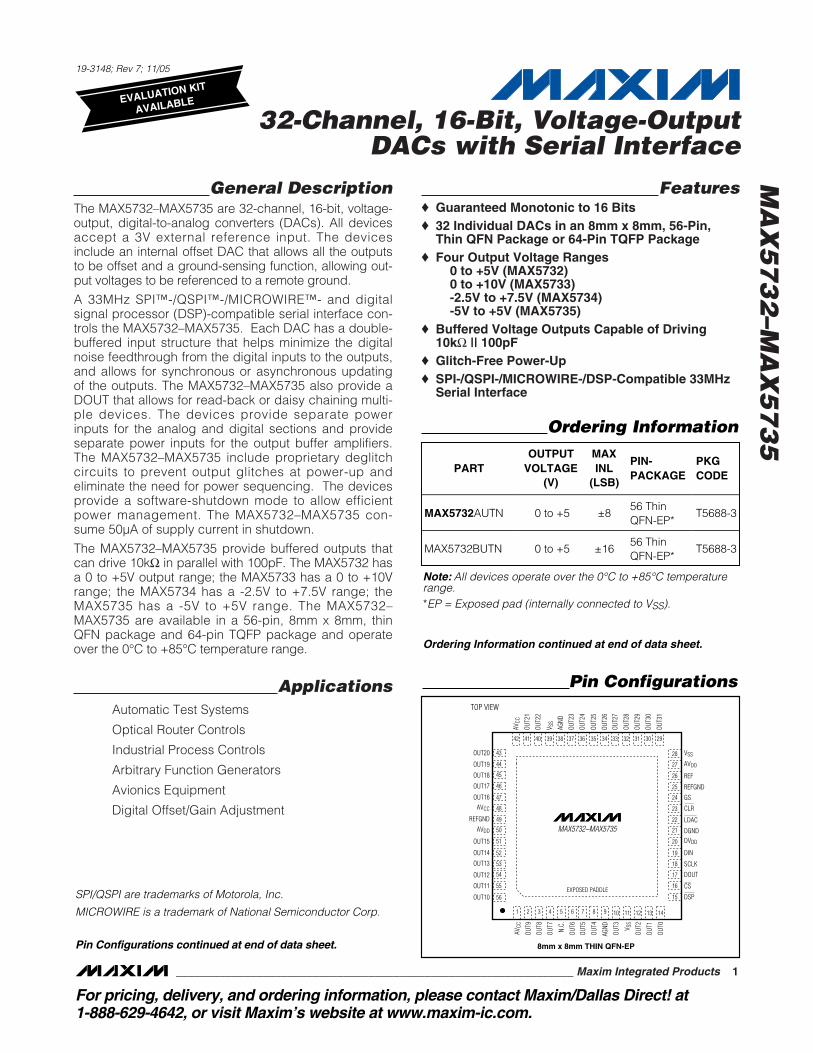
TOP VIEW
MAX5732–MAX5735
V SS
OUT3
AGND
OUT4
OUT5
OUT6
OUT0
OUT1
OUT2
N.C.
OUT7
OUT8
OUT9
AVCC
111098765432 1413121
EXPOSED PADDLE CS
8mm x 8mm THIN QFN-EP
DSP
SCLK
DOUT
DVDD
DIN
LDAC
DGND
GS
CLR
REF
REFGND
VSS
AVDD
20
19
18
17
16
24
23
22
21
15
26
25
28
27
29303132333435363738
AGND
OUT2
3
OUT2
4
OUT2
5
OUT2
6
OUT2
7
OUT2
8
OUT2
9
OUT3
0
OUT3
1
39
V SS
4041
OUT2
1
OUT2
2
42
AVCC
46
47
48
49
50
43
44
45
51OUT15
AVDD
REFGND
AVCC
OUT16
OUT17
OUT18
OUT19
OUT20
52OUT14
53
54
55OUT11
OUT12
OUT13
56OUT10
Pin Configurations
Ordering Information continued at end of data sheet.
MA
X5
73
2–M
AX
57
35
32-Channel, 16-Bit, Voltage-Output DACs with Serial Interface
2 _______________________________________________________________________________________
ABSOLUTE MAXIMUM RATINGS
ELECTRICAL CHARACTERISTICS—MAX5732 (0 to +5V Output Voltage Range)(AVCC = +5.25V to +5.5V (Note 1), AVDD = +5V ±5%, DVDD = +2.7V to AVDD, VSS = AGND = DGND = REFGND = GS = 0, VREF =+3.0V, RL = ∞, CL = 50pF referenced to ground, TA = TMIN to TMAX, unless otherwise noted. Typical values are at TA = +25°C.)
Stresses beyond those listed under “Absolute Maximum Ratings” may cause permanent damage to the device. These are stress ratings only, and functionaloperation of the device at these or any other conditions beyond those indicated in the operational sections of the specifications is not implied. Exposure toabsolute maximum rating conditions for extended periods may affect device reliability.
AVCC to VSS, AGND, DGND, REFGND..................-0.3V to +12VVSS to AGND, DGND................................................-6V to +0.3VAVDD, DVDD to AGND, DGND, REFGND.................-0.3V to +6VAGND to DGND.....................................................-0.3V to +0.3VREF to AGND, DGND,
REFGND...............-0.3V to the lower of (AVDD + 0.3V) and +6VREFGND to AGND.................................................-0.3V to +0.3VDigital Inputs to AGND, DGND,
REFGND..............-0.3V to the lower of (DVDD + 0.3V) and +6VDOUT to DGND.......-0.3V to the lower of (DVDD + 0.3V) and +6VOUT_ to VSS.........-0.3V to the lower of (AVCC + 0.3V) and +12VGS to AGND ................................................................-1V to +1V
Maximum Current into REF...............................................±10mAMaximum Current into Any Pin .........................................±50mAContinuous Power Dissipation (TA = +70°C)
Thin QFN (derate 31.3mW/°C above +70°C)...................2.5WTQFP (derate 25mW/°C above +70°C)............................2.0W
Operating Temperature RangesMAX573__UCB ...................................................0°C to +85°C
Junction Temperature ......................................................+150°CStorage Temperature Range .............................-65°C to +150°CLead Temperature (soldering, 10s) .................................+300°C
PARAMETER SYMBOL CONDITIONS MIN TYP MAX UNITS
DC CHARACTERISTICS
Resolution N 16 Bits
MAX5732A ±4 ±8Integral Nonlinearity (Note 2) INL
MAX5732B ±8 ±16LSB
Differential Nonlinearity DNL Guaranteed monotonic (Note 3) ±1 LSBZero-Scale Error VOS VSS = -0.5V, AVCC = +5.25V (Note 4) ±8 ±40 mV
Full-Scale Error (Note 4) ±8 ±50 mV
Gain Error ±0.1 ±0.5 %FSR
Gain Temperature Coefficient 20ppm
FSR/°C
DC Crosstalk VSS = -0.5V, AVCC = +5V (Note 5) 50 250 µV
DYNAMIC CHARACTERISTICS
Output-Voltage Settling Time Full-scale change to ±0.5 LSB 20 µs
Voltage-Output Slew Rate 1 V/µs
Digital Feedthrough (Note 6) 5 nV-s
Digital Crosstalk (Note 7) 5 nV-s
Digital-to-Analog Glitch Impulse Major carry transition 120 nV-s
DAC-to-DAC Crosstalk (Note 8) 15 nV-s
Output Noise Spectral Density at1kHz
Full-scale code 250 nV/√Hz
ANALOG OUTPUTS (OUT0 to OUT31)
Output Voltage Range VSS = -0.5V, AVCC = +5.25V (Note 1) 0 5 V
Resistive Load to Ground 10 50 kΩ
MA
X5
73
2–M
AX
57
35
32-Channel, 16-Bit, Voltage-Output DACs with Serial Interface
_______________________________________________________________________________________ 3
ELECTRICAL CHARACTERISTICS—MAX5732 (0 to +5V Output Voltage Range) (continued)(AVCC = +5.25V to +5.5V (Note 1), AVDD = +5V ±5%, DVDD = +2.7V to AVDD, VSS = AGND = DGND = REFGND = GS = 0, VREF =+3.0V, RL = ∞, CL = 50pF referenced to ground, TA = TMIN to TMAX, unless otherwise noted. Typical values are at TA = +25°C.)
PARAMETER SYMBOL CONDITIONS MIN TYP MAX UNITS
Capacitive Load to Ground 50 100 pF
DC Output Impedance 0.1 Ω
Sourcing, full-scale code, output connectedto AGND
5
Short-Circuit CurrentSinking, zero-scale code, output connectedto AVCC
-5
mA
GROUND-SENSE ANALOG INPUT (GS)
Input Voltage Range VGS Relative to AGND -0.5 +0.5 V
GS Gain AGS 0.995 1.000 1.005 V/V
Input Resistance -0.5V ≤ VGS ≤ +0.5V, VSS = -0.5V 35 kΩREFERENCE INPUT (REF)
Input Resistance 1 MΩReference Input Voltage Range VREF Referred to REFGND 2.900 3.000 3.100 V
DIGITAL INPUTS (CS, SCLK, DIN, LDAC, CLR, DSP)
DVDD = +2.7V to +3.6V0.7 ×DVDDInput-Voltage High VIH
DVDD = +4.75V to +5.25V 2.4
V
Input-Voltage Low VIL 0.8 V
Input Capacitance CIN 10 pF
Input Current IIN Digital inputs = 0 or DVDD ±1 µA
POWER REQUIREMENTS (AVCC, VSS, AGND, AVDD, DVDD, DGND)
Output-Amplifier Positive SupplyVoltage
AVCC (Note 1) 4.75 5.50 V
Output-Amplifier Negative SupplyVoltage
VSS -0.5 0 V
Output-Amplifier Supply VoltageDifference
AVCC - VSS 5.75 V
Analog Supply Voltage AVDD 4.75 5.25 V
Digital Supply Voltage DVDD 2.70 5.25 V
VOUT0 through VOUT31 = 0 10 15 mAAnalog Supply Current AIDD
Software shutdown 10 µA
VIH = DVDD, VIL = 0, fSCLK = 20MHz 2.5 3.5Digital Supply Current DIDD
VIH = +2.4V, VIL = +0.8V, fSCLK = 20MHz 5 6.5mA
VOUT0 through VOUT31 = 0 4 10 mAOutput-Amplifier Positive SupplyCurrent
AICCSoftware shutdown 20 µA
VOUT0 through VOUT31 = 0 -4 -10 mAOutput-Amplifier Negative SupplyCurrent
ISS VSS = -0.5VSoftware shutdown -20 µA
Power-Supply Rejection Ratio PSRR -95 dB
MA
X5
73
2–M
AX
57
35
32-Channel, 16-Bit, Voltage-Output DACs with Serial Interface
4 _______________________________________________________________________________________
ELECTRICAL CHARACTERISTICS—MAX5733 (0 to +10V Output Voltage Range)(AVCC = +10.5V to +11V, AVDD = 5V ±5%, DVDD = +2.7V to AVDD, VSS = AGND = DGND = REFGND = GS = 0, VREF = +3.0V, RL = ∞, CL = 50pF referenced to ground, TA = TMIN to TMAX, unless otherwise noted. Typical values are at TA = +25°C.)
PARAMETER SYMBOL CONDITIONS MIN TYP MAX UNITS
DC CHARACTERISTICS
Resolution N 16 Bits
MAX5733A ±4 ±8Integral Nonlinearity (Note 2) INL
MAX5733B ±8 ±16LSB
Differential Nonlinearity DNL Guaranteed monotonic (Note 3) ±1 LSB
Zero-Scale Error VOS VSS = -0.5V, AVCC = +10V (Note 4) ±8 ±40 mV
Full-Scale Error (Note 4) ±8 ±50 mV
Gain Error ±0.1 ±0.5 % FSR
Gain Temperature Coefficient 20ppm
FSR/°C
DC Crosstalk VSS = -0.5V, AVCC = +10V (Note 5) 50 250 µV
DYNAMIC CHARACTERISTICS
Output-Voltage Settling Time Full-scale change to ±0.5 LSB 20 µs
Voltage-Output Slew Rate 1 V/µs
Digital Feedthrough (Note 6) 5 nV-s
Digital Crosstalk (Note 7) 5 nV-s
Digital-to-Analog Glitch Impulse Major carry transition 120 nV-s
DAC-to-DAC Crosstalk (Note 8) 15 nV-s
Output Noise Spectral Density at1kHz
Full-scale code 250 nV/√Hz
ANALOG OUTPUTS (OUT0 to OUT31)
Output Voltage Range VSS = -0.5V, AVCC = +10.5V (Note 1) 0 10 V
Resistive Load to Ground 10 50 kΩCapacitive Load to Ground 50 100 pF
DC Output Impedance 0.1 Ω
Sourcing, full scale, output connected toAGND
5
Short-Circuit CurrentSinking, zero scale, output connected toAVCC
-5
mA
GROUND-SENSE ANALOG INPUT (GS)
Input Voltage Range VGS Relative to AGND -0.5 +0.5 V
GS Gain AGS 0.995 1.000 1.005 V/V
Input Resistance -0.5V ≤ VGS ≤ +0.5V, VSS = -0.5V 70 kΩREFERENCE INPUT (REF)
Input Resistance 1 MΩReference Input Voltage Range VREF Referred to REFGND 2.900 3.000 3.100 V

MA
X5
73
2–M
AX
57
35
32-Channel, 16-Bit, Voltage-Output DACs with Serial Interface
_______________________________________________________________________________________ 5
ELECTRICAL CHARACTERISTICS—MAX5733 (0 to +10V Output Voltage Range) (continued)(AVCC = +10.5V to +11V, AVDD = 5V ±5%, DVDD = +2.7V to AVDD, VSS = AGND = DGND = REFGND = GS = 0, VREF = +3.0V, RL = ∞, CL = 50pF referenced to ground, TA = TMIN to TMAX, unless otherwise noted. Typical values are at TA = +25°C.)
PARAMETER SYMBOL CONDITIONS MIN TYP MAX UNITS
DIGITAL INPUTS (CS, SCLK, DIN, LDAC, CLR, DSP)
DVDD = +2.7V to +3.6V0.7 ×DVDDInput-Voltage High VIH
DVDD = +4.75V to +5.25V 2.4
V
Input-Voltage Low VIL 0.8 V
Input Capacitance CIN 10 pF
Input Current IIN Digital inputs = 0 or DVDD ±1 µA
POWER REQUIREMENTS (AVCC, VSS, AGND, AVDD, DVDD, DGND)
Output-Amplifier Positive SupplyVoltage
AVCC (Note 1) 10 11 V
Output-Amplifier Negative SupplyVoltage
VSS -0.5 0 V
Output-Amplifier Supply VoltageDifference
AVCC - VSS 11 V
Analog Supply Voltage AVDD 4.75 5.25 V
Digital Supply Voltage DVDD 2.70 5.25 V
VOUT0 through VOUT31 = 0 10 15 mAAnalog Supply Current AIDD
Software shutdown 10 µA
VIH = DVDD, VIL = 0, fSCLK = 20MHz 2.5 3.5Digital Supply Current DIDD
VIH = +2.4V, VIL = +0.8V, fSCLK = 20MHz 5 6.5mA
VOUT0 through VOUT31 = 0 4 10 mAOutput-Amplifier Positive SupplyCurrent
AICCSoftware shutdown 20 µA
VOUT0 through VOUT31 = 0 -4 -10 mAOutput-Amplifier Negative SupplyCurrent
ISS VSS = -0.5VSoftware shutdown -20 µA
Power-Supply Rejection Ratio PSRR -95 dB
MA
X5
73
2–M
AX
57
35
32-Channel, 16-Bit, Voltage-Output DACs with Serial Interface
6 _______________________________________________________________________________________
ELECTRICAL CHARACTERISTICS—MAX5734 (-2.5V to +7.5V Output Voltage Range)(AVCC = +7.75V to +8.25V, AVDD = +5V ±5%, DVDD = +2.7V to AVDD, VSS = -2.75V to -3.25V, AGND = DGND = REFGND = GS = 0,program the offset DAC to 4000hex. VREF = +3.0V, RL = ∞, CL= 50pF referenced to ground, TA = TMIN to TMAX, unless otherwisenoted. Typical values are at TA = +25°C.)
PARAMETER SYMBOL CONDITIONS MIN TYP MAX UNITS
DC CHARACTERISTICS
Resolution N 16 Bits
MAX5734A ±4 ±8Integral Nonlinearity (Note 2) INL
MAX5734B ±8 ±16LSB
Differential Nonlinearity DNL Guaranteed monotonic (Note 3) ±1 LSBZero-Scale Error VOS VSS = -3.25V, AVCC = +7.75V (Note 4) ±8 ±40 mV
Full-Scale Error (Note 4) ±8 ±50 mV
Gain Error ±0.1 ±0.5 %FSR
Gain Temperature Coefficient 20ppm
FSR/°C
DC Crosstalk VSS = -3.25V, AVCC = +7.75V (Note 4) 50 250 µV
DYNAMIC CHARACTERISTICS
Output-Voltage Settling Time Full-scale change to ±0.5 LSB 20 µs
Voltage-Output Slew Rate 1 V/µs
Digital Feedthrough (Note 6) 5 nV-s
Digital Crosstalk (Note 7) 5 nV-s
Digital-to-Analog Glitch Impulse Major carry transition 120 nV-s
DAC-to-DAC Crosstalk (Note 8) 15 nV-s
Output Noise Spectral Density at1kHz
Full-scale code 250 nV/√Hz
ANALOG OUTPUTS (OUT0 to OUT31)
Output Voltage Range VSS = -2.75V, AVCC = +7.75V (Note 1) -2.5 +7.5 V
Resistive Load to Ground 10 50 kΩCapacitive Load to Ground 50 100 pF
DC Output Impedance 0.1 Ω
Sourcing, full scale, output connected toAGND
5
Short-Circuit CurrentSinking, zero scale, output connected toAVCC
-5
mA
GROUND-SENSE ANALOG INPUT (GS)
Input Voltage Range VGS Relative to AGND -0.5 +0.5 V
GS Gain AGS 0.995 1.000 1.005 V/V
Input Resistance -0.5V ≤ VGS ≤ +0.5V, VSS = -0.5V 70 kΩREFERENCE INPUT (REF)
Input Resistance 1 MΩReference Input Voltage Range VREF Referred to REFGND 2.900 3.000 3.100 V
MA
X5
73
2–M
AX
57
35
32-Channel, 16-Bit, Voltage-Output DACs with Serial Interface
_______________________________________________________________________________________ 7
ELECTRICAL CHARACTERISTICS—MAX5734 (-2.5V to +7.5V Output Voltage Range)(continued)(AVCC = +7.75V to +8.25V, AVDD = +5V ±5%, DVDD = +2.7V to AVDD, VSS = -2.75V to -3.25V, AGND = DGND = REFGND = GS = 0,program the offset DAC to 4000hex. VREF = +3.0V, RL = ∞, CL= 50pF referenced to ground, TA = TMIN to TMAX, unless otherwisenoted. Typical values are at TA = +25°C.)
PARAMETER SYMBOL CONDITIONS MIN TYP MAX UNITS
DIGITAL INPUTS (CS, SCLK, DIN, LDAC, CLR, DSP)
DVDD = +2.7V to +3.6V0.7 ×DVDDInput-Voltage High VIH
DVDD = +4.75V to +5.25V 2.4
V
Input-Voltage Low VIL 0.8 V
Input Capacitance CIN 10 pF
Input Current IIN Digital inputs = 0 or DVDD ±1 µA
POWER REQUIREMENTS (AVCC, VSS, AGND, AVDD, DVDD, DGND)
Output-Amplifier Positive SupplyVoltage
AVCC (Note 1) 7.50 8.25 V
Output-Amplifier Negative SupplyVoltage
VSS -3.25 -2.50 V
Output-Amplifier Supply VoltageDifference
AVCC - VSS 11 V
Analog Supply Voltage AVDD 4.75 5.25 V
Digital Supply Voltage DVDD 2.70 5.25 V
VOUT0 through VOUT31 = 0 10 15 mAAnalog Supply Current AIDD
Software shutdown 10 µA
VIH = DVDD, VIL = 0, fSCLK = 20MHz 2.5 3.5Digital Supply Current DIDD
VIH = +2.4V, VIL = +0.8V, fSCLK = 20MHz 5 6.5mA
VOUT0 through VOUT31 = 0 4 10 mAOutput-Amplifier Positive SupplyCurrent
AICCSoftware shutdown 20 µA
VOUT0 through VOUT31 = 0 -4 -10 mAOutput-Amplifier Negative SupplyCurrent
ISS VSS = -2.75VSoftware shutdown -20 µA
Power-Supply Rejection Ratio PSRR -95 dB

MA
X5
73
2–M
AX
57
35
32-Channel, 16-Bit, Voltage-Output DACs with Serial Interface
8 _______________________________________________________________________________________
ELECTRICAL CHARACTERISTICS—MAX5735 (-5V to +5V Output Voltage Range)(AVCC = +5.25V to +5.5V, AVDD = +5V ±5%, DVDD = +2.7V to AVDD, VSS = -5.25V to -5.5V, AGND = DGND = REFGND = GS = 0,program the offset DAC to 8000hex. VREF = +3.0V, RL = ∞, CL = 50pF referenced to ground, TA = TMIN to TMAX, unless otherwisenoted. Typical values are at TA = +25°C.)
PARAMETER SYMBOL CONDITIONS MIN TYP MAX UNITS
DC CHARACTERISTICS
Resolution N 16 Bits
MAX5735A ±4 ±8Integral Nonlinearity (Note 2) INL
MAX5735B ±8 ±16LSB
Differential Nonlinearity DNL Guaranteed monotonic (Note 3) ±1 LSB
Zero-Scale Error VOS VSS = -5.25V, AVCC = +5.25V (Note 4) ±8 ±40 mV
Full-Scale Error (Note 4) ±8 ±50 mV
Gain Error ±0.1 ±0.5 %FSR
Gain Temperature Coefficient 20ppm
FSR/°C
DC Crosstalk VSS = -5.75V, AVCC = +5.25V (Note 5) 50 250 µV
DYNAMIC CHARACTERISTICS
Output-Voltage Settling Time Full-scale change to ±0.5 LSB 20 µs
Voltage-Output Slew Rate 1 V/µs
Digital Feedthrough (Note 6) 5 nV-s
Digital Crosstalk (Note 7) 5 nV-s
Digital-to-Analog Glitch Impulse Major carry transition 120 nV-s
DAC-to-DAC Crosstalk (Note 8) 15 nV-sOutput Noise Spectral Density at1kHz
Full-scale code 250 nV/√Hz
ANALOG OUTPUTS (OUT0 through OUT31)
Output Voltage Range VSS = -5.25V, AVCC = +5.25V (Note 1) -5 +5 V
Resistive Load to Ground 10 50 kΩCapacitive Load to Ground 50 100 pF
DC Output Impedance 0.1 Ω
Sourcing, full scale, output connected toAGND
5
Short-Circuit CurrentSinking, zero scale, output connected toAVCC
-5
mA
GROUND-SENSE ANALOG INPUT (GS)
Input Voltage Range VGS Relative to AGND -0.5 +0.5 V
GS Gain AGS 0.995 1.000 1.005 V/V
Input Resistance -0.5V ≤ VGS ≤ +0.5V, VSS = -0.5V 70 kΩREFERENCE INPUT (REF)
Input Resistance 1 MΩReference Input Voltage Range VREF Referred to REFGND 2.900 3.000 3.100 V

MA
X5
73
2–M
AX
57
35
32-Channel, 16-Bit, Voltage-Output DACs with Serial Interface
_______________________________________________________________________________________ 9
ELECTRICAL CHARACTERISTICS—MAX5735 (-5V to +5V Output Voltage Range) (continued)(AVCC = +5.25V to +5.5V, AVDD = +5V ±5%, DVDD = +2.7V to AVDD, VSS = -5.25V to -5.5V, AGND = DGND = REFGND = GS = 0,program the offset DAC to 8000hex. VREF = +3.0V, RL = ∞, CL = 50pF referenced to ground, TA = TMIN to TMAX, unless otherwisenoted. Typical values are at TA = +25°C.)
PARAMETER SYMBOL CONDITIONS MIN TYP MAX UNITS
DIGITAL INPUTS (CS, SCLK, DIN, LDAC, CLR, DSP)
DVDD = +2.7V to +3.6V0.7 ×DVDDInput-Voltage High VIH
DVDD = +4.75V to 5.25V 2.4
V
Input-Voltage Low VIL 0.8 V
Input Capacitance CIN 10 pF
Input Current IIN Digital inputs = 0 or DVDD ±1 µA
POWER REQUIREMENTS (AVCC, VSS, AGND, AVDD, DVDD, DGND)
Output-Amplifier Positive SupplyVoltage
AVCC (Note 1) 4.75 5.50 V
Output-Amplifier Negative SupplyVoltage
VSS -5.50 -4.75 V
Output-Amplifier Supply VoltageDifference
AVCC - VSS 11 V
Analog Supply Voltage AVDD 4.75 5.25 V
Digital Supply Voltage DVDD 2.70 5.25 V
VOUT0 through VOUT31 = 0 10 15 mAAnalog Supply Current AIDD
Software shutdown 10 µA
VIH = DVDD, VIL = 0, fSCLK = 20MHz 2.5 3.5Digital Supply Current DIDD
VIH = +2.4V, VIL = +0.8V, fSCLK = 20MHz 5 6.5mA
VOUT0 through VOUT31 = 0 4 10 mAOutput-Amplifier Positive SupplyCurrent
AICCSoftware shutdown 20 µA
VOUT0 through VOUT31 = 0 -4 -10 mAOutput-Amplifier Negative SupplyCurrent
ISS VSS = -0.5VSoftware shutdown -20 µA
Power-Supply Rejection Ratio PSRR -95 dB
Note 1: AVCC should be at least 0.25V higher than the maximum output voltage required from the DAC. Full-scale output is 5V forthe MAX5732.
Note 2: Linearity guaranteed from code 2047 to full scale and from (VSS + 0.3V) to (AVCC - 0.3V). Note 3: DNL guaranteed over all codes for (VSS + 0.3V) to (AVCC - 0.3V).Note 4: Zero-scale error is measured at code 0. Full-scale error is measured at code FFFFhex.Note 5: DC crosstalk is the change in the output level of one DAC at zero or full scale in response to the full-scale output change of all
other DACs.Note 6: Digital feedthrough is a measure of the impulse injected into the analog outputs from the digital control inputs when the
device is not being written to. It is measured with a worst-case change on the digital inputs.Note 7: Digital crosstalk is the glitch impulse transferred to the output of one DAC at midscale while a full-scale code change is written
into another DAC. Note 8: DAC-to-DAC crosstalk is the glitch impulse that appears at the output of one converter due to both the digital change and
subsequent analog output change at another converter.
MA
X5
73
2–M
AX
57
35
32-Channel, 16-Bit, Voltage-Output DACs with Serial Interface
10 ______________________________________________________________________________________
TIMING CHARACTERISTICS—DVDD = +2.7V to +5.25V(Figures 2 and 3, AVDD = +4.75V to +5.25V, DVDD = +2.7V to +5.25V, AGND = DGND = REFGND = GS = 0, TA = TMIN to TMAX,unless otherwise noted. Typical values are at TA = +25°C.)
PARAMETER SYMBOL CONDITIONS MIN TYP MAX UNITS
Serial Clock Frequency fSCLK 0 25 MHz
SCLK Pulse-Width High tCH 10 ns
SCLK Pulse-Width Low tCL 10 ns
SCLK Fall to CS Fall Setup Time tSCS 10 ns
CS Fall to SCLK Fall Setup Time tCSS 10 ns
CS Rise to SCLK Fall tCS1 At end of cycle in SPI mode only 18 ns
SCLK Fall to CS Rise Setup Time tCS2 0 ns
DIN to SCLK Fall Setup Time tDS 10 ns
DIN to SCLK Fall Hold Time tDH 2 ns
SCLK Fall to DOUT Fall tSCL Load capacitance = 20pF (Note 9) 35 ns
SCLK Fall to DOUT Rise tSDH Load capacitance = 20pF (Note 9) 35 ns
CS Pulse-Width High tCSPWH 50 ns
CS Pulse-Width Low tCSPWL 20 ns
LDAC Pulse-Width Low tLDAC 20 ns
CLR Pulse-Width Low tCLR 20 ns
TIMING CHARACTERISTICS—DVDD = +4.75V to +5.25V(Figures 2 and 3, AVDD = +4.75V to +5.25V, DVDD = +4.75V to +5.25V, AGND = DGND = REFGND = GS = 0, TA = TMIN to TMAX,unless otherwise noted. Typical values are at TA = +25°C.)
PARAMETER SYMBOL CONDITIONS MIN TYP MAX UNITS
Serial Clock Frequency fSCLK 0 33 MHz
SCLK Pulse-Width High tCH 10 ns
SCLK Pulse-Width Low tCL 10 ns
SCLK Fall to CS Fall Setup Time tSCS 6 ns
CS Fall to SCLK Fall Setup Time tCSS 5 ns
CS Rise to SCLK Fall tCS1 At end of cycle in SPI mode only 15 ns
SCLK Fall to CS Rise Setup Time tCS2 0 ns
DIN to SCLK Fall Setup Time tDS 10 ns
DIN to SCLK Fall Hold Time tDH 2 ns
SCLK Fall to DOUT Fall tSCL Load capacitance = 20pF 20 ns
SCLK Fall to DOUT Rise tSDH Load capacitance = 20pF 20 ns
CS Pulse-Width High tCSPWH 50 ns
CS Pulse-Width Low tCSPWL 20 ns
LDAC Pulse-Width Low tLDAC 20 ns
CLR Pulse-Width Low tCLR 20 ns
Note 9: The maximum clock frequency (fSCLK) is 10MHz in daisy-chain mode when DVDD < 4.75V.
MA
X5
73
2–M
AX
57
35
32-Channel, 16-Bit, Voltage-Output DACs with Serial Interface
______________________________________________________________________________________ 11
WORST-CASE DNL vs. TEMPERATURE
MAX
5732
toc0
4
TEMPERATURE (°C)
DNL
(LSB
)
603510-15
0.05
0.10
0.15
0.20
0.25
0-40 85
ZERO-SCALE ERROR vs. TEMPERATURE
MAX
5732
toc0
5
TEMPERATURE (°C)
ZERO
-SCA
LE E
RROR
(mV)
603510-15
1
2
3
4
5
6
0-40 85
VSS = -0.5V
FULL-SCALE ERROR vs. TEMPERATURE
MAX
5732
toc0
6
TEMPERATURE (°C)
FULL
-SCA
LE E
RROR
(mV)
603510-15
0.5
1.0
1.5
2.0
2.5
3.0
3.5
4.0
4.5
5.0
0-40 85
ANALOG SUPPLY CURRENT vs. TEMPERATURE
MAX
5732
toc0
7
TEMPERATURE (°C)
AVDD
(mA)
603510-15
8.1
8.2
8.3
8.4
8.5
8.6
8.7
8.8
8.9
9.0
8.0-40 85
DIGITAL SUPPLY CURRENT vs. TEMPERATURE
MAX
5732
toc0
8
TEMPERATURE (°C)
DVDD
(µA)
603510-15
51
52
53
54
55
56
57
58
59
60
50-40 85
DVDD = +3VALL DIGITAL INPUTSAT ZERO OR DVDD
DIGITAL SUPPLY CURRENT vs. TEMPERATURE
MAX
5732
toc0
9
TEMPERATURE (°C)
DVDD
(µA)
603510-15
102
103
104
105
106
107
108
109
110
111
101-40 85
DVDD = +5VALL DIGITAL INPUTSAT ZERO OR DVDD
Typical Operating Characteristics(AVCC = +10.5V ±5%, AVDD = +5V ±5%, DVDD = +5V, VSS = AGND = DGND = REFGND = GS = 0, VREF = +3.000V, RL = ∞, CL =50pF referenced to ground, output gain = 2.5, TA = TMIN to TMAX, unless otherwise noted. Typical values are at TA = +25°C).
INTEGRAL NONLINEARITY vs. INPUT CODE
MAX
5732
toc0
1
INPUT CODE
INL
(LSB
)
60k50k40k30k20k10k
0
1
2
3
4
5
-10 70k
DIFFERENTIAL NONLINEARITY vs. INPUT CODE
MAX
5732
toc0
2
INPUT CODE
DNL
(LSB
)
60k50k40k30k20k10k
-0.1
0
0.1
0.2
0.3
0.4
-0.20 70k
WORST-CASE INL vs. TEMPERATURE
MAX
5732
toc0
3
TEMPERATURE (°C)
INL
(LSB
)
603510-15
0.5
1.0
1.5
2.0
2.5
3.0
0-40 85
Typical Operating Characteristics (continued)(AVCC = +10.5V ±5%, AVDD = +5V ±5%, DVDD = +5V, VSS = AGND = DGND = REFGND = GS = 0, VREF = +3.000V, RL = ∞, CL =50pF referenced to ground, output gain = 2.5, TA = TMIN to TMAX, unless otherwise noted. Typical values are at TA = +25°C).
MA
X5
73
2–M
AX
57
35
32-Channel, 16-Bit, Voltage-Output DACs with Serial Interface
12 ______________________________________________________________________________________
LARGE-SIGNAL STEP RESPONSE(LOW TO HIGH)
MAX5732 toc11
2µs/div
CS5V/div
OUT_5V/div
LARGE-SIGNAL STEP RESPONSE(HIGH TO LOW)
MAX5732 toc12
2µs/div
CS5V/div
OUT_5V/div
NOISE VOLTAGE DENSITYMAX5732 toc13
FREQUENCY (MHz)
NOIS
E (n
V/√H
z)
3.0 3.5 4.0 4.52.52.01.51.00.5
100
10
1000
10 5.0
MAJOR CARRY TRANSITION(7FFFhex TO 8000hex)
MAX5732 toc14
1µs/div
OUT_20mV/div
CS5V/div
MAJOR CARRY TRANSITION(8000hex TO 7FFFhex)
MAX5732 toc15
1µs/div
CS5V/div
OUT_20mV/div
DIGITAL FEEDTHROUGHMAX5732 toc10
400ns/div
SCLK5V/div
OUT_10mV/div
MA
X5
73
2–M
AX
57
35
32-Channel, 16-Bit, Voltage-Output DACs with Serial Interface
______________________________________________________________________________________ 13
PIN
TQFN TQFPNAME FUNCTION
1, 42, 48 1, 48, 55 AVCC Output Amplifier Positive Supply Input. Bypass to VSS with a 0.1µF capacitor.
2 2 OUT9 DAC9 Buffered Analog Output Voltage
3 3 OUT8 DAC8 Buffered Analog Output Voltage
4 4 OUT7 DAC7 Buffered Analog Output Voltage
55, 15–18, 33,
34, 49, 64N.C. No Connection. Internally connected. Do not make any connections to N.C.
6 6 OUT6 DAC6 Buffered Analog Output Voltage
7 7 OUT5 DAC5 Buffered Analog Output Voltage
8 8 OUT4 DAC4 Buffered Analog Output Voltage
9, 38 9, 44 AGND Analog Ground
10 10 OUT3 DAC3 Buffered Analog Output Voltage
11, 28, 39 11, 32, 45 VSS Output-Amplifier Negative-Supply Input
12 12 OUT2 DAC2 Buffered Analog Output Voltage
13 13 OUT1 DAC1 Buffered Analog Output Voltage
14 14 OUT0 DAC0 Buffered Analog Output Voltage
15 19 DSPDigital Serial-Interface Select Input. Drive low for DSP-interface mode. Drive high for SPI-interface mode.
16 20 CS Active-Low Digital Chip-Select Input
17 21 DOUT D i g i tal S er i al D ata O utp ut. U se D OU T to d ai sy- chai n and r ead the contents of the D AC r eg i ster s.
18 22 SCLK Digital Serial Clock Input Clock
19 23 DIN Digital Serial Data Input
20 24 DVDD Digital Power Supply Input. Bypass to DGND with a 0.1µF capacitor.
21 25 DGND Digital Ground
22 26 LDACActi ve- Low D i g i tal - Load D AC Inp ut. D r i ve thi s asynchr onous i np ut l ow to tr ansfer the contents ofthe i np ut r eg i ster to thei r r esp ecti ve D AC r eg i ster s and set al l D AC outp uts accor d i ng l y.
23 27 CLRActive-Low Digital-Clear Input. Drive this asynchronous input low to clear the contents of theinput and DAC registers and set all the DAC outputs to zero.
24 28 GSGround-Sense Analog Input. Offsets the DAC amplifier outputs by ±0.5V to compensate fora remote system ground potential difference.
25, 49 29, 56 REFGN Reference Ground
26 30 REF Analog Reference Voltage Input
27, 50 31, 57 AVDD Analog Power Supply Input. Bypass to AGND with a 0.1µF capacitor.
29 35 OUT31 DAC31 Buffered Analog Output Voltage
30 36 OUT30 DAC30 Buffered Analog Output Voltage
31 37 OUT29 DAC29 Buffered Analog Output Voltage
32 38 OUT28 DAC28 Buffered Analog Output Voltage
33 39 OUT27 DAC27 Buffered Analog Output Voltage
34 40 OUT26 DAC26 Buffered Analog Output Voltage
35 41 OUT25 DAC25 Buffered Analog Output Voltage
Pin Description
MA
X5
73
2–M
AX
57
35
32-Channel, 16-Bit, Voltage-Output DACs with Serial Interface
14 ______________________________________________________________________________________
PIN
TQFN TQFPNAME FUNCTION
36 42 OUT24 DAC24 Buffered Analog Output Voltage
37 43 OUT23 DAC23 Buffered Analog Output Voltage
40 46 OUT22 DAC22 Buffered Analog Output Voltage
41 47 OUT21 DAC21 Buffered Analog Output Voltage
43 50 OUT20 DAC20 Buffered Analog Output Voltage
44 51 OUT19 DAC19 Buffered Analog Output Voltage
45 52 OUT18 DAC18 Buffered Analog Output Voltage
46 53 OUT17 DAC17 Buffered Analog Output Voltage
47 54 OUT16 DAC16 Buffered Analog Output Voltage
51 58 OUT15 DAC15 Buffered Analog Output Voltage
52 59 OUT14 DAC14 Buffered Analog Output Voltage
53 60 OUT13 DAC13 Buffered Analog Output Voltage
54 61 OUT12 DAC12 Buffered Analog Output Voltage
55 62 OUT11 DAC11 Buffered Analog Output Voltage
56 63 OUT10 DAC10 Buffered Analog Output Voltage
EP — EPE xp osed P ad d l e. Inter nal l y connected to V S S . C onnect exter nal l y to a m etal p ad for ther m al d i ssi p ati on.
Pin Description (continued)
MA
X5
73
2–M
AX
57
35
32-Channel, 16-Bit, Voltage-Output DACs with Serial Interface
______________________________________________________________________________________ 15
AVDD
VSS
AGND
DVDD
DGND
AVCCINPUT
REGISTER OFFSET DAC
DSP
CS SCLK
REF
OFFSETDAC
REGISTER
GS
INPUTREGISTER
DAC31REGISTER DAC31
INPUTREGISTER
DAC30REGISTER DAC30
OUT30
OUT31
AVCC
AVCC
AVCC
VSS
VSS
VSS
AVCC
VSS
AVCC
VSS
INPUTREGISTER
DAC1REGISTER DAC1
OUT1
INPUTREGISTER
DAC0REGISTER DAC0
OUT0
POWERMANAGEMENT
INPUTREGISTER
DAC_REGISTER
DAC_OUT_
DOUT
LDAC
CLR
DIN
DIGITAL CONTROL LOGIC
REFGND
MAX5732–MAX5735
Figure 1. Functional Diagram
MA
X5
73
2–M
AX
57
35
32-Channel, 16-Bit, Voltage-Output DACs with Serial Interface
16 ______________________________________________________________________________________
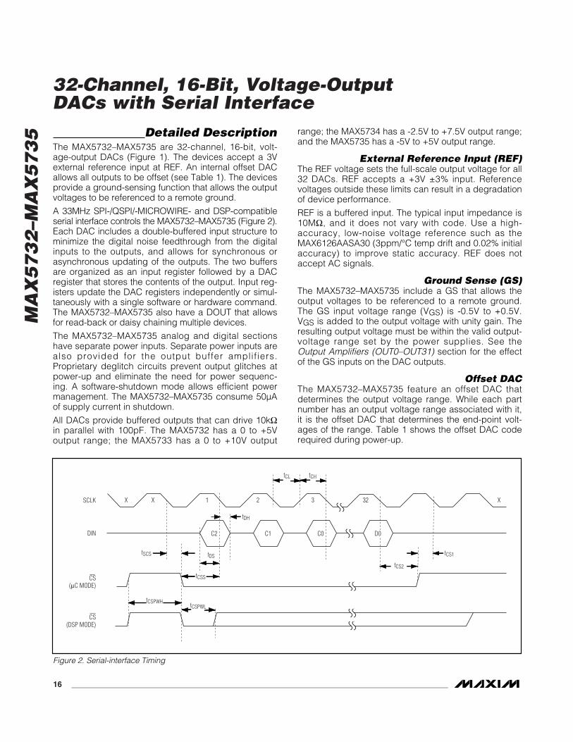
Detailed DescriptionThe MAX5732–MAX5735 are 32-channel, 16-bit, volt-age-output DACs (Figure 1). The devices accept a 3Vexternal reference input at REF. An internal offset DACallows all outputs to be offset (see Table 1). The devicesprovide a ground-sensing function that allows the outputvoltages to be referenced to a remote ground.
A 33MHz SPI-/QSPI/-MICROWIRE- and DSP-compatibleserial interface controls the MAX5732–MAX5735 (Figure 2).Each DAC includes a double-buffered input structure tominimize the digital noise feedthrough from the digitalinputs to the outputs, and allows for synchronous orasynchronous updating of the outputs. The two buffersare organized as an input register followed by a DACregister that stores the contents of the output. Input reg-isters update the DAC registers independently or simul-taneously with a single software or hardware command.The MAX5732–MAX5735 also have a DOUT that allowsfor read-back or daisy chaining multiple devices.
The MAX5732–MAX5735 analog and digital sectionshave separate power inputs. Separate power inputs arealso provided for the output buffer amplif iers.Proprietary deglitch circuits prevent output glitches atpower-up and eliminate the need for power sequenc-ing. A software-shutdown mode allows efficient powermanagement. The MAX5732–MAX5735 consume 50µAof supply current in shutdown.
All DACs provide buffered outputs that can drive 10kΩin parallel with 100pF. The MAX5732 has a 0 to +5Voutput range; the MAX5733 has a 0 to +10V output
range; the MAX5734 has a -2.5V to +7.5V output range;and the MAX5735 has a -5V to +5V output range.
External Reference Input (REF)The REF voltage sets the full-scale output voltage for all32 DACs. REF accepts a +3V ±3% input. Referencevoltages outside these limits can result in a degradationof device performance.
REF is a buffered input. The typical input impedance is10MΩ, and it does not vary with code. Use a high-accuracy, low-noise voltage reference such as theMAX6126AASA30 (3ppm/°C temp drift and 0.02% initialaccuracy) to improve static accuracy. REF does notaccept AC signals.
Ground Sense (GS)The MAX5732–MAX5735 include a GS that allows theoutput voltages to be referenced to a remote ground.The GS input voltage range (VGS) is -0.5V to +0.5V.VGS is added to the output voltage with unity gain. Theresulting output voltage must be within the valid output-voltage range set by the power supplies. See theOutput Amplifiers (OUT0–OUT31) section for the effectof the GS inputs on the DAC outputs.
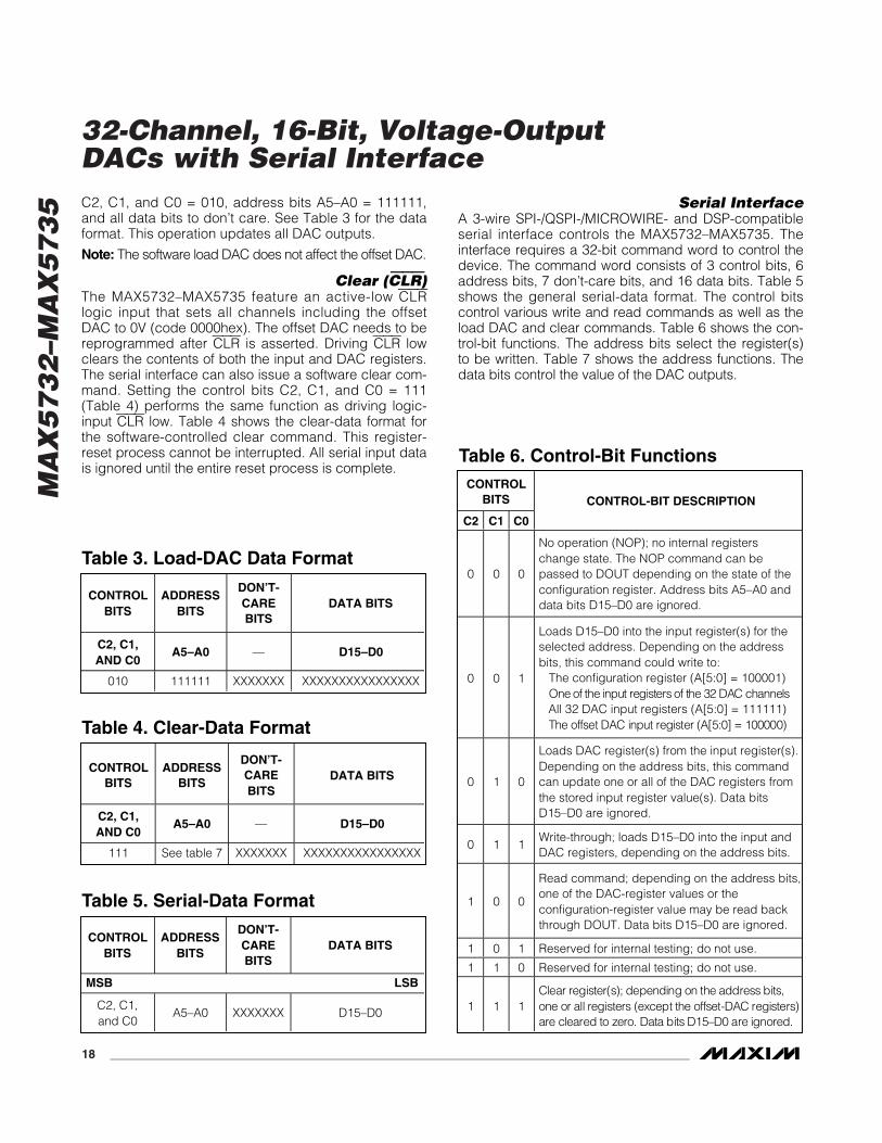
Offset DACThe MAX5732–MAX5735 feature an offset DAC thatdetermines the output voltage range. While each partnumber has an output voltage range associated with it,it is the offset DAC that determines the end-point volt-ages of the range. Table 1 shows the offset DAC coderequired during power-up.
SCLK X X 1 2 3 32 X
DIN D0C0C1C2
tCL tCH
tDH
tDS
tCS2
tCS1
tCSS
tSCS
tCSPWLtCSPWH
CS(DSP MODE)
CS(µC MODE)
Figure 2. Serial-interface Timing
MA
X5
73
2–M
AX
57
35
32-Channel, 16-Bit, Voltage-Output DACs with Serial Interface
______________________________________________________________________________________ 17
Note: The offset DAC of every device can be pro-grammed with any of the four output voltage ranges.However, the specif ications in the ElectricalCharacteristics table are only guaranteed (productiontested) for the offset code associated with each partic-ular part number. For example, the MAX5734 specifica-tions are only valid with the MAX5734 offset- DAC codeshown in Table 1.
The offset DAC is summed with GS (Figure 1). The offsetDAC can also cancel the offset of the output buffers.Any change in the offset DAC affects all 32 DACs.
The offset DAC is also configured identically to theother 32 DACs with an input and DAC register. Write tothe offset DAC through the serial interface by usingcontrol bits C2, C1, and C0 = 001 followed by the databits D15–D0. The CLR command affects the offset DACas well as the other DACs.
The data format for the offset DAC codes are: control bitsC2, C1, and C0 = 011, address bits A5–A0 = 100000, 7don’t-care bits, and 16 data bits as shown in Table 2.
Output Amplifiers (OUT0–OUT31)All DAC outputs are internally buffered. The internalbuffers provide gain, improved load regulation, and tran-sition glitch suppression for the DAC outputs. The outputbuffers slew at 1V/µs and can drive 10kΩ in parallel with100pF. The output buffers are powered by AVCC andVSS. AVCC and VSS determine the maximum outputvoltage range of the device.
The input code, the voltage reference, the offset DACoutput, the voltage on GS, and the gain of the outputamplifier determine the output voltage. Calculate VOUTas follows:
where GAIN = 5/3 for the MAX5732, or GAIN = 10/3 forthe MAX5733/MAX5734/MAX5735.
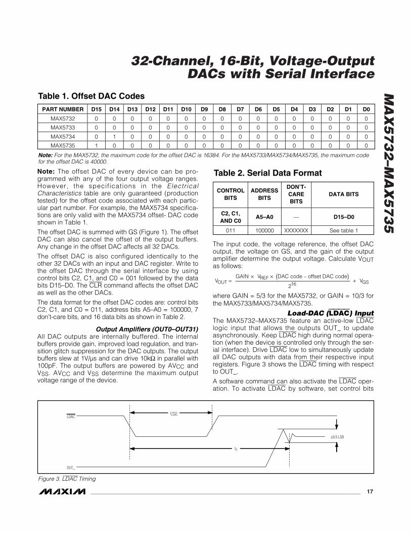
Load-DAC (LDAC) InputThe MAX5732–MAX5735 feature an active-low LDAClogic input that allows the outputs OUT_ to updateasynchronously. Keep LDAC high during normal opera-tion (when the device is controlled only through the ser-ial interface). Drive LDAC low to simultaneously updateall DAC outputs with data from their respective inputregisters. Figure 3 shows the LDAC timing with respectto OUT_.
A software command can also activate the LDAC oper-ation. To activate LDAC by software, set control bits
VGAIN V DAC code offset DAC code
VOUTREF
GS=× × ( )
+−
216
PART NUMBER D15 D14 D13 D12 D11 D10 D9 D8 D7 D6 D5 D4 D3 D2 D1 D0
MAX5732 0 0 0 0 0 0 0 0 0 0 0 0 0 0 0 0
MAX5733 0 0 0 0 0 0 0 0 0 0 0 0 0 0 0 0
MAX5734 0 1 0 0 0 0 0 0 0 0 0 0 0 0 0 0
MAX5735 1 0 0 0 0 0 0 0 0 0 0 0 0 0 0 0
Table 1. Offset DAC Codes
OUT_
±0.5 LSB
tS
tLDACLDAC
Figure 3. LDAC Timing
Note: For the MAX5732, the maximum code for the offset DAC is 16384. For the MAX5733/MAX5734/MAX5735, the maximum codefor the offset DAC is 40000.
Table 2. Serial Data Format
CONTROLBITS
ADDRESSBITS
DON’T-CAREBITS
DATA BITS
C2, C1,AND C0
A5–A0 — D15–D0
011 100000 XXXXXXX See table 1
MA
X5
73
2–M
AX
57
35
32-Channel, 16-Bit, Voltage-Output DACs with Serial Interface
18 ______________________________________________________________________________________
C2, C1, and C0 = 010, address bits A5–A0 = 111111,and all data bits to don’t care. See Table 3 for the dataformat. This operation updates all DAC outputs.
Note: The software load DAC does not affect the offset DAC.
Clear (CLR)The MAX5732–MAX5735 feature an active-low CLRlogic input that sets all channels including the offsetDAC to 0V (code 0000hex). The offset DAC needs to bereprogrammed after CLR is asserted. Driving CLR lowclears the contents of both the input and DAC registers.The serial interface can also issue a software clear com-mand. Setting the control bits C2, C1, and C0 = 111(Table 4) performs the same function as driving logic-input CLR low. Table 4 shows the clear-data format forthe software-controlled clear command. This register-reset process cannot be interrupted. All serial input datais ignored until the entire reset process is complete.
Serial InterfaceA 3-wire SPI-/QSPI-/MICROWIRE- and DSP-compatibleserial interface controls the MAX5732–MAX5735. Theinterface requires a 32-bit command word to control thedevice. The command word consists of 3 control bits, 6address bits, 7 don’t-care bits, and 16 data bits. Table 5shows the general serial-data format. The control bitscontrol various write and read commands as well as theload DAC and clear commands. Table 6 shows the con-trol-bit functions. The address bits select the register(s)to be written. Table 7 shows the address functions. Thedata bits control the value of the DAC outputs.
Table 3. Load-DAC Data Format
CONTROLBITS
ADDRESSBITS
DON’T-CAREBITS
DATA BITS
C2, C1,AND C0
A5–A0 — D15–D0
010 111111 XXXXXXX XXXXXXXXXXXXXXXX
Table 4. Clear-Data Format
CONTROLBITS
ADDRESSBITS
DON’T-CAREBITS
DATA BITS
C2, C1,AND C0
A5–A0 — D15–D0
111 See table 7 XXXXXXX XXXXXXXXXXXXXXXX
Table 5. Serial-Data Format
CONTROLBITS
ADDRESSBITS
DON’T-CAREBITS
DATA BITS
MSB LSB
C2, C1,and C0
A5–A0 XXXXXXX D15–D0
Table 6. Control-Bit FunctionsCONTROL
BITS
C2 C1 C0
CONTROL-BIT DESCRIPTION
0 0 0
No operation (NOP); no internal registerschange state. The NOP command can bepassed to DOUT depending on the state of theconfiguration register. Address bits A5–A0 anddata bits D15–D0 are ignored.
0 0 1
Loads D15–D0 into the input register(s) for theselected address. Depending on the addressbits, this command could write to: The configuration register (A[5:0] = 100001) One of the i np ut r eg i ster s of the 32 D AC channel s All 32 DAC input registers (A[5:0] = 111111) The offset D AC i np ut r eg i ster ( A[ 5:0] = 100000)
0 1 0
Loads DAC register(s) from the input register(s).Depending on the address bits, this commandcan update one or all of the DAC registers fromthe stored input register value(s). Data bitsD15–D0 are ignored.
0 1 1Write-through; loads D15–D0 into the input andDAC registers, depending on the address bits.
1 0 0
Read command; depending on the address bits,one of the DAC-register values or theconfiguration-register value may be read backthrough DOUT. Data bits D15–D0 are ignored.
1 0 1 Reserved for internal testing; do not use.
1 1 0 Reserved for internal testing; do not use.
1 1 1C l ear r eg i ster ( s) ; d ep end i ng on the ad d r ess b i ts,one or al l r eg i ster s ( excep t the offset- D AC r eg i ster s) ar e cl ear ed to zer o. D ata b i ts D 15–D 0 ar e i g nor ed .
MA
X5
73
2–M
AX
57
35
32-Channel, 16-Bit, Voltage-Output DACs with Serial Interface
______________________________________________________________________________________ 19
Table 7. Address-Bit Functions
ADDRESS BITS
A5 A4 A3 A2 A1 A0CONTROL FUNCTION
0 0 0 0 0 0 DAC0
0 0 0 0 0 1 DAC1
0 0 0 0 1 0 DAC2
0 0 0 0 1 1 DAC3
0 0 0 1 0 0 DAC4
0 0 0 1 0 1 DAC5
0 0 0 1 1 0 DAC6
0 0 0 1 1 1 DAC7
0 0 1 0 0 0 DAC8
0 0 1 0 0 1 DAC9
0 0 1 0 1 0 DAC10
0 0 1 0 1 1 DAC11
0 0 1 1 0 0 DAC12
0 0 1 1 0 1 DAC13
0 0 1 1 1 0 DAC14
0 0 1 1 1 1 DAC15
0 1 0 0 0 0 DAC16
0 1 0 0 0 1 DAC17
0 1 0 0 1 0 DAC18
0 1 0 0 1 1 DAC19
0 1 0 1 0 0 DAC20
0 1 0 1 0 1 DAC21
0 1 0 1 1 0 DAC22
0 1 0 1 1 1 DAC23
0 1 1 0 0 0 DAC24
0 1 1 0 0 1 DAC25
0 1 1 0 1 0 DAC26
0 1 1 0 1 1 DAC27
0 1 1 1 0 0 DAC28
0 1 1 1 0 1 DAC29
0 1 1 1 1 0 DAC30
0 1 1 1 1 1 DAC31
1 0 0 0 0 0 Offset DAC
1 0 0 0 0 1
C onfi g ur ati on r eg i ster ; contr ol b i ts C 2, C 1, and C 0 = 010 and C 2, C 1, and C 0 = 011 set the er r or fl ag i n the confi g ur ati on r eg i ster .D o not use these contr ol b i ts w i ththese ad d r ess b i ts.
ADDRESS BITS
A5 A4 A3 A2 A1 A0CONTROL FUNCTION
1 0 0 0 1 0 C om m and r eser ved ; d o not use.
1 0 0 0 1 1 C om m and r eser ved ; d o not use.
1 0 0 1 0 0 C om m and r eser ved ; d o not use.
1 0 0 1 0 1 C om m and r eser ved ; d o not use.
1 0 0 1 1 0 C om m and r eser ved ; d o not use.
1 0 0 1 1 1 C om m and r eser ved ; d o not use.
1 0 1 0 0 0 C om m and r eser ved ; d o not use.
1 0 1 0 0 1 C om m and r eser ved ; d o not use.
1 0 1 0 1 0 C om m and r eser ved ; d o not use.
1 0 1 0 1 1 C om m and r eser ved ; d o not use.
1 0 1 1 0 0 C om m and r eser ved ; d o not use.
1 0 1 1 0 1 C om m and r eser ved ; d o not use.
1 0 1 1 1 0 C om m and r eser ved ; d o not use.
1 0 1 1 1 1 C om m and r eser ved ; d o not use.
1 1 0 0 0 0 C om m and r eser ved ; d o not use.
1 1 0 0 0 1 C om m and r eser ved ; d o not use.
1 1 0 0 1 0 C om m and r eser ved ; d o not use.
1 1 0 0 1 1 C om m and r eser ved ; d o not use.
1 1 0 1 0 0 C om m and r eser ved ; d o not use.
1 1 0 1 0 1 C om m and r eser ved ; d o not use.
1 1 0 1 1 0 C om m and r eser ved ; d o not use.
1 1 0 1 1 1 C om m and r eser ved ; d o not use.
1 1 1 0 0 0 C om m and r eser ved ; d o not use.
1 1 1 0 0 1 C om m and r eser ved ; d o not use.
1 1 1 0 1 0 C om m and r eser ved ; d o not use.
1 1 1 0 1 1 C om m and r eser ved ; d o not use.
1 1 1 1 0 0 C om m and r eser ved ; d o not use.
1 1 1 1 0 1 C om m and r eser ved ; d o not use.
1 1 1 1 1 0 C om m and r eser ved ; d o not use.
1 1 1 1 1 1
All channels (DAC31–DAC0);used for write commands only.Read commands cannot beused with these address bits.
MA
X5
73
2–M
AX
57
35
32-Channel, 16-Bit, Voltage-Output DACs with Serial Interface
20 ______________________________________________________________________________________
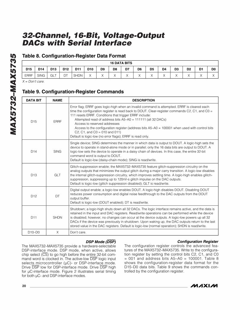
DSP Mode (DSP)The MAX5732–MAX5735 provide a hardware-selectableDSP-interface mode. DSP mode, when active, allowschip select (CS) to go high before the entire 32-bit com-mand word is clocked in. The active-low DSP logic inputselects microcontroller (µC)- or DSP-interface mode.Drive DSP low for DSP-interface mode. Drive DSP highfor µC-interface mode. Figure 2 illustrates serial timingfor both µC- and DSP-interface modes.
Configuration RegisterThe configuration register controls the advanced fea-tures of the MAX5732–MAX5735. Write to the configura-tion register by setting the control bits C2, C1, and C0= 001 and address bits A5–A0 = 100001. Table 8shows the configuration-register data format for theD15–D0 data bits. Table 9 shows the commands con-trolled by the configuration register.
Table 9. Configuration-Register Commands
DATA BIT NAME DESCRIPTION
D15 ERRF
Error flag; ERRF goes logic-high when an invalid command is attempted. ERRF is cleared eachtime the configuration register is read back to DOUT. Clear-register commands C2, C1, and C0 =111 resets ERRF. Conditions that trigger ERRF include: Attempted read of address bits A5–A0 = 111111 (all 32 DACs) Access to reserved addresses Access to the configuration register (address bits A5–A0 = 100001 when used with control bits C2, C1, and C0 = 010 and 011)Default is logic-low (no error flags); ERRF is read only.
D14 SING
Single device; SING determines the manner in which data is output to DOUT. A logic-high sets thedevice to operate in stand-alone mode or in parallel; only the 16 data bits are output to DOUT. Alogic-low sets the device to operate in a daisy chain of devices. In this case, the entire 32-bitcommand word is output to DOUT.Default is logic-low (daisy-chain mode); SING is read/write.
D13 GLT
Glitch-suppression enable; the MAX5732–MAX5735 feature glitch-suppression circuitry on theanalog outputs that minimizes the output glitch during a major carry transition. A logic-low disablesthe internal glitch-suppression circuitry, which improves settling time. A logic-high enables glitch-suppression, suppressing up to 120nV-s glitch impulse on the DAC outputs.Default is logic-low (glitch suppression disabled); GLT is read/write.
D12 DT
Digital output enable; a logic-low enables DOUT. A logic-high disables DOUT. Disabling DOUTreduces power consumption and digital noise feedthrough to the DAC outputs from the DOUToutput buffer.Default is logic-low (DOUT enabled); DT is read/write.
D11 SHDN
Shutdown; a logic-high shuts down all 32 DACs. The logic interface remains active, and the data isretained in the input and DAC registers. Read/write operations can be performed while the deviceis disabled; however, no changes can occur at the device outputs. A logic-low powers up all 32DACs if the device was previously in shutdown. Upon waking up, the DAC outputs return to the laststored value in the DAC registers. Default is logic-low (normal operation); SHDN is read/write.
D10–D0 X Don’t care.
Table 8. Configuration-Register Data Format16 DATA BITS
D15 D14 D13 D12 D11 D10 D9 D8 D7 D6 D5 D4 D3 D2 D1 D0
ERRF SING GLT DT SHDN X X X X X X X X X X X
X = Don’t care.
MA
X5
73
2–M
AX
57
35
32-Channel, 16-Bit, Voltage-Output DACs with Serial Interface
______________________________________________________________________________________ 21
SINGWhen SING = 0 (default power-up mode), the device isin daisy-chain mode. DOUT follows DIN after 32 clockcycles. For the read command, DOUT provides theread data in the next cycle following CS rising edge.The 16 data bits of the previous command word areclocked out on the last 16 clock cycles of the currentcommand word.
When SING = 1, the device is in stand-alone mode. Toreduce the time it takes to read data out, the read data isprovided at DOUT as the 16 data bits of the current com-mand are clocked in. The device acts on an incomingcommand word independent of the rising edge of CS.
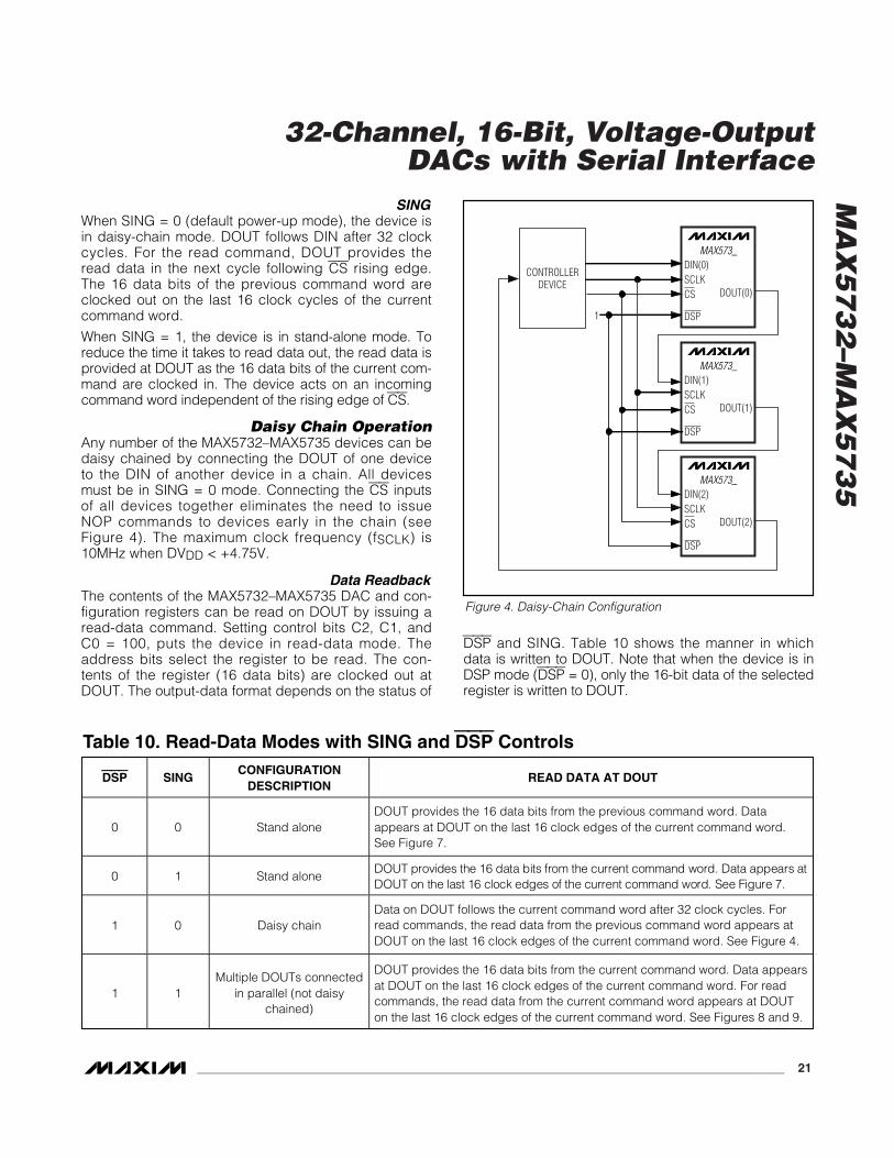
Daisy Chain OperationAny number of the MAX5732–MAX5735 devices can bedaisy chained by connecting the DOUT of one deviceto the DIN of another device in a chain. All devicesmust be in SING = 0 mode. Connecting the CS inputsof all devices together eliminates the need to issueNOP commands to devices early in the chain (seeFigure 4). The maximum clock frequency (fSCLK) is10MHz when DVDD < +4.75V.
Data ReadbackThe contents of the MAX5732–MAX5735 DAC and con-figuration registers can be read on DOUT by issuing aread-data command. Setting control bits C2, C1, andC0 = 100, puts the device in read-data mode. Theaddress bits select the register to be read. The con-tents of the register (16 data bits) are clocked out atDOUT. The output-data format depends on the status of
DSP and SING. Table 10 shows the manner in whichdata is written to DOUT. Note that when the device is inDSP mode (DSP = 0), only the 16-bit data of the selectedregister is written to DOUT.
Table 10. Read-Data Modes with SING and DSP Controls
DSP SINGCONFIGURATION
DESCRIPTIONREAD DATA AT DOUT
0 0 Stand aloneDOUT provides the 16 data bits from the previous command word. Dataappears at DOUT on the last 16 clock edges of the current command word.See Figure 7.
0 1 Stand aloneD OU T p r ovi d es the 16 d ata b i ts fr om the cur r ent com m and w or d . D ata ap p ear s atD OU T on the l ast 16 cl ock ed g es of the cur r ent com m and w or d . S ee Fi g ur e 7.
1 0 Daisy chainData on DOUT follows the current command word after 32 clock cycles. Forread commands, the read data from the previous command word appears atDOUT on the last 16 clock edges of the current command word. See Figure 4.
1 1Multiple DOUTs connected
in parallel (not daisychained)
DOUT provides the 16 data bits from the current command word. Data appearsat DOUT on the last 16 clock edges of the current command word. For readcommands, the read data from the current command word appears at DOUTon the last 16 clock edges of the current command word. See Figures 8 and 9.
CONTROLLERDEVICE
DIN(0)
DOUT(0)
1
SCLKCS
DSP
MAX573_
DIN(1)
DOUT(1)SCLKCS
DSP
MAX573_
DIN(2)
DOUT(2)SCLKCS
DSP
MAX573_
Figure 4. Daisy-Chain Configuration
MA
X5
73
2–M
AX
57
35
32-Channel, 16-Bit, Voltage-Output DACs with Serial Interface
22 ______________________________________________________________________________________
W WD2 W WD1 W WD0 R XX R XX R XX X XX X XX X XXDIN(0)
CS
DOUT(0) WD1WWD2W XXRXXRWD0W R RD0 X XX X XX
DOUT(1) W WD2 W WD1 W WD0 R XX R RD1 R RD0 X XX
DOUT(2) W WD2 W WD1 W WD0 R RD2 R RD1 R RD0
W WD2 R XX W WD0 R XX W WD1 R XX X XX X XX X XXDIN(0)
CS
DOUT(0) XXRWD2W WD1WXXRWD0W R RD0 X XX X XX
DOUT(1) W WD2 R RD1 W WD0 R XX W WD1 R RD0 X XX
DOUT(2) W WD2 R RD1 W WD0 R RD2 W WD1 R RD0
Figure 5. Example 1 of a Daisy-Chain Data Sequence
W/WD0 = 32-bit word with a write command; WD0 writes data for device 0. The 0 refers to the position in the daisy chain (0 is closestto the bus master). Devices 1 and 2 are devices further down the chain.R/RD2 = 32-bit word with a read command; RD2 reads data from device 2.X = Don’t care (for X in the data or command position).
Figure 6. Example 2 of a Daisy-Chain Data Sequence
W/WD0 = 32-bit word with a write command; WD0 writes data for device 0. The 0 refers to the position in the daisy chain (0 is closestto the bus master). Devices 1 and 2 are devices further down the chain.R/RD2 = 32-bit word with a read command; RD2 reads data from device 2.X = Don’t care (for X in the data or command position).
MA
X5
73
2–M
AX
57
35
32-Channel, 16-Bit, Voltage-Output DACs with Serial Interface
______________________________________________________________________________________ 23
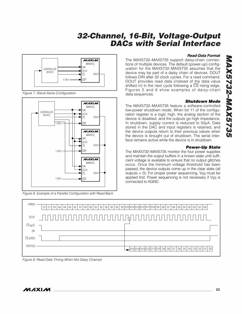
Read-Data FormatThe MAX5732–MAX5735 support daisy-chain connec-tions of multiple devices. The default (power-up) config-uration for the MAX5732–MAX5735 assumes that thedevice may be part of a daisy chain of devices. DOUTfollows DIN after 32 clock cycles. For a read command,DOUT provides read data (instead of the data valueshifted in) in the next cycle following a CS rising edge.Figures 5 and 6 show examples of daisy-chain data sequences.
Shutdown ModeThe MAX5732–MAX5735 feature a software-controlledlow-power shutdown mode. When bit 11 of the configu-ration register is a logic high, the analog section of thedevice is disabled, and the outputs go high impedance.In shutdown, supply current is reduced to 50µA. Datastored in the DAC and input registers is retained, andthe device outputs return to their previous values whenthe device is brought out of shutdown. The serial inter-face remains active while the device is in shutdown.
Power-Up StateThe MAX5732–MAX5735 monitor the four power suppliesand maintain the output buffers in a known state until suffi-cient voltage is available to ensure that no output glitchesoccur. Once the minimum voltage threshold has beenpassed, the device outputs come up in the clear state (alloutputs = 0). For proper power sequencing, VSS must beapplied first. Power sequencing is not necessary if VSS isconnected to AGND.
CONTROLLERDEVICE
DIN
DOUT
1 OR 0
SCLKCS
MAX573_
DSP
Figure 7. Stand-Alone Configuration
CONTROLLERDEVICE
DIN
DOUT
1 OR 0
1 OR 0
1 OR 0
SCLKCS
MAX573_
DIN
DOUTSCLKCS
MAX573_
DIN
DOUTSCLKCS
MAX573_
DSP
DSP
DSP
Figure 8. Example of a Parallel Configuration with Read-Back
C1C2 C0 A5 A4 A3 A2 A1 A0 Sp Sp Sp Sp Sp Sp Sp D15 D14 D13 D12 D11 D10 D9 D8 D7 D6 D5 D4 D3 D2 D1 D0
D15 D14 D13 D12 D11 D10 D9 D8 D7 D6 D5 D4 D3 D2 D1 D0
DIN(0)
SCLK
CS (µC)
CS (DSP)
DOUT(0)
OR
Figure 9. Read Data Timing When Not Daisy Chained
MA
X5
73
2–M
AX
57
35
32-Channel, 16-Bit, Voltage-Output DACs with Serial Interface
24 ______________________________________________________________________________________
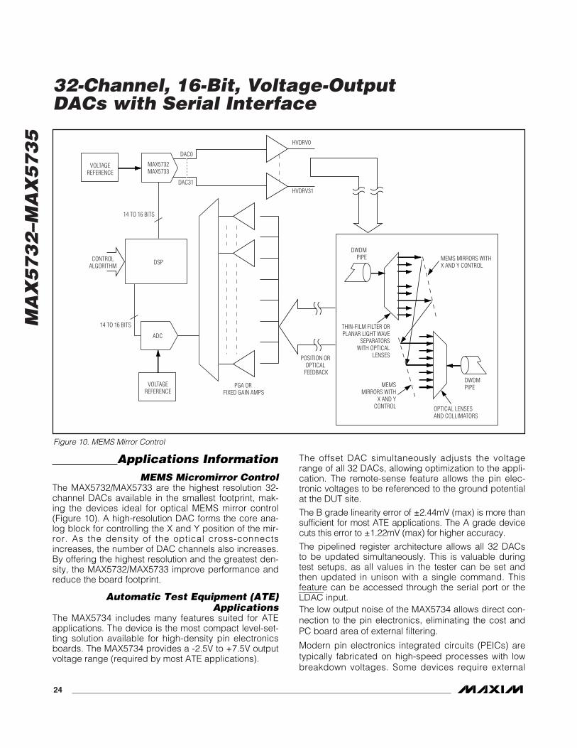
Applications InformationMEMS Micromirror Control
The MAX5732/MAX5733 are the highest resolution 32-channel DACs available in the smallest footprint, mak-ing the devices ideal for optical MEMS mirror control(Figure 10). A high-resolution DAC forms the core ana-log block for controlling the X and Y position of the mir-ror. As the density of the optical cross-connectsincreases, the number of DAC channels also increases.By offering the highest resolution and the greatest den-sity, the MAX5732/MAX5733 improve performance andreduce the board footprint.
Automatic Test Equipment (ATE)Applications
The MAX5734 includes many features suited for ATEapplications. The device is the most compact level-set-ting solution available for high-density pin electronicsboards. The MAX5734 provides a -2.5V to +7.5V outputvoltage range (required by most ATE applications).
The offset DAC simultaneously adjusts the voltagerange of all 32 DACs, allowing optimization to the appli-cation. The remote-sense feature allows the pin elec-tronic voltages to be referenced to the ground potentialat the DUT site.
The B grade linearity error of ±2.44mV (max) is more thansufficient for most ATE applications. The A grade devicecuts this error to ±1.22mV (max) for higher accuracy.
The pipelined register architecture allows all 32 DACsto be updated simultaneously. This is valuable duringtest setups, as all values in the tester can be set andthen updated in unison with a single command. Thisfeature can be accessed through the serial port or theLDAC input.The low output noise of the MAX5734 allows direct con-nection to the pin electronics, eliminating the cost andPC board area of external filtering.
Modern pin electronics integrated circuits (PEICs) aretypically fabricated on high-speed processes with lowbreakdown voltages. Some devices require external
ADC
MAX5732MAX5733
DAC0
HVDRV0
HVDRV31DAC31
14 TO 16 BITS
VOLTAGEREFERENCE
VOLTAGEREFERENCE
DSPCONTROLALGORITHM
POSITION OR OPTICAL
FEEDBACK
PGA OR FIXED GAIN AMPS
MEMS MIRRORS WITHX AND Y CONTROL
THIN-FILM FILTER ORPLANAR LIGHT WAVE
SEPARATORSWITH OPTICAL
LENSES
MEMSMIRRORS WITH
X AND YCONTROL
DWDMPIPE
OPTICAL LENSESAND COLLIMATORS
14 TO 16 BITS
DWDMPIPE
Figure 10. MEMS Mirror Control

MA
X5
73
2–M
AX
57
35
32-Channel, 16-Bit, Voltage-Output DACs with Serial Interface
______________________________________________________________________________________ 25
protection on their reference inputs to satisfy absolutemaximum ratings. The MAX5734 features outputs thatare almost rail-to-rail. This allows the AVCC and VSSsupplies to be set to voltages within the absolute maxi-mum ratings of the PEIC. This guarantees that the PEICis protected in all situations.
Additional protection is provided by the MAX5734glitch-free power-up into the clear state with all DACoutputs set to approximately 0V. Either the serial port orthe CLR input can assert the clear function.
Power Supplies, Bypassing,Decoupling, and Layout
Grounding and power-supply decoupling strongly influ-ence device performance. Digital signals can couplethrough the reference input, power supplies, and groundconnection. Proper grounding and layout can reduce
digital feedthrough and crosstalk. Bypass all power sup-plies with an additional 0.1µF and 1µF on each pin, asclose to the device as possible. Refer to the MAX5732–MAX5735 evaluation kit for a suggested layout.
The MAX5732–MAX5735 have four separate powersupplies. AVDD powers the internal analog circuitry(except for the output buffers) and DVDD powers thedigital section of the device. AVCC and VSS power theoutput buffers.
The MAX5732–MAX5735 feature an exposed paddle onthe backside of the package for improved power dissi-pation. The exposed paddle is electrically connected toVSS, and should be soldered to a large copper planethat shares the same potential. For more information onthe exposed paddle QFN package, refer to the followingwebsite: http://pdfserv.maxim-ic.com/arpdf/AppNotes/4hfan081.pdf
5859606162 5455565763
38
39
40
41
42
43
44
45
46
47
VSS
DSP
OUT1
0
TQFP
TOP VIEW
OUT1
1
OUT1
2
OUT1
3
OUT1
4
OUT1
5
AVDD
REFG
ND
AVCC
OUT1
6
5253 495051
OUT1
7
OUT1
8
OUT1
9
OUT2
0
N.C.
N.C.
DOUTCS DI
N
SCLK
DGND
DVDD CLR
LDAC
REFG
NDGS
AVDDRE
F
V SS
OUT21
OUT22
VSS
AGND
OUT23
OUT24
OUT25
OUT26
OUT27
OUT28
33
34
35
36
37 OUT29
OUT30
OUT31
N.C.
N.C.
OUT3
AGND
OUT4
OUT5
OUT6
N.C.
N.C.
OUT0
OUT1
OUT2
N.C.
OUT7
OUT8
OUT9
48 AVCCAVCC
64
N.C.
N.C.
2322212019 2726252418 2928 32313017
11
10
9
8
7
6
5
4
3
2
16
15
14
13
12
1
MAX5732–MAX5735
Pin Configurations (continued) Chip InformationTRANSISTOR COUNT: 152,000
PROCESS: BiCMOS
MA
X5
73
2–M
AX
57
35
32-Channel, 16-Bit, Voltage-Output DACs with Serial Interface
26 ______________________________________________________________________________________
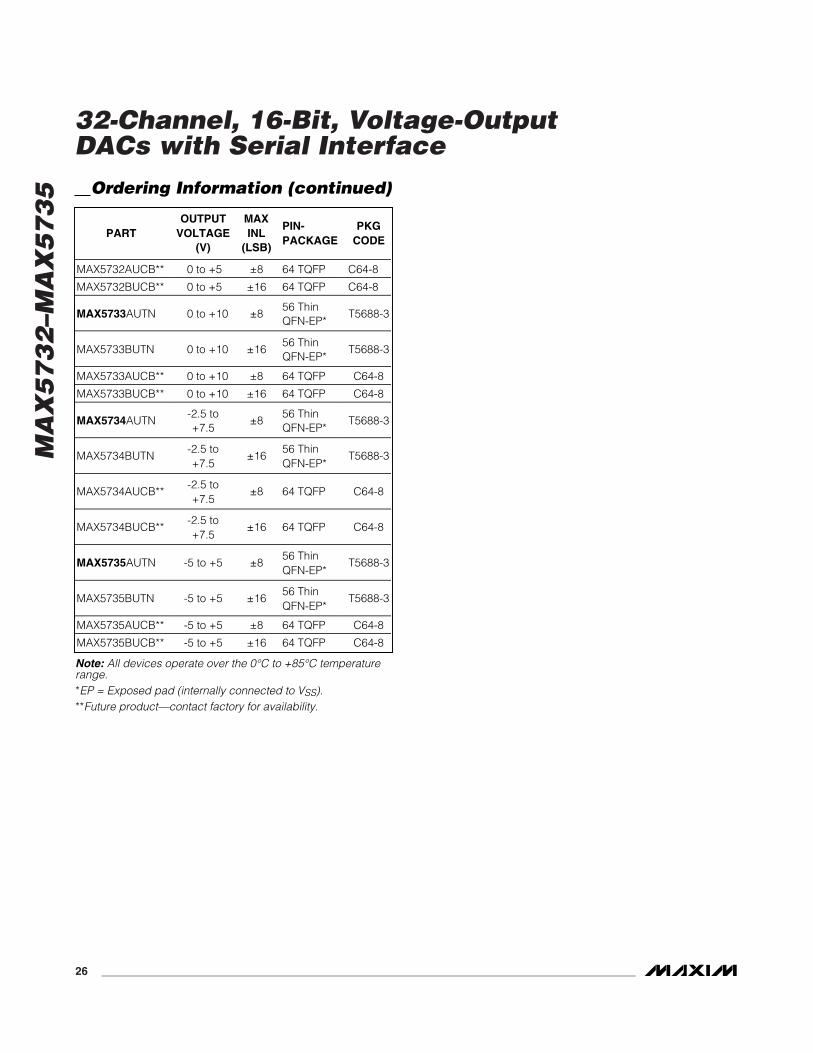
Note: All devices operate over the 0°C to +85°C temperaturerange.*EP = Exposed pad (internally connected to VSS).**Future product—contact factory for availability.
Ordering Information (continued)
PARTOUTPUT
VOLTAGE(V)
MAXINL
(LSB)
PIN-PACKAGE
PKGCODE
MAX5732AUCB** 0 to +5 ±8 64 TQFP C64-8
MAX5732BUCB** 0 to +5 ±16 64 TQFP C64-8
MAX5733AUTN 0 to +10 ±856 ThinQFN-EP*
T5688-3
MAX5733BUTN 0 to +10 ±1656 ThinQFN-EP*
T5688-3
MAX5733AUCB** 0 to +10 ±8 64 TQFP C64-8
MAX5733BUCB** 0 to +10 ±16 64 TQFP C64-8
MAX5734AUTN-2.5 to+7.5
±856 ThinQFN-EP*
T5688-3
MAX5734BUTN-2.5 to+7.5
±1656 ThinQFN-EP*
T5688-3
MAX5734AUCB**-2.5 to+7.5
±8 64 TQFP C64-8
MAX5734BUCB**-2.5 to+7.5
±16 64 TQFP C64-8
MAX5735AUTN -5 to +5 ±856 ThinQFN-EP*
T5688-3
MAX5735BUTN -5 to +5 ±1656 ThinQFN-EP*
T5688-3
MAX5735AUCB** -5 to +5 ±8 64 TQFP C64-8
MAX5735BUCB** -5 to +5 ±16 64 TQFP C64-8
MA
X5
73
2–M
AX
57
35
32-Channel, 16-Bit, Voltage-Output DACs with Serial Interface
______________________________________________________________________________________ 27
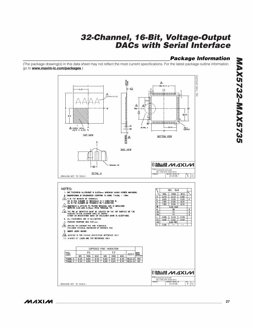
Package Information(The package drawing(s) in this data sheet may not reflect the most current specifications. For the latest package outline information,go to www.maxim-ic.com/packages.)
56L
THIN
QFN
.EP
S
PACKAGE OUTLINE
21-0135 21
E
56L THIN QFN, 8x8x0.8mm
PACKAGE OUTLINE
21-0135 22
E
56L THIN QFN, 8x8x0.8mm

MA
X5
73
2–M
AX
57
35
32-Channel, 16-Bit, Voltage-Output DACs with Serial Interface
Maxim cannot assume responsibility for use of any circuitry other than circuitry entirely embodied in a Maxim product. No circuit patent licenses areimplied. Maxim reserves the right to change the circuitry and specifications without notice at any time.
28 ____________________Maxim Integrated Products, 120 San Gabriel Drive, Sunnyvale, CA 94086 408-737-7600
© 2005 Maxim Integrated Products Printed USA is a registered trademark of Maxim Integrated Products, Inc.
Package Information (continued)(The package drawing(s) in this data sheet may not reflect the most current specifications. For the latest package outline information,go to www.maxim-ic.com/packages.)
64L,
10x
10x1
.4 T
QFP
.EP
S