Embed Size (px)
Citation preview
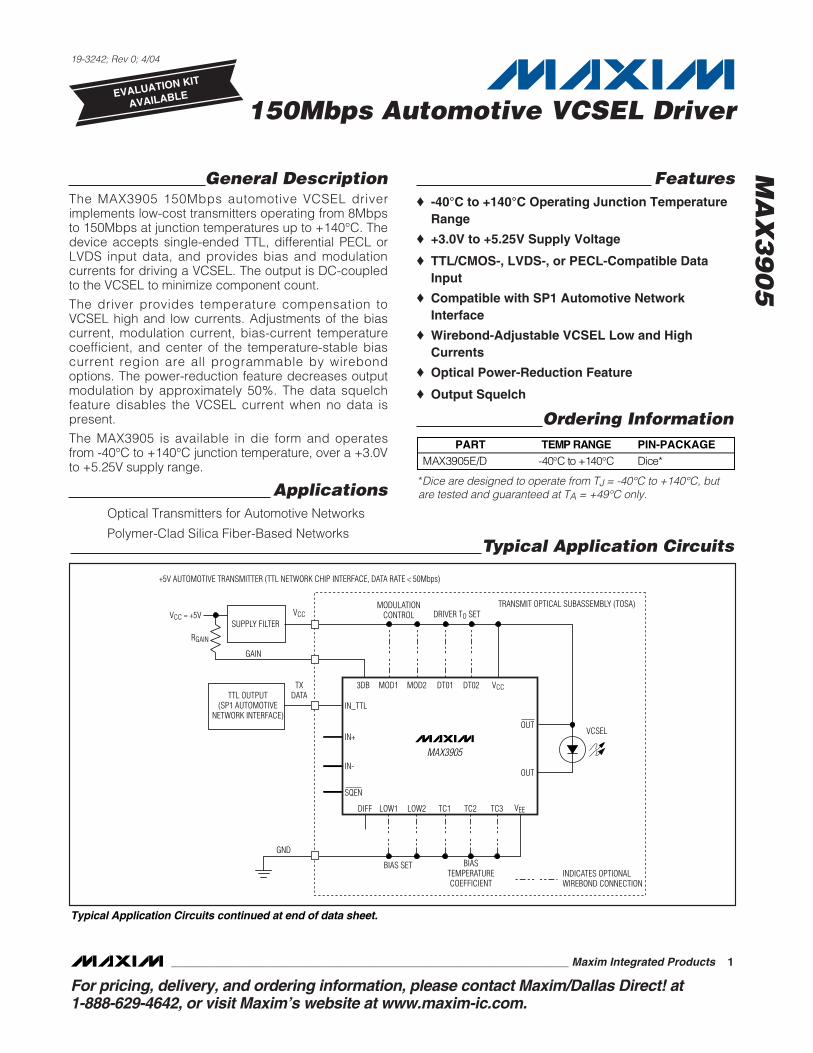
General DescriptionThe MAX3905 150Mbps automotive VCSEL driverimplements low-cost transmitters operating from 8Mbpsto 150Mbps at junction temperatures up to +140°C. Thedevice accepts single-ended TTL, differential PECL orLVDS input data, and provides bias and modulationcurrents for driving a VCSEL. The output is DC-coupledto the VCSEL to minimize component count.
The driver provides temperature compensation toVCSEL high and low currents. Adjustments of the biascurrent, modulation current, bias-current temperaturecoefficient, and center of the temperature-stable biascurrent region are all programmable by wirebondoptions. The power-reduction feature decreases outputmodulation by approximately 50%. The data squelchfeature disables the VCSEL current when no data ispresent.
The MAX3905 is available in die form and operatesfrom -40°C to +140°C junction temperature, over a +3.0Vto +5.25V supply range.
ApplicationsOptical Transmitters for Automotive Networks
Polymer-Clad Silica Fiber-Based Networks
Features♦ -40°C to +140°C Operating Junction Temperature
Range
♦ +3.0V to +5.25V Supply Voltage
♦ TTL/CMOS-, LVDS-, or PECL-Compatible DataInput
♦ Compatible with SP1 Automotive NetworkInterface
♦ Wirebond-Adjustable VCSEL Low and HighCurrents
♦ Optical Power-Reduction Feature
♦ Output Squelch
MA
X3
90
5
150Mbps Automotive VCSEL Driver
________________________________________________________________ Maxim Integrated Products 1
MAX3905
GND
TTL OUTPUT(SP1 AUTOMOTIVE
NETWORK INTERFACE)
GAIN
VCC = +5VSUPPLY FILTER
RGAIN
TXDATA
VCC
IN_TTL
IN+
DIFF
3DB
OUT
MOD2MOD1 DT02DT01 VCC
VCSEL
IN-
LOW1 LOW2 TC1 TC2 TC3
BIAS SET BIASTEMPERATURECOEFFICIENT
VEE
MODULATIONCONTROL DRIVER TO SET
INDICATES OPTIONALWIREBOND CONNECTION
SQEN
TRANSMIT OPTICAL SUBASSEMBLY (TOSA)
+5V AUTOMOTIVE TRANSMITTER (TTL NETWORK CHIP INTERFACE, DATA RATE < 50Mbps)
OUT
Ordering Information
Typical Application Circuits
19-3242; Rev 0; 4/04
For pricing, delivery, and ordering information, please contact Maxim/Dallas Direct! at 1-888-629-4642, or visit Maxim’s website at www.maxim-ic.com.
*Dice are designed to operate from TJ = -40°C to +140°C, butare tested and guaranteed at TA = +49°C only.
EVALUATION KIT
AVAILABLE
PART T EM P R AN G E PIN-PACKAGEM AX 3905E /D - 40°C to + 140°C D i ce*
Typical Application Circuits continued at end of data sheet.
MA
X3
90
5
150Mbps Automotive VCSEL Driver
2 _______________________________________________________________________________________
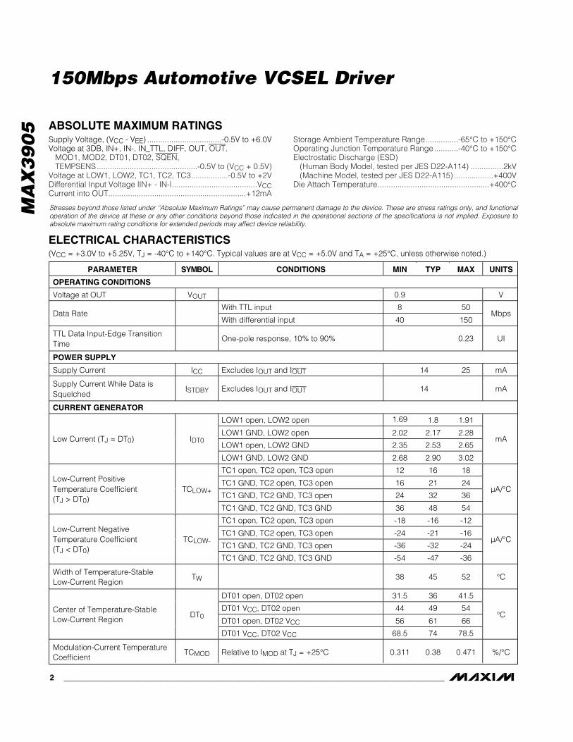
ABSOLUTE MAXIMUM RATINGS
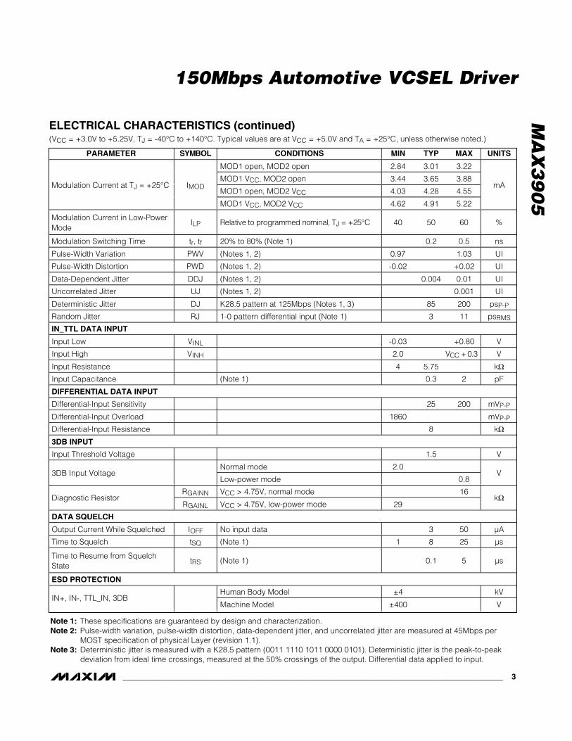
ELECTRICAL CHARACTERISTICS(VCC = +3.0V to +5.25V, TJ = -40°C to +140°C. Typical values are at VCC = +5.0V and TA = +25°C, unless otherwise noted.)
Stresses beyond those listed under “Absolute Maximum Ratings” may cause permanent damage to the device. These are stress ratings only, and functionaloperation of the device at these or any other conditions beyond those indicated in the operational sections of the specifications is not implied. Exposure toabsolute maximum rating conditions for extended periods may affect device reliability.
Supply Voltage, (VCC - VEE) ..................................-0.5V to +6.0VVoltage at 3DB, IN+, IN-, IN_TTL, DIFF, OUT, OUT,
MOD1, MOD2, DT01, DT02, SQEN,TEMPSENS..............................................-0.5V to (VCC + 0.5V)
Voltage at LOW1, LOW2, TC1, TC2, TC3.................-0.5V to +2VDifferential Input Voltage |IN+ - IN-|.......................................VCCCurrent into OUT...............................................................+12mA
Storage Ambient Temperature Range...............-65°C to +150°COperating Junction Temperature Range...........-40°C to +150°CElectrostatic Discharge (ESD)
(Human Body Model, tested per JES D22-A114) ...............2kV(Machine Model, tested per JES D22-A115) ..................+400V
Die Attach Temperature...................................................+400°C
PARAMETER SYM B O L CONDITIONS MIN TYP MAX UNITS
OPERATING CONDITIONS
Voltage at OUT VOUT 0.9 V
With TTL input 8 50Data Rate
With differential input 40 150Mbps
TTL Data Input-Edge TransitionTime
One-pole response, 10% to 90% 0.23 UI
POWER SUPPLY
Supply Current ICC Excludes IOUT and IOUT 14 25 mA
Supply Current While Data isSquelched
ISTDBY Excludes IOUT and IOUT 14 mA
CURRENT GENERATOR
LOW1 open, LOW2 open 1.69 1.8 1.91
LOW1 GND, LOW2 open 2.02 2.17 2.28
LOW1 open, LOW2 GND 2.35 2.53 2.65Low Current (TJ = DT0) IDT0
LOW1 GND, LOW2 GND 2.68 2.90 3.02
mA
TC1 open, TC2 open, TC3 open 12 16 18
TC1 GND, TC2 open, TC3 open 16 21 24
TC1 GND, TC2 GND, TC3 open 24 32 36
Low-Current PositiveTemperature Coefficient(TJ > DT0)
TCLOW+
TC1 GND, TC2 GND, TC3 GND 36 48 54
µA/°C
TC1 open, TC2 open, TC3 open -18 -16 -12
TC1 GND, TC2 open, TC3 open -24 -21 -16
TC1 GND, TC2 GND, TC3 open -36 -32 -24
Low-Current NegativeTemperature Coefficient(TJ < DT0)
TCLOW-
TC1 GND, TC2 GND, TC3 GND -54 -47 -36
µA/°C
Width of Temperature-StableLow-Current Region
TW 38 45 52 °C
DT01 open, DT02 open 31.5 36 41.5
DT01 VCC, DT02 open 44 49 54
DT01 open, DT02 VCC 56 61 66Center of Temperature-StableLow-Current Region
DT0
DT01 VCC, DT02 VCC 68.5 74 78.5
°C
Modulation-Current TemperatureCoefficient
TCMOD Relative to IMOD at TJ = +25°C 0.311 0.38 0.471 %/°C
MA
X3
90
5
150Mbps Automotive VCSEL Driver
_______________________________________________________________________________________ 3
ELECTRICAL CHARACTERISTICS (continued)(VCC = +3.0V to +5.25V, TJ = -40°C to +140°C. Typical values are at VCC = +5.0V and TA = +25°C, unless otherwise noted.)
Note 1: These specifications are guaranteed by design and characterization.Note 2: Pulse-width variation, pulse-width distortion, data-dependent jitter, and uncorrelated jitter are measured at 45Mbps per
MOST specification of physical Layer (revision 1.1).Note 3: Deterministic jitter is measured with a K28.5 pattern (0011 1110 1011 0000 0101). Deterministic jitter is the peak-to-peak
deviation from ideal time crossings, measured at the 50% crossings of the output. Differential data applied to input.
PARAMETER SYM B O L CONDITIONS MIN TYP MAX UNITS
MOD1 open, MOD2 open 2.84 3.01 3.22
MOD1 VCC, MOD2 open 3.44 3.65 3.88
MOD1 open, MOD2 VCC 4.03 4.28 4.55Modulation Current at TJ = +25°C IMOD
MOD1 VCC, MOD2 VCC 4.62 4.91 5.22
mA
Modulation Current in Low-PowerMode
ILP Rel ati ve to p r og r am m ed nom i nal , TJ = + 25° C 40 50 60 %
Modulation Switching Time tr, tf 20% to 80% (Note 1) 0.2 0.5 ns
Pulse-Width Variation PWV (Notes 1, 2) 0.97 1.03 UI
Pulse-Width Distortion PWD (Notes 1, 2) -0.02 +0.02 UI
Data-Dependent Jitter DDJ (Notes 1, 2) 0.004 0.01 UI
Uncorrelated Jitter UJ (Notes 1, 2) 0.001 UI
Deterministic Jitter DJ K28.5 pattern at 125Mbps (Notes 1, 3) 85 200 psP-P
Random Jitter RJ 1-0 pattern differential input (Note 1) 3 11 psRMS
IN_TTL DATA INPUT
Input Low VINL -0.03 +0.80 V
Input High VINH 2.0 V C C + 0.3 V
Input Resistance 4 5.75 kΩInput Capacitance (Note 1) 0.3 2 pF
DIFFERENTIAL DATA INPUT
Differential-Input Sensitivity 25 200 mVP-P
Differential-Input Overload 1860 mVP-P
Differential-Input Resistance 8 kΩ3DB INPUT
Input Threshold Voltage 1.5 V
Normal mode 2.03DB Input Voltage
Low-power mode 0.8V
RGAINN VCC > 4.75V, normal mode 16Diagnostic Resistor
RGAINL VCC > 4.75V, low-power mode 29kΩ
DATA SQUELCH
Output Current While Squelched IOFF No input data 3 50 µA
Time to Squelch tSQ (Note 1) 1 8 25 µs
Time to Resume from SquelchState
tRS (Note 1) 0.1 5 µs
ESD PROTECTION
Human Body Model ±4 kVIN+, IN-, TTL_IN, 3DB
Machine Model ±400 V
MA
X3
90
5
150Mbps Automotive VCSEL Driver
4 _______________________________________________________________________________________
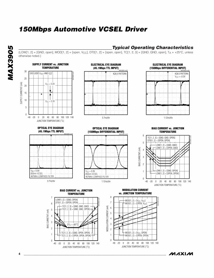
Typical Operating Characteristics(LOW[1, 2] = [GND, open], MOD[1, 2] = [open, VCC], DT0[1, 2] = [open, open], TC[1, 2, 3] = [GND, GND, open], TA = +25°C, unlessotherwise noted.)
0
5
10
15
20
25
30
-40 0-20 20 40 60 80 100 120 140
SUPPLY CURRENT vs. JUNCTIONTEMPERATURE
MAX
3905
toc0
1
JUNCTION TEMPERATURE (°C)
SUPP
LY C
URRE
TNT
(mA)
EXCLUDES IOUT AND IOUT
VCC = 5.0V
VCC = 3.3V
ELECTRICAL EYE DIAGRAM(45.1Mbps TTL INPUT)
MAX3905 toc02
3.7ns/div
K28.5 PATTERN
ELECTRICAL EYE DIAGRAM(150Mbps DIFFERENTIAL INPUT)
1.12ns/div
MAX3905 toc03
K28.5 PATTERNVCC = +3.3V
OPTICAL EYE DIAGRAM (45.1Mbps TTL INPUT)
MAX3905 toc04
3.7ns/div
VIN = 5.0V850nm VCSEL467MHz LOWPASS FILTER
OPTICAL EYE DIAGRAM (150Mbps DIFFERENTIAL INPUT)
MAX3905 toc05
1.12ns/div
VCC = 3.3V850nm VCSEL467MHz LOWPASS FILTER
0
1
2
3
4
5
6
-40 0-20 20 40 60 80 100 120 140
BIAS CURRENT vs. JUNCTIONTEMPERATURE
MAX
3905
toc0
6
JUNCTION TEMPERATURE (°C)
BIAS
CUR
RETN
T (m
A)TC[1, 2, 3] = [GND, GND, OPEN]DT0[1, 2] = [OPEN, OPEN]
LOW[1, 2] = [GND, GND]LOW[1, 2] = [OPEN, GND]
LOW[1, 2] = [GND, OPEN]LOW[1, 2] = [OPEN, OPEN]
0
6
5
4
3
2
1
7
-40 0-20 20 40 60 80 100 120 140
BIAS CURRENT vs. JUNCTIONTEMPERATURE
MAX
3905
toc0
7
JUNCTION TEMPERATURE (°C)
BIAS
CUR
RETN
T (m
A)
TC[1, 2, 3] = [GND, GND, GND]TC[1, 2, 3] = [GND, GND, OPEN]
TC[1, 2, 3] = [GND, OPEN, OPEN]TC[1, 2, 3] = [OPEN, OPEN, OPEN]
LOW[1, 2] = [GND, OPEN]DT0[1, 2] = [OPEN, OPEN]
DT0 = +36°C
0
7
5
4
3
2
1
6
8
-40 0-20 20 40 60 80 100 120 140
MODULATION CURRENTvs. JUNCTION TEMPERATURE
MAX
3905
toc0
8
JUNCTION TEMPERATURE (°C)
MOD
ULAT
ION
CURR
ENT
(mA)
MOD[1, 2] = [VCC, VCC]MOD[1, 2] = [OPEN, VCC]
MOD[1, 2] = [VCC, OPEN]MOD[1, 2] = [OPEN, OPEN]
MA
X3
90
5
150Mbps Automotive VCSEL Driver
_______________________________________________________________________________________ 5
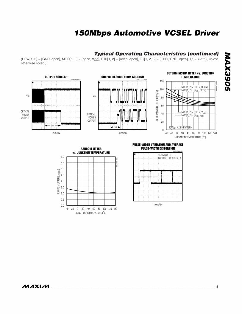
OUTPUT SQUELCHMAX3905 toc09
2μs/div
VIN
OPTICALPOWER
OUTPUT
tSQ
OUTPUT RESUME FROM SQUELCHMAX3905 toc10
40ns/div
VIN
OPTICALPOWER
OUTPUT
tRS0
20
40
60
80
100
120
-40 0-20 20 40 60 80 100 120 140
DETERMINISTIC JITTER vs. JUNCTIONTEMPERATURE
MAX
3905
toc1
1
JUNCTION TEMPERATURE (°C)
DETE
RMIN
ISTI
C JIT
TER
(ps P
-P)
MOD[1, 2] = [OPEN, OPEN]MOD[1, 2] = [VCC, OPEN]
MOD[1, 2] = [OPEN, VCC]MOD[1, 2] = [VCC, VCC]
150Mbps K28.5 PATTERN
2.0
5.5
4.5
4.0
3.5
3.0
2.5
5.0
6.0
-40 0-20 20 40 60 80 100 120 140
RANDOM JITTERvs. JUNCTION TEMPERATURE
MAX
3905
toc1
2
JUNCTION TEMPERATURE (°C)
RAND
OM JI
TTER
(ps R
MS)
PULSE-WIDTH VARIATION AND AVERAGEPULSE-WIDTH DISTORTION
10ns/div
MAX3905 toc13
45.1Mbps TTLBIPHASE-CODED DATA
Typical Operating Characteristics (continued) (LOW[1, 2] = [GND, open], MOD[1, 2] = [open, VCC], DT0[1, 2] = [open, open], TC[1, 2, 3] = [GND, GND, open], TA = +25°C, unlessotherwise noted.)
MA
X3
90
5
150Mbps Automotive VCSEL Driver
6 _______________________________________________________________________________________
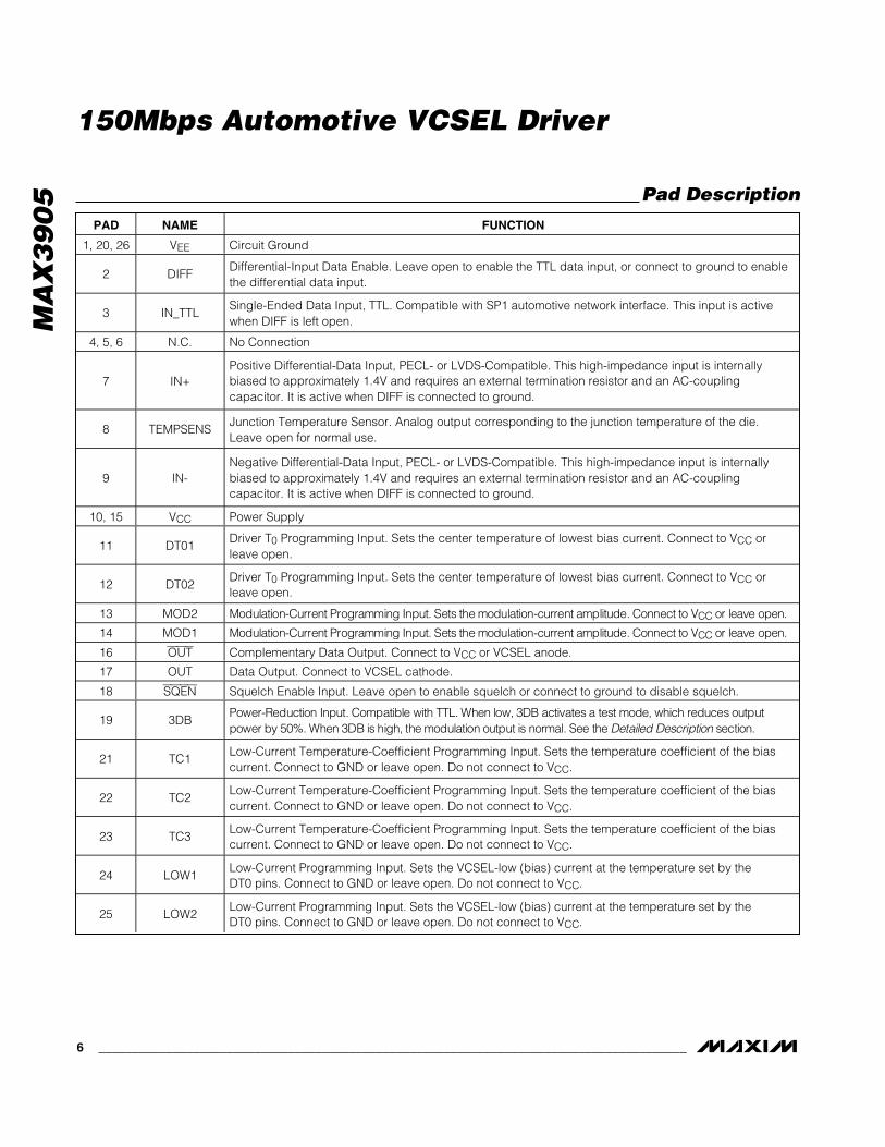
Pad Description
PAD NAME FUNCTION
1, 20, 26 VEE Circuit Ground
2 DIFFDifferential-Input Data Enable. Leave open to enable the TTL data input, or connect to ground to enablethe differential data input.
3 IN_TTLSingle-Ended Data Input, TTL. Compatible with SP1 automotive network interface. This input is activewhen DIFF is left open.
4, 5, 6 N.C. No Connection
7 IN+Positive Differential-Data Input, PECL- or LVDS-Compatible. This high-impedance input is internallybiased to approximately 1.4V and requires an external termination resistor and an AC-couplingcapacitor. It is active when DIFF is connected to ground.
8 TEMPSENSJunction Temperature Sensor. Analog output corresponding to the junction temperature of the die.Leave open for normal use.
9 IN-Negative Differential-Data Input, PECL- or LVDS-Compatible. This high-impedance input is internallybiased to approximately 1.4V and requires an external termination resistor and an AC-couplingcapacitor. It is active when DIFF is connected to ground.
10, 15 VCC Power Supply
11 DT01Driver T0 Programming Input. Sets the center temperature of lowest bias current. Connect to VCC orleave open.
12 DT02Driver T0 Programming Input. Sets the center temperature of lowest bias current. Connect to VCC orleave open.
13 MOD2 M od ul ati on- C ur r ent P r og r am m i ng Inp ut. S ets the m od ul ati on- cur r ent am p l i tud e. C onnect to V C C or l eave op en.
14 MOD1 M od ul ati on- C ur r ent P r og r am m i ng Inp ut. S ets the m od ul ati on- cur r ent am p l i tud e. C onnect to V C C or l eave op en.
16 OUT Complementary Data Output. Connect to VCC or VCSEL anode.
17 OUT Data Output. Connect to VCSEL cathode.
18 SQEN Squelch Enable Input. Leave open to enable squelch or connect to ground to disable squelch.
19 3DBP ow er - Red ucti on Inp ut. C om p ati b l e w i th TTL. W hen l ow , 3D B acti vates a test m od e, w hi ch r ed uces outp utp ow er b y 50%. W hen 3D B i s hi g h, the m od ul ati on outp ut i s nor m al . S ee the D etai l ed D escr i p ti on secti on.
21 TC1Low-Current Temperature-Coefficient Programming Input. Sets the temperature coefficient of the biascurrent. Connect to GND or leave open. Do not connect to VCC.
22 TC2Low-Current Temperature-Coefficient Programming Input. Sets the temperature coefficient of the biascurrent. Connect to GND or leave open. Do not connect to VCC.
23 TC3Low-Current Temperature-Coefficient Programming Input. Sets the temperature coefficient of the biascurrent. Connect to GND or leave open. Do not connect to VCC.
24 LOW1Low-Current Programming Input. Sets the VCSEL-low (bias) current at the temperature set by theDT0 pins. Connect to GND or leave open. Do not connect to VCC.
25 LOW2Low-Current Programming Input. Sets the VCSEL-low (bias) current at the temperature set by theDT0 pins. Connect to GND or leave open. Do not connect to VCC.
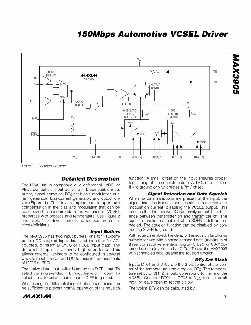
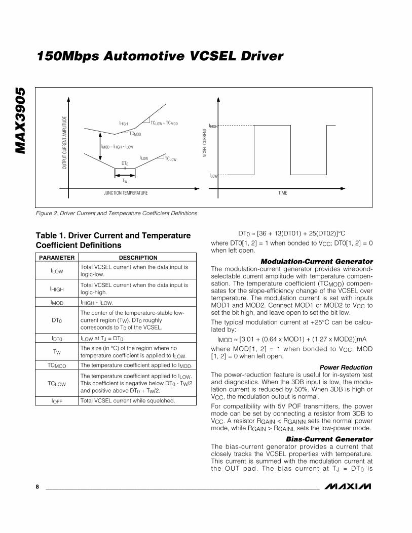
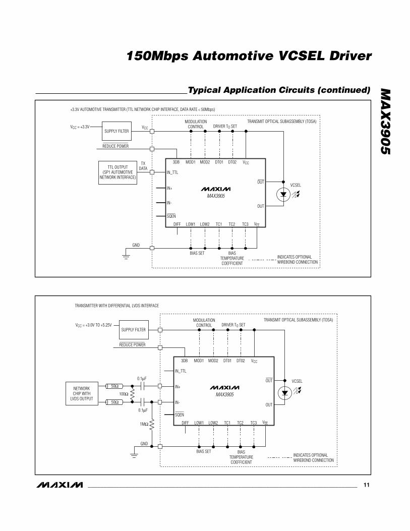
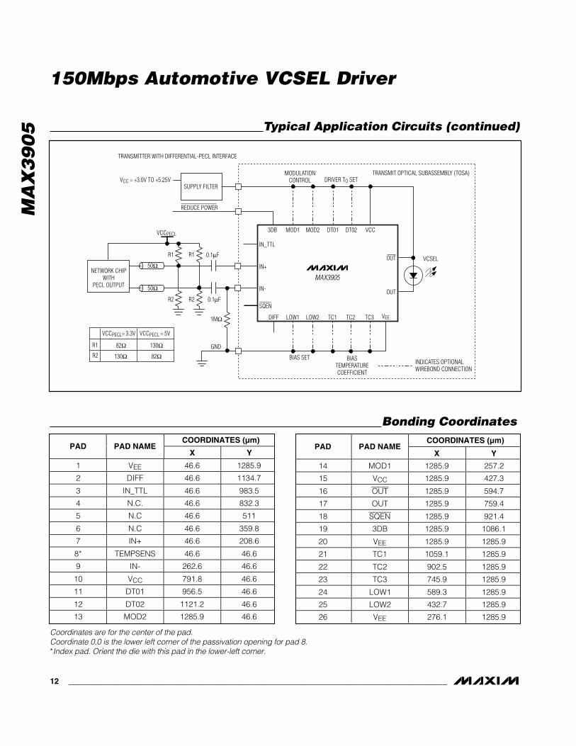
Detailed DescriptionThe MAX3905 is comprised of a differential LVDS- orPECL-compatible input buffer, a TTL-compatible inputbuffer, signal detection, DT0 set block, modulation-cur-rent generator, bias-current generator, and output dri-ver (Figure 1). The device implements temperaturecompensation in the bias and modulation that can becustomized to accommodate the variation of VCSELproperties with process and temperature. See Figure 2and Table 1 for driver current and temperature coeffi-cient definitions.
Input BuffersThe MAX3905 has two input buffers, one for TTL-com-patible DC-coupled input data, and the other for AC-coupled, differential LVDS or PECL input data. Thedifferential input is relatively high impedance. Thisallows external resistors to be configured in severalways to meet the AC- and DC-termination requirementsof LVDS or PECL.
The active data input buffer is set by the DIFF input. Toselect the single-ended TTL input, leave DIFF open. Toselect the differential input, connect DIFF to ground.
When using the differential input buffer, input noise canbe sufficient to prevent normal operation of the squelch
function. A small offset on the input ensures properfunctioning of the squelch feature. A 1MΩ resistor fromIN- to ground or VCC creates a 7mV offset.
Signal Detection and Data SquelchWhen no data transitions are present at the input, thesignal detection issues a squelch signal to the bias andmodulation current, disabling the VCSEL output. Thisensures that the receiver IC can easily detect the differ-ence between transmitter on and transmitter off. Thesquelch function is enabled when SQEN is left uncon-nected. The squelch function can be disabled by con-necting SQEN to ground.
With squelch enabled, the delay of the squelch function issuitable for use with biphase-encoded data (maximum ofthree consecutive identical digits (CIDs)) or 8B-/10B-encoded data (maximum five CIDs). To use the MAX3905with scrambled data, disable the squelch function.
DT0 Set BlockInputs DT01 and DT02 are the 2-bit control of the cen-ter of the temperature-stable region, DT0. The tempera-ture set by DT0[1, 2] should correspond to the T0 of theVCSEL. Connect DT01 or DT02 to VCC to set the bithigh, or leave open to set the bit low.
The typical DT0 can be calculated by:
MA
X3
90
5
150Mbps Automotive VCSEL Driver
_______________________________________________________________________________________ 7
IMOD
3DB MOD[1, 2]
OUT
VEE
VCC
TC[1, 2, 3] LOW[1, 2]
IMOD
TEMP
IBIAS
IBIAS
TEMP
DT0[1, 2]
DT0SET
TEMPSENS
K
GND
OPEN
DIFF
IN+
IN-
IN_TTL SIGNALDETECT
INPUTBUFFERS
SQEN
VCC
SQUELCH
OUT
OUTPUTDRIVER
MODULATIONCURRENT
GENERATOR
BIASCURRENT
GENERATOR
MAX3905
Figure 1. Functional Diagram
MA
X3
90
5
DT0 ≈ [36 + 13(DT01) + 25(DT02)]°C
where DT0[1, 2] = 1 when bonded to VCC; DT0[1, 2] = 0when left open.
Modulation-Current GeneratorThe modulation-current generator provides wirebond-selectable current amplitude with temperature compen-sation. The temperature coefficient (TCMOD) compen-sates for the slope-efficiency change of the VCSEL overtemperature. The modulation current is set with inputsMOD1 and MOD2. Connect MOD1 or MOD2 to VCC toset the bit high, and leave open to set the bit low.
The typical modulation current at +25°C can be calcu-lated by:
IMOD ≈ [3.01 + (0.64 x MOD1) + (1.27 x MOD2)]mA
where MOD[1, 2] = 1 when bonded to VCC; MOD [1, 2] = 0 when left open.
Power ReductionThe power-reduction feature is useful for in-system testand diagnostics. When the 3DB input is low, the modu-lation current is reduced by 50%. When 3DB is high orVCC, the modulation output is normal.
For compatibility with 5V POF transmitters, the powermode can be set by connecting a resistor from 3DB toVCC. A resistor RGAIN < RGAINN sets the normal powermode, while RGAIN > RGAINL sets the low-power mode.
Bias-Current GeneratorThe bias-current generator provides a current thatclosely tracks the VCSEL properties with temperature.This current is summed with the modulation current atthe OUT pad. The bias current at TJ = DT0 is
150Mbps Automotive VCSEL Driver
8 _______________________________________________________________________________________
Table 1. Driver Current and TemperatureCoefficient Definitions
PARAMETER DESCRIPTION
ILOWTotal VCSEL current when the data input islogic-low.
IHIGHTotal VCSEL current when the data input islogic-high.
IMOD IHIGH - ILOW.
DT0
The center of the temperature-stable low-current region (TW). DT0 roughlycorresponds to T0 of the VCSEL.
IDT0 ILOW at TJ = DT0.
TWThe size (in °C) of the region where notemperature coefficient is applied to ILOW.
TCMOD The temperature coefficient applied to IMOD.
TCLOW
The temperature coefficient applied to ILOW.This coefficient is negative below DT0 - TW/2and positive above DT0 + TW/2.
IOFF Total VCSEL current while squelched.
OUTP
UT C
URRE
NT A
MPL
ITUD
E
VCSE
L CU
RREN
T
JUNCTION TEMPERATURE TIME
IHIGH
ILOW
IHIGH
ILOW
IMOD = IHIGH - ILOW
TCMOD
TCLOW + TCMOD
TCLOWDTO
TW
Figure 2. Driver Current and Temperature Coefficient Definitions
programmed by the LOW1 and LOW2 inputs. ConnectLOW1 or LOW2 to ground to set the bit high, and leaveopen to set the bit low. Do not connect LOW1 or LOW2to VCC.
The typical low current at TJ = DT0 can be calculated by:
ILOW ≈ [1.8 + (0.37 x LOW1) + (0.73 x LOW2)]mA
where, LOW[1, 2] = 1 when bonded to ground; LOW[1, 2]= 0 when left open.
The temperature coefficient of the bias current is pro-grammed by the TC1, TC2, and TC3 inputs. ConnectTC1, TC2, or TC3 to ground to set the bit high, andleave open to set the bit low. Do not connect TC1, TC2,or TC3 to VCC.
The typical temperature coefficient of the bias currentcan be calculated by:
TCLOW ≈ [16 + (5 x TC1) + (11 x TC2) + (16 x TC3)]µA/°C
where, TC[1, 2, 3] = 1 when bonded to ground; TC[1, 2,3] = 0 when left open.
Junction-Temperature SensingA temperature sensor is incorporated into the MAX3905to aid in evaluation of thermal performance. TheTEMPSENS voltage is proportional to the die junctiontemperature (approximately -1.39mV per °C). The tem-perature of the die can be estimated as:
Output DriverThe OUT pad connects directly to the VCSEL cathode.The OUT pad must be connected to the VCSEL anodeor to VCC. The minimum instantaneous voltage on theOUT pad is 0.9V.
Applications InformationAdditional Design Assistance
For more information and design assistance, refer toMaxim Design Note HFDN-32.0: Output CurrentCalculator for the MAX3905.
Layout ConsiderationsLoad inductance on OUT and OUT should be matchedwithin 1.5nH to minimize both jitter and supply noisegeneration.
Wire BondingFor high-current density and reliable operation, theMAX3905 uses gold metalization. For best results, usegold-wire ball-bonding techniques. Exercise cautionwhen wedge bonding. Die size is 1.52mm x 1.52mm(60 mils x 60 mils), and die thickness is 300µm (12 mils). The bond-pad passivation opening is 93µm x93µm and bond-pad metal thickness is 1.2µm. Refer toMaxim Application Note HFAN-08.0.1: UnderstandingBonding Coordinates and Physical Die Size for addi-tional information on bondpad coordinates. Do notattempt to bond to the laser trim target.
Laser Safety and IEC 825Using the MAX3905 VCSEL driver alone does notensure that a transmitter design is compliant with IEC 825. The entire transmitter circuit and componentselections must be considered. Determine the level offault tolerance required by each application, and rec-ognize that Maxim products are not designed or autho-rized for use as components in systems intended forsurgical implant into the body, for applications intendedto support or sustain life, or for any other applicationwhere the failure of a Maxim product could create a sit-uation where personal injury or death may occur.
T C C V mV xC
mVTEMPSENS( ) ( )
.° ≈ ° °597
0 72
1-
MA
X3
90
5
150Mbps Automotive VCSEL Driver
_______________________________________________________________________________________ 9
MA
X3
90
5
150Mbps Automotive VCSEL Driver
10 ______________________________________________________________________________________
MAX3905
IN_TTL
VCC
1.5V
VEE
Figure 3. IN_TTL Equivalent Input Structure
MAX3905
IN+
IN-
VCC
VEE
5kΩ
5kΩ
1.4V
Figure 4. IN+/IN- Equivalent Input Structure
MAX3905
OUT
VCC
VEE
OUT
Figure 5. OUT/OUT Equivalent Output Structure
Chip InformationTRANSISTOR COUNT: 985
PROCESS: Silicon Bipolar GST-2
SUBSTRATE: Connected to VEE
DIE SIZE: 1.52mm x 1.52mm (60mils x 60mils)
DIE THICKNESS: 300µm (12mils)
MA
X3
90
5
150Mbps Automotive VCSEL Driver
______________________________________________________________________________________ 11
MAX3905
GND
TTL OUTPUT(SP1 AUTOMOTIVE
NETWORK INTERFACE)
REDUCE POWER
VCC = +3.3VSUPPLY FILTER
IN_TTL
IN+
DIFF
3DB
OUT
MOD2MOD1 DT02DT01 VCC
VCSEL
IN-
LOW1 LOW2 TC1 TC2 TC3
BIAS SET BIASTEMPERATURECOEFFICIENT
VEE
MODULATIONCONTROL DRIVER TO SET
INDICATES OPTIONALWIREBOND CONNECTION
SQEN
TRANSMIT OPTICAL SUBASSEMBLY (TOSA)
OUT
+3.3V AUTOMOTIVE TRANSMITTER (TTL NETWORK CHIP INTERFACE, DATA RATE < 50Mbps)
TXDATA
VCC
Typical Application Circuits (continued)
MAX3905
GND
REDUCE POWER
VCC = +3.0V TO +5.25VSUPPLY FILTER
IN_TTL
IN+50Ω
DIFF
3DB
OUT
MOD2MOD1 DT02DT01 VCC
VCSEL
IN-
LOW1 LOW2 TC1 TC2 TC3
BIAS SET BIASTEMPERATURECOEFFICIENT
VEE
MODULATIONCONTROL DRIVER TO SET
INDICATES OPTIONALWIREBOND CONNECTION
SQEN
TRANSMIT OPTICAL SUBASSEMBLY (TOSA)
OUT
NETWORKCHIP WITH
LVDS OUTPUT100Ω
0.1μF
50Ω
0.1μF
TRANSMITTER WITH DIFFERENTIAL LVDS INTERFACE
1MΩ
MA
X3
90
5
150Mbps Automotive VCSEL Driver
12 ______________________________________________________________________________________
MAX3905
GND
REDUCE POWER
VCC = +3.0V TO +5.25VSUPPLY FILTER
IN_TTL
IN+50Ω
VCCPECL
DIFF
3DB
OUT
MOD2MOD1 DT02DT01 VCC
VCSEL
IN-
LOW1 LOW2 TC1 TC2 TC3
BIAS SET BIASTEMPERATURECOEFFICIENT
VEE
MODULATIONCONTROL DRIVER TO SET
INDICATES OPTIONALWIREBOND CONNECTION
SQEN
TRANSMIT OPTICAL SUBASSEMBLY (TOSA)
OUT
NETWORK CHIPWITH
PECL OUTPUT
0.1μFR1
R2
R1
R2
50Ω
0.1μF
VCCPECL= 3.3V VCCPECL = 5V
R2
82Ω
130Ω
130Ω
82Ω
R1
TRANSMITTER WITH DIFFERENTIAL-PECL INTERFACE
1MΩ
Typical Application Circuits (continued)
COORDINATES (µm)PAD PAD NAME
X Y
1 VEE 46.6 1285.9
2 DIFF 46.6 1134.7
3 IN_TTL 46.6 983.5
4 N.C. 46.6 832.3
5 N.C 46.6 511
6 N.C 46.6 359.8
7 IN+ 46.6 208.6
8* TEMPSENS 46.6 46.6
9 IN- 262.6 46.6
10 VCC 791.8 46.6
11 DT01 956.5 46.6
12 DT02 1121.2 46.6
13 MOD2 1285.9 46.6
COORDINATES (µm)PAD PAD NAME
X Y
14 MOD1 1285.9 257.2
15 VCC 1285.9 427.3
16 OUT 1285.9 594.7
17 OUT 1285.9 759.4
18 SQEN 1285.9 921.4
19 3DB 1285.9 1086.1
20 VEE 1285.9 1285.9
21 TC1 1059.1 1285.9
22 TC2 902.5 1285.9
23 TC3 745.9 1285.9
24 LOW1 589.3 1285.9
25 LOW2 432.7 1285.9
26 VEE 276.1 1285.9
Coordinates are for the center of the pad.Coordinate 0,0 is the lower left corner of the passivation opening for pad 8.*Index pad. Orient the die with this pad in the lower-left corner.
Bonding Coordinates
MA
X3
90
5
150Mbps Automotive VCSEL Driver
Maxim cannot assume responsibility for use of any circuitry other than circuitry entirely embodied in a Maxim product. No circuit patent licenses areimplied. Maxim reserves the right to change the circuitry and specifications without notice at any time.
Maxim Integrated Products, 120 San Gabriel Drive, Sunnyvale, CA 94086 408-737-7600 ____________________ 13
© 2004 Maxim Integrated Products Printed USA is a registered trademark of Maxim Integrated Products.
Chip Topography
DIFF(PAD 2)
60mils
1.52mm
VEE(PAD 1)
IN_TTL(PAD 3)
N.C.(PAD 4)
N.C.(PAD 5)
N.C.(PAD 6)
IN+(PAD 7)
TEMPSENS(PAD 8)
IN-(PAD 9)
VCC(PAD 10)
DT01(PAD 11)
DT02(PAD 12)
MOD2(PAD 13)
MOD1(PAD 14)
VCC(PAD 15)
OUT(PAD 16)
OUT(PAD 17)
SQEN(PAD 18)
3DB(PAD 19)
VEE(PAD 20)
TC1(PAD 21)
TC2(PAD 22)
TC3(PAD 23)
LOW1(PAD 24)
LOW2(PAD 25)
VEE(PAD 26)
60mils1.52mm
LASERTRIM
TARGET