Embed Size (px)
Citation preview

Copyright Cirrus Logi(All Rights Reserhttp://www.cirrus.com
CDB8416
Evaluation Board for the CS8416 and CS8406
Features• CS8416 Digital Audio Receiver
• CS8406 Digital Audio Transmitter
• Receives and Transmits AES/EBU, S/PDIF, and EIAJ-340-compatible Digital Audio
• Analog and Digital 3.3 Volt Supply
• 3.3 to 5.0 Volt Logic Interface Supply
• Operates In Stand-alone Hardware Mode or Computer-controlled Software Mode
• Balanced and Unbalanced Inputs Available
DescriptionThe CDB8416 is designed to allow easy evaluation ofthe CS8416 and CS8406. The board is designed foreasy connection to an Audio Precision or other digital au-dio test system.
Input and output data may be set for either balanced us-ing the XLR connectors or unbalanced using the coax oroptical connectors.
Windows PC software provides a GUI to make configu-ration easy in Software Mode. The softwarecommunicates through the PC’s parallel port to controlthe internal registers so that all the possible softwaremodes of the CS8416 and CS8406 may be tested.
ORDERING INFORMATIONCDB8416 Evaluation Board
I
Optical In
Coax In
XLR In
Optical Out
Coax Out
XLR Out
CS8416 CS8406
Parallel Port to PC
c, Inc. 2009ved) APRIL ‘09
DS578DB3

CDB8416
TABLE OF CONTENTS
1. OVERVIEW ..........................................................................................................41.1 CS8416 and CS8406 ................................................................................................ 41.2 Parallel Port .............................................................................................................. 41.3 Serial Digital Audio Inputs ......................................................................................... 41.4 Serial Digital Audio Outputs ...................................................................................... 41.5 Three-wire (PCM) Serial Audio Input and Output ..................................................... 41.6 Crystal Oscillators ..................................................................................................... 41.7 LED Function Indicators ............................................................................................ 5
2. CONFIGURATION SETTINGS ............................................................................53. BOARD SETUP ...................................................................................................7
3.1 Power Supplies: ........................................................................................................ 73.2 Hardware Mode Settings: ......................................................................................... 73.3 Software Mode Settings: ........................................................................................... 7
3.3.1 Installing the Software: ................................................................................................. 73.3.2 Verifying Board Operation: ........................................................................................... 7
4. CDB8416.EXE USER'S GUIDE ...........................................................................84.1 Main Window ............................................................................................................ 8
5. BILL OF MATERIAL ..........................................................................................236. REVISION HISTORY .........................................................................................26
2 DS578DB3

CDB8416
LIST OF FIGURESFigure 1. CS8416 Control Panel ..................................................................................................... 8Figure 2. CS8406 Control Panel ..................................................................................................... 9Figure 3. Advanced Control Panel .................................................................................................. 9Figure 4. CDB8416 Block Diagram............................................................................................... 10Figure 5. Power............................................................................................................................. 11Figure 6. Digital Audio Inputs ........................................................................................................ 12Figure 7. Hardware Switches ........................................................................................................ 13Figure 8. Buffers............................................................................................................................ 14Figure 9. Clock Buffers.................................................................................................................. 15Figure 10. CS8416........................................................................................................................ 16Figure 11. CS8406........................................................................................................................ 17Figure 12. Digital Audio Outputs ................................................................................................... 18Figure 13. PC Control Interface .................................................................................................... 19Figure 14. Silkscreen Top ............................................................................................................. 20Figure 15. Top............................................................................................................................... 21Figure 16. Bottom.......................................................................................................................... 22
LIST OF TABLESTable 1. System Connections ........................................................................................................ 5Table 2. CDB8416 Jumper Settings ............................................................................................... 5Table 3. CDB8416 Switch Settings ................................................................................................ 6Table 4. CDB8416 Bill of Materials .............................................................................................. 23
DS578DB3 3

CDB8416
1. OVERVIEW
The CDB84166 evaluation board contains aCS8416 and a CS8406 and the supporting circuitrynecessary to operate them. The board provides bal-anced XLR and unbalanced optical and coaxial in-puts and outputs as outlined in the AES3 andIEC60958 standards. In Software Mode, the con-trol registers of the CS8416 and CS8406 are set bya Windows based program through the parallel portof a PC.
1.1 CS8416 and CS8406
The features and functions of the CS8416 and theCS8406 are described in their respective datasheets.
1.2 Parallel Port
To use the CS8416 and CS8406 on the board inSoftware Mode, the parallel port on the upper righthand side of the board should be connected to theparallel port of the PC running the CDB8416 con-trol software.
1.3 Serial Digital Audio Inputs
The left edge of the board is occupied by a row ofserial digital audio input connectors. In eitherHardware or Software Mode the user must selectwhich inputs are to be used via the switch setting,INPUT, on switch S3.
Set the switch to the open position to select theXLR balanced input which will use the RXP1 andRXN inputs of the CS8416.
Set the switch to the closed position to select theoptical/coaxial unbalanced inputs which will usethe RXP0 and RXP2 through RXP7 inputs of theCS8416. This will AC couple the RXN input toGND. Note that in Hardware Mode, only RXP0through RXP3 on the CS8416 are available for use.To select between the inputs in Hardware Mode,use the RXSEL0 and RXSEL1 switches on S3.
1.4 Serial Digital Audio Outputs
The right edge of the board is occupied by the serialdigital audio outputs. The optical S/PDIF output isalways enabled. The user may also choose to en-able either the coaxial S/PDIF output or the XLRAES3 output via jumper J11. These outputs aretransformer coupled.
1.5 Three-wire (PCM) Serial Audio Input and Output
Header J18 is provided so the user may access thethree wire serial audio ports of the receiver andtransmitter. The purpose of this port is to allow theuser to connect external circuitry such as a DAC,ADC, or DSP to the receiver and transmitter. Sig-nals going into or out of these headers should beoperated at VL+.
Setting switch S1-M/S in the open position sets theCS8416 as the master and the CS8406 as slave forLRCK and SCLK. Setting switch S1-M/S in theclosed position sets the CS8406 as the master andthe CS8416 as slave for LRCK and SCLK.
Setting switch S3-8416_PCM to the open positionwill turn off all of the input/output buffers for theCS8416. Setting switch S4-8406_PCM to the openposition will turn off all of the input/output buffersfor the CS8406. These switches allow the user toindependently set the input and output for theCS8416 and CS8406.
1.6 Crystal Oscillators
Oscillator Y1 provides the System Clock (OMCK)for the CS8416. The crystal oscillator on the boardis mounted in pin sockets that allow it to be re-moved or replaced. The board is shipped with a12.288 MHz crystal oscillator stuffed at Y1, settingthe output sampling rate to 48 kHz. Please refer tothe CS8416 data sheet for details on OMCK opera-tion.
4 DS578DB3

CDB8416
1.7 LED Function Indicators
Several LEDs are provided to indicate board func-tions. D9 indicates that power is present to theVD+/VA+ section of the CS8416 and CS8406.D11, D12, and D13 indicate the status of the
NV/RERR, AUDIO, and 96 kHz output of theCS8416 in Hardware Mode. See the CS8416 datasheet for an explanation of the conditions that acti-vate each of these outputs.
2. CONFIGURATION SETTINGS
CONNECTOR INPUT/OUTPUT SIGNAL PRESENTJ3 (+5V) Input +5 Volt Supply for supporting circuitry
J4 (GND) Input Ground connection from power supply
J5 (VL+) Input +3.3 to 5.0 Volt Digital Logic power for the CS8416 and CS8406
J6 (VD+/VA+) Input +3.3 Volt VD+/VA+ when not using the onboard regulator
J9, J16, J21 Input Digital Audio Interface coaxial input
OPT1-OPT4 Input Digital Audio Interface optical input
J2 Input Digital Audio Interface XLR input
J1 Input/Output Parallel port for connection to parallel port of PC
J20 Output Digital Audio Interface optical output
J19 Output Digital Audio Interface coaxial output
J10 Output Digital Audio Interface XLR output
J18 Input/Output I/O for CS8416 and CS8406 PCM data and clocks
Table 1. System Connections
JUMPER PURPOSE POSITION FUNCTION SELECTEDJ7 Selects between using a separate supply for
VL+ or using the +5 Supply.ADJUST
+5VUses J5 to supply from +3.3V to +5.0V for VL+ Uses J3 to supply +5V for VL+
J8 Selects between using a separate supply for VD+/VA+ or using the onboard +3.3V regulator.
REGADJUST
Uses the onboard +3.3V regulator for VD+/VA+ Uses J6 to provide the +3.3V supply for VD+/VA+
J12 Current measurement for CS8416 VA+ CLOSEDOPEN
Normal operationUse J13 to measure CS8416 VA+ current
J13 Current measurement for CS8416 VD+ CLOSEDOPEN
Normal operationUse J12 to measure CS8416 VD+ current
J17 Current measurement for CS8416 VL+ CLOSEDOPEN
Normal operationUse J16 to measure CS8416 VL+ current
J14 Current measurement for CS8406 VD+ CLOSEDOPEN
Normal operationUse J14 to measure CS8406 VD+ current
J15 Current measurement for CS8406 VL+ CLOSEDOPEN
Normal operationUse J15 to measure CS8406 VL+ current
J11 Selects between coaxial or XLR output XLRCOAX
Selects XLR output on J10 Selects coaxial output on J19
Table 2. CDB8416 Jumper Settings
DS578DB3 5
CDB8416
SWITCH PURPOSE POSITION FUNCTION SELECTEDS1-H/S Selects Hardware or Software Mode for
CS8416 and CS8406.OPEN
CLOSEDCS8416 and CS8406 are in Hardware Mode.CS8416 and CS8406 are in Software Mode.
S1-M/S Selects Master or Slave Mode for LRCK and SCLK.
OPENCLOSED
CS8416 Master. CS8406 Slave. CS8416 Master. CS8406 Slave.
S1-SFMT1S1-SFMT0
Selects serial audio output format for the CS8416 and input format for the CS8406.
00011011
Left Justified 24 bitI2S 24 bit Right Justified 24 bitDirect AES3 (CS8416)Right Justified 16 bit (CS8406)
S3-INPUT Selects CS8416 receiver input topology. OPENCLOSED
XLR balanced input.Optical/Coaxial unbalanced input.
S3-8416_PCM Controls the input/output buffers for the CS8416 serial audio port.
OPENCLOSED
CS8416 I/O buffers off.CS8416 I/O buffers on.
S3-NVSEL Selects between NVERR and RERR. OPENCLOSED
NVERR output selected.RERR output selected.
S3-RXSEL1S3-RXSEL0
Hardware mode RXP input channel select for the CS8416.
00011011
RXP0 SelectedRXP1 Selected RXP2 SelectedRXP3 Selected
S3-TXSEL1S3-TXSEL0
Hardware mode TX pass through channel select for the CS8416
00011011
RXP0 pass through to TXRXP1 pass through to TX RXP2 pass through to TX RXP3 pass through to TX
S4-8406_PCM Controls the input/output buffers for the CS8406 serial audio port.
OPENCLOSED
CS8406 I/O buffers off.CS8406 I/O buffers on.
S4-TCBLD Selects the direction of TCBL for the CS8406.
OPENCLOSED
TCBL set to output.TCBL set to input.
S4-CEN Selects input method for channel status, user, and validity data.
OPENCLOSED
Mode B is selected.Mode A is selected.
Table 3. CDB8416 Switch Settings
6 DS578DB3

CDB8416
3. BOARD SETUP
3.1 Power Supplies:
1) Verify that all power supplies are off beforemaking connections.
2) Connect a +3.3 V DC power supply to theVD+/VA+ (J6) binding post and place jumperJ8 in the ADJUST position. This connectionmay be omitted by setting J8 to the REG posi-tion. VD+/VA+ will be derived from the on-board +3.3V regulator.
3) Connect a +3.3 V to +5.0 V DC power supplyto the VL+ (J5) binding post and place jumperJ7 in the ADJUST position. This connectionmay be omitted by setting J7 to the +5 V posi-tion. VL+ will be derived from the +5 V bind-ing post.
4) Connect a +5.0 V DC power supply to the +5 V(J3) binding post.
5) Connect the common ground of the power sup-plies to the GND (J4) binding post.
6) Apply power to the board. D9 should illumi-nate indicating power is applied to VD+/VA+.
3.2 Hardware Mode Settings:
1) Place switch S1-H/S in the OPEN position.
2) Place switches S3-INPUT, S3-8416_PCM, S3-NVSEL, S3-RXSEL1, S3-RXSEL0, S3-TXSEL1, S3-TXSEL0, S1-M/S, S1-SFMT1,S1-SFMT0, S4-8406_PCM, S4-TCBLD, S4-CEN to the appropriate positions.
3) Press and release the RESET switch S3. Theboard should now be setup for use in HardwareMode.
3.3 Software Mode Settings:
1) Place switch S1-H/S in the CLOSED position.
2) Place switches S1-M/S, S3-INPUT, S3-8416_PCM, and S4-8406_PCM to the appro-priate positions. All other switch setting do not
effect Software Mode operation.
3) Press and release the RESET switch S2. Theboard should now be setup for use in Softwaremode.
4) Connect a DB-25 parallel port cable from thePC’s parallel port to J1 on the CDB8416.
3.3.1 Installing the Software:1) Create a directory called CDB8416 anywhere
on your system.
2) Copy CDB8416.exe from the included CD intothis directory.
3) Run port95nt.exe from the CD. After runningthe program the system will need to be restart-ed.
4) If desired, create a shortcut to CDB8416.exe onyour desktop. You should now be able to runCDB8416.exe.
5) Double-click on CDB8416.exe or its shortcut.
6) Click on the button on the lower right labeled“Advanced”.
7) Select the LPT port you are using to connect tothe CDB8416.
8) Shut down the application, reset the board, andthen restart the application.
3.3.2 Verifying Board Operation:1) In the “CS8416 AES Receiver Controls” win-
dow, select the check box “Enable InternalClocks” (enables the RUN bit in the ClockControl register).
2) In the “CS8406 AES Transmitter Controls”window, select the check box “Enable Clocks”(enables the RUN bit in the Clock Control reg-ister).
3) In the “CS8416 AES Receiver Controls” win-dow, select the check box “GenerateSCLK/LRCK”. Make sure that switch S1-M/Sis in the OPEN position.
DS578DB3 7

CDB8416
4) Check the performance of the board by doingan FFT with a -1 dBFS 1 kHz sine wave for in-put at a 48 kHz sample rate using the optical in-put and optical output.
4. CDB8416.EXE USER'S GUIDE
4.1 Main Window
The main window of the CDB8416 Control Appli-cation allows the user to view the configuration ofthe CS8416. Clicking the left mouse button on the
CS8406 Controls button will bring up a controlpanel containing all the register bits relevant to thatpart.
Clicking on the Advanced button at the lower rightbrings up the Advanced Options control panel.Within the Advanced Options you may read andwrite hex values into specified registers in eitherpart. Changes made on the CS8406 or CS8416 con-trol panels will also be immediately reflected in theMain Window, so you may wish to arrange them sothat they do not obscure each other.
Figure 1. CS8416 Control Panel
8 DS578DB3

CDB8416
Figure 2. CS8406 Control Panel
Figure 3. Advanced Control Panel
DS578DB3 9
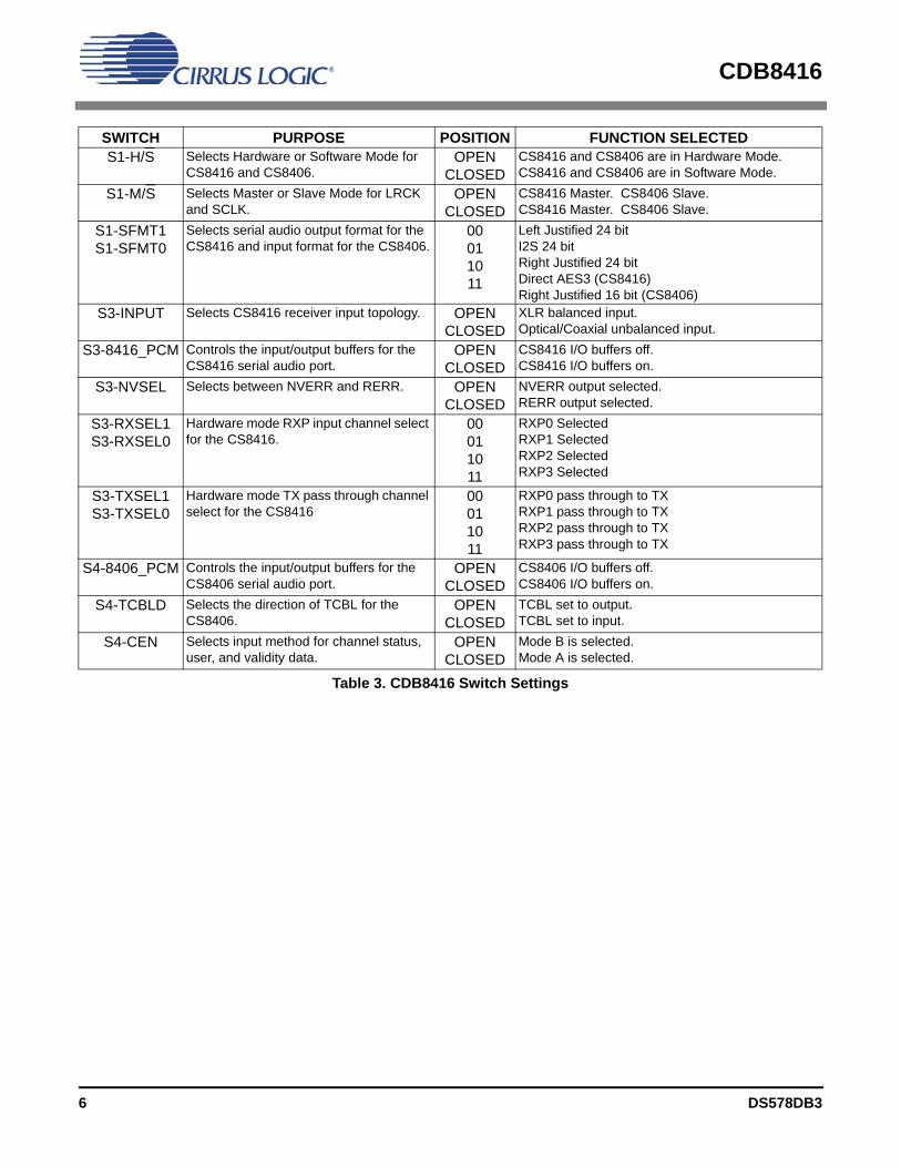
CDB8416
RX In
put
CS84
16
PC
Inte
rface
PCM
Buffe
rsCS
8406
TX O
utpu
t
Fig
ure
4.
CD
B84
16
Blo
ck
Dia
gra
m
10 DS578DB3

CDB8416
5. BILL OF MATERIAL
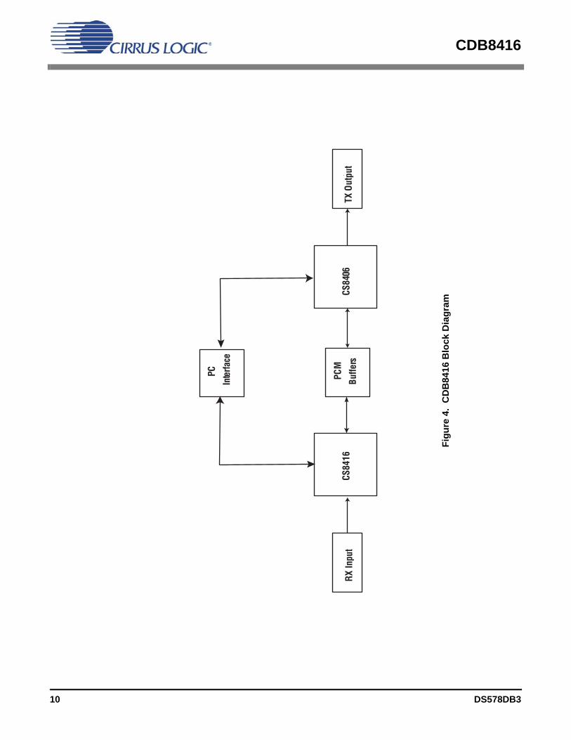
Item Qty Reference Part Number Manufacturer Description1 41 C1 C2 C4 C5 C8 C9 C10
C11 C12 C14 C16 C18 C19 C20 C21 C23 C25 C26 C29 C30 C31 C32 C34 C35 C36 C38 C42 C44 C47 C51 C53 C59 C61 C64 C66 C67 C68 C69 C70 C72 C75
C0805C104J5RAC KEMET CAP, 0.1UF, X7R, 0805, 50V, 5%
2 5 C3 C6 C7 C13 C49 ECE-V1AA101WR PANASONIC3 7 C15 C22 C27 C40 C54
C71 C76C0805C103K5RAC KEMET CAP, 0.01UF, X7R, 0805,
50V, 10%4 1 C17 C0805C561J5RAC KEMET CAP, 560PF, X7R, 0805,
50V, 5%5 13 C24 C28 C37 C39 C45
C46 C50 C55 C62 C63 C65 C73 C74
C0805C102J5RAC KEMET CAP, 1000pF, X7R, 0805, 50V, 5%
6 2 C33 C56 C0805C103J5RAC KEMET CAP, 0.01UF, X7R, 0805, 50V, 5%
7 4 C41 C43 C52 C60 ECE-V1CS100SR PANASONIC CAP, 10uF, ELEC, VS SERIES, SMT CASE-A, 16V, 20%
8 1 C48 C0805C220J5GAC KEMET CAP, 22PF, COG, 0805, 50V, 5%
9 1 C57 C1206C224J5RAC KEMET CAP, 0.22UF, X7R, 1206, 50V, 5%
10 1 C58 C1206C103J3GAC KEMET CAP, 0.01UF, COG, 1206, 25V, 5%
11 9 D1 D2 D3 D4 D5 D6 D7 D8 D10
MBR0520LT1 MOTOROLA SCHOTTKY POWER RECTIFIER, SMT SOD123 CASE
12 1 D9 CMD28-21VYC/TR8/T1 CHICAGO MINIA-TURE
LED, SMT, YELLOW
13 2 D11 D12 CMD28-21SRC/TR8/T1 CHICAGO MINIA-TURE
LED, SMT, RED
14 1 D13 CMD28-21VGC/TR8/T1 CHICAGO MINIA-TURE
LED, SMT, GREEN
15 5 GND1 GND2 GND3 GND4 GND5
JUMPER WIRE
16 4 GND6 GND7 GND8 GND9
DO NOT POPULATE
17 1 J1 747842-6 AMP CONNECTOR, DB25, MALE, RT. ANGLE, 0.318 MNT
18 1 J2 NC3FD-H NEUTRIK CONNECTOR, XLR, FEMALE
19 1 J3 111-0102-001 E.F. JOHNSON BINDING POST, RED20 1 J4 111-0103-001 E.F. JOHNSON BINDING POST, BLACK21 1 J5 111-0104-001 E.F. JOHNSON BINDING POST, GREEN22 1 J6 111-0110-001 E.F. JOHNSON BINDING POST, BLUE23 3 J7 J8 J11 TSW-103-07-G-S SAMTEC STAKE HEADER, 3X1,
0.1" CTR, GOLD
Table 4. CDB8416 Bill of Materials
DS578DB3 23

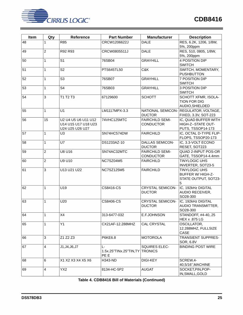
CDB8416
24 4 J9 J16 J19 J21 ARJ-2018-1 A/D ELECTRONICS RCA JACK - RIGHT ANGLE, GOLD PLATED
25 1 J10 NC3MD-H NEUTRIK CONNECTOR, XLR, MALE
26 5 J12 J13 J14 J15 J17 TSW-102-07-G-S SAMTEC STAKE HEADER, 2X1, 0.1"CTR, GOLD
27 1 J18 TSW-105-07-G-D SAMTEC STAKE HEADER, 5X2, 0.1"CTR, GOLD
28 1 J20 TOTX173 TOSHIBA OPTICAL TOSLINK TRANSMITTER
29 4 L1 L2 L3 L5 ELJ-FA470KF PANASONIC INDUCTOR, 47uH, 1210, TYPE FA, 10%
30 1 L4 FB73-226 J.W.MILLER FERRITE BEAD, 0-40MHz
31 4 OPT1 OPT2 OPT3 OPT4 TORX173 TOSHIBA OPTICAL TOSLINK RECEIVER
32 3 R1 R3 R32 CRCW0805100FT DALE RES, 10-OHM, 0805, 1/10W, 1%. 100ppm
33 2 R2 R95 CRCW1206271J DALE RES, 270, 1206, 1/8W, 5%, 200ppm
34 2 R4 R64 CRCW080590R9F DALE RES, 90.9 OHMS, 0805, 1/10W, 1%. 100ppm
35 12 R5 R6 R7 R8 R9 R10 R11 R12 R14 R15 R16 R17
CRCW08052001F DALE RES, 2K, 0805, 1/10W, 1%. 100ppm
36 1 R13 CRCW08051651F DALE RES, 1.65K, 0805, 1/10W, 1%. 100ppm
37 23 R18 R19 R20 R21 R22 R23 R24 R25 R26 R27 R28 R29 R31 R58 R66 R67 R71 R84 R86 R87 R88 R89 R90
CRCW0805473J DALE RES, 47K, 0805, 1/10W, 5%, 200ppm
38 1 R30 NP-RES-0805 N/A DO NOT POPULATE39 10 R33 R35 R37 R42 R45
R47 R76 R80 R82 R83CRCW08051000F DALE RES, 100-OHM, 0805,
1/10W, 1%. 100ppm. 100ppm
40 3 R34 R65 R96 CRCW080575R0F DALE RES, 75.0 OHMS, 0805, 1/10W, 1%. 100ppm
41 1 R36 CRCW080556R2FKEA DALE RES, 56.2 OHMS, 0805, 1/8W, 1%. 100ppm
42 8 R38 R39 R53 R54 R68 R75 R91 R94
ERJ-6GEYJ330V PANASONIC RES, 33 OHMS, 1/10W,0805, 5%
43 19 R40 R41 R43 R44 R46 R48 R56 R57 R60 R62 R69 R70 R72 R73 R74 R77 R78 R79 R81
CRCW0805000FT DALE RES, 0-OHM, 0805
44 5 R49 R50 R51 R52 R61 CRCW08051R0J DALE RES, 1 OHM, 0805, 1/8W, 5%, 300ppm
45 1 R55 NP-RES-1206 N/A DO NOT POPULATE46 1 R59 CRCW12061001F DALE RES, 1K, 1206, 1/8W,
1%, 100ppm47 1 R63 CRCW0805348RFKEA DALE RES, 348 OHMS, 0805,
1/8W, 1%. 100ppm
Item Qty Reference Part Number Manufacturer Description
Table 4. CDB8416 Bill of Materials (Continued)
24 DS578DB3
CDB8416
48 1 R85 CRCW1206622J DALE RES, 6.2K, 1206, 1/8W, 5%, 200ppm
49 2 R92 R93 CRCW0805511J DALE RES, 510, 0805, 1/8W, 5%, 200ppm
50 1 S1 76SB04 GRAYHILL 4 POSITION DIP SWITCH
51 1 S2 PTS645TL50 C&K SWITCH, MOMENTARY, PUSHBUTTON
52 1 S3 76SB07 GRAYHILL 7 POSITION DIP SWITCH
53 1 S4 76SB03 GRAYHILL 3 POSITION DIP SWITCH
54 3 T1 T2 T3 67129600 SCHOTT SCHOTT XFMR, ISOLA-TION FOR DIG AUDIO,SHIELDED
55 1 U1 LM1117MPX-3.3 NATIONAL SEMICON-DUCTOR
REGULATOR, VOLTAGE, FIXED, 3.3V, SOT-223
56 15 U2 U4 U5 U6 U11 U12 U14 U15 U17 U18 U23 U24 U25 U26 U27
74VHC125MTC FAIRCHILD SEMI-CONDUCTOR
IC, QUAD BUFFER WITH HIGH-Z--STATE OUT-PUTS, TSSOP14-173
57 1 U3 SN74HC574DW FAIRCHILD IC, OCTAL D-TYPE FLIP-FLOPS, TSSOP20-173
58 1 U7 DS1233AZ-10 DALLAS SEMICON-DUCTOR
IC, 3.3-VOLT ECONO RESET, SOT223
59 2 U8 U16 SN74AC32MTC FAIRCHILD SEMI-CONDUCTOR
QUAD 2-INPUT POS-OR GATE, TSSOP14-4.4mm
60 2 U9 U10 NC7SZ04M5 FAIRCHILD TINYLOGIC UHS INVERTER, SOT23-5
61 3 U13 U21 U22 NC7SZ125M5 FAIRCHILD TINYLOGIC UHS BUFFER W/ HIGH-Z-STATE OUTPUT, SOT23-5
62 1 U19 CS8416-CS CRYSTAL SEMICON-DUCTOR
IC, 192kHz DIGITAL AUDIO RECEIVER, SO28-300
63 1 U20 CS8406-CS CRYSTAL SEMICON-DUCTOR
IC, 192kHz DIGITAL AUDIO TRANSMITTER, SO28-300
64 1 X4 313-6477-032 E.F.JOHNSON STANDOFF, #4-40,.25 HEX x .875 LG
65 1 Y1 CX21AF-12.288MHZ CAL CRYSTAL OSCILLATOR, 12.288MHZ, FULLSIZE CASE
66 3 Z1 Z2 Z3 P6KE6.8 MOTOROLA TRANSIENT SUPPRES-SOR, 6.8V
67 4 J1,J4,J6,J7 L-1.5x.25”TINx.25”TIN,TYPE E
SQUIRES ELEC-TRONICS
BINDING POST WIRE
68 6 X1 X2 X3 X4 X5 X6 H343-ND DIGI-KEY SCREW,4-40,5/16”,MACHINE
69 4 YX2 8134-HC-5P2 AUGAT SOCKET,PIN,POP-IN,SMALL,GOLD
Item Qty Reference Part Number Manufacturer Description
Table 4. CDB8416 Bill of Materials (Continued)
DS578DB3 25

CDB8416
6. REVISION HISTORY
Release Changes
DB3-Updated Figure 12.-Updated Item 41 and 47 in Section 5 Bill of Material.
Contacting Cirrus Logic SupportFor all product questions and inquiries contact a Cirrus Logic Sales Representative. To find one nearest you go to www.cirrus.com
IMPORTANT NOTICE
Cirrus Logic, Inc. and its subsidiaries ("Cirrus") believe that the information contained in this document is accurate and reliable. However, the informationis subject to change without notice and is provided "AS IS" without warranty of any kind (express or implied). Customers are advised to obtain the latestversion of relevant information to verify, before placing orders, that information being relied on is current and complete. All products are sold subject tothe terms and conditions of sale supplied at the time of order acknowledgment, including those pertaining to warranty, indemnification, and limitation ofliability. No responsibility is assumed by Cirrus for the use of this information, including use of this information as the basis for manufacture or sale of anyitems, or for infringement of patents or other rights of third parties. This document is the property of Cirrus and by furnishing this information, Cirrusgrants no license, express or implied under any patents, mask work rights, copyrights, trademarks, trade secrets or other intellectual property rights. Cir-rus owns the copyrights associated with the information contained herein and gives consent for copies to be made of the information only for use withinyour organization with respect to Cirrus integrated circuits or other products of Cirrus. This consent does not extend to other copying such as copying forgeneral distribution, advertising or promotional purposes, or for creating any work for resale.
CERTAIN APPLICATIONS USING SEMICONDUCTOR PRODUCTS MAY INVOLVE POTENTIAL RISKS OF DEATH, PERSONAL INJURY, ORSEVERE PROPERTY OR ENVIRONMENTAL DAMAGE (“CRITICAL APPLICATIONS”). CIRRUS PRODUCTS ARE NOT DESIGNED, AUTHORIZEDOR WARRANTED FOR USE IN PRODUCTS SURGICALLY IMPLANTED INTO THE BODY, AUTOMOTIVE SAFETY OR SECURITY DEVICES, LIFESUPPORT PRODUCTS OR OTHER CRITICAL APPLICATIONS. INCLUSION OF CIRRUS PRODUCTS IN SUCH APPLICATIONS IS UNDERSTOODTO BE FULLY AT THE CUSTOMER’S RISK AND CIRRUS DISCLAIMS AND MAKES NO WARRANTY, EXPRESS, STATUTORY OR IMPLIED,INCLUDING THE IMPLIED WARRANTIES OF MERCHANTABILITY AND FITNESS FOR PARTICULAR PURPOSE, WITH REGARD TO ANY CIRRUSPRODUCT THAT IS USED IN SUCH A MANNER. IF THE CUSTOMER OR CUSTOMER’S CUSTOMER USES OR PERMITS THE USE OF CIRRUSPRODUCTS IN CRITICAL APPLICATIONS, CUSTOMER AGREES, BY SUCH USE, TO FULLY INDEMNIFY CIRRUS, ITS OFFICERS, DIRECTORS,EMPLOYEES, DISTRIBUTORS AND OTHER AGENTS FROM ANY AND ALL LIABILITY, INCLUDING ATTORNEYS’ FEES AND COSTS, THAT MAYRESULT FROM OR ARISE IN CONNECTION WITH THESE USES.
Cirrus Logic, Cirrus, and the Cirrus Logic logo designs are trademarks of Cirrus Logic, Inc. All other brand and product names in this document may betrademarks or service marks of their respective owners.
26 DS578DB3


![BRYSTON LIMITED WARRANTYBP26].pdf · regarding the operation of your amplifier. We con- ... Power Supply via its Power switch ~ a toggle switch ... All inputs and outputs employ fully](https://img.pdfslide.us/doc/110x75/5b09abe17f8b9a5f6d8e4ccc/bryston-limited-bp26pdfregarding-the-operation-of-your-amplifier-we-con-.jpg)