Embed Size (px)
Citation preview
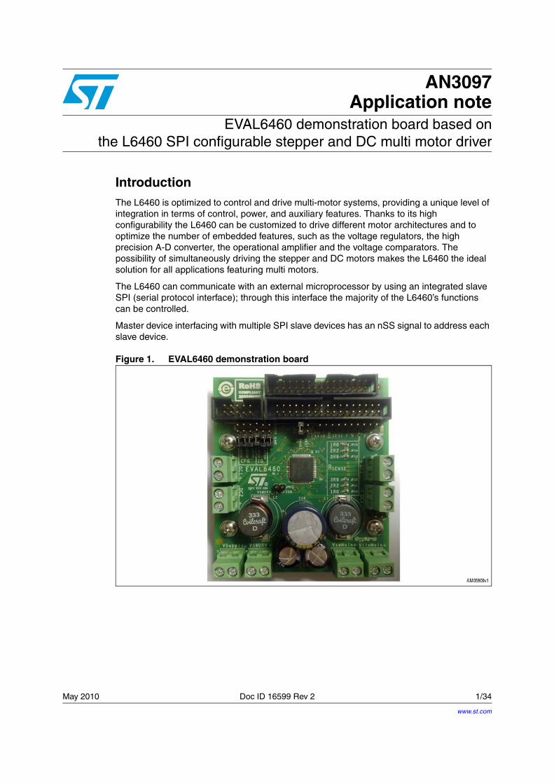
May 2010 Doc ID 16599 Rev 2 1/34
AN3097Application note
EVAL6460 demonstration board based onthe L6460 SPI configurable stepper and DC multi motor driver
IntroductionThe L6460 is optimized to control and drive multi-motor systems, providing a unique level of integration in terms of control, power, and auxiliary features. Thanks to its high configurability the L6460 can be customized to drive different motor architectures and to optimize the number of embedded features, such as the voltage regulators, the high precision A-D converter, the operational amplifier and the voltage comparators. The possibility of simultaneously driving the stepper and DC motors makes the L6460 the ideal solution for all applications featuring multi motors.
The L6460 can communicate with an external microprocessor by using an integrated slave SPI (serial protocol interface); through this interface the majority of the L6460’s functions can be controlled.
Master device interfacing with multiple SPI slave devices has an nSS signal to address each slave device.
Figure 1. EVAL6460 demonstration board
www.st.com
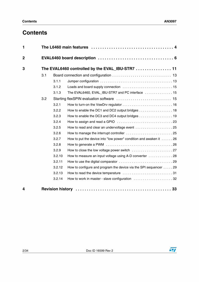
Contents AN3097
2/34 Doc ID 16599 Rev 2
Contents
1 The L6460 main features . . . . . . . . . . . . . . . . . . . . . . . . . . . . . . . . . . . . . 4
2 EVAL6460 board description . . . . . . . . . . . . . . . . . . . . . . . . . . . . . . . . . . 6
3 The EVAL6460 controlled by the EVAL_IBU-STR7 . . . . . . . . . . . . . . . . 11
3.1 Board connection and configuration . . . . . . . . . . . . . . . . . . . . . . . . . . . . . 13
3.1.1 Jumper configuration . . . . . . . . . . . . . . . . . . . . . . . . . . . . . . . . . . . . . . . 13
3.1.2 Loads and board supply connection . . . . . . . . . . . . . . . . . . . . . . . . . . . 15
3.1.3 The EVAL6460, EVAL_IBU-STR7 and PC interface . . . . . . . . . . . . . . . 15
3.2 Starting flexSPIN evaluation software . . . . . . . . . . . . . . . . . . . . . . . . . . . 15
3.2.1 How to turn-on the VswDrv regulator . . . . . . . . . . . . . . . . . . . . . . . . . . . 16
3.2.2 How to enable the DC1 and DC2 output bridges . . . . . . . . . . . . . . . . . . 18
3.2.3 How to enable the DC3 and DC4 output bridges . . . . . . . . . . . . . . . . . . 19
3.2.4 How to assign and read a GPIO . . . . . . . . . . . . . . . . . . . . . . . . . . . . . . 23
3.2.5 How to read and clear an undervoltage event . . . . . . . . . . . . . . . . . . . . 25
3.2.6 How to manage the interrupt controller . . . . . . . . . . . . . . . . . . . . . . . . . 25
3.2.7 How to put the device into "low power" condition and awaken it . . . . . . 26
3.2.8 How to generate a PWM . . . . . . . . . . . . . . . . . . . . . . . . . . . . . . . . . . . . 26
3.2.9 How to close the low voltage power switch . . . . . . . . . . . . . . . . . . . . . . 27
3.2.10 How to measure an input voltage using A-D converter . . . . . . . . . . . . . 28
3.2.11 How to use the digital comparator . . . . . . . . . . . . . . . . . . . . . . . . . . . . . 29
3.2.12 How to configure and program the device via the SPI sequencer . . . . . 29
3.2.13 How to read the device temperature . . . . . . . . . . . . . . . . . . . . . . . . . . . 31
3.2.14 How to work in master - slave configuration . . . . . . . . . . . . . . . . . . . . . 32
4 Revision history . . . . . . . . . . . . . . . . . . . . . . . . . . . . . . . . . . . . . . . . . . . 33
AN3097 List of figures
Doc ID 16599 Rev 2 3/34
List of figures
Figure 1. EVAL6460 demonstration board. . . . . . . . . . . . . . . . . . . . . . . . . . . . . . . . . . . . . . . . . . . . . . 1Figure 2. EVAL6460 demonstration board schematic . . . . . . . . . . . . . . . . . . . . . . . . . . . . . . . . . . . . . 8Figure 3. EVAL6460 component placement (top and bottom). . . . . . . . . . . . . . . . . . . . . . . . . . . . . . 10Figure 4. EVAL6460 layer layout . . . . . . . . . . . . . . . . . . . . . . . . . . . . . . . . . . . . . . . . . . . . . . . . . . . . 10Figure 5. EVAL_IBU-STR7 board . . . . . . . . . . . . . . . . . . . . . . . . . . . . . . . . . . . . . . . . . . . . . . . . . . . 11Figure 6. EVAL_IBU-STR7 schematic board. . . . . . . . . . . . . . . . . . . . . . . . . . . . . . . . . . . . . . . . . . . 12Figure 7. Jumper startup configuration . . . . . . . . . . . . . . . . . . . . . . . . . . . . . . . . . . . . . . . . . . . . . . . 13Figure 8. Jumper device ID . . . . . . . . . . . . . . . . . . . . . . . . . . . . . . . . . . . . . . . . . . . . . . . . . . . . . . . . 13Figure 9. nAwake driving source . . . . . . . . . . . . . . . . . . . . . . . . . . . . . . . . . . . . . . . . . . . . . . . . . . . . 14Figure 10. Awake input . . . . . . . . . . . . . . . . . . . . . . . . . . . . . . . . . . . . . . . . . . . . . . . . . . . . . . . . . . . . 14Figure 11. Stepper current sense resistor value . . . . . . . . . . . . . . . . . . . . . . . . . . . . . . . . . . . . . . . . . 14Figure 12. nRESET feedback capability . . . . . . . . . . . . . . . . . . . . . . . . . . . . . . . . . . . . . . . . . . . . . . . 15Figure 13. FlexSPIN evaluation software - start window . . . . . . . . . . . . . . . . . . . . . . . . . . . . . . . . . . . 16Figure 14. L6460 block diagram . . . . . . . . . . . . . . . . . . . . . . . . . . . . . . . . . . . . . . . . . . . . . . . . . . . . . 16Figure 15. Switching regulator controller . . . . . . . . . . . . . . . . . . . . . . . . . . . . . . . . . . . . . . . . . . . . . . . 17Figure 16. Enable switching regulator controller . . . . . . . . . . . . . . . . . . . . . . . . . . . . . . . . . . . . . . . . . 17Figure 17. Current DAC block diagram . . . . . . . . . . . . . . . . . . . . . . . . . . . . . . . . . . . . . . . . . . . . . . . . 18Figure 18. Bridge 1 and 2: PWM and operation mode selection . . . . . . . . . . . . . . . . . . . . . . . . . . . . . 18Figure 19. Bridge 1 and 2 configuration. . . . . . . . . . . . . . . . . . . . . . . . . . . . . . . . . . . . . . . . . . . . . . . . 19Figure 20. Bridge 3 and 4 configuration. . . . . . . . . . . . . . . . . . . . . . . . . . . . . . . . . . . . . . . . . . . . . . . . 20Figure 21. Bridge 3 and 4: PWM and operation mode selection . . . . . . . . . . . . . . . . . . . . . . . . . . . . . 20Figure 22. Bridge 3 and 4 configuration: stepper controller . . . . . . . . . . . . . . . . . . . . . . . . . . . . . . . . . 21Figure 23. Bipolar stepper configuration window . . . . . . . . . . . . . . . . . . . . . . . . . . . . . . . . . . . . . . . . . 22Figure 24. GPIO12 and GPIO13 configuration . . . . . . . . . . . . . . . . . . . . . . . . . . . . . . . . . . . . . . . . . . 23Figure 25. GPIOs block diagram . . . . . . . . . . . . . . . . . . . . . . . . . . . . . . . . . . . . . . . . . . . . . . . . . . . . . 24Figure 26. GPIO14 A-to-D conversion . . . . . . . . . . . . . . . . . . . . . . . . . . . . . . . . . . . . . . . . . . . . . . . . . 24Figure 27. Supervisory and reset manager window. . . . . . . . . . . . . . . . . . . . . . . . . . . . . . . . . . . . . . . 25Figure 28. Interrupt controller diagram. . . . . . . . . . . . . . . . . . . . . . . . . . . . . . . . . . . . . . . . . . . . . . . . . 26Figure 29. GPIO11 configuration for PWM . . . . . . . . . . . . . . . . . . . . . . . . . . . . . . . . . . . . . . . . . . . . . 27Figure 30. Low power switch 1 enable. . . . . . . . . . . . . . . . . . . . . . . . . . . . . . . . . . . . . . . . . . . . . . . . . 27Figure 31. Low power switch 1 disable . . . . . . . . . . . . . . . . . . . . . . . . . . . . . . . . . . . . . . . . . . . . . . . . 28Figure 32. A-D block diagram . . . . . . . . . . . . . . . . . . . . . . . . . . . . . . . . . . . . . . . . . . . . . . . . . . . . . . . 28Figure 33. Conversion source selection. . . . . . . . . . . . . . . . . . . . . . . . . . . . . . . . . . . . . . . . . . . . . . . . 28Figure 34. Digital comparator block diagram . . . . . . . . . . . . . . . . . . . . . . . . . . . . . . . . . . . . . . . . . . . . 29Figure 35. FlexSPIN sequencer window . . . . . . . . . . . . . . . . . . . . . . . . . . . . . . . . . . . . . . . . . . . . . . . 30Figure 36. Thermal manager window . . . . . . . . . . . . . . . . . . . . . . . . . . . . . . . . . . . . . . . . . . . . . . . . . 32
The L6460 main features AN3097
4/34 Doc ID 16599 Rev 2
1 The L6460 main features
Four widely configurable full bridges:
● Bridges 1 and 2:
– Diagonal Ron: 0.6 Ω typ.
– Max. operative current = 2.5 A
● Bridges 3 and 4:
– Diagonal Ron: 0.85 Ω typ.
– Max. operative current = 1.5 A
Possible configurations for each bridge:
● Bridge 1:
– DC motor driver
– Super DC (bridge 1and 2 parallel to form super-bridge 1).
– 2 independent half bridges
– 1 super half bridge (bridge 1 side A and bridge 1 side B parallel to form super-half bridge1)
– 2 independent switches (high or low side)
– 1 super-switch (high or low side)
● Bridge 2 has the same configurations as bridge 1
● Bridge 3 has the same configurations as bridge 1 (bridge 3 and 4 paralleled to form super-bridge 2) plus the following:
– ½ stepper motor driver
– 2 buck regulators (VAUX1_SW, VAUX2_SW)
– Super-buck regulator (VAUX1//2_SW)
● Bridge 4 has the same configurations as bridge 1 plus the following:
– ½ stepper motor driver
– 1 super buck regulator (VAUX3_SW)
– Battery charger.
The L6460 is intended to maximize the use of its components, so when an internal circuit is not in use it can be used for other applications.
Bridge 3, for example, can be used as a full bridge or to implement two switching regulators with synchronous rectification. To obtain this flexibility the L6460 includes two independent regulation loops that can be used for these regulators; when the bridge is used as a motor driver, the two regulation loops can be redirected on general purpose I/Os to allow the possibility of assembling a switching regulator by just adding an external FET.
AN3097 The L6460 main features
Doc ID 16599 Rev 2 5/34
● One buck type switching regulator (VswMain) with:
– Output regulated voltage range: 1-5 V
– Max output load current: 3.0 A
– Internal output power DMOS
– Internal soft-start sequence
– Internal PWM generation
– Switching frequency: ~250 kHz
– Pulse skipping strategy control
● One switching regulator controller (VSWDRV) with:
– Output regulated voltage range: 1-30 V
– Selectable current limitation
– Internal PWM generation
– Pulse skipping strategy control
● One linear regulator (VlinMain) that can be used to generate low current/low ripple voltages. This regulator can be used to drive an external bipolar pass transistor to generate high current/low ripple output voltages
● One bi-directional serial Interface with address detection so that different ICs can share the same data bus
● Integrated power sequencing and supervisory functions with fault signaling through serial interface and an external reset pin
● Fourteen general purpose I/Os that can be used to drive/read internal/external analog/logic signals
● One 8 or 9 bit A-D converter (100 kS/s @ 9 bits, 200 kS/s @ 8 bits). This can be used to measure most of the internal signals of the input pins and a voltage proportional to the IC temperature
● Current sink DAC:
– Three output current ranges: up to 0.64/6.4/64 mA.
– 64 (6 bits programmable) available current levels for each range
– 5 V output tolerant
● Two operational amplifiers:
– 3.3 V supply, rail to rail input compatibility, internally compensated
– They can have all pins externally accessible or can be internally configured as a buffer to make internal reference voltages available outside of the chip
– Unity gain bandwidth greater than 1 MHz
– They can also be set as comparators with 3.3 V input compatibility and low offset.
● Two 3.3 V pass switches with 0.6 Ω typ RDS(on) and short-circuit detected
● Programmable Watchdog function
● Thermal shutdown protection with thermal warning capability
● Very low power dissipation in low-power mode (~35 mW)
EVAL6460 board description AN3097
6/34 Doc ID 16599 Rev 2
2 EVAL6460 board description
This demonstration board shows an example of an application which the L6460 is able to manage:
● 2 DC motors
● 1 stepper motor
● 3 power supplies: 1.2 V, 3.3 V and 12 V.
Table 1 summarizes the operating rating specification of the application, Table 2 lists the connectors and jumpers available on the board and their function; Figure 2 shows the electrical schematic and Table 3 shows the BOM list.
Table 1. EVAL6460: operating ratings specification
Parameter Value
Supply voltage range (VSupply) 13 to 38 Vdc
Low voltage pins power supply (VGPIO_SPI) 3.3 V (1)
1. Generated by the L6460 main switching regulator
Internal 3.3 V regulator (V3V3) 3.3 V
Main linear regulator output voltage 1.2 V
Main switching regulator output voltage 3.3 V
Switching regulator output voltage (switching controller) 12 V (2)
2. To enable by user (see 5.2.1 How to turn-on the VswDrv regulator)
Operating junction temperature range -25 to +125°C
AN3097 EVAL6460 board description
Doc ID 16599 Rev 2 7/34
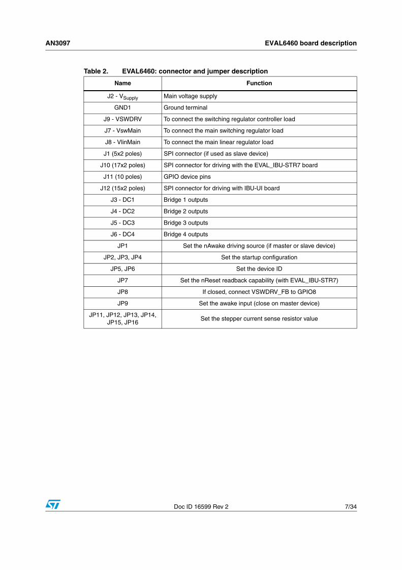
Table 2. EVAL6460: connector and jumper description
Name Function
J2 - VSupply Main voltage supply
GND1 Ground terminal
J9 - VSWDRV To connect the switching regulator controller load
J7 - VswMain To connect the main switching regulator load
J8 - VlinMain To connect the main linear regulator load
J1 (5x2 poles) SPI connector (if used as slave device)
J10 (17x2 poles) SPI connector for driving with the EVAL_IBU-STR7 board
J11 (10 poles) GPIO device pins
J12 (15x2 poles) SPI connector for driving with IBU-UI board
J3 - DC1 Bridge 1 outputs
J4 - DC2 Bridge 2 outputs
J5 - DC3 Bridge 3 outputs
J6 - DC4 Bridge 4 outputs
JP1 Set the nAwake driving source (if master or slave device)
JP2, JP3, JP4 Set the startup configuration
JP5, JP6 Set the device ID
JP7 Set the nReset readback capability (with EVAL_IBU-STR7)
JP8 If closed, connect VSWDRV_FB to GPIO8
JP9 Set the awake input (close on master device)
JP11, JP12, JP13, JP14, JP15, JP16
Set the stepper current sense resistor value
EVAL6460 board description AN3097
8/34 Doc ID 16599 Rev 2
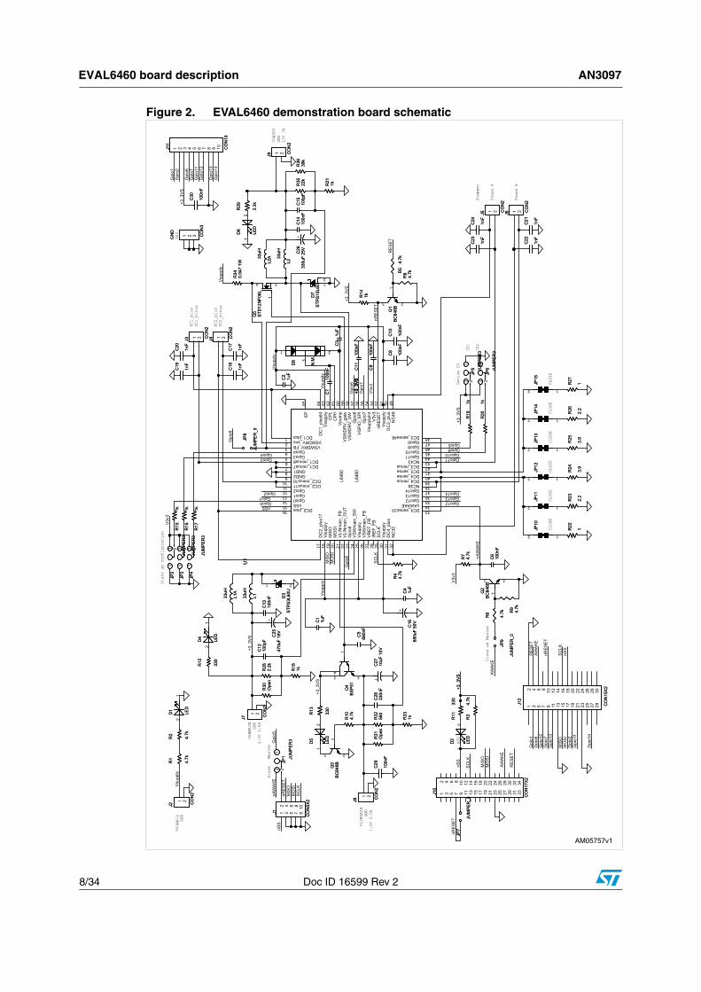
Figure 2. EVAL6460 demonstration board schematic
AN3097 EVAL6460 board description
Doc ID 16599 Rev 2 9/34
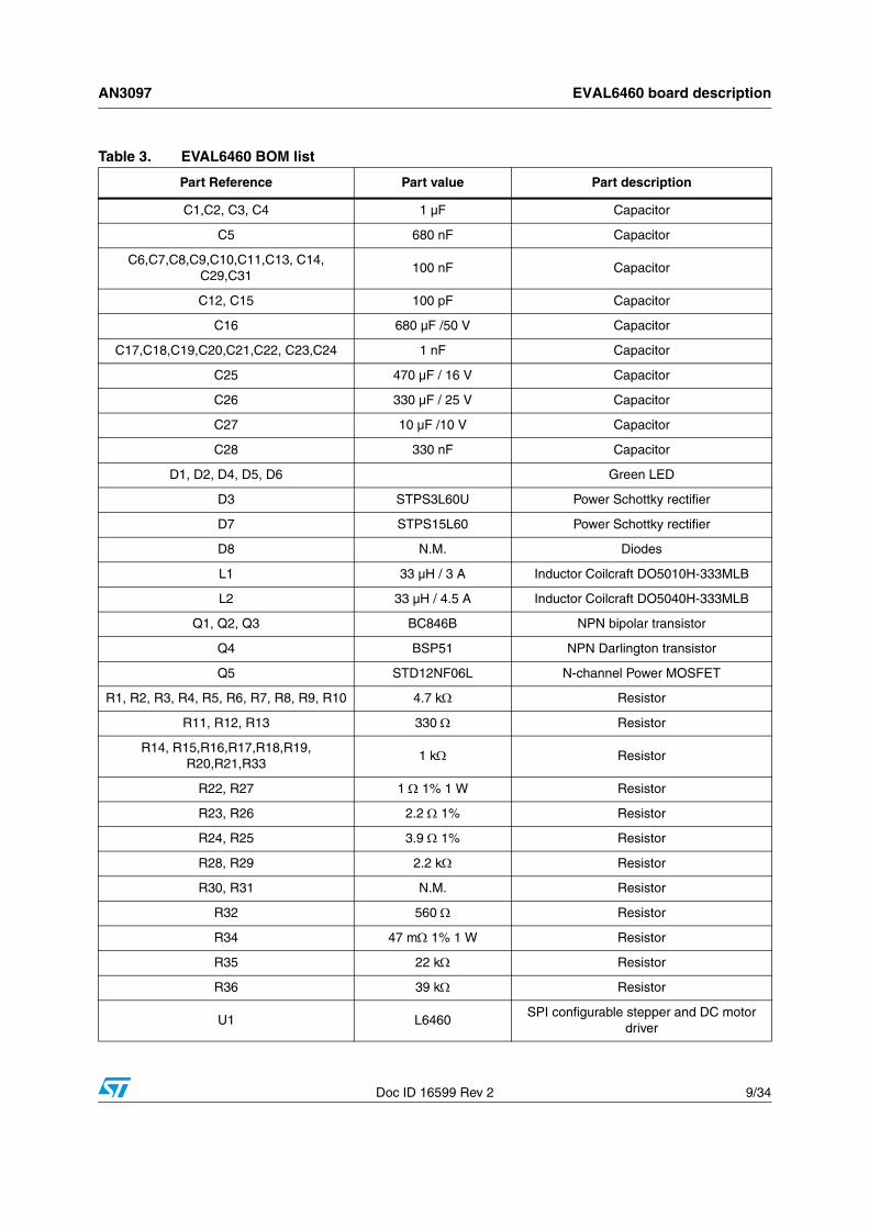
Table 3. EVAL6460 BOM list
Part Reference Part value Part description
C1,C2, C3, C4 1 µF Capacitor
C5 680 nF Capacitor
C6,C7,C8,C9,C10,C11,C13, C14, C29,C31
100 nF Capacitor
C12, C15 100 pF Capacitor
C16 680 µF /50 V Capacitor
C17,C18,C19,C20,C21,C22, C23,C24 1 nF Capacitor
C25 470 µF / 16 V Capacitor
C26 330 µF / 25 V Capacitor
C27 10 µF /10 V Capacitor
C28 330 nF Capacitor
D1, D2, D4, D5, D6 Green LED
D3 STPS3L60U Power Schottky rectifier
D7 STPS15L60 Power Schottky rectifier
D8 N.M. Diodes
L1 33 µH / 3 A Inductor Coilcraft DO5010H-333MLB
L2 33 µH / 4.5 A Inductor Coilcraft DO5040H-333MLB
Q1, Q2, Q3 BC846B NPN bipolar transistor
Q4 BSP51 NPN Darlington transistor
Q5 STD12NF06L N-channel Power MOSFET
R1, R2, R3, R4, R5, R6, R7, R8, R9, R10 4.7 kΩ Resistor
R11, R12, R13 330 Ω Resistor
R14, R15,R16,R17,R18,R19, R20,R21,R33
1 kΩ Resistor
R22, R27 1 Ω 1% 1 W Resistor
R23, R26 2.2 Ω 1% Resistor
R24, R25 3.9 Ω 1% Resistor
R28, R29 2.2 kΩ Resistor
R30, R31 N.M. Resistor
R32 560 Ω Resistor
R34 47 mΩ 1% 1 W Resistor
R35 22 kΩ Resistor
R36 39 kΩ Resistor
U1 L6460 SPI configurable stepper and DC motor
driver
EVAL6460 board description AN3097
10/34 Doc ID 16599 Rev 2
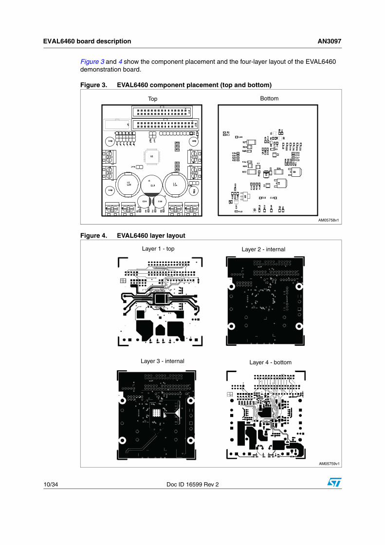
Figure 3 and 4 show the component placement and the four-layer layout of the EVAL6460 demonstration board.
Figure 3. EVAL6460 component placement (top and bottom)
Figure 4. EVAL6460 layer layout
AN3097 The EVAL6460 controlled by the EVAL_IBU-STR7
Doc ID 16599 Rev 2 11/34
3 The EVAL6460 controlled by the EVAL_IBU-STR7
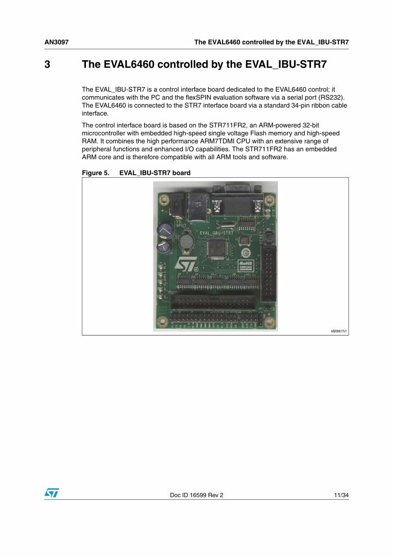
The EVAL_IBU-STR7 is a control interface board dedicated to the EVAL6460 control; it communicates with the PC and the flexSPIN evaluation software via a serial port (RS232). The EVAL6460 is connected to the STR7 interface board via a standard 34-pin ribbon cable interface.
The control interface board is based on the STR711FR2, an ARM-powered 32-bit microcontroller with embedded high-speed single voltage Flash memory and high-speed RAM. It combines the high performance ARM7TDMI CPU with an extensive range of peripheral functions and enhanced I/O capabilities. The STR711FR2 has an embedded ARM core and is therefore compatible with all ARM tools and software.
Figure 5. EVAL_IBU-STR7 board
The EVAL6460 controlled by the EVAL_IBU-STR7 AN3097
12/34 Doc ID 16599 Rev 2
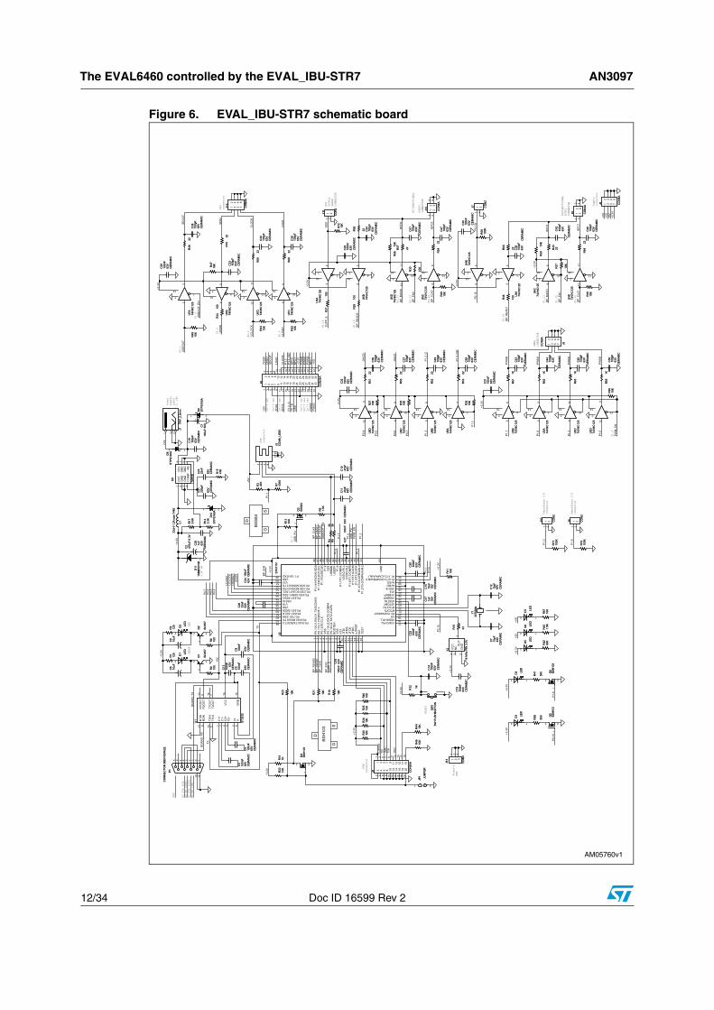
Figure 6. EVAL_IBU-STR7 schematic board
AN3097 The EVAL6460 controlled by the EVAL_IBU-STR7
Doc ID 16599 Rev 2 13/34
3.1 Board connection and configurationIn this section the configuration of the EVAL6460 board, how to connect the board supply, loads, and interface it to a PC through the EVAL_IBU-STR7 is shown.
3.1.1 Jumper configuration
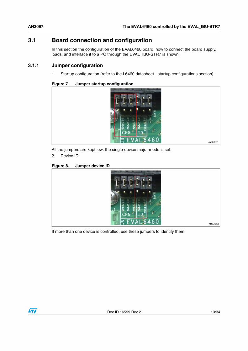
1. Startup configuration (refer to the L6460 datasheet - startup configurations section).
Figure 7. Jumper startup configuration
All the jumpers are kept low: the single-device major mode is set.
2. Device ID
Figure 8. Jumper device ID
If more than one device is controlled, use these jumpers to identify them.
The EVAL6460 controlled by the EVAL_IBU-STR7 AN3097
14/34 Doc ID 16599 Rev 2
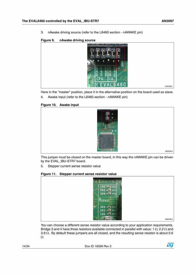
3. nAwake driving source (refer to the L6460 section - nAWAKE pin)
Figure 9. nAwake driving source
Here in the "master" position, place it in the alternative position on the board used as slave.
4. Awake input (refer to the L6460 section - nAWAKE pin)
Figure 10. Awake input
This jumper must be closed on the master board, in this way the nAWAKE pin can be driven by the EVAL_IBU-STR7 board.
5. Stepper current sense resistor value
Figure 11. Stepper current sense resistor value
You can choose a different sense resistor value according to your application requirements. Bridge 3 and 4 have three resistors available connected in parallel with value: 1 Ω, 2.2 Ω and 3.9 Ω.. By default these jumpers are all closed, and the resulting sense resistor is about 0.6 Ω.
AN3097 The EVAL6460 controlled by the EVAL_IBU-STR7
Doc ID 16599 Rev 2 15/34
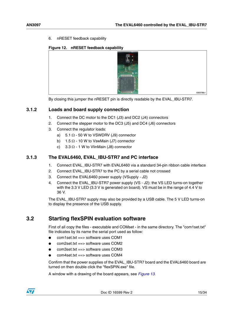
6. nRESET feedback capability
Figure 12. nRESET feedback capability
By closing this jumper the nRESET pin is directly readable by the EVAL_IBU-STR7.
3.1.2 Loads and board supply connection
1. Connect the DC motor to the DC1 (J3) and DC2 (J4) connectors
2. Connect the stepper motor to the DC3 (J5) and DC4 (J6) connectors
3. Connect the regulator loads:
a) 5.1 Ω - 50 W to VSWDRV (J9) connector
b) 1.5 Ω - 10 W to VswMain (J7) connector
c) 3.3 Ω - 1 W to VlinMain (J8) connector
3.1.3 The EVAL6460, EVAL_IBU-STR7 and PC interface
1. Connect EVAL_IBU-STR7 with EVAL6460 via a standard 34-pin ribbon cable interface
2. Connect EVAL_IBU-STR7 to the PC by a serial cable not crossed
3. Connect the EVAL6460 power supply (VSupply - J2)
4. Connect the EVAL_IBU-STR7 power supply (VS - J2): the VS LED turns-on together with the 3.3 V LED (3.3 V is generated on board). VS must be in the range of 4.4 V to 36 V.
The EVAL_IBU-STR7 supply may also be provided by a USB cable. The 5 V LED turns-on to display the presence of the USB supply.
3.2 Starting flexSPIN evaluation softwareFirst of all copy the files - executable and COMset - in the same directory. The "com1set.txt" file indicates by its name the serial port used as follow:
● com1set.txt ==> software uses COM1
● com2set.txt ==> software uses COM2
● com3set.txt ==> software uses COM3
● com4set.txt ==> software uses COM4
Confirm that the power supplies of the EVAL_IBU-STR7 board and the EVAL6460 board are turned on then double click the "flexSPIN.exe" file.
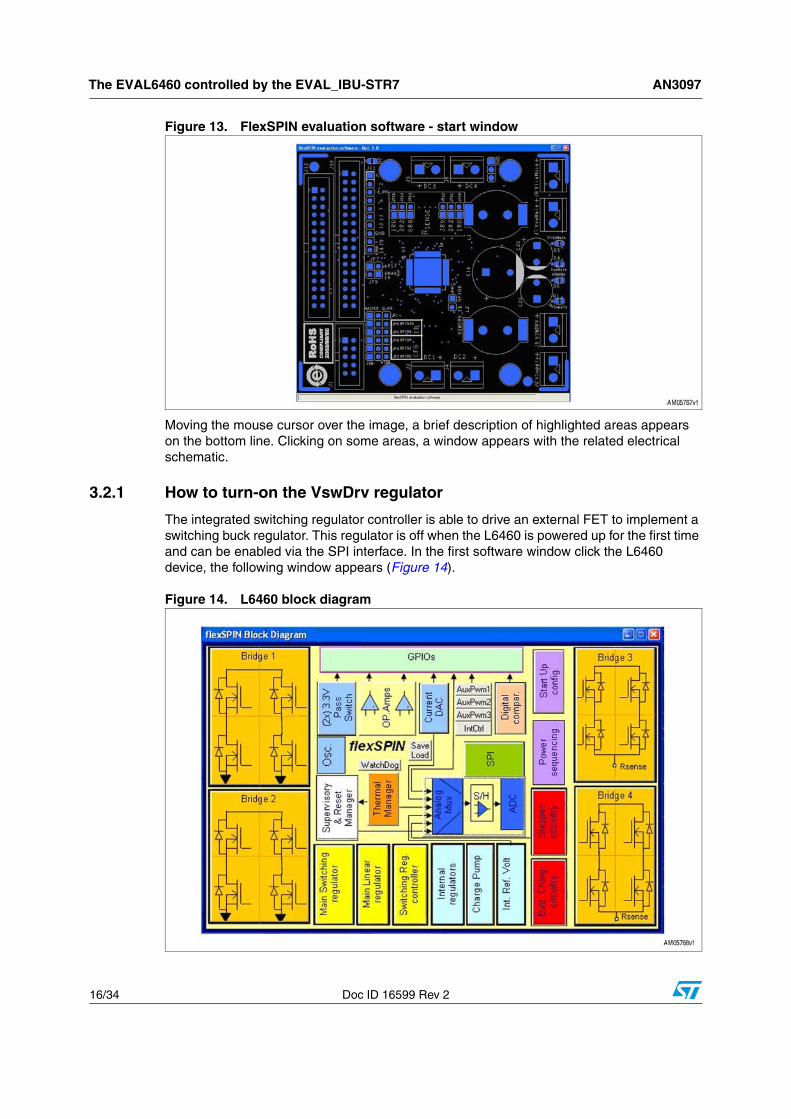
A window with a drawing of the board appears, see Figure 13.
The EVAL6460 controlled by the EVAL_IBU-STR7 AN3097
16/34 Doc ID 16599 Rev 2
Figure 13. FlexSPIN evaluation software - start window
Moving the mouse cursor over the image, a brief description of highlighted areas appears on the bottom line. Clicking on some areas, a window appears with the related electrical schematic.
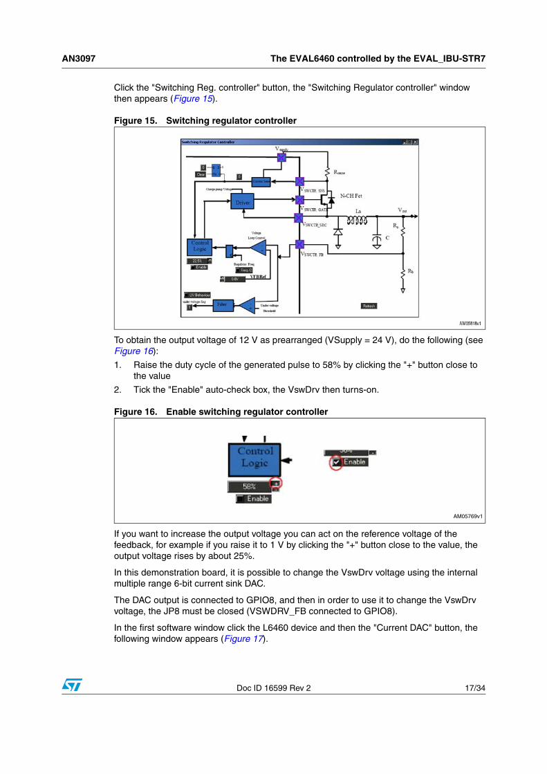
3.2.1 How to turn-on the VswDrv regulator
The integrated switching regulator controller is able to drive an external FET to implement a switching buck regulator. This regulator is off when the L6460 is powered up for the first time and can be enabled via the SPI interface. In the first software window click the L6460 device, the following window appears (Figure 14).
Figure 14. L6460 block diagram
AN3097 The EVAL6460 controlled by the EVAL_IBU-STR7
Doc ID 16599 Rev 2 17/34
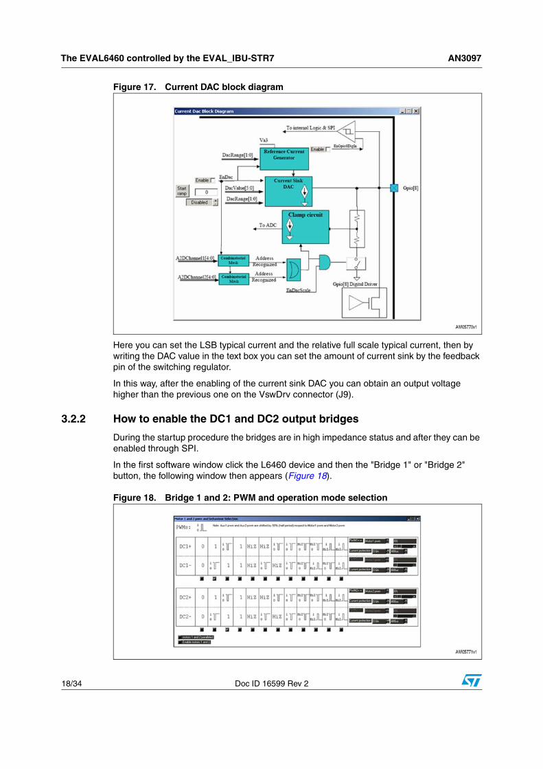
Click the "Switching Reg. controller" button, the "Switching Regulator controller" window then appears (Figure 15).
Figure 15. Switching regulator controller
To obtain the output voltage of 12 V as prearranged (VSupply = 24 V), do the following (see Figure 16):
1. Raise the duty cycle of the generated pulse to 58% by clicking the "+" button close to the value
2. Tick the "Enable" auto-check box, the VswDrv then turns-on.
Figure 16. Enable switching regulator controller
If you want to increase the output voltage you can act on the reference voltage of the feedback, for example if you raise it to 1 V by clicking the "+" button close to the value, the output voltage rises by about 25%.
In this demonstration board, it is possible to change the VswDrv voltage using the internal multiple range 6-bit current sink DAC.
The DAC output is connected to GPIO8, and then in order to use it to change the VswDrv voltage, the JP8 must be closed (VSWDRV_FB connected to GPIO8).
In the first software window click the L6460 device and then the "Current DAC" button, the following window appears (Figure 17).
The EVAL6460 controlled by the EVAL_IBU-STR7 AN3097
18/34 Doc ID 16599 Rev 2
Figure 17. Current DAC block diagram
Here you can set the LSB typical current and the relative full scale typical current, then by writing the DAC value in the text box you can set the amount of current sink by the feedback pin of the switching regulator.
In this way, after the enabling of the current sink DAC you can obtain an output voltage higher than the previous one on the VswDrv connector (J9).
3.2.2 How to enable the DC1 and DC2 output bridges
During the startup procedure the bridges are in high impedance status and after they can be enabled through SPI.
In the first software window click the L6460 device and then the "Bridge 1" or "Bridge 2" button, the following window then appears (Figure 18).
Figure 18. Bridge 1 and 2: PWM and operation mode selection
AN3097 The EVAL6460 controlled by the EVAL_IBU-STR7
Doc ID 16599 Rev 2 19/34
By ticking the auto-check boxes, you can configure the operation mode of the single half bridge outputs. The options available are:
● '0': Hold the output low (low side power on)
● '1': Hold the output high (high side power on)
● HiZ: high impedance status (high and low side off)
● PWM_1-0: the output is alternatively in status '0' or '1'
● PWM_HiZ-0: the output is alternatively in status 'HiZ' or '0'
● PWM_1-HiZ: the output is alternatively in status '1' or 'HiZ'
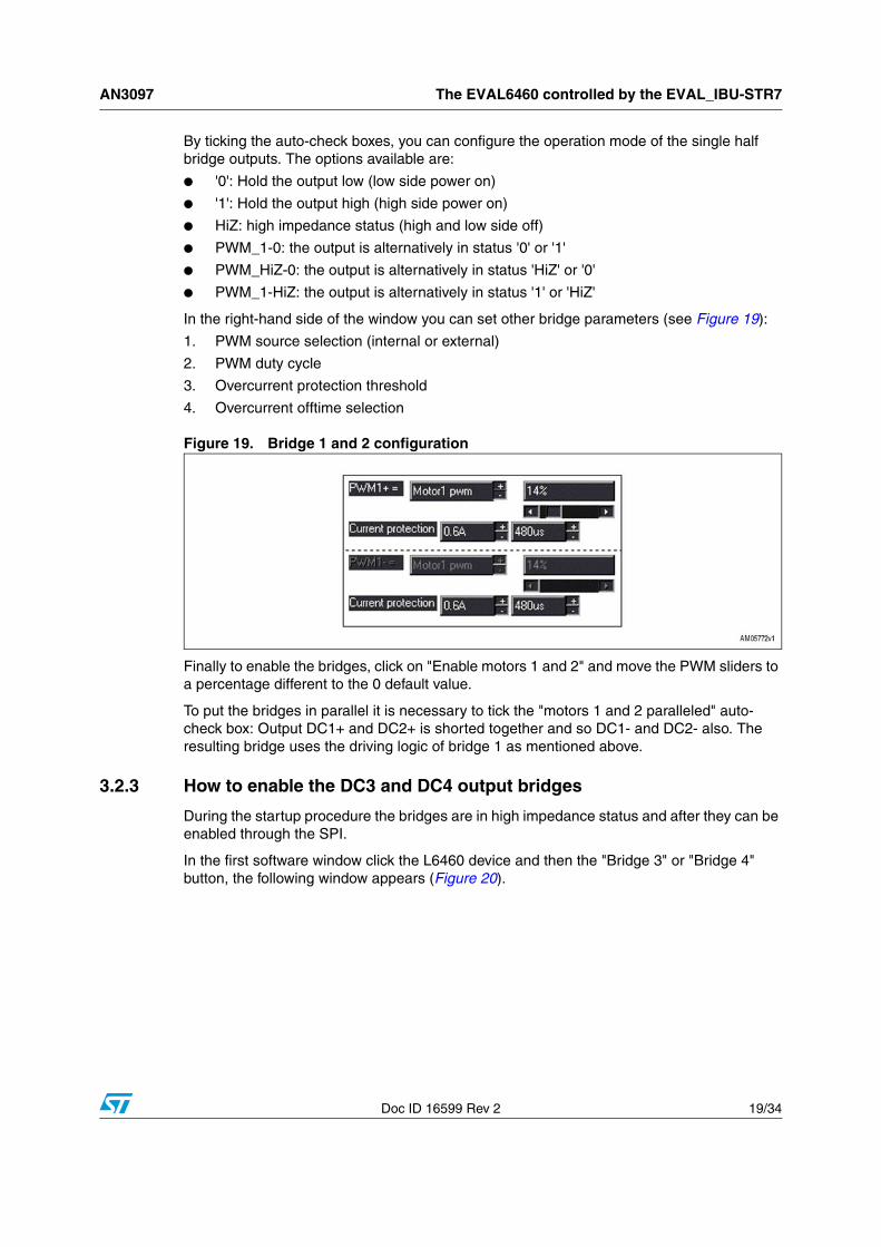
In the right-hand side of the window you can set other bridge parameters (see Figure 19):
1. PWM source selection (internal or external)
2. PWM duty cycle
3. Overcurrent protection threshold
4. Overcurrent offtime selection
Figure 19. Bridge 1 and 2 configuration
Finally to enable the bridges, click on "Enable motors 1 and 2" and move the PWM sliders to a percentage different to the 0 default value.
To put the bridges in parallel it is necessary to tick the "motors 1 and 2 paralleled" auto-check box: Output DC1+ and DC2+ is shorted together and so DC1- and DC2- also. The resulting bridge uses the driving logic of bridge 1 as mentioned above.
3.2.3 How to enable the DC3 and DC4 output bridges
During the startup procedure the bridges are in high impedance status and after they can be enabled through the SPI.
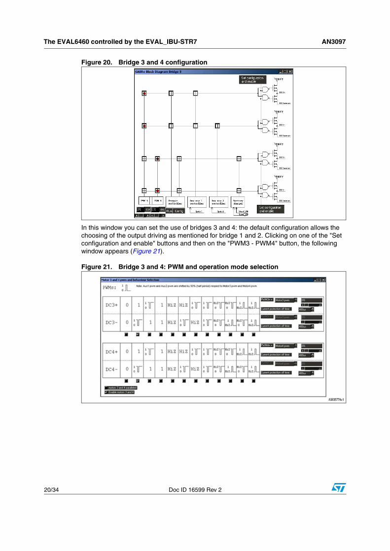
In the first software window click the L6460 device and then the "Bridge 3" or "Bridge 4" button, the following window appears (Figure 20).
The EVAL6460 controlled by the EVAL_IBU-STR7 AN3097
20/34 Doc ID 16599 Rev 2
Figure 20. Bridge 3 and 4 configuration
In this window you can set the use of bridges 3 and 4: the default configuration allows the choosing of the output driving as mentioned for bridge 1 and 2. Clicking on one of the "Set configuration and enable" buttons and then on the "PWM3 - PWM4" button, the following window appears (Figure 21).
Figure 21. Bridge 3 and 4: PWM and operation mode selection
AN3097 The EVAL6460 controlled by the EVAL_IBU-STR7
Doc ID 16599 Rev 2 21/34
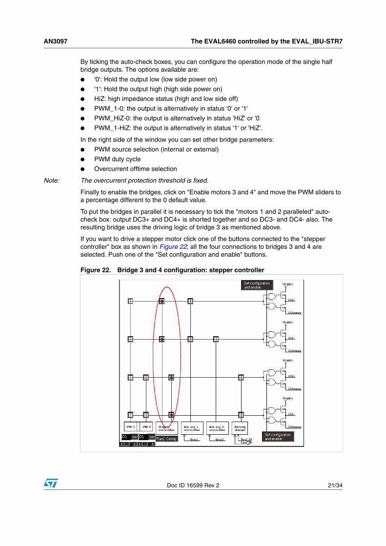
By ticking the auto-check boxes, you can configure the operation mode of the single half bridge outputs. The options available are:
● '0': Hold the output low (low side power on)
● '1': Hold the output high (high side power on)
● HiZ: high impedance status (high and low side off)
● PWM_1-0: the output is alternatively in status '0' or '1'
● PWM_HiZ-0: the output is alternatively in status 'HiZ' or '0
● PWM_1-HiZ: the output is alternatively in status '1' or 'HiZ'.
In the right side of the window you can set other bridge parameters:
● PWM source selection (internal or external)
● PWM duty cycle
● Overcurrent offtime selection
Note: The overcurrent protection threshold is fixed.
Finally to enable the bridges, click on "Enable motors 3 and 4" and move the PWM sliders to a percentage different to the 0 default value.
To put the bridges in parallel it is necessary to tick the "motors 1 and 2 paralleled" auto-check box: output DC3+ and DC4+ is shorted together and so DC3- and DC4- also. The resulting bridge uses the driving logic of bridge 3 as mentioned above.
If you want to drive a stepper motor click one of the buttons connected to the "stepper controller" box as shown in Figure 22; all the four connections to bridges 3 and 4 are selected. Push one of the "Set configuration and enable" buttons.
Figure 22. Bridge 3 and 4 configuration: stepper controller
The EVAL6460 controlled by the EVAL_IBU-STR7 AN3097
22/34 Doc ID 16599 Rev 2
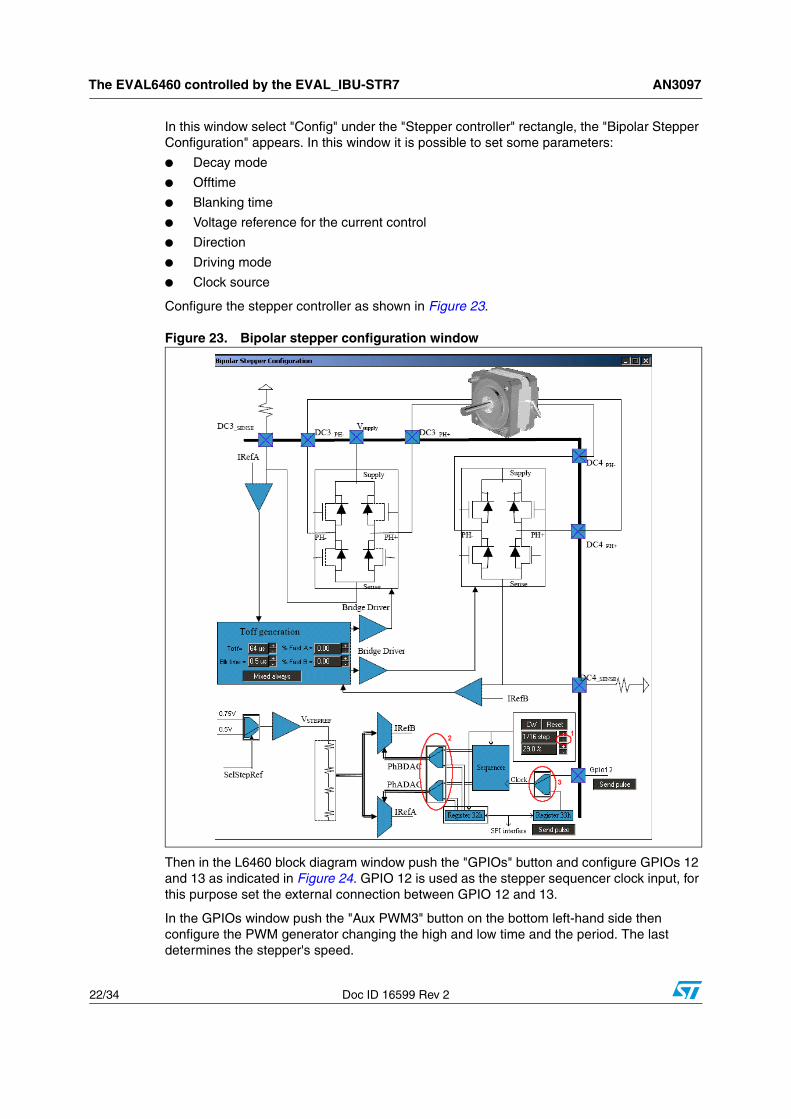
In this window select "Config" under the "Stepper controller" rectangle, the "Bipolar Stepper Configuration" appears. In this window it is possible to set some parameters:
● Decay mode
● Offtime
● Blanking time
● Voltage reference for the current control
● Direction
● Driving mode
● Clock source
Configure the stepper controller as shown in Figure 23.
Figure 23. Bipolar stepper configuration window
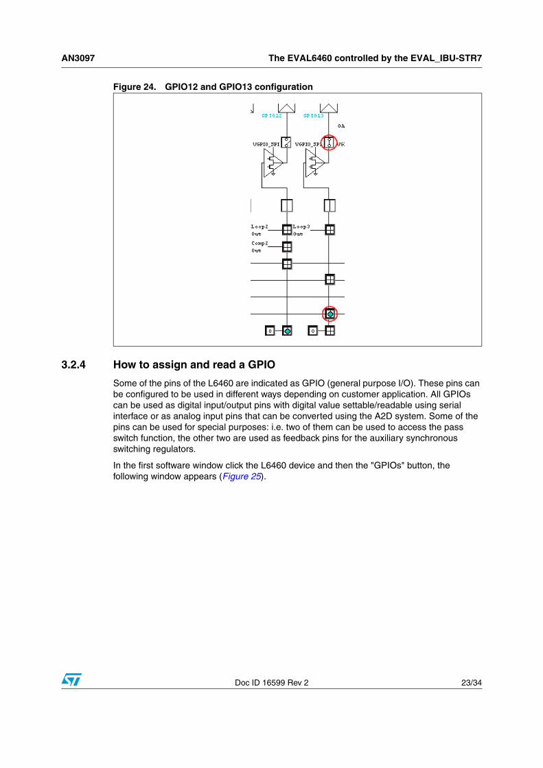
Then in the L6460 block diagram window push the "GPIOs" button and configure GPIOs 12 and 13 as indicated in Figure 24. GPIO 12 is used as the stepper sequencer clock input, for this purpose set the external connection between GPIO 12 and 13.
In the GPIOs window push the "Aux PWM3" button on the bottom left-hand side then configure the PWM generator changing the high and low time and the period. The last determines the stepper's speed.
AN3097 The EVAL6460 controlled by the EVAL_IBU-STR7
Doc ID 16599 Rev 2 23/34
Figure 24. GPIO12 and GPIO13 configuration
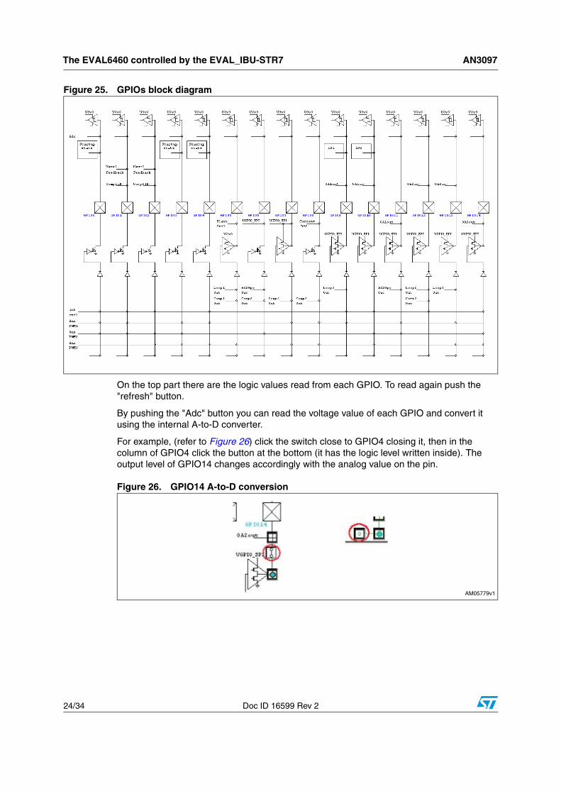
3.2.4 How to assign and read a GPIO
Some of the pins of the L6460 are indicated as GPIO (general purpose I/O). These pins can be configured to be used in different ways depending on customer application. All GPIOs can be used as digital input/output pins with digital value settable/readable using serial interface or as analog input pins that can be converted using the A2D system. Some of the pins can be used for special purposes: i.e. two of them can be used to access the pass switch function, the other two are used as feedback pins for the auxiliary synchronous switching regulators.
In the first software window click the L6460 device and then the "GPIOs" button, the following window appears (Figure 25).
The EVAL6460 controlled by the EVAL_IBU-STR7 AN3097
24/34 Doc ID 16599 Rev 2
Figure 25. GPIOs block diagram
On the top part there are the logic values read from each GPIO. To read again push the "refresh" button.
By pushing the "Adc" button you can read the voltage value of each GPIO and convert it using the internal A-to-D converter.
For example, (refer to Figure 26) click the switch close to GPIO4 closing it, then in the column of GPIO4 click the button at the bottom (it has the logic level written inside). The output level of GPIO14 changes accordingly with the analog value on the pin.
Figure 26. GPIO14 A-to-D conversion
AN3097 The EVAL6460 controlled by the EVAL_IBU-STR7
Doc ID 16599 Rev 2 25/34
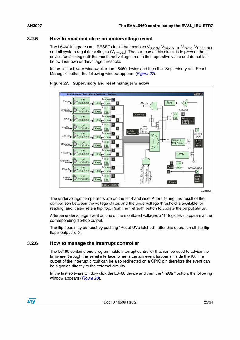
3.2.5 How to read and clear an undervoltage event
The L6460 integrates an nRESET circuit that monitors VSupply, VSupply_int, VPump, VGPIO_SPI and all system regulator voltages (VSystem). The purpose of this circuit is to prevent the device functioning until the monitored voltages reach their operative value and do not fall below their own undervoltage threshold.
In the first software window click the L6460 device and then the "Supervisory and Reset Manager" button, the following window appears (Figure 27).
Figure 27. Supervisory and reset manager window
The undervoltage comparators are on the left-hand side. After filtering, the result of the comparison between the voltage status and the undervoltage threshold is available for reading, and it also sets a flip-flop. Push the "refresh" button to update the output status.
After an undervoltage event on one of the monitored voltages a "1" logic level appears at the corresponding flip-flop output.
The flip-flops may be reset by pushing "Reset UVs latched", after this operation all the flip-flop's output is '0'.
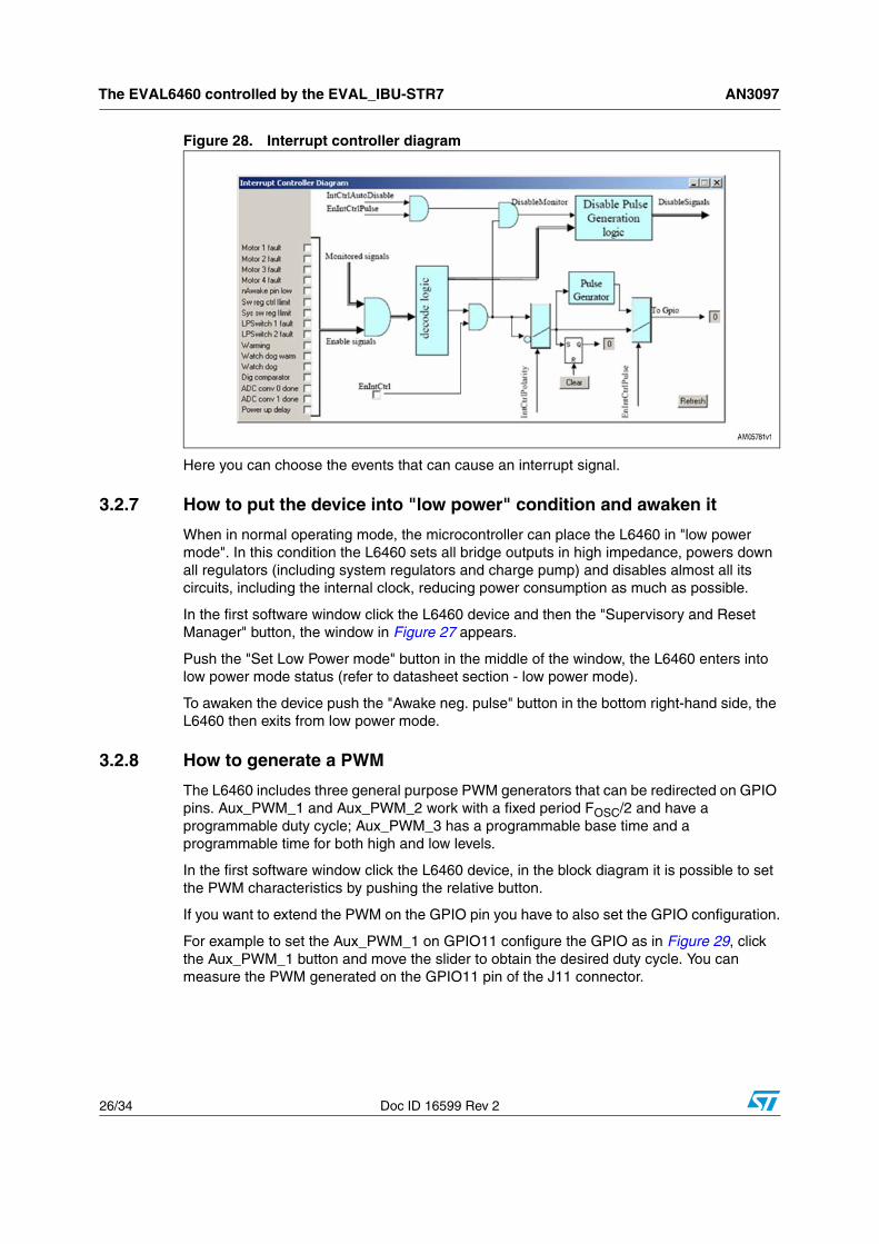
3.2.6 How to manage the interrupt controller
The L6460 contains one programmable interrupt controller that can be used to advise the firmware, through the serial interface, when a certain event happens inside the IC. The output of the interrupt circuit can be also redirected on a GPIO pin therefore the event can be signaled directly to the external circuits.
In the first software window click the L6460 device and then the "IntCtrl" button, the following window appears (Figure 28).
The EVAL6460 controlled by the EVAL_IBU-STR7 AN3097
26/34 Doc ID 16599 Rev 2
Figure 28. Interrupt controller diagram
Here you can choose the events that can cause an interrupt signal.
3.2.7 How to put the device into "low power" condition and awaken it
When in normal operating mode, the microcontroller can place the L6460 in "low power mode". In this condition the L6460 sets all bridge outputs in high impedance, powers down all regulators (including system regulators and charge pump) and disables almost all its circuits, including the internal clock, reducing power consumption as much as possible.
In the first software window click the L6460 device and then the "Supervisory and Reset Manager" button, the window in Figure 27 appears.
Push the "Set Low Power mode" button in the middle of the window, the L6460 enters into low power mode status (refer to datasheet section - low power mode).
To awaken the device push the "Awake neg. pulse" button in the bottom right-hand side, the L6460 then exits from low power mode.
3.2.8 How to generate a PWM
The L6460 includes three general purpose PWM generators that can be redirected on GPIO pins. Aux_PWM_1 and Aux_PWM_2 work with a fixed period FOSC/2 and have a programmable duty cycle; Aux_PWM_3 has a programmable base time and a programmable time for both high and low levels.
In the first software window click the L6460 device, in the block diagram it is possible to set the PWM characteristics by pushing the relative button.
If you want to extend the PWM on the GPIO pin you have to also set the GPIO configuration.
For example to set the Aux_PWM_1 on GPIO11 configure the GPIO as in Figure 29, click the Aux_PWM_1 button and move the slider to obtain the desired duty cycle. You can measure the PWM generated on the GPIO11 pin of the J11 connector.
AN3097 The EVAL6460 controlled by the EVAL_IBU-STR7
Doc ID 16599 Rev 2 27/34
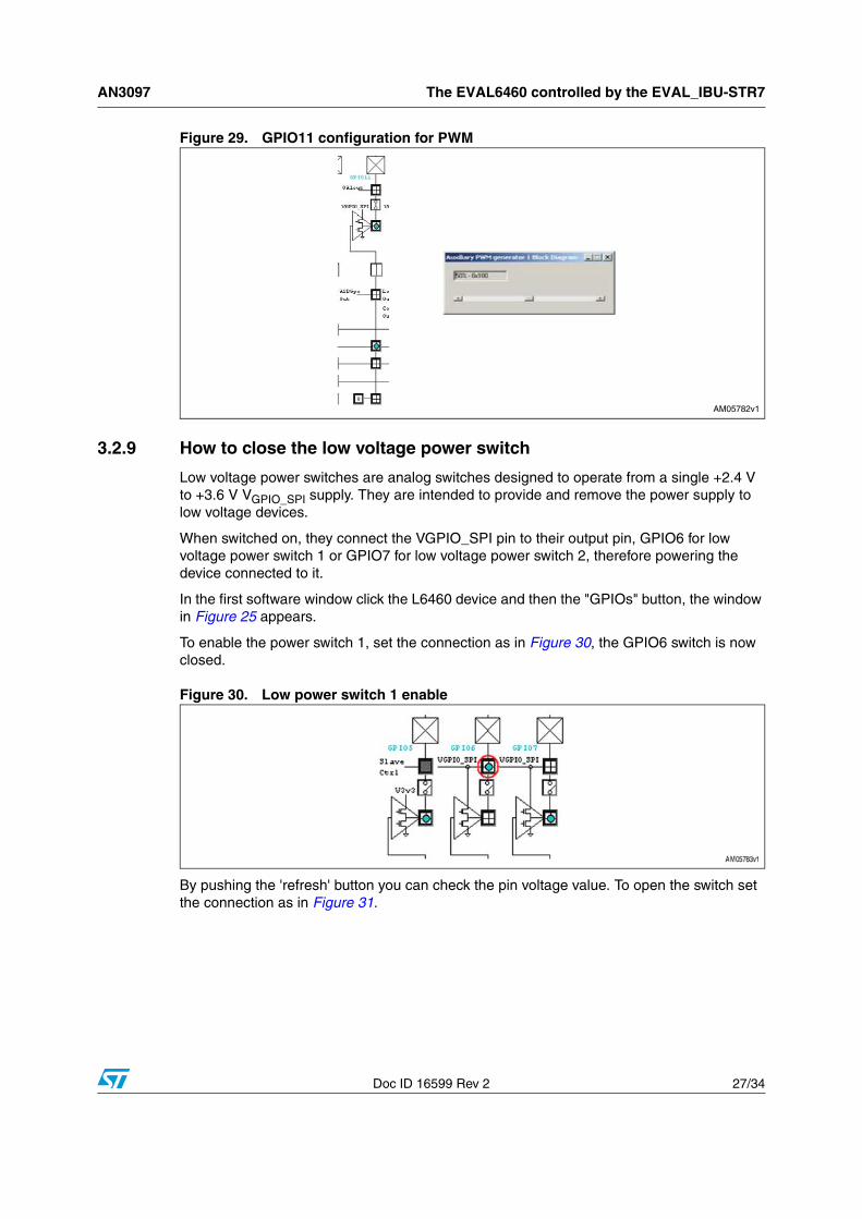
Figure 29. GPIO11 configuration for PWM
3.2.9 How to close the low voltage power switch
Low voltage power switches are analog switches designed to operate from a single +2.4 V to +3.6 V VGPIO_SPI supply. They are intended to provide and remove the power supply to low voltage devices.
When switched on, they connect the VGPIO_SPI pin to their output pin, GPIO6 for low voltage power switch 1 or GPIO7 for low voltage power switch 2, therefore powering the device connected to it.
In the first software window click the L6460 device and then the "GPIOs" button, the window in Figure 25 appears.
To enable the power switch 1, set the connection as in Figure 30, the GPIO6 switch is now closed.
Figure 30. Low power switch 1 enable
By pushing the 'refresh' button you can check the pin voltage value. To open the switch set the connection as in Figure 31.
The EVAL6460 controlled by the EVAL_IBU-STR7 AN3097
28/34 Doc ID 16599 Rev 2
Figure 31. Low power switch 1 disable
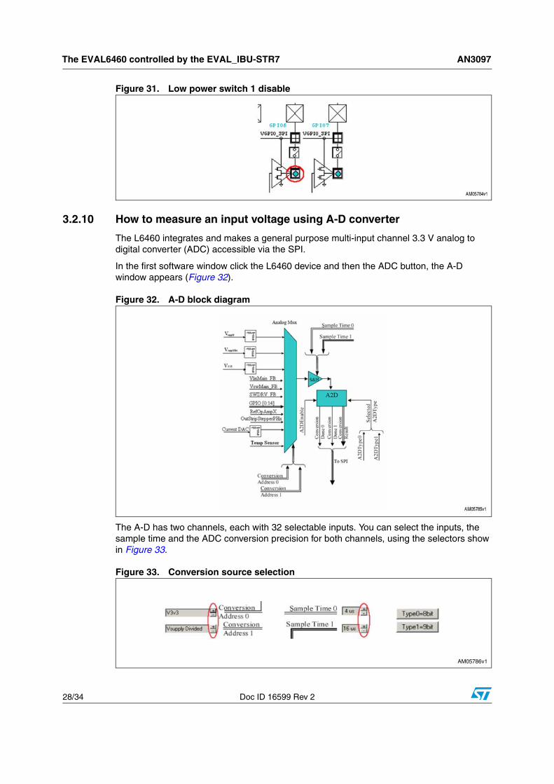
3.2.10 How to measure an input voltage using A-D converter
The L6460 integrates and makes a general purpose multi-input channel 3.3 V analog to digital converter (ADC) accessible via the SPI.
In the first software window click the L6460 device and then the ADC button, the A-D window appears (Figure 32).
Figure 32. A-D block diagram
The A-D has two channels, each with 32 selectable inputs. You can select the inputs, the sample time and the ADC conversion precision for both channels, using the selectors show in Figure 33.
Figure 33. Conversion source selection
AN3097 The EVAL6460 controlled by the EVAL_IBU-STR7
Doc ID 16599 Rev 2 29/34
To start the conversion push the "Start0" or "Start1" buttons, in the text box you can read the result register and the related voltage (the most significant bit of the result register is the "done" flag).
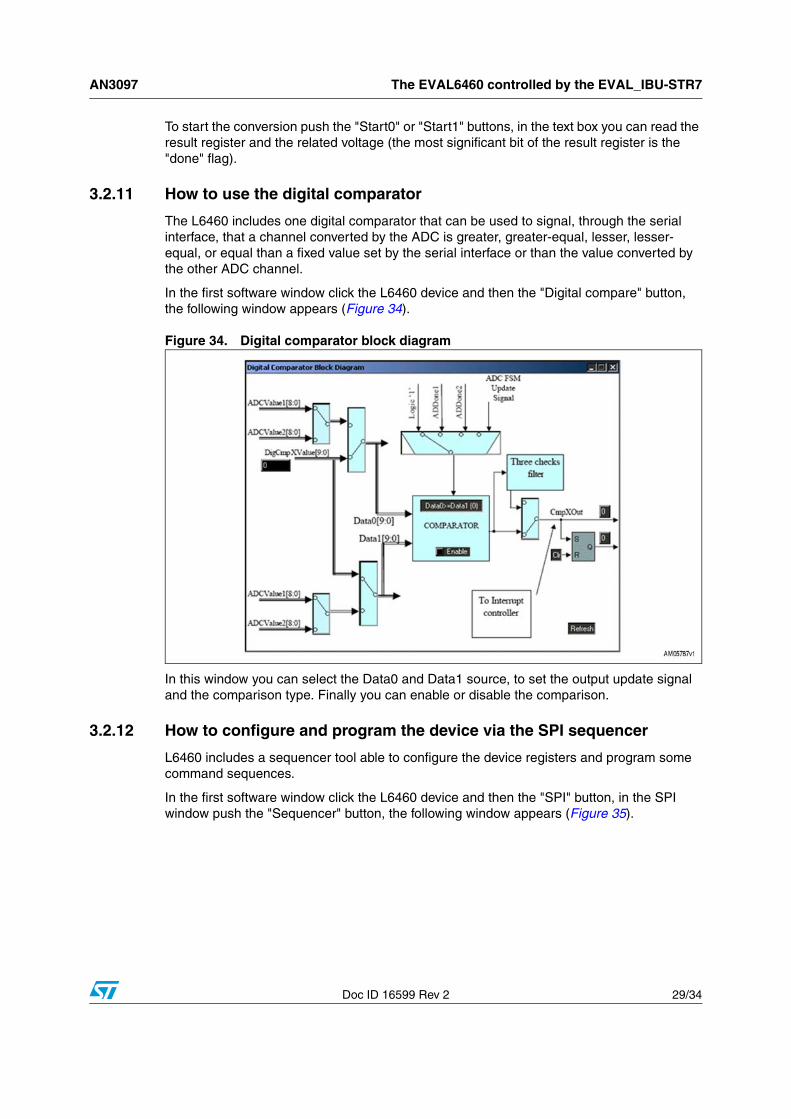
3.2.11 How to use the digital comparator
The L6460 includes one digital comparator that can be used to signal, through the serial interface, that a channel converted by the ADC is greater, greater-equal, lesser, lesser-equal, or equal than a fixed value set by the serial interface or than the value converted by the other ADC channel.
In the first software window click the L6460 device and then the "Digital compare" button, the following window appears (Figure 34).
Figure 34. Digital comparator block diagram
In this window you can select the Data0 and Data1 source, to set the output update signal and the comparison type. Finally you can enable or disable the comparison.
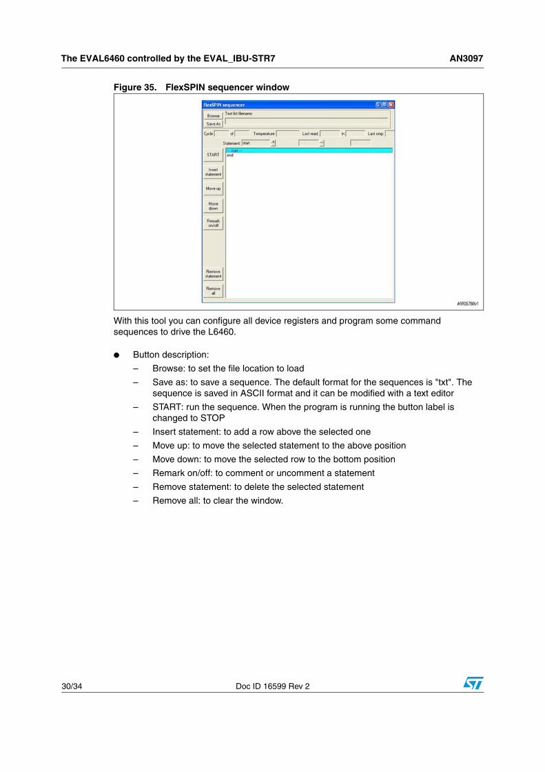
3.2.12 How to configure and program the device via the SPI sequencer
L6460 includes a sequencer tool able to configure the device registers and program some command sequences.
In the first software window click the L6460 device and then the "SPI" button, in the SPI window push the "Sequencer" button, the following window appears (Figure 35).
The EVAL6460 controlled by the EVAL_IBU-STR7 AN3097
30/34 Doc ID 16599 Rev 2
Figure 35. FlexSPIN sequencer window
With this tool you can configure all device registers and program some command sequences to drive the L6460.
● Button description:
– Browse: to set the file location to load
– Save as: to save a sequence. The default format for the sequences is "txt". The sequence is saved in ASCII format and it can be modified with a text editor
– START: run the sequence. When the program is running the button label is changed to STOP
– Insert statement: to add a row above the selected one
– Move up: to move the selected statement to the above position
– Move down: to move the selected row to the bottom position
– Remark on/off: to comment or uncomment a statement
– Remove statement: to delete the selected statement
– Remove all: to clear the window.
AN3097 The EVAL6460 controlled by the EVAL_IBU-STR7
Doc ID 16599 Rev 2 31/34
● To choose a statement use the + or - buttons near the "Statement" field. The instruction set is:
– Add/sub/mul/div: add/subtract/multiply/divide a variable and a constant, the result is put into the variable register
– Inc/dec: increment/decrement a variable of 1 unit
– Logicaland/or/exor: make the and/or/exor logical operation between a variable and a constant. The result is put into the variable register
– Compare: compare a variable with a constant. The result indicates that the variable is lesser, equal or greater than the constant
– Delay: stop the execution for a specified time expressed in milliseconds
– End: indicate the end of the program, it must be the last statement
– Label: assign a label to the statement (hex format)
– Goto: jump to the label indicated
– If: continue the execution starting from a label until the result of compare is the set one, otherwise jump to the successive statement
– Read: read the register value and assign it to a variable
– Readtemperature: read the device temperature using the integrates A-to-D. The value is displayed in the "Temperature" window
– Repeat: repeat the label for the indicated times
– Setdigio: no operation
– Stopprocedure: set the routine which is executed if the STOP button is pushed
– Write: write a constant in the indicated device register (hex format)
– Writevar: write a variable in the indicated device register (hex format)
Note: Each loop created with if, goto or repeat statement must include a delay statement, otherwise the program does not respond to the STOP command.
The execution time of a write or writevar instruction is about 6 ms, read about 9 ms and readtemperature about 35 ms. The other operations are faster and depend on the PC used.
The readtemperature instruction changes the A-to-D converter settings.
The numbers written in the window field are intended as hex values.
For more details on device registers refer to the L6460 user manual.
3.2.13 How to read the device temperature
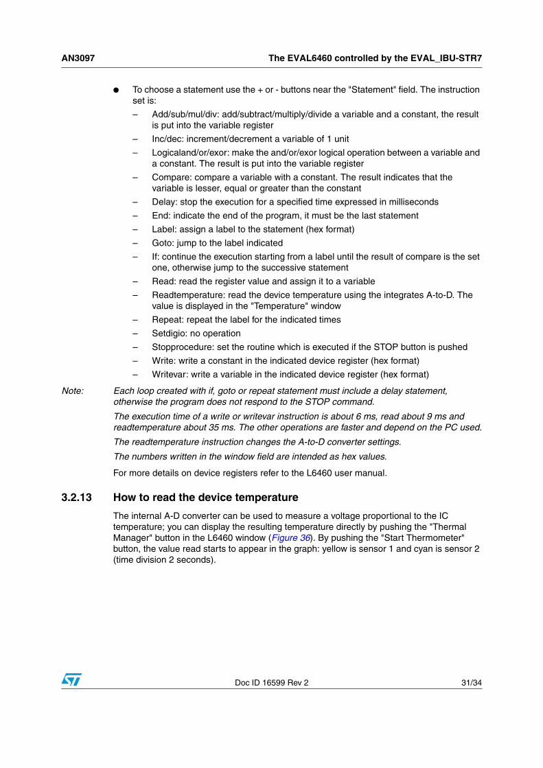
The internal A-D converter can be used to measure a voltage proportional to the IC temperature; you can display the resulting temperature directly by pushing the "Thermal Manager" button in the L6460 window (Figure 36). By pushing the "Start Thermometer" button, the value read starts to appear in the graph: yellow is sensor 1 and cyan is sensor 2 (time division 2 seconds).
The EVAL6460 controlled by the EVAL_IBU-STR7 AN3097
32/34 Doc ID 16599 Rev 2
Figure 36. Thermal manager window
3.2.14 How to work in master - slave configuration
1. Configure the slave board as described:
– JP1 in slave position
– Configuration jumpers: JP2 high, JP3 open, JP4 low
– Set the ID jumper: JP5 high and JP6 low
– Awake input: JP9 open
2. Connect the slave board to the master board using the 10 pin connectors (J1)
3. Connect loads and supplies
4. Run the software, click the L6460 device and then push the "SPI" button
5. Push "Sample ID" on the top left-hand side: the master board is accessed by writing "Msg address" equal 0 in this window, and the slave board with "Msg address" equal 1.
Note: The turn-on and turn-off operations must be done on master ("Msg address'"equal 0).
AN3097 Revision history
Doc ID 16599 Rev 2 33/34
4 Revision history
Table 4. Document revision history
Date Revision Changes
03-May-2010 1 Initial release
19-May-2010 2 Modified: Figure 1, 2, 3, 4, 7, 8, 9, 10, 11 and 12
AN3097
34/34 Doc ID 16599 Rev 2
Please Read Carefully:
Information in this document is provided solely in connection with ST products. STMicroelectronics NV and its subsidiaries (“ST”) reserve theright to make changes, corrections, modifications or improvements, to this document, and the products and services described herein at anytime, without notice.
All ST products are sold pursuant to ST’s terms and conditions of sale.
Purchasers are solely responsible for the choice, selection and use of the ST products and services described herein, and ST assumes noliability whatsoever relating to the choice, selection or use of the ST products and services described herein.
No license, express or implied, by estoppel or otherwise, to any intellectual property rights is granted under this document. If any part of thisdocument refers to any third party products or services it shall not be deemed a license grant by ST for the use of such third party productsor services, or any intellectual property contained therein or considered as a warranty covering the use in any manner whatsoever of suchthird party products or services or any intellectual property contained therein.
UNLESS OTHERWISE SET FORTH IN ST’S TERMS AND CONDITIONS OF SALE ST DISCLAIMS ANY EXPRESS OR IMPLIEDWARRANTY WITH RESPECT TO THE USE AND/OR SALE OF ST PRODUCTS INCLUDING WITHOUT LIMITATION IMPLIEDWARRANTIES OF MERCHANTABILITY, FITNESS FOR A PARTICULAR PURPOSE (AND THEIR EQUIVALENTS UNDER THE LAWSOF ANY JURISDICTION), OR INFRINGEMENT OF ANY PATENT, COPYRIGHT OR OTHER INTELLECTUAL PROPERTY RIGHT.
UNLESS EXPRESSLY APPROVED IN WRITING BY AN AUTHORIZED ST REPRESENTATIVE, ST PRODUCTS ARE NOTRECOMMENDED, AUTHORIZED OR WARRANTED FOR USE IN MILITARY, AIR CRAFT, SPACE, LIFE SAVING, OR LIFE SUSTAININGAPPLICATIONS, NOR IN PRODUCTS OR SYSTEMS WHERE FAILURE OR MALFUNCTION MAY RESULT IN PERSONAL INJURY,DEATH, OR SEVERE PROPERTY OR ENVIRONMENTAL DAMAGE. ST PRODUCTS WHICH ARE NOT SPECIFIED AS "AUTOMOTIVEGRADE" MAY ONLY BE USED IN AUTOMOTIVE APPLICATIONS AT USER’S OWN RISK.
Resale of ST products with provisions different from the statements and/or technical features set forth in this document shall immediately voidany warranty granted by ST for the ST product or service described herein and shall not create or extend in any manner whatsoever, anyliability of ST.
ST and the ST logo are trademarks or registered trademarks of ST in various countries.
Information in this document supersedes and replaces all information previously supplied.
The ST logo is a registered trademark of STMicroelectronics. All other names are the property of their respective owners.
© 2010 STMicroelectronics - All rights reserved
STMicroelectronics group of companies
Australia - Belgium - Brazil - Canada - China - Czech Republic - Finland - France - Germany - Hong Kong - India - Israel - Italy - Japan - Malaysia - Malta - Morocco - Philippines - Singapore - Spain - Sweden - Switzerland - United Kingdom - United States of America
www.st.com