Embed Size (px)
Citation preview
For further information contact your local STMicroelectronics sales office.
January 2013 Doc ID 024032 Rev 1 1/14
14
EVAL-RHF1201V2
EVAL-RHF1201V2 evaluation board
Data brief
Features
■ Mounted Engineering Model RHF1201K1: Rad-hard, 50 Msps, 12-bit analog-to-digital converter (see RHF1201 datasheet for further information)
■ Mounted components (ready-to-use)
■ Material: two-layered FR-4
■ PCB thickness: 1.6 mm
■ Copper thickness: 35 μm
■ Analog connections: SMA
■ Digital connections: IDC34
■ Supply connections: banana 2 mm
Description
This data brief describes the EVAL-RHF1201V2 evaluation board.
This evaluation board is a ready-to-use, configurable hardware which allows designers to efficiently test the RHF1201, a radiation-hardened, 12-bit, analog-to-digital converter.
This document shows the components incorporated on the EVAL-RHF1201V2 evaluation board and suggests several ways to use the board.
The EVAL-RHF1201V2 evaluation board is intended only for evaluation purposes.
www.st.com
Contents EVAL-RHF1201V2
2/14 Doc ID 024032 Rev 1
Contents
1 Bill of material . . . . . . . . . . . . . . . . . . . . . . . . . . . . . . . . . . . . . . . . . . . . . . 3
2 Device pin connections and description . . . . . . . . . . . . . . . . . . . . . . . . 4
3 Evaluation board schematic . . . . . . . . . . . . . . . . . . . . . . . . . . . . . . . . . . . 6
4 PCB print out . . . . . . . . . . . . . . . . . . . . . . . . . . . . . . . . . . . . . . . . . . . . . . . 7
5 Evaluation board description . . . . . . . . . . . . . . . . . . . . . . . . . . . . . . . . . . 9
5.1 Driving the analog input . . . . . . . . . . . . . . . . . . . . . . . . . . . . . . . . . . . . . . . 9
5.1.1 C5 capacitor (between VIN and VINB) . . . . . . . . . . . . . . . . . . . . . . . . . . 9
5.1.2 CR1, CR2 . . . . . . . . . . . . . . . . . . . . . . . . . . . . . . . . . . . . . . . . . . . . . . . . 9
5.1.3 Common mode voltage . . . . . . . . . . . . . . . . . . . . . . . . . . . . . . . . . . . . . 10
5.2 Input range . . . . . . . . . . . . . . . . . . . . . . . . . . . . . . . . . . . . . . . . . . . . . . . . 10
5.3 Polarization . . . . . . . . . . . . . . . . . . . . . . . . . . . . . . . . . . . . . . . . . . . . . . . . 10
5.4 Digital control pins . . . . . . . . . . . . . . . . . . . . . . . . . . . . . . . . . . . . . . . . . . .11
5.5 Driving the clock . . . . . . . . . . . . . . . . . . . . . . . . . . . . . . . . . . . . . . . . . . . . .11
5.6 Digital outputs . . . . . . . . . . . . . . . . . . . . . . . . . . . . . . . . . . . . . . . . . . . . . . 12
5.7 Supplies . . . . . . . . . . . . . . . . . . . . . . . . . . . . . . . . . . . . . . . . . . . . . . . . . . 12
5.8 Test points . . . . . . . . . . . . . . . . . . . . . . . . . . . . . . . . . . . . . . . . . . . . . . . . 12
6 Revision history . . . . . . . . . . . . . . . . . . . . . . . . . . . . . . . . . . . . . . . . . . . 13
EVAL-RHF1201V2 Bill of material
Doc ID 024032 Rev 1 3/14
1 Bill of material
Table 1. Bill of material
Used Part type(1) Designator Footprint Type
4 Red test point PT4, PT6, PT8, PT9
SIP1 Test point4 Black test point PT5, PT10, PT14, PT15
7 White test point PT1, PT2, PT3, PT7, PT11, PT12, PT13
1 4.7 μF C15 0603
Capacitor
3 10 nF C16, CR1, CR2
2 10 μF C11, C13 0805
2 22 μF C8, C9
9 470 nF C1, C2, C3, C4, C6, C7, C10, C12, C14 0603
1 100 pF C5 0402
4 10 μH L1, L2, L3, L4 1210 Inductor
3 0 Ω R3, R6, R26 0603
Resistor
16 33 Ω R10, R11, R12, R13, R14, R15, R16, R17, R18, R19, R20, R21, R22, R23, R24, R25
0402
3 50 Ω R1, R2, R9
0603 1 1 KΩ R8
2 100 KΩ R4, R5
4 Black banana 2 mm J5, J8, J10, J11
Connector 2 mm
Connector
4 Red banana 2 mm J6, J7, J9, J12
2 White banana 2 mm J1, J3
2 SMA right angle S1, S2 SMA
1 SMA straight S3
3 1 x 3 header MM JU4, JU5, JU6 SIP3
1 1 x 3 socket MF J4
1 1 x 2 header MM JU7 SIP2
1 2 x 17 header MM K1 IDC34
1 RHF1201 1 SO48 ceramic IC
1
NC
R7 0603
Resistor
1 C17 Capacitor
1 C18 0805
4 Jumper JU4, JU5, JU6, JU7 -
Jumper
1 200 KΩ J4 Potentiometer
1. MM = male-male, MF = male-female, and NC = not connected
Device pin connections and description EVAL-RHF1201V2
4/14 Doc ID 024032 Rev 1
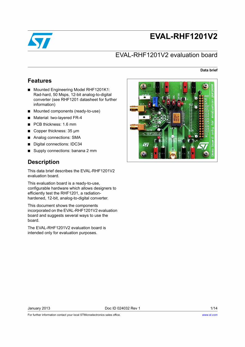
2 Device pin connections and description
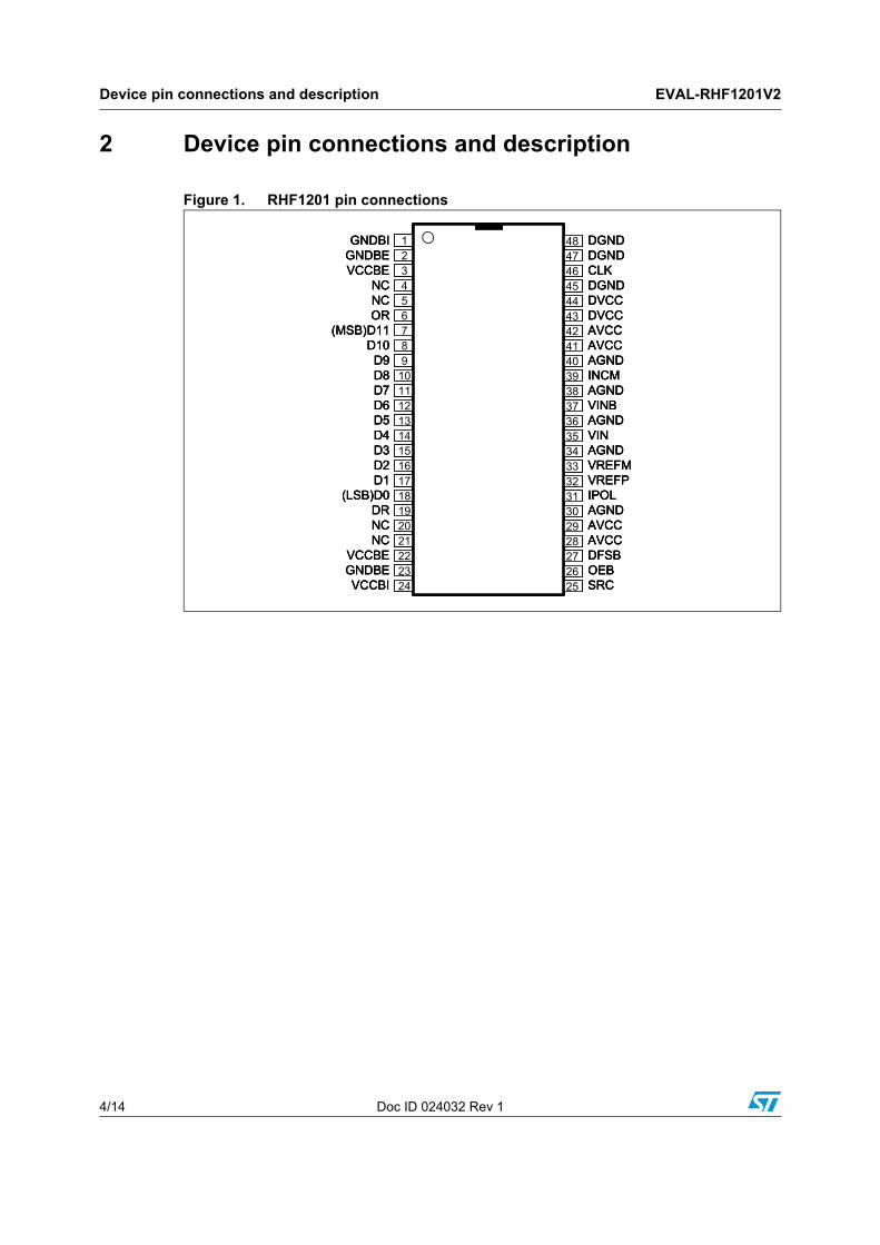
Figure 1. RHF1201 pin connections
GNDBIGNDBEVCCBE
NCNCOR
(MSB)D11D10
D9D8D7D6D5D4D3D2D1
(LSB)D0DRNCNC
VCCBEGNDBEVCCBI
DGNDDGNDCLKDGNDDVCCDVCCAVCCAVCCAGNDINCMAGNDVINBAGNDVINAGNDVREFMVREFPIPOLAGNDAVCCAVCCDFSBOEBSRC
123456789
101112131415161718192021222324
484746454443424140393837363534333231302928272625
GNDBIGNDBEVCCBE
NCNCOR
(MSB)D11D10
D9D8D7D6D5D4D3D2D1
(LSB)D0DRNCNC
VCCBEGNDBEVCCBI
DGNDDGNDCLKDGNDDVCCDVCCAVCCAVCCAGNDINCMAGNDVINBAGNDVINAGNDVREFMVREFPIPOLAGNDAVCCAVCCDFSBOEBSRC
123456789
101112131415161718192021222324
484746454443424140393837363534333231302928272625
GNDBIGNDBEVCCBE
NCNCOR
(MSB)D11D10
D9D8D7D6D5D4D3D2D1
(LSB)D0DRNCNC
VCCBEGNDBEVCCBI
DGNDDGNDCLKDGNDDVCCDVCCAVCCAVCCAGNDINCMAGNDVINBAGNDVINAGNDVREFMVREFPIPOLAGNDAVCCAVCCDFSBOEBSRC
123456789
101112131415161718192021222324
123456789
101112131415161718192021222324
484746454443424140393837363534333231302928272625
484746454443424140393837363534333231302928272625
EVAL-RHF1201V2 Device pin connections and description
Doc ID 024032 Rev 1 5/14
Table 2. RHF1201 pin description
Pin Name Description Observations Pin Name Description Observations
1 GNDBI Digital internal buffer GND 0 V
25 SRC Slew rate control
CMOS input (2.5 V/3.3 V)
2 GNDBE Digital external buffer GND 26 OEB Output enable bit
3 VCCBE Digital external buffer power supply
2.5 V/3.3 V 27 DFSB Data format select bit
4- NC Not connected
28 AVCC Analog power supply 2.5 V
5 29
6 OR Out of range
CMOS output (2.5 V/3.3 V)
30 AGND Analog ground 0 V
7 D11
(MSB) Most significant bit output 31 IPOL
Analog polarization current
8 D10
Digital output
32 VREFP Top voltage reference 1 V
9 D9 33 VREFM Bottom voltage reference 0 V
10 D8 34 AGND Analog ground
11 D7 35 VIN Analog input 1 Vpp
12 D6 36 AGND Analog ground 0 V
13 D5 37 VINB Inverted analog input 1 Vpp
14 D4 38 AGND Analog ground 0 V
15 D3 39 INCM Input common mode 0.5 V
16 D2 40 AGND Analog ground 0 V
17 D1 41
AVCC Analog power supply
2.5 V18
D0 (LSB)
42
19 DR 43 DVCC Digital power supply
20 - NC Not connected
44
21 45 DGND Digital ground 0 V
22 VCCBE Digital external buffer power supply
2.5 V/3.3 V 46 CLK Clock input CMOS input
2.5 V
23 GNDBE Digital external buffer GND 0 V 47
DGND Digital ground 0 V24 VCCBI
Digital internal buffer power supply
2.5 V 48
Evaluation board schematic EVAL-RHF1201V2
6/14 Doc ID 024032 Rev 1
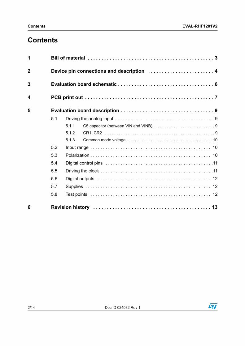
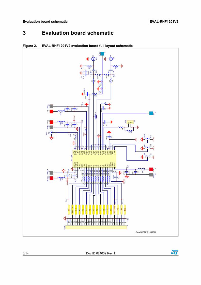
3 Evaluation board schematic
Figure 2. EVAL-RHF1201V2 evaluation board full layout schematic
EVAL-RHF1201V2 PCB print out
Doc ID 024032 Rev 1 7/14
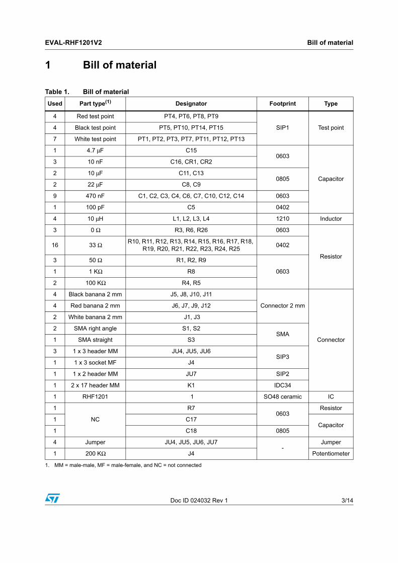
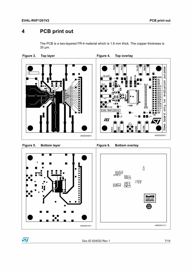
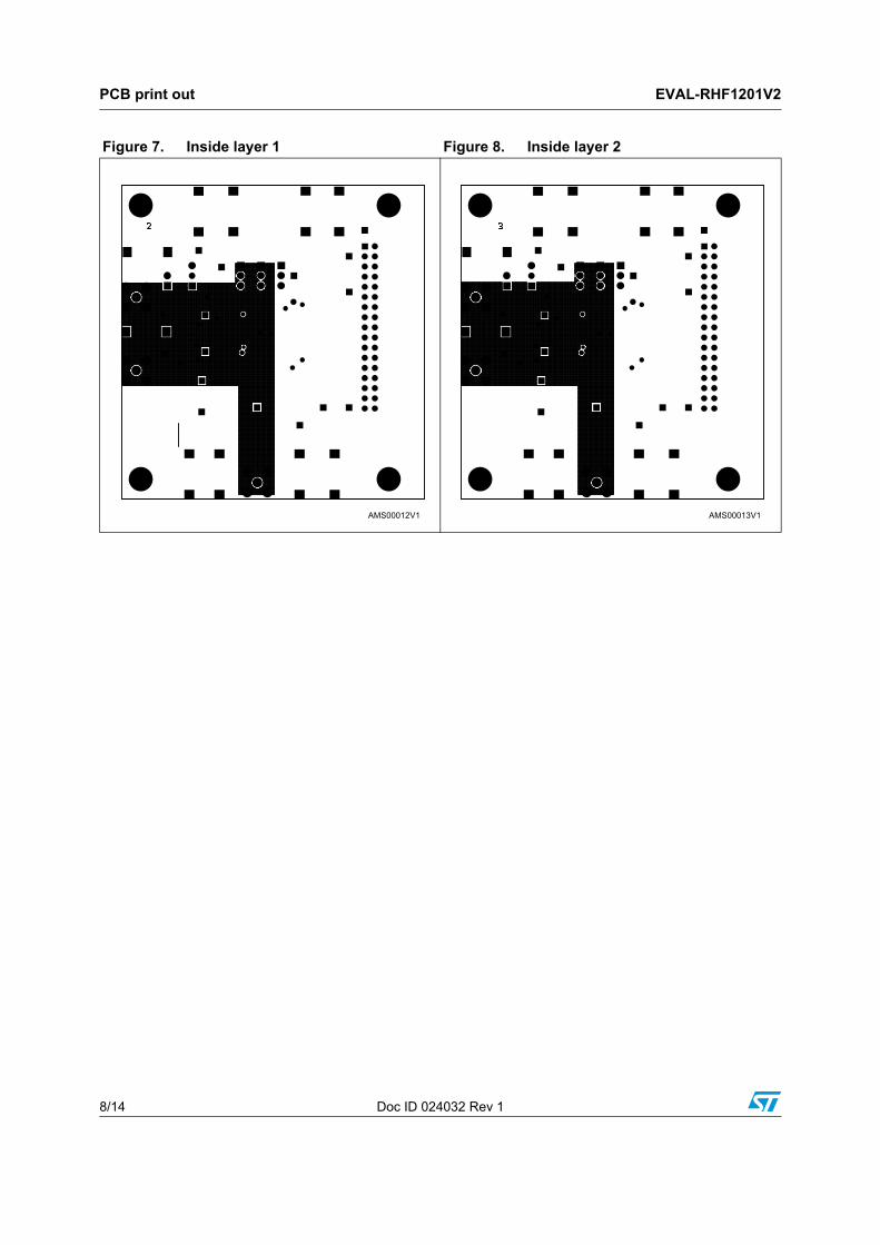
4 PCB print out
The PCB is a two-layered FR-4 material which is 1.6 mm thick. The copper thickness is 35 μm.
Figure 3. Top layer Figure 4. Top overlay
Figure 5. Bottom layer Figure 6. Bottom overlay
PCB print out EVAL-RHF1201V2
8/14 Doc ID 024032 Rev 1
Figure 7. Inside layer 1 Figure 8. Inside layer 2
EVAL-RHF1201V2 Evaluation board description
Doc ID 024032 Rev 1 9/14
5 Evaluation board description
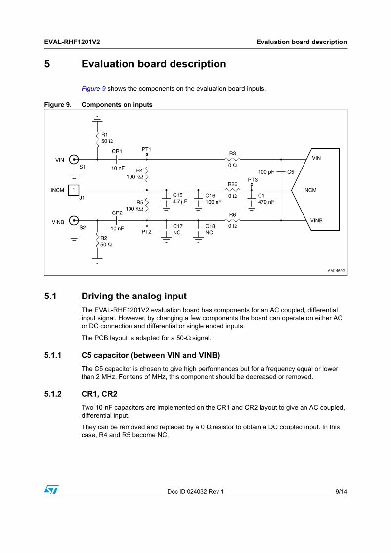
Figure 9 shows the components on the evaluation board inputs.
Figure 9. Components on inputs
5.1 Driving the analog input
The EVAL-RHF1201V2 evaluation board has components for an AC coupled, differential input signal. However, by changing a few components the board can operate on either AC or DC connection and differential or single ended inputs.
The PCB layout is adapted for a 50-Ω signal.
5.1.1 C5 capacitor (between VIN and VINB)
The C5 capacitor is chosen to give high performances but for a frequency equal or lower than 2 MHz. For tens of MHz, this component should be decreased or removed.
5.1.2 CR1, CR2
Two 10-nF capacitors are implemented on the CR1 and CR2 layout to give an AC coupled, differential input.
They can be removed and replaced by a 0 Ω resistor to obtain a DC coupled input. In this case, R4 and R5 become NC.
Evaluation board description EVAL-RHF1201V2
10/14 Doc ID 024032 Rev 1
5.1.3 Common mode voltage
The internal common mode voltage can be used or the voltage can be supplied externally by the connector J1.
5.2 Input range
The full scale range is twice the difference between VREFP and VREFM.
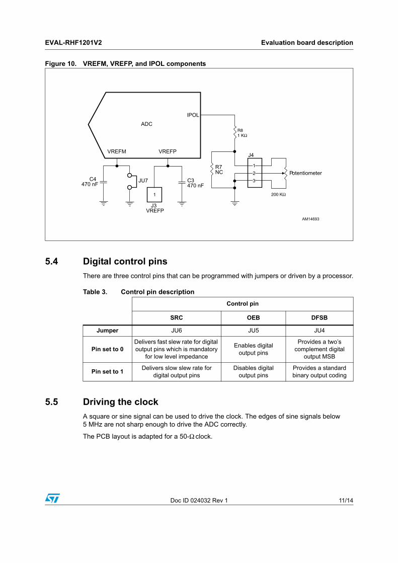
VREFM is connected to GND by the jumper JU7. It can easily be removed from GND and connected to a specified voltage, if needed, using JU7.
VREFP can be connected to an external voltage by the jumper J3 or it can be left at the default value (see RHF1201 datasheet).
VREFM is high impedance. VREFP is low impedance (about 39 Ω.).
The output code for differential inputs is as follows:
● Maximum output code is when: VIN – VINB = + (VREFP - VREFM)
● Half code is when: VIN = VINB
● Zero output code is when: VIN – VINB = - (VREFP - VREFM)
5.3 Polarization
To optimize analog consumption, the current on the IPOL pin (the IPOL pin delivers voltage) has to be adjusted. A resistor between this pin and GND fixes the current.
There is a 200 KΩ potentiometer on J4 to set this current at the right value for a given application.
If the user chooses a high value resistor for the potentiometer, the current is low (analog consumption is low) but a clock at high frequency must not be used.
The default potentiometer value is 12 KΩ for the 60 MHz clock.
See the RHF1201 datasheet to choose the resistor value which best fits your application.
EVAL-RHF1201V2 Evaluation board description
Doc ID 024032 Rev 1 11/14
Figure 10. VREFM, VREFP, and IPOL components
5.4 Digital control pins
There are three control pins that can be programmed with jumpers or driven by a processor.
5.5 Driving the clock
A square or sine signal can be used to drive the clock. The edges of sine signals below 5 MHz are not sharp enough to drive the ADC correctly.
The PCB layout is adapted for a 50-Ω clock.
Table 3. Control pin description
Control pin
SRC OEB DFSB
Jumper JU6 JU5 JU4
Pin set to 0Delivers fast slew rate for digital output pins which is mandatory
for low level impedance
Enables digital output pins
Provides a two’s complement digital
output MSB
Pin set to 1Delivers slow slew rate for
digital output pinsDisables digital
output pinsProvides a standard binary output coding
Evaluation board description EVAL-RHF1201V2
12/14 Doc ID 024032 Rev 1
5.6 Digital outputs
Digital output pins are sensitive to load. Consequently, there is no ground plane under the output lines to decrease parasitic capacitance on these pins.
There is also a 33 Ω resistor on each output line to decrease the capacitance recorded by the ADC.
5.7 Supplies
On each supply there is a 10 μH coil and two bypass capacitors. The capacitors are 470 nF and 10 μF or 22 μF.
5.8 Test points
There are 15 test points called TPx to help the user check signals on the board. Black points are grounds, reds points are supplies, and white points are signals.
EVAL-RHF1201V2 Revision history
Doc ID 024032 Rev 1 13/14
6 Revision history
Table 4. Document revision history
Date Revision Changes
28-Jan-2013 1 Initial release.
EVAL-RHF1201V2
14/14 Doc ID 024032 Rev 1
Please Read Carefully:
Information in this document is provided solely in connection with ST products. STMicroelectronics NV and its subsidiaries (“ST”) reserve the right to make changes, corrections, modifications or improvements, to this document, and the products and services described herein at any time, without notice.
All ST products are sold pursuant to ST’s terms and conditions of sale.
Purchasers are solely responsible for the choice, selection and use of the ST products and services described herein, and ST assumes no liability whatsoever relating to the choice, selection or use of the ST products and services described herein.
No license, express or implied, by estoppel or otherwise, to any intellectual property rights is granted under this document. If any part of this document refers to any third party products or services it shall not be deemed a license grant by ST for the use of such third party products or services, or any intellectual property contained therein or considered as a warranty covering the use in any manner whatsoever of such third party products or services or any intellectual property contained therein.
UNLESS OTHERWISE SET FORTH IN ST’S TERMS AND CONDITIONS OF SALE ST DISCLAIMS ANY EXPRESS OR IMPLIED WARRANTY WITH RESPECT TO THE USE AND/OR SALE OF ST PRODUCTS INCLUDING WITHOUT LIMITATION IMPLIED WARRANTIES OF MERCHANTABILITY, FITNESS FOR A PARTICULAR PURPOSE (AND THEIR EQUIVALENTS UNDER THE LAWS OF ANY JURISDICTION), OR INFRINGEMENT OF ANY PATENT, COPYRIGHT OR OTHER INTELLECTUAL PROPERTY RIGHT.
UNLESS EXPRESSLY APPROVED IN WRITING BY TWO AUTHORIZED ST REPRESENTATIVES, ST PRODUCTS ARE NOT RECOMMENDED, AUTHORIZED OR WARRANTED FOR USE IN MILITARY, AIR CRAFT, SPACE, LIFE SAVING, OR LIFE SUSTAINING APPLICATIONS, NOR IN PRODUCTS OR SYSTEMS WHERE FAILURE OR MALFUNCTION MAY RESULT IN PERSONAL INJURY, DEATH, OR SEVERE PROPERTY OR ENVIRONMENTAL DAMAGE. ST PRODUCTS WHICH ARE NOT SPECIFIED AS "AUTOMOTIVE GRADE" MAY ONLY BE USED IN AUTOMOTIVE APPLICATIONS AT USER’S OWN RISK.
Resale of ST products with provisions different from the statements and/or technical features set forth in this document shall immediately void any warranty granted by ST for the ST product or service described herein and shall not create or extend in any manner whatsoever, any liability of ST.
ST and the ST logo are trademarks or registered trademarks of ST in various countries.
Information in this document supersedes and replaces all information previously supplied.
The ST logo is a registered trademark of STMicroelectronics. All other names are the property of their respective owners.
© 2013 STMicroelectronics - All rights reserved
STMicroelectronics group of companies
Australia - Belgium - Brazil - Canada - China - Czech Republic - Finland - France - Germany - Hong Kong - India - Israel - Italy - Japan - Malaysia - Malta - Morocco - Philippines - Singapore - Spain - Sweden - Switzerland - United Kingdom - United States of America
www.st.com