Embed Size (px)
Citation preview
Oxford Semiconductor, Inc.1768 McCandless DriveMilpitas, CA 95035 USA
http://www.oxsemi.com
UG-0037 Nov 06
EV-TD122-UHC124-PCI and EV-TD122-UHC124
Evaluation BoardUser Guide
ii External—Free Release UG-0037 Nov 06
EV-TD122-UHC124-PCI and EV-TD122-UHC124 Evaluation Board User Guide Oxford Semiconductor, Inc.
© Oxford Semiconductor, Inc. 2006
The content of this manual is furnished for informational use only, is subject to change without notice, and should not be construed as a commitment by Oxford Semiconductor, Inc. Oxford Semiconductor, Inc. assumes no responsibility or liability for any errors or inaccuracies that may appear in this book.
ON Semiconductor is a register trademark of Semiconductor Components Industries, LLC.PLX is a registered trademark of PLX Technology.
All other trademarks are the property of their respective owners.
Contents
Preface ................................................................................................................ vRevision Information . . . . . . . . . . . . . . . . . . . . . . . . . . . . . . . . . . . . . . . . . . . . . vTypographic Conventions . . . . . . . . . . . . . . . . . . . . . . . . . . . . . . . . . . . . . . . . . vOrdering Information . . . . . . . . . . . . . . . . . . . . . . . . . . . . . . . . . . . . . . . . . . . . . vContacting Oxford Semiconductor . . . . . . . . . . . . . . . . . . . . . . . . . . . . . . . . . . vi
Chapter 1 - EV-TD122-UHC124-PCI ................................................................ 1-1Overview . . . . . . . . . . . . . . . . . . . . . . . . . . . . . . . . . . . . . . . . . . . . . . . . . . . . .1-1PCI Operation . . . . . . . . . . . . . . . . . . . . . . . . . . . . . . . . . . . . . . . . . . . . . . . . .1-2Configuration . . . . . . . . . . . . . . . . . . . . . . . . . . . . . . . . . . . . . . . . . . . . . . . . . .1-4Serial EEPROM Registers . . . . . . . . . . . . . . . . . . . . . . . . . . . . . . . . . . . . . . .1-4
Chapter 2 - EV-TD122-UHC124 Evaluation Board ........................................ 2-1Overview . . . . . . . . . . . . . . . . . . . . . . . . . . . . . . . . . . . . . . . . . . . . . . . . . . . . .2-1Board Operation Requirement . . . . . . . . . . . . . . . . . . . . . . . . . . . . . . . . . . . .2-2Default Configurations . . . . . . . . . . . . . . . . . . . . . . . . . . . . . . . . . . . . . . . . . .2-3Configurations . . . . . . . . . . . . . . . . . . . . . . . . . . . . . . . . . . . . . . . . . . . . . . . . .2-3Power Distribution . . . . . . . . . . . . . . . . . . . . . . . . . . . . . . . . . . . . . . . . . . . . . .2-3Reset . . . . . . . . . . . . . . . . . . . . . . . . . . . . . . . . . . . . . . . . . . . . . . . . . . . . . . . .2-4DP/DM Signals . . . . . . . . . . . . . . . . . . . . . . . . . . . . . . . . . . . . . . . . . . . . . . . . .2-4LEDs . . . . . . . . . . . . . . . . . . . . . . . . . . . . . . . . . . . . . . . . . . . . . . . . . . . . . . . .2-4Oscillator Input . . . . . . . . . . . . . . . . . . . . . . . . . . . . . . . . . . . . . . . . . . . . . . . .2-4Mounting Holes . . . . . . . . . . . . . . . . . . . . . . . . . . . . . . . . . . . . . . . . . . . . . . . .2-4Test Points . . . . . . . . . . . . . . . . . . . . . . . . . . . . . . . . . . . . . . . . . . . . . . . . . . .2-4
Chapter 3 - PCI104 Bridge Board ................................................................... 3-1Overview . . . . . . . . . . . . . . . . . . . . . . . . . . . . . . . . . . . . . . . . . . . . . . . . . . . . .3-1Power Distribution . . . . . . . . . . . . . . . . . . . . . . . . . . . . . . . . . . . . . . . . . . . . . .3-2Local Bus Configuration . . . . . . . . . . . . . . . . . . . . . . . . . . . . . . . . . . . . . . . . .3-3Local Bus Speed . . . . . . . . . . . . . . . . . . . . . . . . . . . . . . . . . . . . . . . . . . . . . . .3-3LEDs . . . . . . . . . . . . . . . . . . . . . . . . . . . . . . . . . . . . . . . . . . . . . . . . . . . . . . . .3-3Mounting Holes . . . . . . . . . . . . . . . . . . . . . . . . . . . . . . . . . . . . . . . . . . . . . . . .3-3
Chapter 4 - Schematics ................................................................................... 4-1Overview . . . . . . . . . . . . . . . . . . . . . . . . . . . . . . . . . . . . . . . . . . . . . . . . . . . . .4-1
UG-0037 Nov 06 External—Free Release iii
Contents EV-TD122-UHC124-PCI and EV-TD122-UHC124 Evaluation Board User Guide
This page is intentionally blank
iv External—Free Release UG-0037 Nov 06
Preface
This manual documents the EV‐TD122‐UHC124‐PCI Evaluation Board hardware.
Revision Information
Table I documents the revisions of this manual
Typographic Conventions
In this manual, the conventions listed in Table II apply.
Ordering Information
The following boards are available:
EV‐TD122‐UHC124‐PCI Evaluation Board with the TD122 (EV‐TD122‐UHC124‐PCI‐110)
EV‐TD122‐UHC124 Evaluation Board with the TD122 (EV‐TF122‐UHC124‐110)
EV‐TD122‐UHC124‐PCI Evaluation Board with the UHC124 (EV‐TD122‐UHC124‐PCI‐210)
EV‐TD122‐UHC124 Evaluation Board with the UHC124 (EV‐TF122‐UHC124‐210)
PCI104 Bridge Board (TDPCI104‐1000‐01)
Table I Revision Information
Revision ModificationNov 2006 First publication
Table II Typographic Conventions
Convention Meaning
Italic Letters With Initial Capital Letters A cross-reference to another publication
Courier Font Software code, or text typed in via a keyboard
1, 2, 3 A numbered list where the order of list items is significant
A list where the order of items is not significant
“Title” Cross-refers to another section within the document
Significant additional information
UG-0037 Nov 06 External—Free Release v
EV-TD122-UHC124-PCI and EV-TD122-UHC124 Evaluation Board User Guide
Contacting Oxford Semi-conductor
See the Oxford Semiconductor website (http://www.oxsemi.com) for further details about Oxford Semiconductor devices, or email [email protected].
vi External—Free Release UG-0037 Nov 06
Chapter 1
EV-TD122-UHC124-PCI
Overview The EV‐TD122‐UHC124‐PCI Evaluation Board is a system for TD122 and UHC124 customer evaluations and internal software development in the PC environment. The EV‐TD122‐UHC124‐PCI Evaluation Board allows the user to install and use the TD122 or UHC124 in any PCI‐based computer. Application software running on the system has access to the TD122 or UHC124 via the PCI memory space.The EV‐TD122‐UHC124 board can be used without the PCI Bridge Board, the PCI104.
The EV‐TD122‐UHC124‐PCI allows customers to:
Evaluate the Oxford Semiconductor TD122 and UHC124 USB host controller
Run TD122 and UHC124 demonstrations
Develop user software for TD122‐UHC124‐based applications
While the EV‐TD122‐UHC124‐PCI can be used to evaluate the TD122‐UHC124, it will not result in optimal performance due to the long access times of the PCI bus. For optimal performance evaluation, the TD122‐UHC124 should be placed directly on the system bus using the EV‐TD122‐UHC124 board as described in Chapter 2 .
The EV‐TD122‐UHC124‐PCI Evaluation Board is a two‐board combination of the following:
An EV‐TD122‐UHC124 Evaluation Board with 2 or 4 USB host ports
A 33 MHz, 32‐bit PCI Bridge Board, the PCI104
The EV‐TD122‐UHC124 Evaluation Board contains the TD122 or the UHC124 and all the USB‐specific hardware.
UG-0037 Nov 06 External—Free Release 1—1
EV-TD122-UHC124-PCI EV-TD122-UHC124-PCI and EV-TD122-UHC124 Evaluation Board User Guide
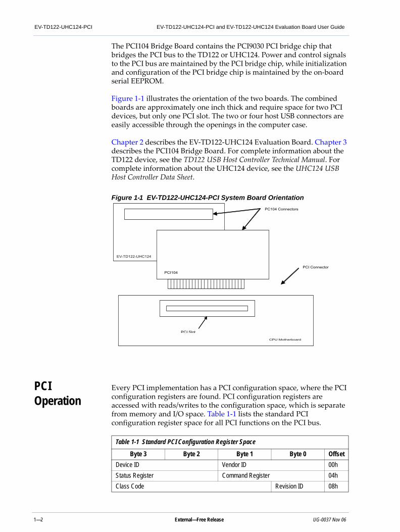
The PCI104 Bridge Board contains the PCI9030 PCI bridge chip that bridges the PCI bus to the TD122 or UHC124. Power and control signals to the PCI bus are maintained by the PCI bridge chip, while initialization and configuration of the PCI bridge chip is maintained by the on‐board serial EEPROM.
Figure 1‐1 illustrates the orientation of the two boards. The combined boards are approximately one inch thick and require space for two PCI devices, but only one PCI slot. The two or four host USB connectors are easily accessible through the openings in the computer case.
Chapter 2 describes the EV‐TD122‐UHC124 Evaluation Board. Chapter 3 describes the PCI104 Bridge Board. For complete information about the TD122 device, see the TD122 USB Host Controller Technical Manual. For complete information about the UHC124 device, see the UHC124 USB Host Controller Data Sheet.
Figure 1-1 EV-TD122-UHC124-PCI System Board Orientation
PCI Operation
Every PCI implementation has a PCI configuration space, where the PCI configuration registers are found. PCI configuration registers are accessed with reads/writes to the configuration space, which is separate from memory and I/O space. Table 1‐1 lists the standard PCI configuration register space for all PCI functions on the PCI bus.
PC104 Connectors
CPU Motherboard
PCI Slot
PCI ConnectorPCI104
EV-TD122-UHC124
Table 1-1 Standard PCI Configuration Register Space
Byte 3 Byte 2 Byte 1 Byte 0 OffsetDevice ID Vendor ID 00hStatus Register Command Register 04hClass Code Revision ID 08h
1—2 External—Free Release UG-0037 Nov 06
EV-TD122-UHC124-PCI and EV-TD122-UHC124 Evaluation Board User Guide EV-TD122-UHC124-PCI
The PCI104 can be identified on the PCI bus during enumeration by the following PCI configuration registers:
Most operating systems provide functions for finding devices on the PCI bus. These functions typically key off the Vendor and Device IDs, or the Class Code. Because the Class Code for the PCI104 appears as a PCI Bridge with sub class code “other”, the search should be keyed to the Vendor and Device IDs.
BIST Header Type Latency Timer Cache Line Size 0ChBase Address Register 0 (BAR 0) 10hBase Address Register 1 (BAR 1) 14hBase Address Register 2 (BAR 2) 18hBase Address Register 3 (BAR 3) 1ChBase Address Register 4 (BAR 4) 20hBase Address Register 5 (BAR 5) 24hCardBus CIS Pointer 28hSubsystem ID Subsystem Vendor ID 2ChExpansion ROM Base Address 30h
Reserved Capabilities Pointer
34h
Reserved 38hMax Latency Min Grant Interrupt Pin Interrupt Line 3Ch
Table 1-2 PCI Configuration Registers
Register Power-On ValueVendor ID 192EhDevice ID 012FhRevision 0001hClass Code 0680hSubsystem ID 012FhSubsystem Vendor ID 192Eh
Table 1-1 Standard PCI Configuration Register Space
Byte 3 Byte 2 Byte 1 Byte 0 Offset
UG-0037 Nov 06 External—Free Release 1—3
EV-TD122-UHC124-PCI EV-TD122-UHC124-PCI and EV-TD122-UHC124 Evaluation Board User Guide
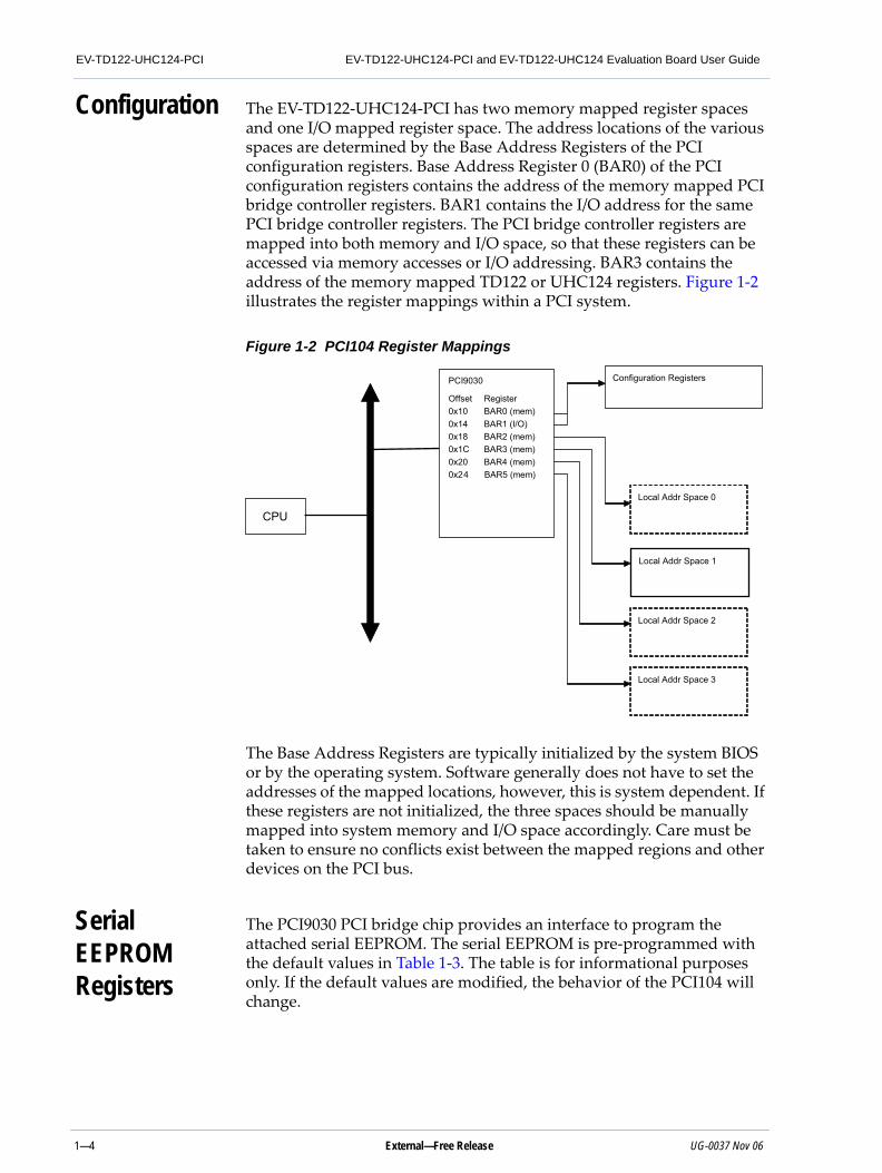
Configuration The EV‐TD122‐UHC124‐PCI has two memory mapped register spaces and one I/O mapped register space. The address locations of the various spaces are determined by the Base Address Registers of the PCI configuration registers. Base Address Register 0 (BAR0) of the PCI configuration registers contains the address of the memory mapped PCI bridge controller registers. BAR1 contains the I/O address for the same PCI bridge controller registers. The PCI bridge controller registers are mapped into both memory and I/O space, so that these registers can be accessed via memory accesses or I/O addressing. BAR3 contains the address of the memory mapped TD122 or UHC124 registers. Figure 1‐2 illustrates the register mappings within a PCI system.
Figure 1-2 PCI104 Register Mappings
The Base Address Registers are typically initialized by the system BIOS or by the operating system. Software generally does not have to set the addresses of the mapped locations, however, this is system dependent. If these registers are not initialized, the three spaces should be manually mapped into system memory and I/O space accordingly. Care must be taken to ensure no conflicts exist between the mapped regions and other devices on the PCI bus.
Serial EEPROM Registers
The PCI9030 PCI bridge chip provides an interface to program the attached serial EEPROM. The serial EEPROM is pre‐programmed with the default values in Table 1‐3. The table is for informational purposes only. If the default values are modified, the behavior of the PCI104 will change.
CPU
PCI9030
Offset 0x10 0x14 0x18 0x1C 0x20 0x24
Local Addr Space 0
Local Addr Space 1
Local Addr Space 2
Local Addr Space 3
Configuration Registers
Register BAR0 (mem) BAR1 (I/O) BAR2 (mem) BAR3 (mem) BAR4 (mem) BAR5 (mem)
1—4 External—Free Release UG-0037 Nov 06
EV-TD122-UHC124-PCI and EV-TD122-UHC124 Evaluation Board User Guide EV-TD122-UHC124-PCI
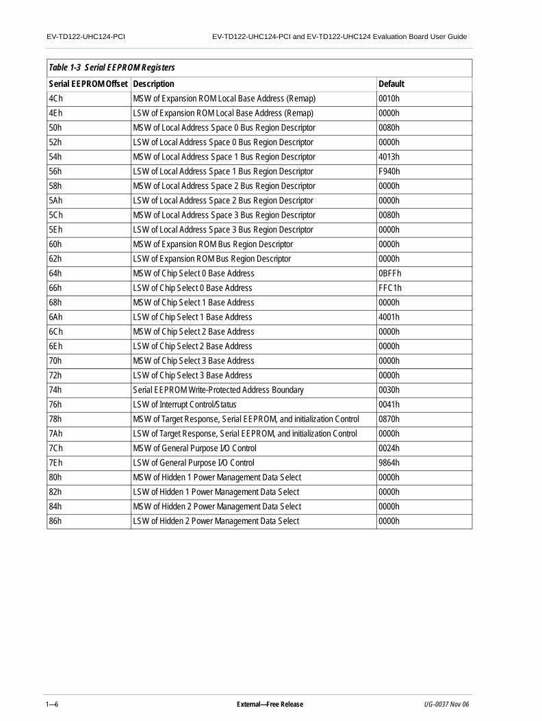
Table 1-3 Serial EEPROM Registers
Serial EEPROM Offset Description Default00h PCI Device ID 012Fh02h PCI Vendor ID 192Eh04h PCI Status Register 0290h06h PCI Command Register 0003h08h PCI Class Code 0680h0Ah PCI Class Code / Revision Number 0001h0Ch PCI Subsystem ID 016Bh0Eh PCI Subsystem Vendor ID 192Eh10h MSB New Capability Pointer 0000h12h LSB New Capability Pointer 0040h14h (Maximum Latency and Minimum Grant are not loadable) 0000h16h Interrupt Pin (Interrupt Line Routing is not loadable) 0100h18h MSW of Power Management Capabilities 4801h1Ah LSW of Power Management Next Capability Pointer /
Power Management Capability ID4801h
1Ch MSW of Power Management Data /PMCSR Bridge Support Extension 0000h1Eh LSW of Power Management Control/Status 0000h20h MSW of Hot Swap Control/Status 0000h22h LSW of Hot Swap Next Capability Pointer / Hot Swap Control 4C06h24h PCI Vital Product Data Address 0000h26h PCI Vital Product Data Next Capability Pointer /
PCI Vital Protocol Data Control0003h
28h MSW of Local Address Space 0 Range 0000h2Ah LSW of Local Address Space 0 Range 0000h2Ch MSW of Local Address Space 1 Range FFFFh2Eh LSW of Local Address Space 1 Range F000h30h MSW of Local Address Space 2 Range 0000h32h LSW of Local Address Space 2 Range 0000h34h MSW of Local Address Space 3 Range 0000h36h LSW of Local Address Space 3 Range 0000h38h MSW of Expansion ROM Range 0000h3Ah LSW of Expansion ROM Range 0000h3Ch MSW of Local Address Space 0 Local Base Address (Remap) 0000h3Eh LSW of Local Address Space 0 Local Base Address (Remap) 0000h40h MSW of Local Address Space 1 Local Base Address (Remap) 0000h42h LSW of Local Address Space 1 Local Base Address (Remap) 0001h44h MSW of Local Address Space 2 Local Base Address (Remap) 0000h46h LSW of Local Address Space 2 Local Base Address (Remap) 0000h48h MSW of Local Address Space 3 Local Base Address (Remap) 0000h4Ah LSW of Local Address Space 3 Local Base Address (Remap) 0000h
UG-0037 Nov 06 External—Free Release 1—5
EV-TD122-UHC124-PCI EV-TD122-UHC124-PCI and EV-TD122-UHC124 Evaluation Board User Guide
4Ch MSW of Expansion ROM Local Base Address (Remap) 0010h4Eh LSW of Expansion ROM Local Base Address (Remap) 0000h50h MSW of Local Address Space 0 Bus Region Descriptor 0080h52h LSW of Local Address Space 0 Bus Region Descriptor 0000h54h MSW of Local Address Space 1 Bus Region Descriptor 4013h56h LSW of Local Address Space 1 Bus Region Descriptor F940h58h MSW of Local Address Space 2 Bus Region Descriptor 0000h5Ah LSW of Local Address Space 2 Bus Region Descriptor 0000h5Ch MSW of Local Address Space 3 Bus Region Descriptor 0080h5Eh LSW of Local Address Space 3 Bus Region Descriptor 0000h60h MSW of Expansion ROM Bus Region Descriptor 0000h62h LSW of Expansion ROM Bus Region Descriptor 0000h64h MSW of Chip Select 0 Base Address 0BFFh66h LSW of Chip Select 0 Base Address FFC1h68h MSW of Chip Select 1 Base Address 0000h6Ah LSW of Chip Select 1 Base Address 4001h6Ch MSW of Chip Select 2 Base Address 0000h6Eh LSW of Chip Select 2 Base Address 0000h70h MSW of Chip Select 3 Base Address 0000h72h LSW of Chip Select 3 Base Address 0000h74h Serial EEPROM Write-Protected Address Boundary 0030h76h LSW of Interrupt Control/Status 0041h78h MSW of Target Response, Serial EEPROM, and initialization Control 0870h7Ah LSW of Target Response, Serial EEPROM, and initialization Control 0000h7Ch MSW of General Purpose I/O Control 0024h7Eh LSW of General Purpose I/O Control 9864h80h MSW of Hidden 1 Power Management Data Select 0000h82h LSW of Hidden 1 Power Management Data Select 0000h84h MSW of Hidden 2 Power Management Data Select 0000h86h LSW of Hidden 2 Power Management Data Select 0000h
Table 1-3 Serial EEPROM Registers
Serial EEPROM Offset Description Default
1—6 External—Free Release UG-0037 Nov 06
Chapter 2
EV-TD122-UHC124 Evaluation Board
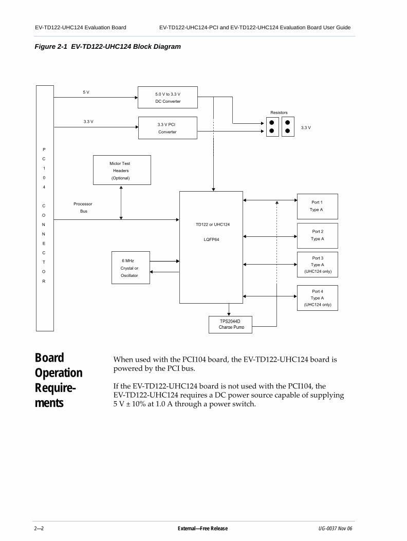
Overview This chapter describes the hardware operation and configuration options available for the EV‐TD122‐UHC124 in stand‐alone mode. These options allow customers to directly connect the TD122 or the UHC124 to their embedded processor or CPU without going through a PCI bus. The use of this board without the PCI bridge card increases performance and allows driver development in real‐world applications of the product. Figure 2‐1 shows the EV‐TD122‐UHC124 block diagram.
UG-0037 Nov 06 External—Free Release 2—1
EV-TD122-UHC124 Evaluation Board EV-TD122-UHC124-PCI and EV-TD122-UHC124 Evaluation Board User Guide
Figure 2-1 EV-TD122-UHC124 Block Diagram
Board Operation Require-ments
When used with the PCI104 board, the EV‐TD122‐UHC124 board is powered by the PCI bus.
If the EV‐TD122‐UHC124 board is not used with the PCI104, the EV‐TD122‐UHC124 requires a DC power source capable of supplying 5 V ± 10% at 1.0 A through a power switch.
5.0 V to 3.3 V
DC Converter
3.3 V
P
C
1
0
4
C
O
N
N
E
C
T
O
R
5 V
Mictor Test
Headers
(Optional)
3.3 V PCI
Converter
Resistors
Port 1
Type A
Port 3 Type A
Processor
Bus
TD122 or UHC124
LQFP64
6 MHz
Crystal or
Oscillator
TPS2044DCharge Pump
Port 2
Type A
3.3 V
(UHC124 only)
Port 4 Type A
(UHC124 only)
2—2 External—Free Release UG-0037 Nov 06
EV-TD122-UHC124-PCI and EV-TD122-UHC124 Evaluation Board User Guide EV-TD122-UHC124 Evaluation Board
Default Configura-tions
The following factory default settings support the development of the TD122 USB host for Port 1 and Port 2:
R54, R55 (0_1206 Ω) populated to route 5 V from the PCI104 connectors
R49 (0_1206 Ω) populated for 3.3 V from the voltage regulator
R23, R29, R31, R33 (0 Ω) populated for non‐multiplex mode (MODE = 1)
R26 (4.7 kΩ) populated for non‐multiplex mode (MODE = 1)
R38 (0 Ω) populated for /ADS signal inversion
R5, R9 (4.7 kΩ) populated when the TD122 is installed
R35, R52, R14, R41 (4.7 kΩ) populated for control signals pull‐ups
U1, U3, U5, U7 (with an STF201‐30) populated for ESD protection, series resistance, and pull‐downs to match impedance
Optional Configura-tions
If the UHC124 is installed in U10, R6 and R8 (4.7 kΩ) are installed as pull‐ups. This allows all four standard‐A ports to be used.
To use the EV‐TD122‐UHC124 in multiplex mode (MODE = 0):
1. Install a 0 Ω resistor in R24, R28, R32, R34.2. Remove the 0 Ω resistor from R23, R29, R31, R33.3. Install R27 (4.7 kΩ) and remove R26.
If the ADS input signal is already active high and does not need to be inverted, install R36 (0 Ω) and remove R38.
To use 3.3 V from the PCI connector, install R47 (0_1206 Ω) and remove R49.
To use a different ESD protection part, USBDF01W5, install U2, U4, U6, U8 (USBDF01W5) and remove U1, U3, U5, U7 (STF210‐30). Semtech STF201‐30 has DP/DM/VBUS ESD protection with 30 Ω series resistance and 15 kΩ pull‐down. ST Micro USBDF01W5 has DP/DM ESD protection with 33 Ω series resistance and 15 kΩ pull‐down.
Power Distribution
5 V Power Supply
The EV‐TD122‐UHC124 5 V power is supplied by one of two sources. The source is resistor selectable:
1. From the PC104 connector, by installing R54 and R55 (0 Ω) near the PC104 connector (default setting).
2. From an external power supply connected to JP9.3. Protection cir‐cuitry is not provided (remove R54 and R55).
UG-0037 Nov 06 External—Free Release 2—3
EV-TD122-UHC124 Evaluation Board EV-TD122-UHC124-PCI and EV-TD122-UHC124 Evaluation Board User Guide
3.3 V Power Supply
The EV‐TD122‐UHC124 3.3 V power is supplied by one of three sources:
1. From U12, a 5 V‐to‐3.3 V DC converter (default setting).2. From the PC104 connector. Install R47 (0_1206 Ω) and remove
R49.3. From an external power supply connected to the test pin on JP7.3.
Protection circuitry is not provided (remove R47 and R49).
Reset The /RESET pin of the TD122 or UHC124 is connected to the PC104 connector. Users can control /RESET through a CPU GPIO.
DP/DM Signals
Each of the DP/DM pairs has a 2‐pin, 0.1 inch spacing, connector to support attachment of a differential probe (JP1‐JP4)
These traces are impedance controlled to 90 Ω + 10%
LEDs The EV‐TD122‐UHC124 has the following LEDs to enable monitoring of the normal operation of the board:
D1‐D4: Type A VBUS Power Indicator
D5: 3.3 V Power Rail Indicator
D6: 5 V Power Rail Indicator
Oscillator Input
Use of a 6 MHz crystal, instead of a crystal oscillator, is recommended to lower EMI. The only footprint provided in the EV‐TD122‐UHC124 board uses a 6 MHz crystal located at Y1 (Ecliptek Corp., E2SAA18‐6.000M, 18 pF internal load).
Mounting Holes
The EV‐TD122‐UHC124 board has four un‐plated standoff holes, one near each corner of the board. Each hole is 0.146 inch in diameter. The placement matches the PCI104 PCI board which together make the EV‐TD122‐UHC124‐PCI.
Test Points The following test points are furnished on the EV‐TD122‐UHC124:
Ground Test Points JP5, JP6, JP8, and JP10
Power Test Points TP1‐TP4, TP5
2—4 External—Free Release UG-0037 Nov 06

Chapter 3
PCI104 Bridge Board
Overview The PCI104 contains a PLX Technology PCI9030 bridge chip, an Atmel AT93C66A‐10PI‐2.7, a ROM socket, and three connectors.
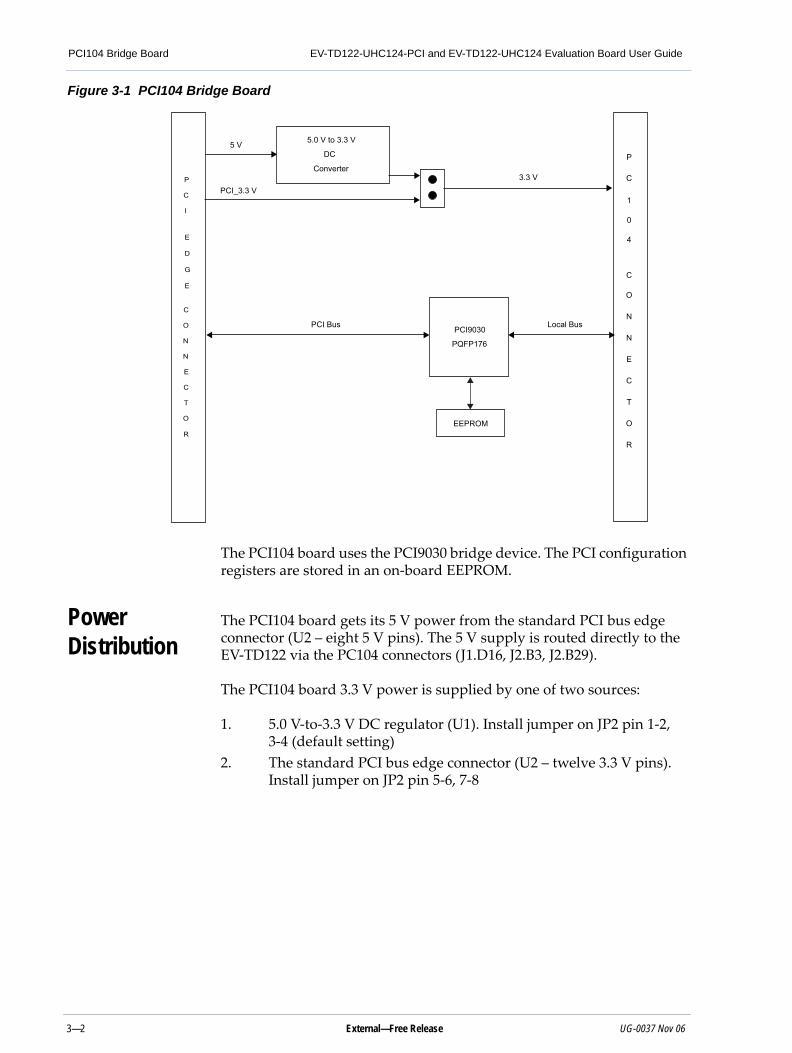
The PCI104 board bridges between the PCI bus and the TD122‐UHC124 local bus. The local bus is routed out to the standard PC104 connectors (J1 and J2). The EV‐TD122‐UHC124 interfaces to the PCI104 Bridge Card via these three female connectors. Another proprietary, non‐PC104 connector (J3) was added to support a 32‐bit interface and additional signals not included in the PC104 signal definition. Figure 3‐1 shows the PCI104 block diagram.
UG-0037 Nov 06 External—Free Release 3—1
PCI104 Bridge Board EV-TD122-UHC124-PCI and EV-TD122-UHC124 Evaluation Board User Guide
Figure 3-1 PCI104 Bridge Board
The PCI104 board uses the PCI9030 bridge device. The PCI configuration registers are stored in an on‐board EEPROM.
Power Distribution
The PCI104 board gets its 5 V power from the standard PCI bus edge connector (U2 – eight 5 V pins). The 5 V supply is routed directly to the EV‐TD122 via the PC104 connectors (J1.D16, J2.B3, J2.B29).
The PCI104 board 3.3 V power is supplied by one of two sources:
1. 5.0 V‐to‐3.3 V DC regulator (U1). Install jumper on JP2 pin 1‐2, 3‐4 (default setting)
2. The standard PCI bus edge connector (U2 – twelve 3.3 V pins). Install jumper on JP2 pin 5‐6, 7‐8
P
C
I
E
D
G
E
C
O
N
N
E
C
T
O
R
5.0 V to 3.3 V
DC
Converter
PCI9030
PQFP176
PCI_3.3 V
EEPROM
PCI Bus
Local Bus
5 V
3.3 V
P
C
O
N
N
E
C
T
O
R
1
0
4
C
3—2 External—Free Release UG-0037 Nov 06
EV-TD122-UHC124-PCI and EV-TD122-UHC124 Evaluation Board User Guide PCI104 Bridge Board
Local Bus Configuration
The PCI9030 local bus is connected directly to the EV‐TD122‐UHC124 board via the PC104 connectors. Refer to the PCI9030 Data Book for a detailed explanation of its operation.
PCI9030 CS1L chip select is routed to the EV‐TD122‐UHC124. Register Space 1 of the PCI9030 controls CS1L. The number values programmed into Space 1 registers of the EEPROM are shown below. Changing values in the EEPROM requires an application from PLX operating across the PCI bus. Space 1 has 8‐bit local and PCI space and contains 4 Kb memory space size. There is no prefetch on space 1.
Space 1 Range 0xFFFF_F000
Space 1 Remap 0x0000_0001
Space 1 Descriptor 0x4013_F940
Space 1 Base Address 0x0000_0801
Space 1 Initialization Control 0x0030_0041
The local timing is five WAIT states for READs (address‐to‐data) and seven for WRITEs (address‐to‐data) to make the PCI104 backwards compatible with previous Oxford Semiconductor chips. The other WAIT states are: three RD (data‐to‐data), three RD/WR (data‐to‐address), one WR (data‐to‐data), and one WR cycle hold. An optimum bus access will not create a significant increase in performance in the EV‐TD122‐UHC124‐PCI system. For better performance evaluation, the TD122 and UHC124 should be embedded directly on the system bus using the EV‐TD122‐UHC124 board.
Local Bus Speed
LCLK, the local bus clock, operates at frequencies up to 60 MHz and is asynchronous to the PCI bus clock, BCLK. BCLK is routed back into LCLK, setting the default local bus speed at 33 MHz.
An oscillator up to 60 MHz can be soldered at the U4/U5 dual‐footprint by the customer to increase the local bus speed. R10 (33 Ω) must be installed and R11 removed in this configuration. More WAIT states may have to be added to meet the TD122‐UHC124 interface timing when increasing the local bus frequency.
LEDs The PCI104 has two LEDs to enable verification of the normal operation of the board.
D1: 3.3 V Power Rail Indicator
D2: 5.0 V Power Rail Indicator
Mounting Holes
The PCI104 board has four un‐plated standoff holes, one near each corner of the board. Each hole is 0.146” in diameter. The placement matches the EV‐TD122‐UHC124 evaluation board which togther make the EV‐TD122‐UHC124‐PCI.
UG-0037 Nov 06 External—Free Release 3—3
PCI104 Bridge Board EV-TD122-UHC124-PCI and EV-TD122-UHC124 Evaluation Board User Guide
This page is intentionally blank
3—4 External—Free Release UG-0037 Nov 06
Chapter 4
Schematics
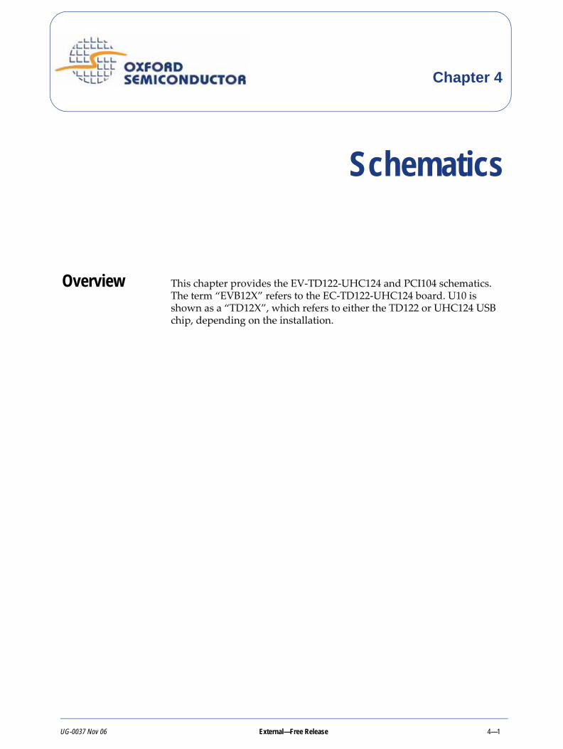
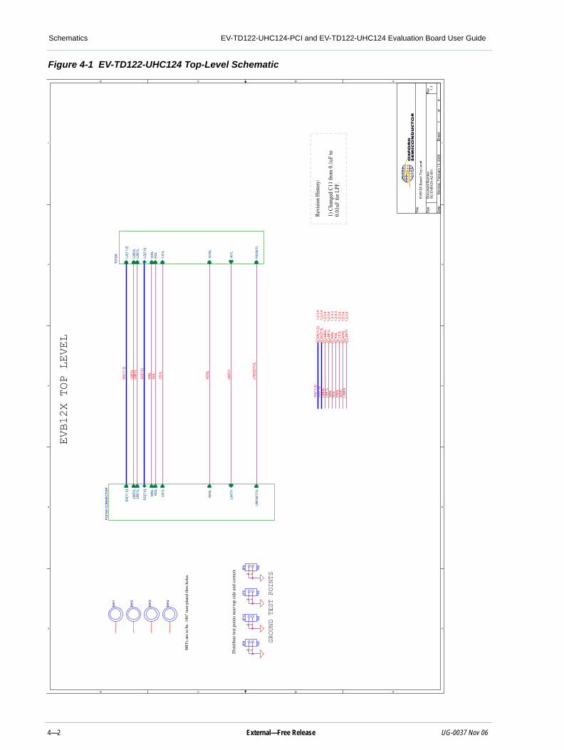
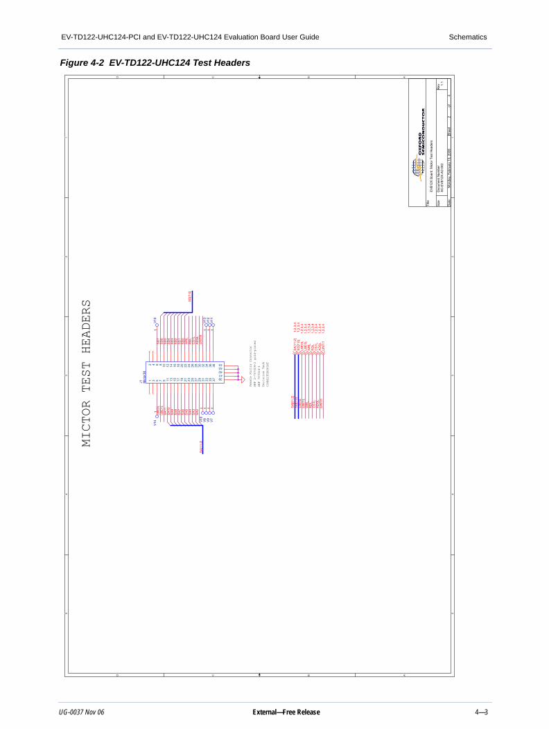
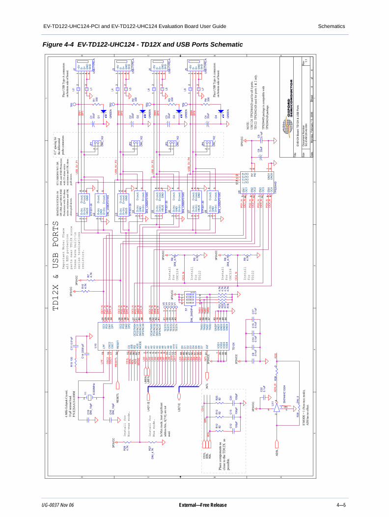
Overview This chapter provides the EV‐TD122‐UHC124 and PCI104 schematics. The term “EVB12X” refers to the EC‐TD122‐UHC124 board. U10 is shown as a “TD12X”, which refers to either the TD122 or UHC124 USB chip, depending on the installation.
UG-0037 Nov 06 External—Free Release 4—1
Schematics EV-TD122-UHC124-PCI and EV-TD122-UHC124 Evaluation Board User Guide
Figure 4-1 EV-TD122-UHC124 Top-Level Schematic
5 5
4 4
3 3
2 2
1 1
DD
CC
BB
AA
EVB12X TOP LEVEL
GROUND TEST POINTS
Dist
ribut
e te
st po
ints
near
top
side
and
corn
ers
MH
's ar
e to
be
.146
" no
n-pl
ated
thru
hol
es.
Revi
sion
Hist
ory:
1) C
hang
ed C
11 fr
om 0
.1uF
to0.
01uF
for L
PF.
SC
-EV
B12
X-A
2-00
11.
1
EV
B12
X B
oard
: Top
Lev
el
14
Mon
day,
Feb
ruar
y 13
, 200
6
Title
Size
Doc
umen
t Num
ber
Rev
Dat
e:S
heet
of
PC
I104
CO
NN
EC
TOR
SA
[11:
2]
SD
[7:0
]
CS
1L
RD
LW
RL
LRE
SE
TOL
LIN
TI1
AD
SL
LBE
0LLB
E1L
TD12
X
WR
LR
DL
RE
SE
TL
CS
1L
LA[1
1:2]
AD
SL
LD[7
:0]
INTL
LBE
0LLB
E1L
CS
1LR
DL
WR
LLB
E1L
LBE
0L
SA
[11:
2]
AD
SL
LIN
TI1
SD
[7:0
]
CS
1L
SD
[7:0
]
LRE
SE
TOL
AD
SL
SA
[11:
2]
LIN
TI1
WR
LR
DL
LBE
0LLB
E1L
LBE
1L1,
2,3,
4
AD
SL
1,2,
3,4
SA
[11:
2]1,
2,3,
4
RD
L1,
2,3,
4C
S1L
1,2,
3,4
LIN
TI1
1,2,
3,4
LBE
0L1,
2,3,
4
WR
L1,
2,3,
4
SD
[7:0
]1,
2,3,
4
MH
1
JP6
1X2
2 1
JP8
1X2
2 1
JP10
1X2
2 1
JP5
1X2
2 1
MH
4
MH
2
MH
3
4—2 External—Free Release UG-0037 Nov 06
EV-TD122-UHC124-PCI and EV-TD122-UHC124 Evaluation Board User Guide Schematics
Figure 4-2 EV-TD122-UHC124 Test Headers5 5
4 4
3 3
2 2
1 1
DD
CC
BB
AA
Female Mictor Connector
AMP 2-767004-2 gold-plated
AMP 767054-1
Emulation Tech
CONMICFEM38SMT
MICTOR TEST HEADERS
SC
-EV
B12
X-A
2-00
21.
1
EV
B12
X B
oard
: Mic
tor T
est H
eade
rs
24
Mon
day,
Feb
ruar
y 13
, 200
6
Title
Size
Doc
umen
t Num
ber
Rev
Dat
e:S
heet
of
CS
1L
LIN
TI1
LBE
0LS
D[7
:0]
RD
L
SA
[11:
2]
WR
L
AD
SL
LBE
1L
SD
4
AD
SL
SD
6
RD
L
SD
0
SD
[7:0
]
LIN
TI1
WR
L
CS
1L
SD
5
SD
1
SD
3
SD
7
SD
2
SA
6
SA
[11:
2]
SA
7
SA
5
SA
10
LBE
1LS
A11
SA
3
SA
8
SA
2
LBE
0L
SA
4
SA
9
LIN
TI1
1,2,
3,4
RD
L1,
2,3,
4C
S1L
1,2,
3,4
SA
[11:
2]1,
2,3,
4
LBE
1L1,
2,3,
4
AD
SL
1,2,
3,4
SD
[7:0
]1,
2,3,
4
WR
L1,
2,3,
4
LBE
0L1,
2,3,
4
J1 Mic
tor3
8
1 3 5 7 9 11 13 15 17 19 21 23 25 27 29 31 33 35 37
2 4 6 8 10 12 14 16 18 20 22 24 26 28 30 32 34 36 38
39
4041
4243
V8
1
V11
1V
71
V13
1V
101
V9
1
V15
1V
141
V12
1
UG-0037 Nov 06 External—Free Release 4—3
Schematics EV-TD122-UHC124-PCI and EV-TD122-UHC124 Evaluation Board User Guide
Figure 4-3 EV-TD122-UHC124 PC104 Connector5 5
4 4
3 3
2 2
1 1
DD
CC
BB
AA
Plac
e byp
ass c
aps n
ear
PC-1
04 co
nnec
tor
Mal
e he
ader
s pla
ced
onth
e bo
ttom
side
of b
oard
.
PCI104 SIGNAL CONNECTOR
Extra Connector, Non-PC104 Standard
Plac
e at P
C104
conn
ecto
r pin
s
Rem
ove
to u
se e
xter
nal 5
Vpo
wer
sup
ply.
Insta
ll re
sisto
r for
3.3
V fro
mPC
I104
Con
necto
r.
5V to 3.3V VoltageConversion
Insta
ll re
sisto
r to
use t
he5V
-to-3
.3V
Regu
lator
.
Power Headers
Power Indicators
Mal
e he
ader
s pla
ced
on th
ebo
ttom
side
of b
oard
.
Non-
mux
Mod
e (M
ode =
1):
Insta
ll R2
3,R2
9,R3
1,R3
3 an
dre
mov
e R2
4,R2
8,R3
2,R3
4.
Mux
Mod
e (M
ode =
0):
Insta
llR2
4,R2
8,R3
2,R3
4 an
dre
mov
e R23
,R29
,R31
,R33
.
SC
-EV
B12
X-A
2-00
31.
1
EV
B12
X B
oard
: PC
I104
Sig
nal C
onne
ctor
34
Mon
day,
Feb
ruar
y 13
, 200
6
Title
Size
Doc
umen
t Num
ber
Rev
Dat
e:S
heet
of
CS
2L
GP
IO2
CS
3LC
S1L
LIN
TI1
LIN
T2
GP
IO_F
SD
CLK
0_R
SD
CK
E0_
R
nPW
E_R
DM
A_E
OT1
GP
IO_P
LD1
GP
IO_P
LD2
GP
IO_A
5P0V
CC
_CO
NN
DM
A_A
CK
0
DM
A_D
RQ
1
SA
2
SD
5
WR
L
SA
6
SD
4
SD
0S
D1
SD
3
LBE
1L
RE
AD
YL
LBE
0L
SD
6
RD
L
SA
8_R
GP
IO1
SA
3S
A4
SA
7
DM
A_A
CK
1
SD
2
DM
A_D
RQ
0
SA
9_R
SD
7LR
ES
ETO
L
SA
10_R
SA
11_R
SA
5
3P3V
_RE
G
SA
6S
A5
SA
7
SA
2
SA
4S
A3
SD
4
SD
2
SD
7
SD
3
SD
5
SD
1S
D0
SD
6
VD
5P0
VD
3P3
DM
A_E
OT0
AD
SL
SD
2S
D1
SD
0
SD
6S
D7
SD
5S
D4
SD
3
LBE
0LLB
E1L
SA
7S
A6
SA
8S
A9
SA
10S
A11
SA
5S
A4
SA
2S
A3
SD
8_R
SD
9_R
SD
10_R
SD
11_R
SD
8_R
SD
9_R
SD
11_R
SD
10_R
SA
8_R
SA
10_R
SA
9_R
SA
11_R
SA
11S
A10
SA
9S
A8
3P3V
CC
_CO
NN
3P3V
CC
_CO
NN
3P3V
CC
3P3V
CC
3P3V
CC
_CO
NN
3P3V
CC
3P3V
CC
3P3V
CC
3P3V
CC
3P3V
CC
3P3V
CC
3P3V
CC
3P3V
CC
3P3V
CC
3P3V
CC
3P3V
CC
5P0V
CC
5P0V
CC
5P0V
CC
_CO
NN
3P3V
CC
5P0V
CC
5P0V
CC
3P3V
CC
3P3V
CC
3P3V
CC
3P3V
CC
3P3V
CC
3P3V
CC
R23
0
R49
0_12
06
V6
1
R11
10K
x 4
1 2 3 45678
R43
DN
I_4.
7K
C21
DN
I_0.
1uF
V23
1
V26
1
R37
DN
I_4.
7K
R34
DN
I_0
C26
0.1u
F+
C25
33uF
V29
1
R16
DN
I_4.
7K
D6
GR
EE
N
R50
10K
x 4
1 2 3 45678
J7
PC
104
32X
2
A1
A2
A3
A4
A5
A6
A7
A8
A9
A10
A11
A12
A13
A14
A15
A16
A17
A18
A19
A20
A21
A22
A23
A24
A25
A26
A27
A28
A29
A30
A31
A32
B1
B2
B3
B4
B5
B6
B7
B8
B9
B10
B11
B12
B13
B14
B15
B16
B17
B18
B19
B20
B21
B22
B23
B24
B25
B26
B27
B28
B29
B30
B31
B32
C7 0.1u
F
R53
150
R31
0
R47
DN
I_0_
1206
J6
PC
104
20X
2
C0
C1
C2
C3
C4
C5
C6
C7
C8
C9
C10
C11
C12
C13
C14
C15
C16
C17
C18
C19
D0
D1
D2
D3
D4
D5
D6
D7
D8
D9
D10
D11
D12
D13
D14
D15
D16
D17
D18
D19
R54
0_12
06R
_120
6
V25
1
C23
0.1u
F
R48
10K
x 4
1 2 3 45678
J8
DN
I_P
C10
4_20
X2
C0
C1
C2
C3
C4
C5
C6
C7
C8
C9
C10
C11
C12
C13
C14
C15
C16
C17
C18
C19
D0
D1
D2
D3
D4
D5
D6
D7
D8
D9
D10
D11
D12
D13
D14
D15
D16
D17
D18
D19
R44
DN
I_4.
7K
R32
DN
I_0
C27 0.1u
F
V30
1
V21
1
V33
1
TP5
R30
10K
x 4
1 2 3 45678
V32
1
V16
1
D5
GR
EE
N
R56
330
R33
0V
311
V24
1
R41
4.7K
U12
LMS
1587
IS-3
.3
3
1
2 4V
IN
GND
VO
UT
TAB
V20
1
R39
DN
I_4.
7K
C6 0.1u
F
R28
DN
I_0
V19
1
V22
1R52
4.7K
V28
1
+C
244.
7uF
+C
284.
7uF
R42
DN
I_4.
7K
R45
DN
I_4.
7K
R19
DN
I_4.
7K
JP7
1X3
3 2 1
R29
0
R22
10K
x 4
1 2 3 45678
V18
1
R46
DN
I_4.
7K
V17
1
R24
DN
I_0
R55
0_12
06R
_120
6
+C
18D
NI_
4.7u
F
R40
DN
I_4.
7K
R35
4.7K
JP9
1X3
3 2 1
V27
1
R14
4.7K
R51
DN
I_4.
7K
RD
LW
RL
CS
1L
LRE
SE
TOL
LIN
TI1
AD
SL
LBE
1LLB
E0L
SD
[7:0
]
SA
[11:
2]
4—4 External—Free Release UG-0037 Nov 06
EV-TD122-UHC124-PCI and EV-TD122-UHC124 Evaluation Board User Guide Schematics
Figure 4-4 EV-TD122-UHC124 - TD12X and USB Ports Schematic5 5
4 4
3 3
2 2
1 1
DD
CC
BB
AA
TD12X & USB PORTS
6 M
Hz E
clipt
ek C
rysta
l,18
pF
inter
nal l
oad.
P/
N:E2
SAA1
8-6.
000M
Install
for
TD122
Install
for
UHC124
Install
for
TD122
NOTE
:U
HC1
24: T
PS20
44A
D us
ed fo
r all
4 po
rts.
TD12
2: T
PS20
42A
D u
sed
for p
orts
1 &
2 o
nly.
TPS2
044D
pac
kage
is co
mpa
tible
with
TPS2
042A
D pa
ckag
e.
Install
for
UHC124
0.1"
spac
ing
for
the d
iffer
entia
lpr
obe c
onne
ctors
If M
ODE
= 1
(Non
-mux
mod
e),
ADS
has n
o ef
fect.
Install for
Non-mux mode.
Install for
Mux mode.
Plac
e co
mpo
nent
s as
clos
e to
the
TD12
X a
spo
ssib
le.
SEM
TEC
H S
TF20
1-30
:D
P, D
M, a
nd V
BU
S ES
DPr
otec
tion
with
30
ohm
sse
ries
resi
stan
ce a
nd 1
5Koh
ms
pull-
dow
n.
Plac
e USB
Typ
e-A
conn
ecto
rson
bot
tom
side
of b
oard
.
Plac
e USB
Typ
e-A
conn
ecto
rson
bot
tom
side
of b
oard
.Important Note: Place
all ESD protection
parts near TD12X since
these have built-in
series terminations
resistors.
In M
ux m
ode,
least
signi
fican
tad
dres
s bits
, A[7
:0],
are n
otus
ed.
ST U
SBD
F01W
5: D
P,D
M, a
nd E
SD P
rote
ctio
nw
ith 3
3 oh
ms s
erie
sre
sist
ance
and
15K
ohm
spu
ll-do
wn.
SC
-EV
B12
X-A2
-004
1.1
EV
B12
X B
oard
: TD
12X
& U
SB
Por
ts
44
Mon
day,
Feb
ruar
y 13
, 200
6
Title
Size
Doc
umen
t Num
ber
Rev
Dat
e:S
heet
of
US
B_5
V_P
2
US
B_5
V_P
3
WR
L LA1
DP
4_R
LD4
PO
3_N
OC
2_N
LPF LA
6
OC
2_N
DM
4_R
LD5
OC
1_N
PO
2_N
DM
2_R
LD1
LA7
LD3
LD0
RD
L LA5
PO
4_N
LA3
PO
2_N
LA10
CS
1L INTL
PO
4_N
OC
3_N
LD7
LD2
PO
1_N
PO
3_N
DP
2_R
LA11
DM
1_R
LA8
LA2
LA4
LA0
DP
3_R
OS
C2
LD6
DP
1_R
RE
SE
TL
DM
3_R
PO
1_N
LA9
AD
S
OC
4_N
OC
4_N
OC
4_N
OC
3_N
DM
1D
P1
DM
2
DM
3D
P3
MO
DE
CS
1LW
RL
RD
L
OC
3_N
US
B_5
V_P
4D
M4
DP
4
TMS0
DP
2
TMS3
TMS1
TMS2
AD
S_R
AD
S
OS
C1
US
B_5
V_P
1
OC
1_N
3P3V
CC
3P3V
CC
3P3V
CC
5P0V
CC
3P3V
CC
3P3V
CC
3P3V
CC
3P3V
CC
3P3V
CC
3P3V
CC
B L7
12
2200
pF
C14
R36
DN
I_0
U7
STF
201-
30
1654
23
VB
US
GN
DD
+(ou
t)D
-(ou
t)D
+(In
)D
-(In
)
R3
330
TP3
R12
82
D1
GR
EE
N
B L1
12
C11
0.01
uF
V5
1
R6
DN
I_4.
7K
C15
0.1u
F
BL6
12
B L3
12
C13
100p
F
Y1
6.00
0MH
z
12
US
B-T
YP
E-A
J2
321 4 5
D+
D-
+5V
GN
DS
HD
TP4
S1
DN
I_S
WD
IP-4
1234
8765
D2
GR
EE
N
C9
0.1u
F
US
B-T
YP
E-A
J5
321 4 5
D+
D-
+5V
GN
DS
HD
U9
TPS
2044
D
3 4 7 816 13 12 9
10111415
2 6 51
EN
1
EN
2
EN
3
EN
4
OC
1
OC
2
OC
3
OC
4
OUT4OUT3OUT2OUT1
IN1
IN2
GN
D5
GN
D1
C5
0.1u
F
R20
4.7K
R1
330
JP2
DN
I_1X
2
2 1
V4
1
+C
433
uF
U6
DN
I_U
SB
DF0
1W5
254
13G
ND
D+(
out)
D-(
out)
D+(
In)
D-(
In)
R5
4.7K
C12
100p
F
C17
0.1u
F
TP2
U11 S
N74
AH
C1G
04
42
5 3NC_1
JP1
DN
I_1X
2
2 1
TP1
D3
GR
EE
N
C22
0.1u
F
R9
4.7K
C19
DN
I_10
pF
+C
333
uFV
31
U5
STF
201-
30
1654
23
VB
US
GN
DD
+(ou
t)D
-(ou
t)D
+(In
)D
-(In
)
+C
133
uF
R4
330
BL2
12
JP3
DN
I_1X
2
2 1
C20
100p
F
+C
233
uF
BL8
12
R38
0
BL4
12
U1
STF
201-
30
1654
23
VB
US
GN
DD
+(ou
t)D
-(ou
t)D
+(In
)D
-(In
)
R18
4.7K
R17
4.7K
R7
4.7K
V2
1
R15
100
B L5
12
C16
DN
I_10
pF
R8
DN
I_4.
7K
U2
DN
I_U
SB
DF0
1W5
254
13G
ND
D+(
out)
D-(
out)
D+(
In)
D-(
In)
R25
82
JP4
DN
I_1X
2
2 1
U4
DN
I_U
SB
DF0
1W5
254
13G
ND
D+(
out)
D-(
out)
D+(
In)
D-(
In)
US
B-T
YP
E-A
J4
321 4 5
D+
D-
+5V
GN
DS
HD
D4
GR
EE
N
V1
1
R10
4.7K
R2
330
R26
4.7K
+C
833
uF
C10
0.1u
F
R27
DN
I_4.
7K
R13
82
U8
DN
I_U
SB
DF0
1W5
254
13G
ND
D+(
out)
D-(
out)
D+(
In)
D-(
In)
U10
TD12
X
171819 54 15 55 56 62 14 1312111098765432 5352515047464544
644916 36201 33 48
4324232221 60 59 58 5734 3735 38
61
302925 26 6327 2831 323940 4142
OS
C1
OS
C2
LPF
RE
SE
T
CS
WR
RD
AD
SM
OD
E
A11
A10
A9
A8
A7
A6
A5
A4
A3
A2
A1
A0
D7
D6
D5
D4
D3
D2
D1
D0
GN
D4
GN
D3
GN
D1
GN
D2
VD
D2
VD
D1
VD
D3
VD
D4
TES
T4TE
ST3
TES
T2TE
ST1
TES
T0
TMS
3TM
S2
TMS
1TM
S0
DP
1
DP
2
DM
1
DM
2
INT
PO
2
PO
1O
C1
OC
2
GN
DP
OC
3/TM
S4
OC
4/TM
S5
PO
3/N
C31
PO
4/N
C32
DP
3/N
C39
DM
3/N
C40
DP
4/N
C41
DM
4/N
C42
US
B-T
YP
E-A
J3
321 4 5
D+
D-
+5V
GN
DS
HD
R21
4.7K
U3
STF
201-
30
1654
23
VB
US
GN
DD
+(ou
t)D
-(ou
t)D
+(In
)D
-(In
)
AD
SL
LBE
0L
LD[7
:0]
INTL
LBE
1LLA
[11:
2]RE
SE
TL
RD
L
CS
1LW
RL
UG-0037 Nov 06 External—Free Release 4—5
Schematics EV-TD122-UHC124-PCI and EV-TD122-UHC124 Evaluation Board User Guide
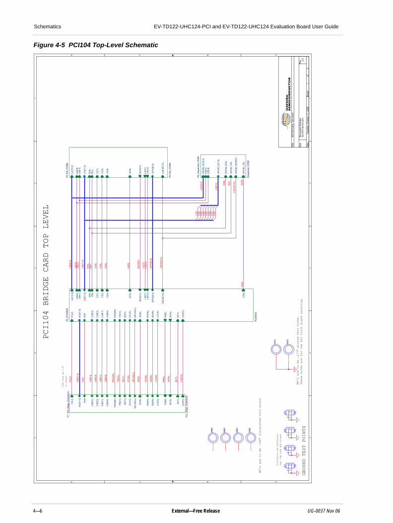
Figure 4-5 PCI104 Top-Level Schematic
5 5
4 4
3 3
2 2
1 1
DD
CC
BB
AA
PCI104 BRIDGE CARD TOP LEVEL
PCLK must be 2.5"
in length
GROUND TEST POINTS
Distribute the TestPoints
near top side and corners
MH's are to be .146" non-plated thru holes.
MH's are to be .177" plated thru holes.
These holes are for the PCI front plate mounting.
SC
-PC
I104
-A1-
001
2.0
PC
I104
Car
d: T
op L
evel
15
Tues
day,
Oct
ober
17,
200
6
Title
Size
Doc
umen
t Num
ber
Rev
Dat
e:S
heet
of
PC
104_
CO
NN
PC
104_
CO
NN
WR
LR
DL
LIN
TI2
LRE
SE
TOL
CS
2L
CS
1L
LA[1
9:2]
RE
AD
YL
AD
SL
LD[3
1:0]
GP
IO[8
:4]
CS
3L
LIN
TI1
LBE
0LLB
E1L
P1_
PC
I_E
dge_
Con
nect
or
PC
I_E
dge_
Con
nect
or
PC
LK
AD
[31:
0]
C/B
E3L
C/B
E2L
IRD
YL
DE
VS
ELL
LOC
KL
PE
RR
L
SE
RR
L
C/B
E1L
VIO
PC
I
C/B
E0L
PA
R
STO
PL
FRA
ME
L
TRD
YL
IDS
EL
RS
TL
INTA
L
PM
EL
P2_
PLX9
030
PLX9
030
LD[3
1:0]
VIO
PC
I
PC
LK
RS
TL
IDS
EL
C/B
E0L
AD
[31:
0]
C/B
E1L
C/B
E2L
C/B
E3L
FRA
ME
L
IRD
YL
TRD
YL
STO
PL
DE
VS
ELL
PE
RR
L
SE
RR
L
LOC
KL
PA
R
INTA
L
PM
EL
AD
SL
RD
LW
RL
RE
AD
YL
LRE
SE
TOL
CS
0L
CS
1L
CS
2L
LIN
TI1
LA[1
9:2]
CS
3L
GP
IO[8
:4]
LBE
0LLB
E1L
LIN
TI2
P6_
Exp
ansi
on_R
OM
Exp
ansi
on_R
OM
XR
OM
_A[1
9:2]
XR
OM
_D[7
:0]
XR
OM
_CEL
XRO
M_O
EL
XR
OM
_WEL
XR
OM
_RES
ETL
LBE
1LLB
E0L
C/B
E2L
VIO
PC
I
AD
[31:
0]
IRD
YL
LOC
KL
PM
EL
C/B
E0L
C/B
E3L
INTA
L
RE
AD
YL
RS
TL
DE
VS
ELL
LRE
SE
TOL
CS
1L
IDS
EL
PA
R
PC
LK
TRD
YL
PE
RR
L
SE
RR
L
AD
SL
CS
2LC
/BE
1L
FRA
ME
L
STO
PL
LIN
TI1
CS
3L
GP
OI[8
:4]
LBE
0L
LA[1
9:2]
LIN
TI2
WR
L
LD4
RD
L
LD3
LD6
LA[1
9:2]
RD
L
LD[7
:0]
LD1
LD5
LD0
WR
L
LD2
LBE
1L
LD7
LD[3
1:0]
CS
0LC
S0L
LRE
SE
TOL
MH
6
MH
4
JP3
1X2
2 1M
H2
MH
1
JP1
1X2
2 1
JP5
1X2
2 1
JP6
1X2
2 1
MH
3
MH
5
4—6 External—Free Release UG-0037 Nov 06
EV-TD122-UHC124-PCI and EV-TD122-UHC124 Evaluation Board User Guide Schematics
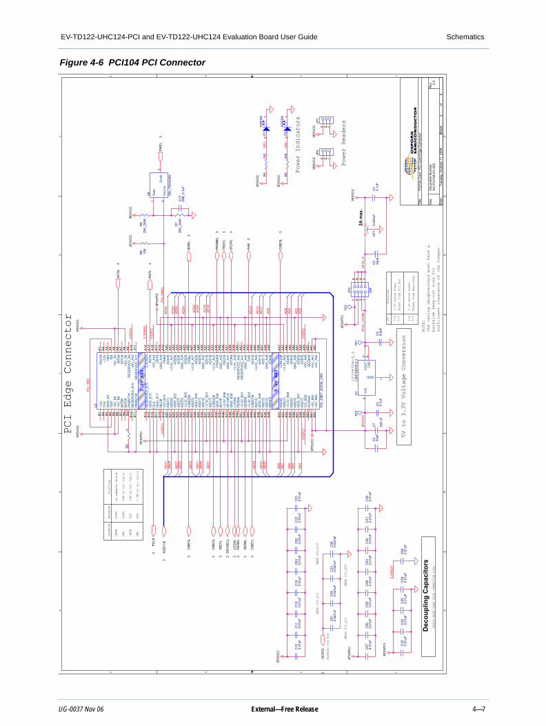
Figure 4-6 PCI104 PCI ConnectorA A
B B
C C
D D
E E
44
33
22
11
5V to 3.3V VoltageConversion
Deco
up
lin
g C
ap
acit
ors
PRSNT1#
PRSNT2#
Function
GND
OPEN
OPEN
GND
GND
OPEN
OPEN
GND
no adapter board
15W on all rails
25W on all rails
7.5W on all rails
Power Indicators
NEAR VIO_A10
NEAR VIO_A16
NEAR VIO_A59
NEAR VIO_B19
PLACE NEAR CARD EDGE CONNECTOR PINS
PLX9030 VIO PIN
Power Headers
7-8
5-6
3-4
1-2
3.3V Board Power
Taken from PCI Bus
3.3V Board Power
Taken from Regulator
JP
Function
NOTE:
The mating daughtercard must have a
backside keep-out area for
sufficient clearance of the Jumper.
LT1587CM-3.3
2A
max.
PCI Edge Connector
SC
-PC
I104
-A1-
002
2.0
PC
I104
Car
d : P
CI C
ard
Edg
e C
onne
ctor
25
Tues
day,
Oct
ober
17,
200
6
Title
Size
Doc
umen
t Num
ber
Rev
Dat
e:S
heet
of
VIO
PC
I
3.3V
AU
X
VIO
PC
I
VIO
PC
I
PC
I_P
ME
L
VIO
PC
I
VIO
PC
I
3.3V
AU
X
VD
5
VD
3
PC
I_TD
D
5P0V
CC
AD
25
AD
16
AD
8
AD
12A
D13
AD
30A
D29
AD
6
AD
18
AD
23
AD
1
AD
22
AD
31
AD
26
AD
14
AD
10
AD
0
AD
19A
D21
AD
17
AD
4
AD
7
AD
9
AD
28
AD
24
AD
2
AD
15
AD
11
AD
27
AD
3A
D5
AD
20
3P3V
_CO
NN
3P3V
_S
5P0V
CC
5P0V
CC
3P3V
CC
5P0V
CC
3P3V
PC
I
3P3V
PC
I
3P3V
PC
I
3P3V
PC
I
3P3V
PC
I
5P0V
CC
5P0V
CC
3P3V
CC
5P0V
CC
3P3V
CC
3P3V
CC
3P3V
CC
C56
0.01
uF
TP2
C24
0.01
uF
C19
0.01
uF
C57
0.01
uF
C59
0.04
7uF
C3
0.1u
F
+C
433
uF
C25
0.01
uF
R7
DN
I_24
0K
C22
0.01
uF
C58
0.04
7uF
+C
233
uFC
10.
1uF
3.3V KEY
5.0V KEY
U2
PC
I_32
BIT
_ED
GE
_UN
V
A1
B1
A2
B2
A3
B3
A4
B4
A5
B5
A6
B6
A7
B7
A8
B8
A9
B9
A10
B10
A11
B11
A14
B14
A15
B15
A16
B16
A17
B17
A18
B18
A19
B19
A20
B20
A21
B21
A22
B22
A23
B23
A24
B24
A25
B25
A26
B26
A27
B27
A28
B28
A29
B29
A30
B30
A31
B31
A32
B32
A33
B33
A34
B34
A35
B35
A36
B36
A37
B37
A38
B38
A39
B39
A40
B40
A41
B41
A42
B42
A43
B43
A44
B44
A45
B45
A46
B46
A47
B47
A48
B48
A49
B49
A52
B52
A53
B53
A54
B54
A55
B55
A56
B56
A57
B57
A58
B58
A59
B59
A60
B60
A61
B61
A62
B62
TRS
T#-1
2V+1
2VTC
KTM
SG
ND
_B3
TDI
TDO
+5V
_A5
+5V
_B5
INTA
#+5
V_B
6IN
TC#
INTB
#+5
V_A
8IN
TD#
RE
SE
RV
ED
_A9
PR
SN
T1#
VIO
_A10
RE
SE
RV
ED
_B10
RE
SE
RV
ED
_A11
PR
SN
T2#
3.3V
AU
XR
ES
ER
VE
D_B
14R
ST#
GN
D_B
15V
IO_A
16C
LKG
NT#
GN
D_B
17G
ND
_A18
RE
Q#
PM
E#
VIO
_B19
AD
[30]
AD
[31]
+3.3
V_A
21A
D[2
9]A
D[2
8]G
ND
_B22
AD
[26]
AD
[27]
GN
D_A
24A
D[2
5]A
D[2
4]+3
.3V
_B25
IDS
EL
C/B
E[3
]#+3
.3V
_A27
AD
[23]
AD
[22]
GN
D_B
28A
D[2
0]A
D[2
1]G
ND
_A30
AD
[19]
AD
[18]
+3.3
V_B
31A
D[1
6]A
D[1
7]+3
.3V
_A33
C/B
E[2
]#FR
AM
E#
GN
D_B
34G
ND
_A35
IRD
Y#
TRD
Y#
+3.3
V_B
36G
ND
_A37
DE
VS
EL#
STO
P#
GN
D_B
38+3
.3V
_A39
LOC
K#
RE
SE
RV
ED
_A40
PE
RR
#R
ES
ER
VE
D_A
41+3
.3V
_B41
GN
D_A
42S
ER
R#
PA
R+3
.3V
_B43
AD
[15]
C/B
E[1
]#+3
.3V
_A45
AD
[14]
AD
[13]
GN
D_B
46A
D[1
1]A
D[1
2]G
ND
_A48
AD
[10]
AD
[09]
M66
EN
C/B
E[0
]#A
D[0
8]+3
.3V
_A53
AD
[07]
AD
[06]
+3.3
V_B
54A
D[0
4]A
D[0
5]G
ND
_A56
AD
[03]
AD
[02]
GN
D_B
57A
D[0
0]A
D[0
1]V
IO_A
59V
IO_B
59R
EQ
64#
AC
K64
#+5
V_A
61+5
V_B
61+5
V_A
62+5
V_B
62JP
73 2 1
U1
LMS
1587
IS-3
.3
3
1
2 4V
IN
GND
VO
UT
TAB
R9
DN
I_24
0K
JP4
3 2 1
TP3
R5
300
C32
0.01
uF
C36
0.01
uF
C11
0.01
uF
+C
56.
8uF
C41
0.01
uF
C23
0.04
7uF
C7
220
uF
R4
150
C42
0.01
uF
R8 10K
C13
DN
I_0.
1uF
C35
0.01
uF
D1
GR
EE
N2
1
U6
DN
I_FD
N33
5N
3
1 2D
rain
Gat
e
Sou
rce
C10
0.01
uF
TP1
D2
GR
EE
N2
1
C43
0.01
uF
C62
0.01
uF
CF1
0.02
2uF
C61
0.04
7uF
C63
0.01
uF
C48
0.01
uF
C18
0.01
uF
R6
0
C50
0.01
uF
C21
0.01
uF
C60
0.01
uF
JP2
2X4
21
4357
8 6
PC
LK3 A
D[3
1:0]
3
C/B
E3L
3
C/B
E2L
3
IRD
YL
3
DE
VS
ELL
3
LOC
KL
3P
ER
RL
3
SE
RR
L3
C/B
E1L
3
C/B
E0L
3
PA
R3
STO
PL3
FRA
ME
L3
TRD
YL
3
IDS
EL
3
RS
TL3
INTA
L3
PM
EL3
VIO
PC
I3
UG-0037 Nov 06 External—Free Release 4—7
Schematics EV-TD122-UHC124-PCI and EV-TD122-UHC124 Evaluation Board User Guide
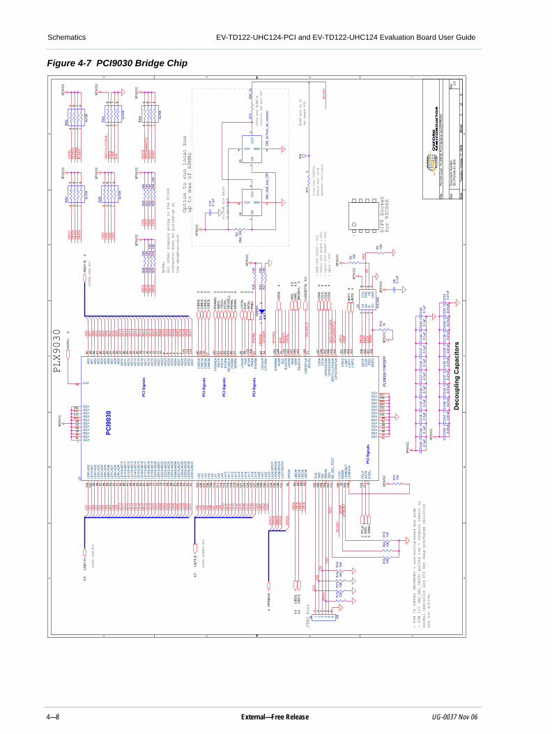
Figure 4-7 PCI9030 Bridge Chip
A A
B B
C C
D D
E E
44
33
22
11
JTAG Port
- PIN 76 (MODE) GROUNDED = non-multiplexed bus mode
- PIN 112 (BD_SEL_TEST) pulled low = outputs remain in
normal operation and PCI Hot Swap precharge resistors
are not active.
De
co
up
lin
g C
ap
ac
ito
rs
+ XROM CHIP SELECT = CS0L
+ OTG243 CHIP SELECT = CS1L
+ ispLSI CHIP SELECT = CS2L
+ spare = CS3L
LOCAL DATA BUS
LOCAL ADDRESS BUS
SYSTEM DATA BUS
BCLK0 must be 2X
the length CS1L
NOTE:
All other signals going to the PC104
connector must be pulled-up on
the daughtercard.
ECLIPTEK EC28 SERIES
OR EQUIVALENT
Place near PLX9030.
Remove when using
external oscillator.
Place near BCLKO_R
resistor and near OSC
Option to run local bus
up to max of 60MHz
DIP8 Socket
for 93CS66
1
PLX9030
SC
-PC
I104
-A1-
003
2.0
PC
I104
Car
d : P
LX90
30 P
CI I
nter
face
and
EE
PR
OM 3
5Tu
esda
y, O
ctob
er 1
7, 2
006
Title
Size
Doc
umen
t Num
ber
Rev
Dat
e:S
heet
of
PR
E
BTE
RM
LR
EA
DY
LLW
/RL
PE
TMS
LA21
GP
IO6
AD
11
LRE
QAD
0
AD
14
AD
18
LBE
0L
MO
DE
GP
IO0/
WA
ITO
L
TDI
LA22
AD
8
AD
16
AD
28
AD
31
LA23
AD
13
AD
22
EN
UM
L
BC
LKO
EE
SKA
D29
LPM
ESET
AD
9
AD
26
AD
30
LBE
3L
EE
CSA
D24
EE
DOA
D1
ALE
GP
IO7
AD
23
AD
4
AD
17
LBE
2L
TEST
TRS T
L
AD
10
AD
12
TDO
AD
3
GP
IO1/
LLO
CK
OL
GP
IO4
AD
25
AD
27
BLA
STL
AD
19A
D20
GP
IO5
AD
7
AD
21
AD
6
LA20
AD
2
AD
5
AD
15
TCK
LW/R
L
BTE
RM
L
EE
DI
LED
ON
L
LD1
LD27
LA9
LD12
LD16
LD14
LD15
LA5
LA8
LD19
LD23
LD4
LD28
LA6
LA18
LD25
LD6
LD0
LD24
LA16
LD2
LD9
LD13
LD29
LA4
LD8
LA12
LD7
LA10
LA14
LD10
LA3
LD20
LD17
LD22
LD21
LA17
LD3
LA7
LA15
LD26
LD30
LA19
LD18
LA13
LD31
LA11
LD11
LA2
LD5
CP
CIS
W
LGN
T
GP
IO8
BC
LKO
_R
BLA
STL
GP
IO0/
WA
ITO
L
ALE
GP
IO1/
LLO
CK
OL
LGN
TLR
EQ
GP
IO5
GP
IO4
GP
IO6
GP
IO7
LA21
LA23
LA22
LA20
GP
IO8
LBE
1L
LIN
TI2
LIN
TI1
CS
0LC
S1L
CS
2LC
S3L
BC
LKO
LBE
2LLB
E1L
LBE
0L
LBE
3L
3P3V
CC
3P3V
CC
3P3V
CC
3P3V
CC
3P3V
CC
3P3V
CC
3P3V
CC
3P3V
CC
3P3V
CC
3P3V
CC
3P3V
CC
3P3V
CC
3P3V
CC
3P3V
CC
3P3V
CC
3P3V
CC
3P3V
CC
C28
0.1u
F
R31
150
R17
10K
R1
10K
C34
0.01
uF
R18
10K
C31
0.01
uF
PC
I S
ign
als
PC
I S
ign
als
PC
I S
ign
als
PC
I S
ign
als
PC
I S
ign
als
PC
I90
30
U7
PLX9
030-
176P
QFP
152
144
143
151
139
154
150
153
138
142
158
172
140
160
161
171 8
112
145 76
149
60 59 58 55
51169
10 155
56
52173
174
175
23416171830333435363738394142434647484950 5
4532
85
101100
70
13
117133
31
162
170
57
111215 9 28
66
44
6
78
257
88
2019
113
22
122
21
132
29
146
2440 23
128
26 27
137
136
135
13484 131
130
12995 127
125
124
12393 12192 120
119
118
11691 115
114
11190 110
109
108
10789 106
10587 86 83 81104 80102 7999 98 7797 96 74 73 72 69 68 6782 65 64 63 62 61
114
163176
159
165
166
168
164
167
53
75 141
94
147
148
157
156
54 71
103
126
LIN
Ti1
BTE
RM
#
RE
AD
Y#
LRE
Q
BLA
ST#
GP
IO0/
WA
ITo#
LGN
T
LIN
Ti2
AD
S#
LW/R
#
EE
CS
PC
LK
WR
#
EE
SK
EE
DI
RS
T#ID
SE
L
BD
_SE
L_TE
ST
LCLK
MO
DE
LRE
SE
To#
LBE
0#LB
E1#
LBE
2#LB
E3#
EN
UM
#P
ME
#
AD
22
GP
IO1/
LLO
CK
o#
VDD
LED
on#
AD
31A
D30
AD
29A
D28
AD
27A
D26
AD
18A
D17
AD
16A
D15
AD
14A
D13
AD
12A
D11
AD
10A
D9
AD
8A
D7
AD
6A
D5
AD
4A
D3
AD
2A
D1
AD
0
AD
25
VDDVDD
VDD
VSSVDD
VDD
VSS
VDDVDD
VSS
VDD
INTA
#
VSS
AD
21A
D20
AD
19
AD
23
PA
R
VSS
VSS
AD
24
VSS
LOC
K#
C/B
E3#
VSS
FRA
ME
#
C/B
E2#
VSS
TRD
Y#
VSS
IRD
Y#
VSS
C/B
E1#
VSS
STO
P#
C/B
E0#
DE
VS
EL#
LA20
PE
RR
#S
ER
R#
LA27
/GP
IO4
LA26
/GP
IO5
LA25
/GP
IO6
LA24
/GP
IO7
LD14
/LA
D14
LA23
LA22
LA21
LD6/
LAD
6
LA19
LA18
LA17
LA16
LD7/
LAD
7
LA15
LD8/
LAD
8
LA14
LA13
LA12
LA11
LD9/
LAD
9
LA10
LA9
LA8
LD10
/LA
D10
LA7
LA6
LA5
LA4
LD11
/LA
D11
LA3
LA2
LD12
/LA
D12
LD13
/LA
D13
LD15
/LA
D15
LD17
/LA
D17
LD0/
LAD
0
LD18
/LA
D18
LD1/
LAD
1
LD19
/LA
D19
LD2/
LAD
2LD
3/LA
D3
LD20
/LA
D20
LD4/
LAD
4LD
5/LA
D5
LD21
/LA
D21
LD22
/LA
D22
LD23
/LA
D23
LD24
/LA
D24
LD25
/LA
D25
LD26
/LA
D26
LD16
/LA
D16
LD27
/LA
D27
LD28
/LA
D28
LD29
/LA
D29
LD30
/LA
D30
LD31
/LA
D31
VDDVDD
VSSVSS
EE
DO
TCK
TMS
TDI
TRS
T#TD
O
VI/O
ALE
RD
#G
PIO
8
CS
0#C
S1#
GP
IO3/
CS
3#G
PIO
2/C
S2#
CP
CIS
W
BC
LKo
LPM
ES
ET
LPM
INT#
C33
0.1u
F
J4 1X6
1 2 3 4 5 6
1 2 3 4 5 6
R28
10K
R11
0
C40
0.01
uF
C54
0.1u
F
C53
0.01
uF
R23
10K
R12
1K
C15
0.1u
F
D3G
RE
EN
21
R29
DN
I_10
K
R14
10K
C39
0.1u
F
C47
0.01
uF
C9
0.1u
F
C44
0.1u
F
RN
4 4x10
K
12345 6 7 8
R19
10K
U5
DN
I_5x
7mm
_sm
_cer
amic
1
2
3
4
EN
GND
OU
T
VCC
R13
10K
U3
93C
S66
1 2 3 4
8 7 6 5
CS
SK
DI
DO
VC
CP
RE
PE
GN
D
R26
10K
RN
2 4x10
K
12345 6 7 8
TP4
R22
10K
C37
0.1u
FC
270.
1uF
RN
3 4x10
K
12345 6 7 8
RN
1 4x10
K
12345 6 7 8
C29
0.01
uF
C26
0.1u
F
R3
10K
R21
10K
R15
10K
R27
10K
C52
0.1u
F
R2
DN
I_10
K
R10
DN
I_33
C30
0.01
uF
R24
10K
RN
5 4x10
K
12345 6 7 8
C49
0.1u
FC
460.
1uF
R20
DN
I_10
K
C45
0.01
uF
U4
DN
I_H
alf_
size
_DIP
1
4
5
8
EN
GND
OU
T
VCC
R25
DN
I_10
K
C55
0.01
uFC
510.
01uF
R16
10K
R30
10K
C38
0.01
uF
LD[3
1:0]
4,5
PC
LK2
RS
TL2
IDS
EL
2
C/B
E0L
2
AD
[31:
0]2
C/B
E1L
2C
/BE
2L2
C/B
E3L
2
FRA
ME
L2
IRD
YL
2TR
DY
L2
STO
PL2
DE
VS
ELL
2
LOC
KL
2P
AR
2IN
TAL
2PM
EL2
AD
SL
4
RD
L4,
5W
RL
4,5
RE
AD
YL
4
LRE
SE
TOL
4,5
CS
0L5
CS
1L4
CS
2L4
LIN
TI1
4
LA[1
9:2]
4,5
SE
RR
L2
PE
RR
L2
VIO
PC
I2
CS
3L4
GP
IO[8
:4]
4
LBE
0L4,
5LB
E1L
4,5
LIN
TI2
4
4—8 External—Free Release UG-0037 Nov 06
EV-TD122-UHC124-PCI and EV-TD122-UHC124 Evaluation Board User Guide Schematics
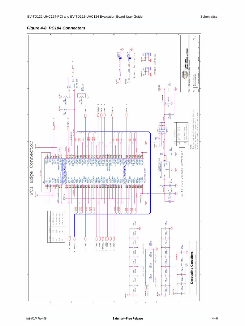
Figure 4-8 PC104 ConnectorsA A
B B
C C
D D
E E
44
33
22
11
5V to 3.3V VoltageConversion
Deco
up
lin
g C
ap
acit
ors
PRSNT1#
PRSNT2#
Function
GND
OPEN
OPEN
GND
GND
OPEN
OPEN
GND
no adapter board
15W on all rails
25W on all rails
7.5W on all rails
Power Indicators
NEAR VIO_A10
NEAR VIO_A16
NEAR VIO_A59
NEAR VIO_B19
PLACE NEAR CARD EDGE CONNECTOR PINS
PLX9030 VIO PIN
Power Headers
7-8
5-6
3-4
1-2
3.3V Board Power
Taken from PCI Bus
3.3V Board Power
Taken from Regulator
JP
Function
NOTE:
The mating daughtercard must have a
backside keep-out area for
sufficient clearance of the Jumper.
LT1587CM-3.3
2A
max.
PCI Edge Connector
SC
-PC
I104
-A1-
002
2.0
PC
I104
Car
d : P
CI C
ard
Edg
e C
onne
ctor
25
Tues
day,
Oct
ober
17,
200
6
Title
Size
Doc
umen
t Num
ber
Rev
Dat
e:S
heet
of
VIO
PC
I
3.3V
AU
X
VIO
PC
I
VIO
PC
I
PC
I_P
ME
L
VIO
PC
I
VIO
PC
I
3.3V
AU
X
VD
5
VD
3
PC
I_TD
D
5P0V
CC
AD
25
AD
16
AD
8
AD
12A
D13
AD
30A
D29
AD
6
AD
18
AD
23
AD
1
AD
22
AD
31
AD
26
AD
14
AD
10
AD
0
AD
19A
D21
AD
17
AD
4
AD
7
AD
9
AD
28
AD
24
AD
2
AD
15
AD
11
AD
27
AD
3A
D5
AD
20
3P3V
_CO
NN
3P3V
_S
5P0V
CC
5P0V
CC
3P3V
CC
5P0V
CC
3P3V
PC
I
3P3V
PC
I
3P3V
PC
I
3P3V
PC
I
3P3V
PC
I
5P0V
CC
5P0V
CC
3P3V
CC
5P0V
CC
3P3V
CC
3P3V
CC
3P3V
CC
C56
0.01
uF
TP2
C24
0.01
uF
C19
0.01
uF
C57
0.01
uF
C59
0.04
7uF
C3
0.1u
F
+C
433
uF
C25
0.01
uF
R7
DN
I_24
0K
C22
0.01
uF
C58
0.04
7uF
+C
233
uFC
10.
1uF
3.3V KEY
5.0V KEY
U2
PC
I_32
BIT
_ED
GE
_UN
V
A1
B1
A2
B2
A3
B3
A4
B4
A5
B5
A6
B6
A7
B7
A8
B8
A9
B9
A10
B10
A11
B11
A14
B14
A15
B15
A16
B16
A17
B17
A18
B18
A19
B19
A20
B20
A21
B21
A22
B22
A23
B23
A24
B24
A25
B25
A26
B26
A27
B27
A28
B28
A29
B29
A30
B30
A31
B31
A32
B32
A33
B33
A34
B34
A35
B35
A36
B36
A37
B37
A38
B38
A39
B39
A40
B40
A41
B41
A42
B42
A43
B43
A44
B44
A45
B45
A46
B46
A47
B47
A48
B48
A49
B49
A52
B52
A53
B53
A54
B54
A55
B55
A56
B56
A57
B57
A58
B58
A59
B59
A60
B60
A61
B61
A62
B62
TRS
T#-1
2V+1
2VTC
KTM
SG
ND
_B3
TDI
TDO
+5V
_A5
+5V
_B5
INTA
#+5
V_B
6IN
TC#
INTB
#+5
V_A
8IN
TD#
RE
SE
RV
ED
_A9
PR
SN
T1#
VIO
_A10
RE
SE
RV
ED
_B10
RE
SE
RV
ED
_A11
PR
SN
T2#
3.3V
AU
XR
ES
ER
VE
D_B
14R
ST#
GN
D_B
15V
IO_A
16C
LKG
NT#
GN
D_B
17G
ND
_A18
RE
Q#
PM
E#
VIO
_B19
AD
[30]
AD
[31]
+3.3
V_A
21A
D[2
9]A
D[2
8]G
ND
_B22
AD
[26]
AD
[27]
GN
D_A
24A
D[2
5]A
D[2
4]+3
.3V
_B25
IDS
EL
C/B
E[3
]#+3
.3V
_A27
AD
[23]
AD
[22]
GN
D_B
28A
D[2
0]A
D[2
1]G
ND
_A30
AD
[19]
AD
[18]
+3.3
V_B
31A
D[1
6]A
D[1
7]+3
.3V
_A33
C/B
E[2
]#FR
AM
E#
GN
D_B
34G
ND
_A35
IRD
Y#
TRD
Y#
+3.3
V_B
36G
ND
_A37
DE
VS
EL#
STO
P#
GN
D_B
38+3
.3V
_A39
LOC
K#
RE
SE
RV
ED
_A40
PE
RR
#R
ES
ER
VE
D_A
41+3
.3V
_B41
GN
D_A
42S
ER
R#
PA
R+3
.3V
_B43
AD
[15]
C/B
E[1
]#+3
.3V
_A45
AD
[14]
AD
[13]
GN
D_B
46A
D[1
1]A
D[1
2]G
ND
_A48
AD
[10]
AD
[09]
M66
EN
C/B
E[0
]#A
D[0
8]+3
.3V
_A53
AD
[07]
AD
[06]
+3.3
V_B
54A
D[0
4]A
D[0
5]G
ND
_A56
AD
[03]
AD
[02]
GN
D_B
57A
D[0
0]A
D[0
1]V
IO_A
59V
IO_B
59R
EQ
64#
AC
K64
#+5
V_A
61+5
V_B
61+5
V_A
62+5
V_B
62JP
73 2 1
U1
LMS
1587
IS-3
.3
3
1
2 4V
IN
GND
VO
UT
TAB
R9
DN
I_24
0K
JP4
3 2 1
TP3
R5
300
C32
0.01
uF
C36
0.01
uF
C11
0.01
uF
+C
56.
8uF
C41
0.01
uF
C23
0.04
7uF
C7
220
uF
R4
150
C42
0.01
uF
R8 10K
C13
DN
I_0.
1uF
C35
0.01
uF
D1
GR
EE
N2
1
U6
DN
I_FD
N33
5N
3
1 2D
rain
Gat
e
Sou
rce
C10
0.01
uF
TP1
D2
GR
EE
N2
1
C43
0.01
uF
C62
0.01
uF
CF1
0.02
2uF
C61
0.04
7uF
C63
0.01
uF
C48
0.01
uF
C18
0.01
uF
R6
0
C50
0.01
uF
C21
0.01
uF
C60
0.01
uF
JP2
2X4
21
4357
8 6
PC
LK3 A
D[3
1:0]
3
C/B
E3L
3
C/B
E2L
3
IRD
YL
3
DE
VS
ELL
3
LOC
KL
3P
ER
RL
3
SE
RR
L3
C/B
E1L
3
C/B
E0L
3
PA
R3
STO
PL3
FRA
ME
L3
TRD
YL
3
IDS
EL
3
RS
TL3
INTA
L3
PM
EL3
VIO
PC
I3
UG-0037 Nov 06 External—Free Release 4—9
Schematics EV-TD122-UHC124-PCI and EV-TD122-UHC124 Evaluation Board User Guide
Figure 4-9 PC104 Expansion ROM
5 5
4 4
3 3
2 2
1 1
DD
CC
BB
AA
14
5 13
14
20
21
29
30
32
PLCC-32
SOCKET
LOCAL BUS CHIP SELECT 0
LOCAL BUS READ, WRITE AND RESET
Expansion ROM
SC
-PC
I104
-A1-
005
2.0
PC
I104
Car
d : P
CI E
xpan
sion
Boo
t FLA
SH
RO
M
55
Tues
day,
Oct
ober
17,
200
6
Title
Size
Doc
umen
t Num
ber
Rev
Dat
e:S
heet
of
XRO
M_D
0XR
OM
_D1
XRO
M_D
2XR
OM
_D3
XRO
M_D
4XR
OM
_D5
XRO
M_D
6XR
OM
_D7
XRO
M_A
2XR
OM
_A3
XRO
M_A
5XR
OM
_A4
XRO
M_A
6
XRO
M_A
8XR
OM
_A7
XRO
M_A
9
XRO
M_A
11XR
OM
_A10
XRO
M_A
12
XRO
M_A
14XR
OM
_A13
XRO
M_A
15
XRO
M_A
17XR
OM
_A16
5P0V
CC
5P0V
CC C
200.
1uF
U8
DN
I_A
T49F
002N
-55J
C
12 11 10 9 8 7 6 5 27 26 23 25 4 28 29 3 2 30
13 14 15 17 18 19 20 21
22 24 31
32 161
A0
A1
A2
A3
A4
A5
A6
A7
A8
A9
A10
A11
A12
A13
A14
A15
A16
A17
I/O0
I/O1
I/O2
I/O3
I/O4
I/O5
I/O6
I/O7
CE
OE
WE
VC
C
GN
DR
ES
ET
TP5
XR
OM
_D[7
:0]
3,4
XR
OM
_CEL
3
XRO
M_O
EL3,
4
XRO
M_W
EL3,
4 XR
OM
_RES
ETL
3,4
XR
OM
_A[1
9:2]
3,4
LBE
0L3,
4LB
E1L
3,4
4—10 External—Free Release UG-0037 Nov 06