Embed Size (px)
Citation preview

EUV – Supporting Moore’s Law
Jefferies 2014 Global TMT Conference
Miami, Florida
May 06, 2014
Craig De Young
Vice President of Investor Relations

Forward looking statements
“Safe Harbor” Statement under the US Private Securities Litigation Reform Act of 1995: the matters discussed in this document may include forward-looking statements, including statements made about our outlook, expected sales levels, IC unit demand, forecasted industry developments, including expected bit growth in 2014, expected semiconductor sales and expected smartphone, tablet and PC use in future years, expectations on development of the shrink roadmap across all of our systems, expected number of EUV systems to be recognized in 2014, expectations on timing for volume production for EUV systems and other statements about the expected development of EUV technology and its adoption by our customers.
These forward looking statements are subject to risks and uncertainties including: economic conditions, product demand and semiconductor equipment industry capacity, worldwide demand and manufacturing capacity utilization for semiconductors (the principal product of our customer base), including the impact of general economic conditions on consumer confidence and demand for our customers' products, competitive products and pricing, the impact of manufacturing efficiencies and capacity constraints, the continuing success of technology advances and the related pace of new product development and customer acceptance of new products, our ability to enforce patents and protect intellectual property rights, the risk of intellectual property litigation, availability of raw materials and critical manufacturing equipment, trade environment, changes in exchange rates, available cash, our ability to successfully integrate Cymer, and other risks indicated in the risk factors included in ASML's Annual Report on Form 20-F and other filings with the US Securities and Exchange Commission.
May 6 2014
Public
Slide 2
Content
May 6 2014
Slide 3
• Semiconductor environment
• Challenges of shrink
• Our response: the lithography roadmap
Public
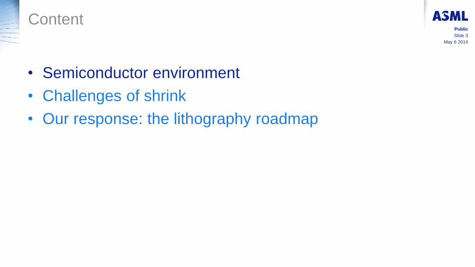
2,294
1,461
627
2,585 2,184
935 1,489
686
570
698
233
366 844
588
440
199
487
358
315
944
1,856
2,279
2,064
145
417
437
421
613
767
930
1,252
367
0
1000
2000
3000
4000
5000
6000
2007 2008 2009 2010 2011 2012 2013 2014
Net S
ale
s
ASML total net sales M€ by End-use May 6 2014
Public
Slide 4
3,768
Numbers have been rounded for readers’ convenience
2,954
1,596
4,508
5,651
Memory
IDM
Foundry
Service & Options
4,732
5,245
YTD

Business environment for 2014
• Bit growth forecast mid 40s% driven by SSD drives and smartphones
• Demand being met through shrink and capacity expansion
• Challenges in qualification of vertical NAND and future node planar
technologies, creating litho demand timing uncertainty
• Bit growth forecast of 20 - 30%
• Bits supplied by planned technology transitions meet bit demand forecast
• Litho process intensity increases due to node transition and mobile DRAM
process complexity
May 6 2014
Public
Slide 5
• Customers are installing capacity for their 20/16/14 nm nodes
• Timing uncertainty in next generation device designs and production ramps

Longer term Logic growth is in Mobile Creating Logic market share battles
May 6 2014
Slide 6
Public
Source: Bob Johnson,Gartner, ISS, Jan 2014
Mobile
Market growth
2011-2017
Premium Smartphone
Basic Smartphone
Traditional Mobile Phone
Premium tablet
Basic Tablet
PC. Ultra Mobile
PC. Notebook
PC. Desktop
2011 2013 2015 2017 2012 2014 2016
140
120
100
80
60
40
20
0
160
Semiconductor Sales
$B
+60%
Semi Mobile/PC
+400% Traditional
-20%
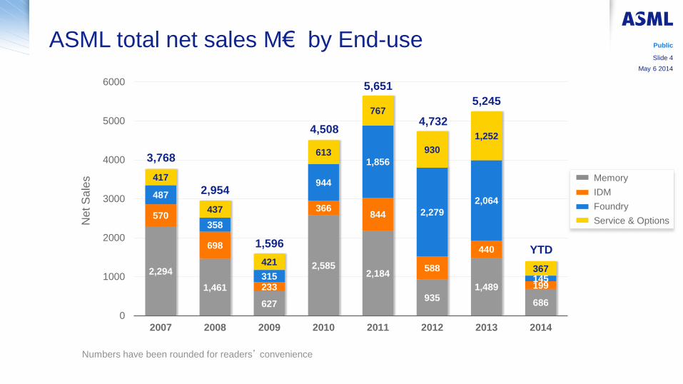
Low power starts to drive the technology roadmap
Source: Geoffrey Yeap, Qualcomm, IEDM, Dec 2013
65 nm/ 45 nm
28 nm
Computing
Wireless
Consumer, Other
T = 0
T = 0
Mobile Computing
28nm Low
Power
28nm high performance mobile
May 6 2014
Public
Slide 7

Source: IHS Electronics & Media, January 2014
The Smartphone boom Foundries and fabless drive the logic market
May 6 2014
Public
Slide 8

Content
May 6 2014
Slide 9
• Semiconductor environment
• Challenges of shrink
• Our response: the lithography roadmap
Public

No end in sight for logic scaling
N20 N20 / N14 N1x / N7 N7 / N5 N5 / N3.5
SOI: Silicon on Insulator
Bulk FinFet : Fin field effect
transistor
SOI FinFet : Silicon on insulator
fin field effect
transistor, III-V
Gate-all-around
transistor
Bulk CMOS: Complementary
Metal Oxide
Semiconductor
May 6 2014
Public
Slide 10
Bulk CMOS:100nm gate length
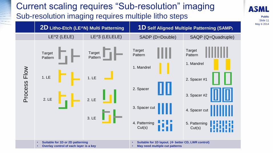
Current scaling requires “Sub-resolution” imaging Sub-resolution imaging requires multiple litho steps
2D Litho-Etch (LE^N) Multi Patterning 1D Self Aligned Multiple Patterning (SAMP)
• Suitable for 1D or 2D patterning
• Overlay control of each layer is a key
• Suitable for 1D layout. ( better CD, LWR control)
• May need multiple cut patterns
LE^2 (LELE) LE^3 (LELELE) SADP (D=Double) SAQP (Q=Quadruple)
1. Mandrel
2. Spacer
3. Spacer cut
Pro
cess F
low
1. LE
2. LE
Target
Pattern
Target
Pattern Target
Pattern
Target
Pattern
2. LE
1. LE
3. LE
1. Mandrel
2. Spacer #1
3. Spacer #2
4. Spacer cut
5. Patterning
Cut(s)
4. Patterning
Cut(s)
May 6 2014
Public
Slide 11

Content Slide 12
• Semiconductor environment
• Challenges of shrink
• Our response: the litho roadmap
Public
May 6 2014

Our Challenge: enable affordable scaling Slide 13
• Scaling needs to create lower cost and
improved performance – ie., support Moore’s Law
• Affordable scaling in lithography can be achieved:
• In the near term - Immersion: drive productivity and yield
(overlay and focus control) with multiple patterning using
advanced litho equipment extended with application
products - Holistic Lithography/Yieldstar
• In the mid/long term - EUV: drive productivity/availability
and improve operational cost
Public
May 6 2014

NXE:3300B, NXE:3350C, …
NXT:1950i, NXT:1960Bi, NXT:1970Ci
Affordable shrink roadmap
May 6 2014
Slide 14
2012 2013 2014 2015 2016 2017
ArF
Dry
KrF
2018 2019 2020
EU
V
Imm
ers
ion
DCO 2.5 nm <1.0 nm
CDU 2.0 nm 0.6 nm
Throughput 230 wafers per hour (wph) >250 wph
Resolution 27 nm 7 nm
EUV to immersion overlay 7.0 nm 1.7 nm
Throughput 50 wph >125 wph
XT:1460,1060,860
Overlay main driver in logic/foundry (ArF with 1460K system
and KrF with 1060K system)
Extend the productivity on the non critical KrF (XT:860L/800-
3D): memory applications
Supported by a Holistic
Lithography approach using
computational litho, overlay
and CD metrology, feedback
loops for wider process
window creation and process
control
Public
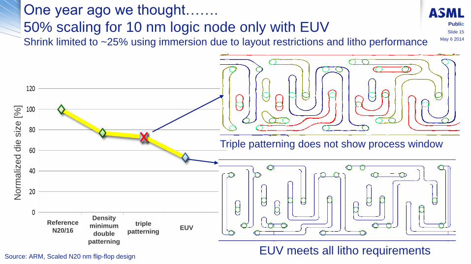
One year ago we thought…….
50% scaling for 10 nm logic node only with EUV Shrink limited to ~25% using immersion due to layout restrictions and litho performance
Reference
N20/16
Density
minimum
double
patterning
triple
patterning EUV
No
rma
lize
d d
ie s
ize
[%
]
Source: ARM, Scaled N20 nm flip-flop design EUV meets all litho requirements
Triple patterning does not show process window
Slide 15
Public
May 6 2014

One year ago we thought…….
50% scaling for 10 nm logic node only with EUV Shrink limited to ~25% using immersion due to layout restrictions and litho performance
EUV 2D metal structure
Single layer solution
ArFi 2D metal structure
3-4 exposures, single layer
insufficient patterning fidelity
Slide 16
Public
May 6 2014
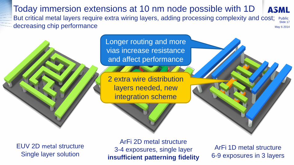
Today immersion extensions at 10 nm node possible with 1D But critical metal layers require extra wiring layers, adding processing complexity and cost;
decreasing chip performance
EUV 2D metal structure
Single layer solution ArFi 1D metal structure
6-9 exposures in 3 layers
ArFi 2D metal structure
3-4 exposures, single layer
insufficient patterning fidelity
Longer routing and more
vias increase resistance
and affect performance
2 extra wire distribution
layers needed, new
integration scheme
Slide 17
Public
May 6 2014

10nm logic design can be done in 1D design w/ immersion
But at the cost of 15% larger dies at comparable design rules May 6 2014
Public
Slide 18
2D
Die Size: 100%
1D
Die Size: 115%
EUV Immersion multi-pass
patterning

0.1
1
40 nm 28 nm 20/16 nm 10 nm 7 nm 5 nm
Critical metal cost/immersion
Patterning cost per flop/immersion
Moore's law
Patte
rnin
g c
ost
norm
aliz
ed to N
20/N
16
Cost: 1D/immersion vs 2D/EUV
Critical metal 1D density
requires extra layers, results in
steep cost increase
Shrink is possible with 1D
designs using immersion, but
cost reduction slows
May 6 2014
Slide 19
Public
The flip flop is a basic
building block of
sequential logic
circuits.

0.1
1
40 nm 28 nm 20/16 nm 10 nm 7 nm 5 nm
Critical metal cost/immersion
Critical metal cost/EUV
Patterning cost per flop/immersion
Patterning cost per flop/EUV
Moore's law
Cost: 1D/immersion vs 2D/EUV
Staying with 2D designs using EUV at N10
is more cost-effective, but risk mitigation
may force 1D design with multiple patterning
Patte
rnin
g c
ost
norm
aliz
ed to N
20/N
16
2D EUV: critical
metal cost
dramatically
reduced
May 6 2014
Slide 20
Public
The flip flop is a basic
building block of
sequential logic
circuits.

EUV: Evaluations for 10nm process insertion underway May 6 2014
Public
Slide 21
Large vacuum
chamber
Mirror optics
New light
source

EUV – progress toward production insertion
• Customers are qualifying EUV for insertion at the 10 nm logic node
• For process development, customers typically require 100 wafers per day,
increasing to 500 wafers per day on average for production qualification
• We have provided customers with process development capability
• In 2016 we will provide our customers with the productivity needed for
volume production, 1500wpd -> 2000wpd
• Our target is to recognize a total of 8 EUV systems in revenue this year
May 6 2014
Public
Slide 22

NXE:3100 in use for cycles of learning at customers 6 systems operational at customers for multiple years
Ac
cu
mu
late
d w
afe
rs e
xp
os
ed
on
NX
E:3
10
0
0
10000
20000
30000
40000
50000
60000
70000
80000
20
10
26
20
10
32
20
10
38
20
10
44
20
10
50
20
11
04
20
11
10
20
11
16
20
11
22
20
11
28
20
11
34
20
11
40
20
11
46
20
11
52
20
12
06
20
12
12
20
12
18
20
12
24
20
12
30
20
12
36
20
12
42
20
12
48
20
13
02
20
13
08
20
13
14
20
13
20
20
13
26
20
13
32
20
13
38
20
13
44
20
13
50
20
14
04
Slide 23
Public
May 6 2014

NXE:3100 shows stable performance and is used for
device development at customer sites
Data courtesy of TSMC and imec – EUVL Toyama 2013
Slide 24
Public
May 6 2014

Full wafer CDU = 1.5nm
22nm HP
BE = 15.9 mJ/cm2
EL = 13% DoF = 160 nm
13 nm HP (Inpria) 9 nm HP
EUV Spacer
NXE:3300B Excellent single exposure imaging performance
16 nm HP (CAR)
22nm 31nm 17nm
2D Contact
10nm Metal 1
Tip-Line, Tip-Tip
1D line spaces
Slide 25
Public
May 6 2014
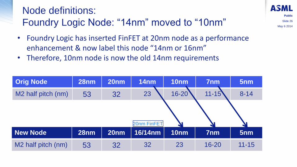
Node definitions:
Foundry Logic Node: “14nm” moved to “10nm” Public
Slide 26
• Foundry Logic has inserted FinFET at 20nm node as a performance enhancement & now label this node “14nm or 16nm”
• Therefore, 10nm node is now the old 14nm requirements
New Node 28nm 20nm 16/14nm 10nm 7nm 5nm
M2 half pitch (nm) 53 32 32 23 16-20 11-15
Orig Node 28nm 20nm 14nm 10nm 7nm 5nm
M2 half pitch (nm) 53 32 23 16-20 11-15 8-14
20nm FinFET
May 6 2014

NXE:3300B showing excellent matched machine overlay
performance on multiple systems to immersion
Systems
Mat
ched
Mac
hin
e
Ove
rlay
[n
m]
0
0.5
1
1.5
2
2.5
3
3.5
4
4.5
5
1 2 3 4
Overlay X Overlay Y
Slide 27
Public
May 6 2014

EUV meets aggressive 2D logic imaging requirements
0
10
20
30
40
50
60
70
80
20 nm 16 nm 10 nm 7 nm
CD
[n
m]
CD requirements by node
Tip-to-tip Tip-to-line Lines and spaces
31nm
22nm
16nm
* using high dose resist @ ~50mJ
EUV (SE)* Slide 28
Public
May 6 2014

• Multiple NXE:3300B systems fully qualified
• 2 systems exposing wafers at the customer sites
• 3 systems under install
EUV (NXE:33x0B) system status overview
• 6 more NXE:3300B systems being integrated
• First NXE:3350B system has been started
• EUV cleanroom extension is under construction
Slide 29
Public
May 6 2014

Under study
Resolution [nm] 32 27 22 16 13 10 7 <7
layo
ut NA 0.25 0.33
13.5
Lens flare 8% 6% 4%
Illumination Flex-OAI s=0.8 Extended Flex-OAI
reduced pupil fill ratio
0.33NA DPT
s=0.5 s=0.2-0.9 coherence
Wavelength [nm]
4.0 7 3.0 DCO [nm]
MMO [nm] 7.0 - 5.0
1.2 1.5 1.0
2.0 2.5 1.7
pupil fill ratio defined as the
bright fraction of the pupil
Overlay
10 5 15 Dose [mJ/cm2]
Power [W] 10 - 105 3 80 - 250
20 20
250 250 TPT (300mm)
Throughphut [w/hr] 6 - 60 - 50 - 125 125 125
20
500
165
NXE technology roadmap - extendibility to <7nm (half pitch)
>0.5NA
Slide 30
Public
Half pitch
May 6 2014

EUV results summary and status Slide 31 Summary
• NXE:3300B operational and exposing wafers at customer sites
• Performance fit for customer development 10nm Logic (and sub-20nm DRAM) and beyond
Status
1. EUV lithography technology is proven and is entering the industrialization phase
2. The EUV qualification requires 100 wafer per day output, which is determined by:
a) Power: Supporting 30 wafers per hour
b) Availability: Of greater than 50%
3. For pre-production customers have asked us to deliver 500 wafers per day by the end of 2014.
4. The full market potential of EUV will be realized at 125 wafers per hour and system availability >
90%. This will happen as a result of series of stepped through-put and reliability/availability
upgrades.
5. The value of EUV is undisputed as the lithographic shrink technology of choice for multiple nodes
starting in 2016/2017.
6. Our customers and peers continue to support and drive development of EUV systems and
infrastructure for introduction of EUV into volume production in the stated timeframe.
Public
May 6 2014