Embed Size (px)
Citation preview

*
EUROPEAN ETS 300 394-1
TELECOMMUNICATION March 1996
STANDARD
Source: ETSI TC-RES Reference: DE/RES-06009-1
ICS: 33.020, 30.060.50
Key words: TETRA, radio conformance testing
Radio Equipment and Systems (RES);Trans-European Trunked Radio (TETRA);
Conformance testing specification;Part 1: Radio
ETSIEuropean Telecommunications Standards Institute
ETSI Secretariat
Postal address: F-06921 Sophia Antipolis CEDEX - FRANCEOffice address: 650 Route des Lucioles - Sophia Antipolis - Valbonne - FRANCEX.400: c=fr, a=atlas, p=etsi, s=secretariat - Internet: [email protected]
Tel.: +33 92 94 42 00 - Fax: +33 93 65 47 16
Copyright Notification: No part may be reproduced except as authorized by written permission. The copyright and theforegoing restriction extend to reproduction in all media.
© European Telecommunications Standards Institute 1996. All rights reserved.

Page 2ETS 300 394-1: March 1996
Whilst every care has been taken in the preparation and publication of this document, errors in content,typographical or otherwise, may occur. If you have comments concerning its accuracy, please write to"ETSI Editing and Committee Support Dept." at the address shown on the title page.

Page 3ETS 300 394-1: March 1996
Contents
Foreword .......................................................................................................................................................7
1 Scope ..................................................................................................................................................9
2 Normative references..........................................................................................................................9
3 Definitions, symbols and abbreviations ...............................................................................................93.1 Definitions ............................................................................................................................93.2 Symbols .............................................................................................................................103.3 Abbreviations .....................................................................................................................10
4 General..............................................................................................................................................104.1 Presentation of equipment for testing purposes ................................................................10
4.1.1 Facilities and information required for testing ...............................................104.1.2 Choice of radio frequency channels to be tested ..........................................114.1.3 Interpretation of the measurement results ....................................................11
4.2 Mechanical and electrical design .......................................................................................114.2.1 General..........................................................................................................114.2.2 Controls .........................................................................................................124.2.3 Marking..........................................................................................................12
5 Radio test configuration, test signals and test modes.......................................................................125.1 General functional radio test configuration ........................................................................125.2 Radio test modes...............................................................................................................12
5.2.1 Test receive mode.........................................................................................135.2.1.1 MS test receive mode..........................................................135.2.1.2 BS test receive mode ..........................................................13
5.2.2 Test transmit mode .......................................................................................145.2.2.1 MS V+D testing....................................................................145.2.2.2 MS PDO testing ...................................................................145.2.2.3 BS V+D & PDO testing ........................................................14
5.3 Radio test signals...............................................................................................................155.3.1 General..........................................................................................................155.3.2 Test signal T1 (TETRA wanted signal) .........................................................15
5.3.2.1 MS V+D testing....................................................................155.3.2.2 BS V+D testing ....................................................................165.3.2.3 MS PDO testing ...................................................................175.3.2.4 BS PDO testing....................................................................17
5.3.3 Test signal T2 (TETRA interferer) .................................................................175.3.4 Test signal T3 (un-modulated interferer).......................................................17
6 Test conditions ..................................................................................................................................186.1 General ..............................................................................................................................186.2 Power sources and ambient temperatures........................................................................18
6.2.1 Normal test conditions...................................................................................186.2.2 Extreme test conditions.................................................................................18
6.3 Procedure for tests at extreme temperatures ....................................................................196.3.1 Equipment designed for continuous operation..............................................196.3.2 Equipment designed for intermittent operation .............................................20
7 Technical characteristics...................................................................................................................207.1 Transmitter parameter definitions & limits .........................................................................20
7.1.1 Transmitter output power ..............................................................................207.1.1.1 Definition..............................................................................207.1.1.2 Limit values..........................................................................20
7.1.2 Unwanted output power in non-active transmit state ....................................217.1.2.1 Definition..............................................................................21

Page 4ETS 300 394-1: March 1996
7.1.2.2 Limit values ......................................................................... 217.1.3 Adjacent channel power due to modulation.................................................. 21
7.1.3.1 Definition ............................................................................. 217.1.3.2 Limit values ......................................................................... 21
7.1.4 Adjacent channel power due to switching transients .................................... 217.1.4.1 Definition ............................................................................. 217.1.4.2 Limit values ......................................................................... 21
7.1.5 Unwanted emissions far from the carrier...................................................... 227.1.5.1 Definition ............................................................................. 227.1.5.2 Limit values ......................................................................... 22
7.1.6 Unwanted radiated emissions....................................................................... 227.1.6.1 Definition ............................................................................. 227.1.6.2 Limit values ......................................................................... 22
7.1.7 Unwanted emissions during the BLCH/CLCH (linearization)........................ 227.1.7.1 Definition ............................................................................. 227.1.7.2 Limit values ......................................................................... 23
7.1.8 Intermodulation attenuation .......................................................................... 237.1.8.1 Definition ............................................................................. 237.1.8.2 Limit values ......................................................................... 23
7.1.8.2.1 MS Limit values.................................... 237.1.8.2.2 Limit values for single BS transmitter... 237.1.8.2.3 Limit values for Intra BS
intermodulation..................................... 237.2 Receiver parameter definitions and limits ......................................................................... 24
7.2.1 General ......................................................................................................... 247.2.2 Nominal error rates....................................................................................... 24
7.2.2.1 Definition ............................................................................. 247.2.2.2 Limit values ......................................................................... 24
7.2.3 Reference sensitivity performance ............................................................... 247.2.3.1 Definition ............................................................................. 247.2.3.2 Limit values ......................................................................... 25
7.2.4 Reference interference performance............................................................ 257.2.4.1 Definition ............................................................................. 257.2.4.2 Limit values ......................................................................... 25
7.2.5 Blocking characteristics ................................................................................ 267.2.5.1 Definition ............................................................................. 267.2.5.2 Limit values ......................................................................... 26
7.2.6 Spurious response rejection ......................................................................... 267.2.6.1 Definition ............................................................................. 267.2.6.2 Limit values ......................................................................... 26
7.2.7 Intermodulation response rejection .............................................................. 277.2.7.1 Definition ............................................................................. 277.2.7.2 Limit values ......................................................................... 27
7.2.8 Unwanted conducted emissions................................................................... 277.2.8.1 Definition ............................................................................. 277.2.8.2 Limit values ......................................................................... 27
7.2.9 Unwanted radiated emissions....................................................................... 277.2.9.1 Definition ............................................................................. 277.2.9.2 Limit values ......................................................................... 27
7.3 Transmitter / receiver parameter definitions & limits......................................................... 277.3.1 Modulation accuracy..................................................................................... 27
7.3.1.1 Definition ............................................................................. 277.3.1.2 Limit values ......................................................................... 28
7.3.2 Carrier frequency accuracy........................................................................... 287.3.2.1 Definition ............................................................................. 287.3.2.2 Limit values ......................................................................... 28
7.3.3 MS receiver performance for synchronization burst acquisition ................... 287.3.3.1 Definition ............................................................................. 287.3.3.2 Limit values ......................................................................... 28
7.3.4 MS Frame alignment performance............................................................... 287.3.4.1 Definition ............................................................................. 287.3.4.2 Limit values ......................................................................... 28
7.3.5 MS link control .............................................................................................. 29

Page 5ETS 300 394-1: March 1996
7.3.5.1 Definition..............................................................................297.3.5.2 Limit values..........................................................................29
8 Methods of measurement for transmitter parameters.......................................................................298.1 Transmitter output power...................................................................................................29
8.1.1 MS transmitter output power .........................................................................308.1.2 BS transmitter output power..........................................................................30
8.2 Unwanted output power in non active transmit state .........................................................318.3 Adjacent channel power due to modulation.......................................................................318.4 Adjacent channel power due to switching transients .........................................................328.5 Unwanted emissions far from the carrier...........................................................................328.6 Unwanted radiated emissions............................................................................................328.7 Unwanted emissions during the BLCH/CLCH (linearization).............................................338.8 Intermodulation attenuation ...............................................................................................33
8.8.1 MS Intermodulation attenuation ....................................................................338.8.2 BS Intermodulation attenuation .....................................................................338.8.3 Intra BS intermodulation................................................................................33
9 Methods of measurement for receiver parameters ...........................................................................349.1 General ..............................................................................................................................349.2 Nominal error rates ............................................................................................................34
9.2.1 MS nominal error rate....................................................................................349.2.2 BS nominal error rate ....................................................................................34
9.3 Reference sensitivity performance ....................................................................................349.3.1 MS reference sensitivity performance...........................................................359.3.2 BS reference sensitivity performance............................................................359.3.3 PUEM performance.......................................................................................35
9.4 Reference interference performance.................................................................................359.4.1 MS reference interference performance .......................................................369.4.2 BS reference interference performance........................................................36
9.5 Blocking characteristics .....................................................................................................369.5.1 MS blocking...................................................................................................379.5.2 BS blocking ...................................................................................................37
9.6 Spurious response rejection ..............................................................................................379.7 Intermodulation response rejection....................................................................................37
9.7.1 MS intermodulation response rejection.........................................................379.7.2 BS intermodulation response rejection..........................................................38
9.8 Unwanted emissions..........................................................................................................38
10 Methods of measurement for transmitter/receiver parameters.........................................................3810.1 Modulation accuracy ..........................................................................................................38
10.1.1 MS modulation accuracy ...............................................................................3810.1.2 BS modulation accuracy................................................................................3910.1.3 Vector error magnitude at symbol time .........................................................39
10.2 Carrier frequency accuracy................................................................................................3910.2.1 MS carrier frequency accuracy......................................................................3910.2.2 BS carrier frequency accuracy ......................................................................40
10.3 MS receiver performance for synchronization burst acquisition ........................................4010.4 MS Frame alignment performance ....................................................................................4010.5 MS link control ...................................................................................................................41
11 Measurement uncertainty..................................................................................................................42
Annex A (normative): TETRA receiver testing ......................................................................................43
A.1 Frequencies of spurious response ....................................................................................................43A.1.1 Spurious response rejection ..............................................................................................43
A.1.1.1 Definition .......................................................................................................43A.1.1.2 Introduction to the method of measurement .................................................43
A.2 Test cases and test conditions for BS and MS receivers..................................................................43
A.3 Test signal T1, content of BSCH and BNCH/T (V+D) & MBCH/T (PDO) .........................................49

Page 6ETS 300 394-1: March 1996
Annex B (normative): Radio test system functions............................................................................... 51
B.1 Test transmitter and receiver............................................................................................................ 51B.1.1 General.............................................................................................................................. 51B.1.2 Sampling system............................................................................................................... 51
B.1.2.1 General ......................................................................................................... 51B.1.2.2 TETRA filter .................................................................................................. 51B.1.2.3 Adjacent channel power measurements ...................................................... 51B.1.2.4 Modulation accuracy measurements............................................................ 52B.1.2.5 Measurement of unwanted output power in the non-active transmit state ... 52
B.1.3 Spectrum analyzer ............................................................................................................ 52B.1.4 Error rate tester ................................................................................................................. 52B.1.5 Interfering signal sources .................................................................................................. 52B.1.6 Propagation simulators ..................................................................................................... 53B.1.7 Timing measurement unit ................................................................................................. 53B.1.8 Passive test system components...................................................................................... 53B.1.9 Test system controller ....................................................................................................... 53B.1.10 Test signal (T1, T2) requirements..................................................................................... 53
B.1.10.1 Adjacent channel power ............................................................................... 53B.1.10.2 Modulation accuracy..................................................................................... 54
History ......................................................................................................................................................... 55

Page 7ETS 300 394-1: March 1996
Foreword
This European Telecommunication Standard (ETS) has been produced by the Radio Equipment andSystems (RES) Technical Committee of the European Telecommunications Standards Institute (ETSI).
Every ETS prepared by ETSI is a voluntary standard. This ETS contains text concerning conformancetesting of the equipment to which it relates. This text should be considered only as guidance and does notmake this ETS mandatory.
This ETS will consist of three parts:
Part 1: "Radio".
Part 2: "Protocol testing specification (V+D)", (DE/RES-06009-2).
Part 3: "Protocol testing specification (PDO)", (DE/RES-06009-3).
Transposition dates
Date of adoption of this ETS: 12 January 1996
Date of latest announcement of this ETS (doa): 31 May 1996
Date of latest publication of new National Standardor endorsement of this ETS (dop/e): 30 November 1996
Date of withdrawal of any conflicting National Standard (dow): 30 November 1996

Page 8ETS 300 394-1: March 1996
Blank page

Page 9ETS 300 394-1: March 1996
1 Scope
This ETS specifies the minimum technical characteristics of both TETRA Voice plus Data (V+D) andPacket Data Optimised (PDO) Base Stations (BS) and Mobile Station (MS) equipment and the radio testmethods used for type testing. The purpose of these specifications is to provide a sufficient quality of radiotransmission and reception for equipment operating in a TETRA system and to minimise harmfulinterference to other equipment. The document is applicable to TETRA systems operating at radiofrequencies in the range of 380 MHz to 520 MHz.
These specifications do not necessarily include all the characteristics which may be required by a user ofequipment, nor do they necessarily represent the optimum performance achievable.
2 Normative references
This ETS incorporates by dated and undated reference, provisions from other publications. Thesenormative references are cited at the appropriate places in the text and the publications are listedhereafter. For dated references, subsequent amendments to or revisions of any of these publicationsapply to this ETS only when incorporated in it by amendment or revision. For undated references the latestedition of the publication referred to applies.
[1] ETS 300 392-2: "Radio Equipment and Systems (RES); Trans-EuropeanTrunked Radio (TETRA); Voice plus Data (V+D); Part 2: Air Interface (AI)".
[2] ETS 300 393-2: "Radio Equipment and Systems (RES); Trans-EuropeanTrunked Radio (TETRA); Packet Data Optimized (PDO); Part 2: Air Interface(AI)".
[3] CCITT Recommendation O.153: "Basic parameters for the measurement oferror performance at bit rate below the primary rate".
[4] ETR 028: “Radio Equipment and Systems (RES); Uncertainties in themeasurement of mobile radio equipment characteristics”.
[5] ETS 300 113: " Radio Equipment and Systems (RES); Land mobile service;Technical characteristics and test conditions for radio equipment intended forthe transmission of data (and speech) and having an antenna connector".
3 Definitions, symbols and abbreviations
3.1 Definitions
For the purposes of this standard, the following definitions apply:
Refer to ETS 300 392-2 [1], clause 3 for common definitions.
accreditation body: The body that conducts and administers a laboratory accreditation system andgrants accreditation.
receive band of the equipment: The maximum frequency range (declared by the manufacturer) overwhich the receiver can be operated without reprogramming or realignment.
accredited laboratory: Testing laboratory to which accreditation has been granted.
testing laboratory: A laboratory that performs tests.
transmit band of equipment: The maximum frequency range (declared by the manufacturer) over whichthe transmitter can be operated without reprogramming or realignment.

Page 10ETS 300 394-1: March 1996
3.2 Symbols
For the purposes of this ETS, the following symbols apply:
flo local oscillator frequency applied to first receiver mixerfo nominal centre frequency of radio channelif1...ifn receiver intermediate frequenciesPMS access powerPTx MS transmit powerRlev averaged signal level received by MS
3.3 Abbreviations
For the purposes of this ETS, the following abbreviations apply:
Refer to ETS 300 392-2 [1], clause 3 for common abbreviations.
B Measurement bandwidthBER Bit Error RatioC/I Carrier to Interference ratiodBc Decibels relative to carrier powerdBm Decibels relative to one mWMER Message Erasure RatePACQ Probability of synchronization burst ACQuisitionPRBS Pseudo Random Bit SequencePUEM Probability of Undetected Erroneous MessageRF Radio FrequencyRMS Root Mean SquareRx ReceiverSB Synchronization BurstTx TransmitterVSWR Voltage Standing Wave Ratio
4 General
4.1 Presentation of equipment for testing purposes
Each equipment submitted for type testing shall fulfil the requirements of this standard on all channelsover which it is intended to operate. The manufacturer, or other applicant, shall provide one or moreproduction model(s) of the equipment, as appropriate, for type testing. If type approval is given on thebasis of tests on pre-production models, those models shall be manufactured in accordance with thesame production drawings and manufacturers specifications as the later production models. This factshall be declared by the manufacturer in the application form. For more details refer to ETS 300 113 [5].
4.1.1 Facilities and information required for testing
The applicant shall, when submitting equipment for type testing, provide the following facilities:
- at least one antenna connector as a test point;
- for equipment supporting diversity, or for any other reason having more than one antennaconnector, the applicant shall supply coupling and/or terminating devices so that the tests can beperformed via a single antenna connector;
- TETRA equipment, for example PDO radio packet modem modules which may not have anantenna connector, may be submitted for type testing by the manufacturer, or other applicant, if asuitable jig or adapter is supplied which allows the conducted tests to be carried out;
- specific test modes, as defined in subclause 5.2;

Page 11ETS 300 394-1: March 1996
- a test connector which provides decoded data output for all uplink logical channels in the case ofBS and downlink logical channels in the case of MS to be tested. The test connector shall alsoprovide any test signalling data;
- a means to connect the equipment to the test power source according to clause 6.
The applicant shall provide the following information to the test laboratory:
- power class of equipment;
- receiver class A, B or E (MS only);
- other capabilities and options implemented in equipment, including V+D or PDO, traffic channelssupported;
- information related to radio sub-system of equipment, i.e. transmit and receive frequency bands,first local oscillator frequency (flo) and intermediate frequencies (if1...ifn) of receiver;
- description how to use equipment in specific test modes and test connector interface details;
- information of power source used in equipment.
4.1.2 Choice of radio frequency channels to be tested
Unless otherwise stated, the tests described in clauses 8, 9 and 10 shall be performed on the lowest,highest and middle radio frequency channel of either the transmit or receive band of the equipment,whichever is appropriate.
4.1.3 Interpretation of the measurement results
The interpretation of the results recorded in the test report for the measurements described in thisstandard shall be as follows:
a) the measured value related to the corresponding limit will be used to decide whether an equipmentmeets the minimum requirements of the specification in accordance with the shared risk method;
b) the actual measurement uncertainty of the test laboratory carrying out the measurement, for eachparticular measurement, shall be included in the test report;
c) the values of the actual measurement uncertainty shall be, for each measurement, equal to or lowerthan the figures given in clause 11. The measurement uncertainty requirements given in thisspecification corresponds to a confidence level of 95 %, unless otherwise stated. The confidencelevel is the probability that the true value of the measured parameter lies within the range of valuesbounded by the uncertainty as described in ETR 028 [4].
This procedure for using maximum acceptable uncertainty values is valid until superseded by otherappropriate ETSI publications covering this subject. The use of the measured value has been chosenbecause there is no definitive standard allowing for measurement uncertainty at the time of publication ofthis standard. Therefore, the measurement uncertainty shall be used to assess the quality of the actualmeasurement. The measurement uncertainty values can also be used by accreditation authorities duringtheir accreditation procedures to ensure compliance of type testing to ETSI standards.
4.2 Mechanical and electrical design
4.2.1 General
The equipment submitted for type testing by the manufacturer or other applicant, shall be designed,constructed and manufactured in accordance with sound engineering practice and with the aim tominimise harmful interference to other equipment and services.

Page 12ETS 300 394-1: March 1996
4.2.2 Controls
Those controls which if maladjusted might increase the interfering potentialities of the equipment shall notbe accessible to the user.
4.2.3 Marking
The equipment shall be marked in a visible place. This marking shall be legible, tamperproof and durable.
The marking shall include:
- the name of the manufacturer or his trade mark;
- type number of designation and serial number;
- type approval number (when allocated by appropriate authorities).
5 Radio test configuration, test signals and test modes
This clause outlines, in terms of functional blocks, the test system required to perform the radio testprocedures and test modes used in clauses 8, 9 and 10.
5.1 General functional radio test configuration
The radio test system configuration shown in figure 1 is presented for information only and is notmandatory. The equipment under test shall be connected to the test system via the antenna connector.The tasks and characteristics of the test system functional blocks are described in annex B, clause B.1.All power level and frequency characteristics specified shall be, unless otherwise stated, referred to theantenna connector of the equipment under test.
RF signalgenerator
RF signalgenerator
propagationsimulator
(test transceiver)
testererror rate
timingmeas.
samplingsystem
spectrumanalyzer
propagationsimulator
splitter
combiner
wanted signal
isolatingdevice
MS under test
MS antennaconnector
Testconnector
Test transmit
BusinterfaceTest
System
Controller
Tx
2nd Interferer
1st Interferer
Figure 1: Radio test configuration
5.2 Radio test modes
The manufacturer shall provide the means to operate the equipment under test in either test transmit ortest receive modes. The MS under test shall be instructed which test mode to operate in using the Tx_onparameter contained in the BNCH/T(V+D) or MBCH/T(PDO) channels of test signal T1 transmitted by thetest system. Further details of test signal T1 and the contents of BNCH/T and MBCH/T are found insubclause 5.3.2 and annex A, clause A.3. For a BS under test the manufacturer shall provide the meansto configure the BS operation for all type tests to be conducted.

Page 13ETS 300 394-1: March 1996
5.2.1 Test receive mode
5.2.1.1 MS test receive mode
In test receive mode the MS under test shall provide at the test connector a decoded data output for eachdownlink logical channel (control, traffic) to be tested. The logical channel type to be decoded is indicatedusing the T1_burst_type parameter in the BNCH/T(V+D) or MBCH/T(PDO).
In all cases whenever the MS decodes a timeslot containing BSCH and BNCH/T(V+D) or MBCH/T(PDO)the MS shall provide the data decoded from these channels at the test connector. In the case where theMS detects an erroneous message on the BSCH, BNCH/T(V+D) or MBCH(PDO) transmitted by the testequipment during frame 18, the MS shall remain in the same state as it was on frames 1 to 17.
5.2.1.2 BS test receive mode
Using the method provided by the manufacturer, the BS in test receive mode shall be configured toreceive the desired logical channel type from the test system. The BS shall operate in its normal modeand provide at the test connector the decoded data output of each uplink logical channel tested.
A V+D BS shall be configured to receive the desired logical channel on timeslot 1 of each uplink frame.During testing the test system shall use the down link BS transmissions to synchronise its uplink burstfrequency and timing. The BS shall transmit in timeslot 1 of frame 18 a downlink synchronization burstaccording to table 1.
Table 1: Base Station down link synchronization burst
Burst type Block 1 Block 2 Broadcast Blocksynchronization BSCH BNCH/T AACH
The downlink synchronization burst contains both BSCH and BNCH/T channels, which includes theT1_burst_type parameter indicating the logical channel the BS is expecting to receive. The BNCH/T is alogical channel specific to the test mode. The contents of the BSCH and BNCH/T channels used duringtesting are defined in annex A, clause A.3. For a V+D BS in continuous mode time slots 1 to 4 of downlinkframes 1 to 17 and time slots 2 to 4 of downlink frame 18 are filled with a channel type 1 signal, seesubclause 5.3.2 for details of channel types. For a V+D BS in discontinuous mode time slot 1 of downlinkframes 1 to 17 are filled with a channel type 1 signal.
Unless otherwise specified the following configuration shall be used:
- channel type 1 (see subclause 5.3.2 for details);
- the parameters MS_TXPWR_MAX_CELL shall be set to 15 dBm;
- the parameter ACCESS_PARAMETER shall be set to - 53 dBm.
A PDO BS shall transmit in sub burst 1 a down link synchronization burst according to table 2.
Table 2: Sub burst type
Sub burst typesynchronization MBCH/T
The downlink synchronization burst shall be used by the test system to synchronise its uplink sub burstfrequency and timing.
The MBCH/T is a logical channel specific to the test mode. The contents of the MBCH/T used duringtesting are defined in annex A, clause A.3. On down link sub bursts 2 to 150 a channel type 6 signal shallbe sent by the BS under test.

Page 14ETS 300 394-1: March 1996
Unless otherwise specified the following configuration shall be used:
- channel type 6;
- start of reservation value 30 (equivalent to 240 symbol durations);
- the parameters MS_TXPWR_MAX_CELL shall be set to 15 dBm;
- the parameter ACCESS_PARAMETER shall be set to - 53 dBm.
In the case of testing a receive-only BS, the manufacturer shall also provide a BS transmitter and therequired interconnections with the receive-only BS for synchronization purposes.
5.2.2 Test transmit mode
5.2.2.1 MS V+D testing
In test transmit mode the MS under test shall transmit either a normal uplink burst or control uplink burst,as indicated by the Tx_Burst_type parameter of the BNCH/T. The MS shall be synchronised in time andfrequency to the test signal T1 and shall transmit only on timeslot 1.
In test transmit mode the MS shall begin by transmitting a typical CLCH burst on subslot 1 of frame 18followed by transmission of TCH/7,2 normal uplink bursts on frames 1 to 17 or SCH/HU control uplinkburst on subslot 1 of frames 1 to 17, the sequence then repeating. Further CLCH opportunities aretherefore available every multiframe. A bit stream, produced by repeating a pseudo random sequence witha length of 511 bits according to CCITT Recommendation O.153 [3], shall be used as the information tobe transmitted over the logical channel. The MS shall set its transmit power according to the measuredsignal strength of signal T1 and the decoded power control parameters in the BNCH/T channel.
In test transmission mode the MS shall continue to monitor the BSCH and BNCH/T transmitted by the testequipment on frame 18.
5.2.2.2 MS PDO testing
In test transmit mode the MS under test shall transmit a sequence of NBCH normal uplink sub bursts. TheMS transmissions shall begin with an uplink start sub burst with normal linearization followed by analternating sequence of uplink even and uplink odd sub bursts. The MS transmission shall be terminatedusing an uplink end sub burst. In test transmit mode the MS transmissions are started and stopped usingthe down link busy flag generated by the test system. A bit stream, produced by repeating a pseudorandom sequence with a length of 511 bits according to CCITT Recommendation O.153 [3], shall be usedas the information to be transmitted over the logical channel.
The MS shall set its transmit power according to the measured signal strength of signal T1 and thedecoded power control parameters in the MBCH/T channel.
5.2.2.3 BS V+D & PDO testing
Using the method provided by the manufacturer, the BS in test transmit mode shall be configured totransmit the desired down link logical channel and burst/sub burst type. The BS shall operate in its normalmode e.g. continuous or discontinuous mode. For a V+D BS in discontinuous mode the BS shall transmitonly in time slot 1 of each frame. A bit stream, produced by repeating a pseudo random sequence with alength of 511 bits according to CCITT Recommendation O.153 [3], shall be used as the information to betransmitted over the logical channel. The BS transmission, if required, shall begin with a BLCH burstfollowed by transmission of desired channel type.

Page 15ETS 300 394-1: March 1996
5.3 Radio test signals
5.3.1 General
In principle the modulation of the test signals T1 and T2, to be described below, shall comply withETS 300 392-2 [1], clause 5. The modulation filter is specified by a set of windowed discrete impulseresponse samples, g'j, where j= 0...N-1 and,
g w g TNj
Nj j s' =
−−
1
1
2
where g(t) is the symbol waveform defined in ETS 300 392-2 [1], clause 5, Ns is the number of symbolsspanned by the filter and T is the symbol duration as defined in ETS 300 392-2 [1], clause 5. Ns shall beat least 15. The window coefficients , wj, are defined by:
( )
( )w
j N
Nj = −
− −
+
1
1
21
1
21
2
The test transmitter shall be sufficiently linear with respect to amplitude and phase (active linearizationshould be avoided whenever possible) to meet the requirements in annex B, clause B.1.
5.3.2 Test signal T1 (TETRA wanted signal)
The T1 signal sequence shall comply with the TETRA (V+D or PDO) air interface multiframe, frame andslot/burst/sub burst structure and is the wanted signal transmitted by the test system during frames 1 to 17in all receiver tests. The information transmitted by the test system in frame 18 of T1 is used for testcontrol purposes. The slot structure of T1 in frames 1 to 17 is dependant upon the type of receiver testbeing conducted, defined by the channel type number.
5.3.2.1 MS V+D testing
During MS V+D receiver testing, the test system shall transmit in timeslot 1 of T1 continuous down linkburst and channel types according to the tables 3 and 4.
On frame 18 according to table 3.
Table 3: Test system transmission
Burst type Block 1 Block 2 Broadcast Blocksynchronization BSCH BNCH/T AACH
The BNCH/T is a logical channel specific to the test mode. The contents of the BSCH and BNCH/T to beused during the test are given in annex A, clause A.3.
On frame 1 to 17 one of the following channel types according to table 4.
Table 4: Channel types
Channel type Burst type Block 1 Block 2 Broadcast Block0 normal TCH/7,2 AACH1 normal TCH/7,2 AACH2 normal SCH/F AACH3 synchronization BSCH SCH/HD AACH4 normal TCH/2,4, N=1 AACH

Page 16ETS 300 394-1: March 1996
A bit stream, produced by repeating a pseudo random sequence with a length of 511 bits according toCCITT Recommendation O.153 [3], shall be used as the information to be transmitted over the logicalchannel.
NOTE: For channel type 3, the logical channels BNCH and STCH have the same coding,interleaving format and performance specification as SCH/HD and are not, therefore,specifically tested.
Channel types 1, 2 and 3 ( in the case of class E equipment only) and 4 shall be tested in continuoustransmission mode where channel type 0 is inserted in time slots 2 to 4 of frames 1 to 18.
Channel type 3 shall in the case of class A and B equipment be tested in continuous transmission modewhere no signal is transmitted on timeslots 2 to 4.
For MS synchronization burst acquisition performance testing, the normal multiframe structure shall not berespected and the synchronization continuous downlink bursts (including start and stop bursts) carryingBSCH/T shall be transmitted randomly. The period between the start of two synchronization bursts shallbe randomly selected in the range between 800 and 25 000 symbol durations, with a step less than orequal to 1/4 symbol duration. Nothing shall be transmitted in the time interval between synchronizationbursts. This special transmission mode is defined as channel type 13.
5.3.2.2 BS V+D testing
During BS V+D receiver testing the test system shall transmit in timeslot 1 of T1 up link burst and channeltypes according to the tables 5 and 6.
On frame 18 according to table 5.
Table 5: Test system transmission
Channel type Burst type Sub slot 1 Sub slot 28 normal SCH/F
On frame 1 to 17 one of the following channel types according to table 6.
Table 6: Channel types
Channel type Burst type Sub slot 1 Sub slot 27 normal TCH/7,28 normal SCH/F9 normal STCH STCH
10 normal TCH/2,4 , N=111 control SCH/HU SCH/HU
For BS receiver testing, channel type 7 shall be inserted in time slots 2 to 4 of all uplink frames 1 to 18. Abit stream, produced by repeating a pseudo random sequence with a length of 511 bits according toCCITT Recommendation O.153 [3], shall be used as the information to be transmitted over the logicalchannel.

Page 17ETS 300 394-1: March 1996
5.3.2.3 MS PDO testing
During MS PDO receiver testing the test system shall transmit T1 down link sub burst and channel typesaccording to the tables 7 and 8.
On sub burst 1 according to table 7.
Table 7: Sub bursts
Channel type Sub burst type5 synchronization MBCH/T
On sub bursts 2 to 150 according to table 8.
Table 8: Sub bursts
Channel type Sub burst type6 normal NBCH
A bit stream, produced by repeating a pseudo random sequence with a length of 511 bits according toCCITT Recommendation O.153 [3], shall be used as the information to be transmitted over the logicalchannel.
For MS synchronization burst acquisition performance testing, the normal sub-burst structure shall not berespected and the synchronization sub-bursts carrying the MBCH/T shall be transmitted randomly asdescribed in subclause 5.3.2.1. This special transmission mode is defined as channel type 14.
5.3.2.4 BS PDO testing
During BS PDO receiver testing the test system shall transmit T1 up link sub burst and channel typesaccording to table 9.
On uplink sub bursts 1 to 150 according to table 9.
Table 9: Sub bursts
Channel type Sub burst type12 normal NBCH
A bit stream, produced by repeating a pseudo random sequence with a length of 511 bits according toCCITT Recommendation O.153 [3], shall be used as the information to be transmitted over the logicalchannel.
5.3.3 Test signal T2 (TETRA interferer)
Test signal T2 is a pi/4 DQPSK modulated continuous radio signal following the structure of TETRAsignals, but with all modulating bits (including training sequences) derived directly from pseudo random bitsequence (with a length of 511 bits according to CCITT Recommendation O.153 [3]).
T2 is used as an unwanted (modulated) signal.
5.3.4 Test signal T3 (un-modulated interferer)
Test signal T3 is an un-modulated continuous sinusoidal radio signal. T3 is used as an unwanted(un-modulated) signal.

Page 18ETS 300 394-1: March 1996
6 Test conditions
6.1 General
Type tests shall be made under normal test conditions and where stated also under extreme testconditions. The test conditions and procedures shall be as specified in subclauses 6.2.1 and 6.2.2.
6.2 Power sources and ambient temperatures
During type tests the power source of the equipment shall be replaced by a test power source, capable ofproducing normal and extreme test voltages as specified in subclauses 6.2.1 and 6.2.2. The internalimpedance of the test power source shall be low enough for its effect on the test results to be negligible.For the purpose of tests, the voltage of the power source shall be measured at the input terminals of theequipment. If the equipment is provided with a permanently connected power cable, the test voltage shallbe that measured at the point of connection of the power cable to the equipment. In equipment withincorporated batteries the test power source shall be applied as close to the battery terminals aspracticable. During tests the power source voltages shall be maintained within a tolerance of ± 1 %relative to the voltage at the beginning of each test.
6.2.1 Normal test conditions
The normal temperature and humidity conditions for tests shall be any convenient combination oftemperature and humidity within the following ranges:
- temperature + 15° C to + 35° C (degrees Celsius);
- relative humidity 20 % to 75 %.
When it is impracticable to carry out the tests under the conditions stated above, the actual temperatureand relative humidity during the tests shall be recorded in the Test Report.
The normal test voltage for equipment to be connected to the mains shall be the nominal mains voltage.For the purpose of these specifications, the nominal voltage shall be the declared voltage or any of thedeclared voltages for which the equipment was designed. The frequency of the test power sourcecorresponding to the mains shall be between 49 Hz and 51 Hz.
When the radio equipment is intended for operation from the usual types of regulated lead-acid batterypower source of vehicles, the normal test voltage shall be 1,1 times the nominal voltage of the battery(6 V, 12 V, etc.).
For operation from other power sources or types of battery (primary or secondary) the normal test voltageshall be that declared by the equipment manufacturer.
6.2.2 Extreme test conditions
For tests at extreme ambient temperatures measurements shall be made at the upper and lowertemperatures of the following range:
- - 20°C to + 55°C.
The extreme test voltages for equipment to be connected to an ac mains source shall be the nominalmains voltage ± 10 %.
When the equipment is intended for operation from the usual types of regulated lead-acid battery powersources of vehicles the extreme test voltages shall be 1,3 and 0,9 times the nominal voltage of the battery(6 V, 12 V, etc.).
Page 19ETS 300 394-1: March 1996
The extreme test voltages for equipment with power sources using non regulated batteries shall be asfollows. The upper extreme test voltage shall be the normal test voltage. The lower extreme test voltageshall be:
- for the Leclanche or the lithium-type of battery, 0,85 times the nominal voltage of the battery;
- for the mercury-type or nickel cadmium type of battery, 0,9 times the nominal voltage of the battery;
- for other types of batteries, end point voltage declared by the equipment manufacturer.
However, the lower extreme test source voltages shall be those agreed between the equipmentmanufacturer and the testing laboratory for the following equipment:
- designed to use other power sources;
- capable of being operated from a variety of power sources;
- designed to include a shut-down facility to ease operation of the equipment at source voltages otherthan those referred to above.
The conditions shall be recorded in the test report and in the latter case the purpose of including thisfacility.
The following four extreme test condition combinations are applied while testing TETRA equipment underextreme test conditions:
- LTLV: - 20 °C and lower voltage;
- LTHV: - 20 °C and higher voltage;
- HTLV: + 55 °C and lower voltage;
- HTHV: + 55 °C and higher voltage.
Unless otherwise stated tests to be conducted under extreme test conditions shall include all the abovetemperature and voltage combinations.
6.3 Procedure for tests at extreme temperatures
Before measurements are made, the equipment shall have reached thermal balance in the test chamber.The equipment shall be switched off during the temperature stabilising period. In the case of equipmentcontaining temperature stabilisation circuits designed to operate continuously, the temperaturestabilisation circuits may be switched on for 15 minutes after thermal balance has been obtained, theequipment shall then meet the specified requirements. If the thermal balance is not checked bymeasurements, a temperature stabilising period of at least one hour, or such period as may be decided bythe testing laboratory shall be allowed. The sequence of measurements shall be chosen, and the humiditycontent in the test chamber shall be controlled so that excessive condensation does not occur.
6.3.1 Equipment designed for continuous operation
Before tests at the upper temperature, the equipment shall be placed in the test chamber and left untilthermal balance is attained. The equipment shall then be switched on in the transmit state for a period of30 minutes after which the equipment shall meet the specified requirements.
Before tests at the lower temperature, the equipment shall be left in the test chamber until thermal balanceis attained, then switched to the idle (non-transmit) state for a period of 4 minutes, after which theequipment shall meet the specified requirements.

Page 20ETS 300 394-1: March 1996
6.3.2 Equipment designed for intermittent operation
Before tests at the upper temperature, the equipment shall be placed in the test chamber and left untilthermal balance is attained. The equipment shall then be switched on in the idle (non-transmit) state for aperiod of four minutes prior to testing. In the case of transmitter CLCH testing, measurement of unwantedemissions shall take place immediately following this period. Prior to further transmitter testing theequipment shall be operated in the transmit state for a period of one minute followed by four minutes inthe idle (non-transmit) state before measurements are made.
Before tests at the lower temperature, the equipment shall be left in the test chamber until thermal balanceis attained, then switched to the idle (non-transmit) state for a period of one minute after which theequipment shall meet the specified requirements.
7 Technical characteristics
7.1 Transmitter parameter definitions & limits
7.1.1 Transmitter output power
7.1.1.1 Definition
Two parameters are considered here:
a) average transmitter output power measured over the scrambled bits of a burst;
b) transmitter output power versus time within a burst.
7.1.1.2 Limit values
The following requirements shall be met:
a) the average transmitter output power measured through the TETRA filter (defined in annex B)under the normal test conditions shall be within ± 1,5 dB of the nominal value specified for the BS orMS power class in ETS 300 392-2 [1], clause 6. Under extreme test conditions the averagetransmitter output power shall be within + 2,0 dB and - 3,0 dB of the power value measured above;
b) the transmitter output power versus time shall be within the power time mask specified in figure 2,measured through the TETRA filter under normal and extreme test conditions. The time periods t1,t2 and t3 in figure 2 are defined in ETS 300 392-2 [1], clause 6, table 7.
Tx level(dBc)
Lmin
+6
+3
0
t1 t2 t3time
Figure 2: Power time mask of transmitted burst

Page 21ETS 300 394-1: March 1996
For BS in discontinuous mode Lmin= - 40dBc and for MS Lmin = - 70 dBc.
In any case, no requirement more stringent than - 36 dBm applies.
7.1.2 Unwanted output power in non-active transmit state
7.1.2.1 Definition
The unwanted output power in non-active transmit state is the average power emitted by a BS operating indiscontinuous mode or MS transmitter, as measured through the TETRA filter (defined in subclauseB.1.2.2), over a non active timeslot occurring between successive burst transmissions.
7.1.2.2 Limit values
The unwanted output power in non active transmit state shall not exceed for a BS - 40 dBc or MS - 70 dBcunder normal test conditions. In any case, no requirement more stringent than - 40 dBm applies.
NOTE: 0 dBc refers to the BS or MS transmit power.
7.1.3 Adjacent channel power due to modulation
7.1.3.1 Definition
The adjacent channel power due to modulation is the average power over the scrambled bits of a burst,as measured through the TETRA filter, emitted by an active BS or MS transmitter at the frequency offsetsof ± 25 kHz, ± 50 kHz and ± 75 kHz from the nominal centre frequency of the allocated channel.
7.1.3.2 Limit values
The limit values given in table 10 shall not be exceeded at the listed frequency offsets from the nominalcarrier frequency.
Table 10: Maximum adjacent channel power levels
Frequency offset 25 kHz 50 kHz 75 kHzMaximum level (normal test conditions) - 60 dBc - 70 dBc - 70 dBcMaximum level (extreme test conditions) - 50 dBc - 60 dBc - 60 dBc
These requirements shall be measured under normal and extreme test conditions. In any case, norequirement more stringent than - 36 dBm shall apply.
NOTE: 0 dBc refers to the BS or MS transmit power.
7.1.4 Adjacent channel power due to switching transients
7.1.4.1 Definition
The adjacent channel power due to switching transients is the peak power over the ramp-up and ramp-down periods of a burst, as measured through the TETRA filter, emitted by an active BS transmitteroperating in discontinuous mode or an active MS transmitter at frequency offsets of ± 25 kHz from thenominal frequency of the allocated channel.
7.1.4.2 Limit values
The adjacent channel peak power level shall not exceed - 50 dBc. In any case, no requirement morestringent than - 36 dBm shall apply.
This requirement shall be measured under normal test conditions.
NOTE: 0 dBc refers to the BS or MS transmit power.

Page 22ETS 300 394-1: March 1996
7.1.5 Unwanted emissions far from the carrier
7.1.5.1 Definition
These unwanted emissions are emissions (discrete, wide-band noise, modulated or un-modulated)occurring at offsets equal or greater than 100 kHz from the carrier frequency, measured in the frequencyrange 9 kHz to 4 GHz.
7.1.5.2 Limit values
Discrete Spurious:
The maximum allowed power for each spurious emission shall be less than - 36dBm measured in100 kHz bandwidth. The lower part of the spectrum (near to 9 kHz) is subject to specific measurementmethods.
Wideband noise:
The following wideband noise levels measured through the TETRA filter defined in annex B should notexceed the limits shown in the following table for the power classes as stated and at the listed offsets fromthe nominal carrier frequency. The requirements apply symmetrically to both sides of the transmitter band.
Table 11: Wideband noise limits
Frequency offset Maximum level
MS class 4 (1W) MS class 3 (3W) MS class 2 (10W)MS class 1 (30W)BS (all classes)
100kHz - 250kHz -75dBc -78dBc -80dBc250kHz - 500kHz -80dBc -83dBc -85dBc
500kHz - frb -80dBc -85dBc -90dBc> frb -100dBc -100dBc -100dBc
NOTE: frb denotes the frequency offset corresponding to the near edge of the received band. Alllevels are expressed in dBc relevant to the actual transmitted power level, and in any case nolimit tighter than - 70dBm shall apply.
These requirements shall be measured under normal conditions.
7.1.6 Unwanted radiated emissions
7.1.6.1 Definition
Unwanted radiated emissions are emissions (whether modulated or un-modulated) radiated by the cabinetand structure of the equipment (MS or BS). This is also known as cabinet radiation.
7.1.6.2 Limit values
The limits given in subclause 7.1.5.2 shall apply for frequencies above 30MHz only.
7.1.7 Unwanted emissions during the BLCH/CLCH (linearization)
7.1.7.1 Definition
These unwanted emissions are emissions produced by a BS or MS, measured in a TETRA filter at afrequency offset of ± 25 kHz from the nominal carrier frequency, while the BS is transmitting a linearizationburst on the BS Linearisation Channel (BLCH) or a MS transmitting a linearization burst on the CommonLinearisation Channel (CLCH).

Page 23ETS 300 394-1: March 1996
7.1.7.2 Limit values
The maximum allowed peak power at a frequency offset from the carrier of ± 25 kHz during theBLCH/CLCH shall not exceed - 30 dBc for a maximum period of 1 ms. At all other times during theBLCH/CLCH the peak power shall not exceed - 45 dBc.
NOTE: 0 dBc refers to the transmit power during normal operation after the BLCH/CLCH.
These requirements shall be measured under normal and extreme test conditions.
7.1.8 Intermodulation attenuation
7.1.8.1 Definition
Intermodulation attenuation is the ratio of the power level of the wanted signal to the power level of anintermodulation component. It is a measure of the capability of the transmitter to inhibit the generation ofsignals in its non-linear elements caused by the presence of the useful carrier and an interfering signalreaching the transmitter via its antenna.
7.1.8.2 Limit values
7.1.8.2.1 MS Limit values
For a MS transmitter operating at the nominal power defined by its class, the intermodulation attenuationshall be at least 60 dB for any intermodulation component when measured in 30 kHz bandwidth. Theinterfering signal shall be un-modulated and have a frequency offset of at least 100 kHz from the carrierfrequency. The power level of the interfering signal shall be 50 dB below the level of the modulated outputsignal from the transmitter under test.
This requirement shall be measured under normal test conditions.
7.1.8.2.2 Limit values for single BS transmitter
In the case of base station equipment with only one transmitter, not co-located with other radio equipmentoperating in the same frequency band, the intermodulation attenuation shall be at least 40 dB for anyintermodulation component. The interfering signal shall be un-modulated and have a frequency offset of atleast 100 kHz from the carrier frequency. The power level of the interfering signal shall be 30 dB below thepower level of the modulated output signal from the transmitter under test.
For all other cases, the intermodulation attenuation of the base station equipment shall be at least 70 dBfor any intermodulation component. The interfering signal shall be un-modulated and have a frequencyoffset of at least 100 kHz from the carrier frequency. The power level of the interfering signal shall be 30dB below the power level of the modulated output signal from the transmitter under test.
If the intermodulation attenuation is achieved by additional, internal or external, isolating devices they shallbe included in the measurements.
In any case no requirement more stringent than - 36 dBm shall apply.
All power levels stated in the cases above are referring to the antenna connector of the base station.
These requirements shall be measured under normal test conditions.
7.1.8.2.3 Limit values for Intra BS intermodulation
In a BS, intermodulation may be caused by combining several transmitters and carriers to feed a singleantenna.
For all transmitters of a single TETRA base station operating at the maximum allowed power, the peakpower of any intermodulation components, when measured in a 30 kHz bandwidth, shall not exceed- 60 dBc in the relevant downlink frequency band. In any case no requirement more stringent than- 36 dBm shall apply.

Page 24ETS 300 394-1: March 1996
NOTE: The value of - 60 dBc refers to the carrier power measured at the antenna connectorof the base station.
In the case where the performance is achieved by additional, internal or external isolating devices (suchas circulators) they shall be supplied at the time of type testing and shall be used for measurements.
This requirement shall be measured under normal test conditions.
7.2 Receiver parameter definitions and limits
7.2.1 General
The required minimum number of samples (bits in the case of BER measurements and messages in thecase of MER and PUEM measurements) and the test limit error rates used in the following receiver testshave been defined such that:
a) the probability of passing a bad unit is lower than 0,3 %;
b) the probability of passing a good unit, operating on the limit of performance, is at least 99,5 %.
A unit shall be considered bad if its true BER/MER performance is worse than 1,5 times the specifiedBER/MER in static conditions and worse than 1,26 times the specified BER/MER in dynamic (fadingmultipath) conditions. These values have been adopted (taking into account the expected shapes of theBER/MER performance) in order to not to pass an unit with a sensitivity or interference rejectionperformance, 1 dB worse than that of an unit which just meets the specification.
NOTE: The above definition of a bad unit does not apply to PUEM measurements.
All signal levels are referenced to the antenna connector of the equipment under test. The signal level isthe available average power into 50 Ω measured over the scrambled bits of a burst through the TETRAfilter (defined in annex B).
7.2.2 Nominal error rates
7.2.2.1 Definition
The nominal error rate is a measure of the receiver performance under nominal channel conditions.Nominal channel conditions are defined as a received signal level > - 85 dBm with no interference underboth static and fading conditions.
7.2.2.2 Limit values
The nominal bit error rate shall be measured using the channel type, propagation and signal levelconditions detailed in the tables of annex A, clause A.2. The specified performance shall be maintained upto an input level of - 20 dBm under static conditions.
These requirements shall be measured under normal test conditions.
7.2.3 Reference sensitivity performance
7.2.3.1 Definition
The minimum required reference sensitivity performance is specified for V+D and PDO equipmentaccording to test condition, logical channel, propagation condition, BS transmission mode and the receiverclass.

Page 25ETS 300 394-1: March 1996
7.2.3.2 Limit values
The maximum dynamic and static reference sensitivity levels for a BS receiver under normal and extremetest conditions shall not exceed the signal levels shown in table 12.
Table 12: BS receiver minimum reference sensitivity
Test condition Dynamic ref. sensitivity Static ref. sensitivitynormal - 106 dBm - 115 dBm
extreme - 100 dBm - 109 dBm
The maximum dynamic and static reference sensitivity levels for a MS receiver under normal and extremetest conditions shall not exceed the signal levels shown in table 13.
Table 13: MS receiver minimum reference sensitivity
Test condition Dynamic ref. sensitivity Static ref. sensitivitynormal - 103 dBm - 112 dBm
extreme - 97 dBm - 106 dBm
The cases to be tested and the corresponding limit values for BER or MER are given in the tables ofannex A, clause A.2. Reference sensitivity requirements shall be tested under both normal and in certaincases extreme test conditions
All MS equipment shall achieve a PUEM <10-4 on the AACH and a PUEM <10-5 on the BSCH, SCH/HD,SCH/HU, SCH/F, BNCH (V+D) or MBCH and NBCH (PDO), measured in dynamic conditions.
The cases to be tested, the number of required samples and the test limit values for PUEM are given inannex A, clause A.2. The PUEM tests shall be conducted under normal test conditions only.
7.2.4 Reference interference performance
7.2.4.1 Definition
The minimum required reference interference performance (for co-channel C/Ic or adjacent channel C/Ia)is specified for V+D and PDO equipment according to test condition, channel type, propagation conditionand the receiver class of the equipment.
7.2.4.2 Limit values
The reference interference ratio shall be as follows:
- for co-channel interference: C/Ic = 19 dB;
- for adjacent channel interference: C/Ia = - 45 dB (under normal test conditions);C/Ia = - 35 dB (under extreme test conditions).
In the case of co-channel interference these specifications apply for a wanted input signal level of - 85dBm, and in the case of adjacent channel interference, for a wanted input signal 3 dB above the dynamicreference sensitivity level under appropriate test conditions. In any case the interference is a continuousTETRA random modulated signal (test signal T2) subjected to an independent realisation of the samepropagation condition as the wanted signal.
The cases to be tested and the corresponding limit values for BER or MER are given in the tables ofannex A, clause A.2.
These requirements shall be measured under normal and in the case of adjacent channel interference,extreme test conditions.

Page 26ETS 300 394-1: March 1996
7.2.5 Blocking characteristics
7.2.5.1 Definition
Blocking is a measure of the capability of the receiver to receive a modulated wanted input signal in thepresence of an unwanted un-modulated input signal on frequencies other than those of the spuriousresponses or the adjacent channels, without this unwanted input signal causing a degradation of theperformance of the receiver beyond a specified limit. The blocking performance specification shall apply atall frequencies within the relevant receive band of the equipment, except those at which spuriousresponses occur (see subclause 7.2.6).
7.2.5.2 Limit values
The reference sensitivity performance for the TCH/7,2 for V+D or NBCH for PDO equipment, as specifiedin annex A, clause A.2 under static conditions, shall be met when the following signals are simultaneouslyinput to the receiver:
- a wanted signal at frequency fo, 3 dB above the static reference sensitivity level as specified insubclause 7.2.3;
- a continuous sine wave signal (test signal T3) at frequency offsets of ± 1 MHz, ± 2 MHz, ± 5 MHzand ± 10 MHz from the nominal receive frequency (fo) and at a minimum level of - 25 dBm.
This requirement shall be measured under normal test conditions.
7.2.6 Spurious response rejection
7.2.6.1 Definition
Spurious response rejection is a measure of the capability of a receiver to receive a wanted modulatedsignal without exceeding a given degradation due to the presence of an unwanted un-modulated signal atany other frequency at which a response is obtained.
7.2.6.2 Limit values
The static reference sensitivity performance as specified in subclause 7.2.3. shall be met when thefollowing signals are simultaneously applied to the receiver:
- a wanted signal at nominal receive frequency fo, 3 dB above the static reference sensitivity level asspecified in subclause 7.2.3.2;
- a continuous sine wave signal at frequency f as defined below at a level of - 45 dBm.
For any frequency within a limited frequency range, defined below at which the blocking specification ofsubclause 7.2.5.2 is not met. The number of such spurious responses shall not exceed 0,05 x (number offrequency channels in the limited frequency range).
The limited frequency range is defined as the frequency of the local oscillator signal flo applied to the firstmixer of the receiver plus or minus the sum of the intermediate frequencies (fi1,.....fin) and a half of theswitching range (sr) of the receiver.
Hence the frequency fl of the limited frequency range is:
f f s r f f f s rlo ij
j
nl lo ij
j
n− −∑ ≤ ≤ + +∑
= =1 12 2
Where (sr) is the receive band of the equipment.
This requirement shall be measured under normal test conditions.

Page 27ETS 300 394-1: March 1996
7.2.7 Intermodulation response rejection
7.2.7.1 Definition
Intermodulation response rejection is a measure of the capability of the receiver to receive a wantedmodulated signal without exceeding a given degradation due to the presence of two or more unwantedsignals with a specific frequency relationship to the wanted signal frequency.
7.2.7.2 Limit values
The reference sensitivity performance for the TCH/7,2 for V+D or NBCH for PDO equipment, as specifiedin annex A, clause A.2 under static conditions, shall be met when the following signals are simultaneouslyinput to the receiver:
- a wanted signal at frequency fo, 3 dB above the static reference sensitivity level as specified insubclause 7.2.3;
- a continuous sine wave signal (test signal T3) at frequency f1 and a level - 47 dBm;
- a pi/4 DQPSK modulated continuous radio signal (test signal T2) at frequency f2, with level - 47dBm, such that fo = 2f1 - f2 and | f2 - f1 | = 50 kHz.
This requirement shall be measured under normal test conditions.
7.2.8 Unwanted conducted emissions
7.2.8.1 Definition
Unwanted emissions from a MS or BS when in reception (non-transmit state) are signals at any frequencyemitted by the MS or BS.
7.2.8.2 Limit values
The unwanted conducted emissions shall be less than - 57 dBm measured in frequency range from 9 kHzto 1 GHz and less than - 47 dBm in the frequency range from 1 GHz to 4 GHz, as measured in a 30 kHzbandwidth.
These requirements shall be measured under normal test conditions.
7.2.9 Unwanted radiated emissions
7.2.9.1 Definition
Unwanted radiated emissions are emissions (whether modulated or un-modulated) radiated by the cabinetand structure of the equipment (MS or BS), when the equipment is in the non-transmit state.
7.2.9.2 Limit values
The limits given in subclause 7.2.8.2 shall apply for frequencies above 30 MHz only.
7.3 Transmitter / receiver parameter definitions & limits
7.3.1 Modulation accuracy
7.3.1.1 Definition
Modulation accuracy is defined according to ETS 300 392-2 [1], clause 6 as a difference between theactual transmitted signal waveform and the ideal signal waveform. The difference is specified in terms ofvector error magnitudes at a symbol time. The parameters to be measured are RMS vector error andpeak vector error, as defined in ETS 300 392-2 [1], clause 6. In addition the residual carrier power of thetransmitter shall be measured.

Page 28ETS 300 394-1: March 1996
7.3.1.2 Limit values
- RMS vector error: less than 0,1 in any burst.
- Peak vector error: less than 0,3 for any symbol.
- Residual carrier power shall be less than 5 %.
These requirements shall be measured under normal test conditions.
7.3.2 Carrier frequency accuracy
7.3.2.1 Definition
Carrier frequency accuracy (error) is defined as a difference between the actual transmitted carrierfrequency and its nominal value.
7.3.2.2 Limit values
The carrier frequency error in any burst shall be within ± 0,2 ppm measured under normal test conditions.
7.3.3 MS receiver performance for synchronization burst acquisition
7.3.3.1 Definition
This subclause specifies reference sensitivity performance of a MS receiver for the acquisition of thesynchronization (sub) burst (SB) in V+D and PDO standard. The performance is defined in terms of theprobability PACQ of detecting a single transmitted SB and correctly decoding its BSCH (MBCH)information for the condition where the MS is listening on the frequency while the SB is transmitted, andwhere the MS is already frequency synchronised but not synchronised in terms of time slots.
7.3.3.2 Limit values
The MS receiver PACQ performance specified in table 14 shall be met with a wanted signal level at thedynamic reference sensitivity level.
Table 14: MS receiver PACQ
Receiver Class Propagation Condition PACQA HT200 0,8B TU50 0,8
For test purposes, with a limited number of samples (20 synchronization bursts) a test limit of 0,55 insteadof 0,8 shall apply for both classes. This corresponds to 11 successful acquisitions. This specificationapplies to continuous or discontinuous downlink mode.
This requirement shall be measured under normal test conditions.
7.3.4 MS Frame alignment performance
7.3.4.1 Definition
Frame alignment performance is defined as the capability of the MS to adjust its burst transmission timewith reference to the signals received from the serving BS, when the MS-BS distance is varying with time.
7.3.4.2 Limit values
The timing of each burst sent by the MS shall not differ by more than ± 1/4 symbol duration(ETS 300 392-2 [1], clause 7) from the timing reference received from the BS.
This requirement shall be measured under normal test conditions.
Page 29ETS 300 394-1: March 1996
7.3.5 MS link control
7.3.5.1 Definition
The MS shall be capable of setting its initial transmit output power based upon the received signalstrength measured and the power control parameters broadcast by the serving BS on the BNCH (V+D) orMBCH (PDO).
7.3.5.2 Limit values
The MS shall use its nominal power control level that is closest to PMS, where PMS is defined byETS 300 392-2 [1], clause 23:
- PMS = MIN (MS_TXPWR_MAX_CELL , ACCESS_PARAMETER - Rlev);
where:
- MS_TXPWR_MAX_CELL = maximum MS transmit power allowed in the cell;
- ACCESS_PARAMETER = parameter for access power calculation;
- Rlev = averaged signal level received by the MS.
All values are expressed in dBm.
NOTE: ACCESS_PARAMETER is based on the BS power and configuration and on therequired mean receive power level at the BS.
The measured MS transmit power shall be within ± 8 dB of the value PMS defined above, when PMS iswithin the MS power control range.
The tolerances specified above include the contribution of the following sources of error:
- acceptable signal strength measurement uncertainty in the MS (ETS 300 392-2 [1], clause 23):± 4 dB;
- nominal steps of 5 dB between adjacent MS power control levels: ± 2,5 dB;
- acceptable uncertainty in setting the MS transmit power: ± 1,5 dB.
In any case, when PMS is outside the MS power control range by more than 3,5 dB the highest or lowestpower control level supported by the MS shall be used accordingly. In that case the power tolerancesspecified in subclause 7.1.1 shall apply.
These requirements shall be measured under normal test conditions.
8 Methods of measurement for transmitter parameters
8.1 Transmitter output power
The test shall be carried out under normal and extreme (LTLV, HTHV) test conditions specified inclause 6. A test configuration as presented in subclause 5.1 should be applied. The sampling systemdescribed in annex B, subclause B.1.2 shall be employed.

Page 30ETS 300 394-1: March 1996
8.1.1 MS transmitter output power
a) The MS shall be connected to the test system. In the case of V+D MS testing the test system shalltransmit test signal T1 continuously with channel type 1 in timeslot 1 of frames 1 to 17 and asynchronization burst containing BSCH and BNCH/T(V+D) parameters in timeslot 1 of frame 18. Inframes 1 to 18 channel type 0 shall be inserted into time slots 2 to 4. Test signal T1 level andBNCH/T parameters shall be initially set as detailed in test case 1 below and transmitted on thedesired downlink frequency.
In the case of PDO MS testing the test system shall transmit test signal T1 continuously withMBCH/T in sub burst 1 followed by a NBCH (channel type 6) in sub bursts 2 to 150. Test signal T1level and MBCH/T parameters shall be initially set as detailed in test case 1 below and transmittedon the desired downlink frequency.
All T1 signal levels are referenced to the antenna connector of the equipment under test. The signallevel is the available average power into 50 Ω measured over the scrambled bits of a burst throughthe TETRA filter (defined in annex B). Table 15 refers.
Table 15: T1 levels
testcase
T1 leveldBm
Access_parameterdBm
MS_TXPWR_MAXCELLdBm
1 - 100 - 53 452 - 65 - 53 20
The MS shall be set to test receive mode for a period of at least 5 seconds in which it will decodeBSCH and BNCH/T(V+D) or MBCH/T(PDO) information and measure T1 signal strength. The MSshall then be set to test transmit mode.
b) The sampling system shall capture a representation of the MS transmit burst's (excluding anyCLCH transmissions) amplitude and timing (sampled at symbol rate at symbol time). The procedureshall be repeated for 200 bursts and the test system shall calculate the following two parameters:
b1) the average power versus time profile during time periods t1 and t3 (figure 2 insubclause 7.1.1), where each point represents the average power per sample, as estimatedfrom the 200 arrays;
b2) the average power over the scrambled bits of a burst as defined in ETS 300 392-2 [1],clause 9, ETS 300 393-2 [2], further averaged over the 200 burst measurements. This signalpower value shall be used as the 0 dB reference for the power versus time profile determinedin step b1) above.
c) The steps a) and b) shall be repeated for the parameters detailed in test case 2.
d) The test procedure above shall be performed on the lowest, highest and middle radio frequencychannel in the MS transmit band.
8.1.2 BS transmitter output power
a) The BS shall be connected to the test system and shall be set to test transmit mode. The BS shalloperate in its normal mode i.e. continuous or discontinuous transmission and transmit at the BSmaximum nominal output power level.
A V+D BS shall transmit in timeslot 1 of frame 18, a synchronization burst containing BSCH andBNCH/T information. A V+D BS operating in continuous mode shall transmit a channel type 1 signalin time slots 1 to 4 of frames 1 to 17 and time slots 2 to 4 in frame 18. A V+D BS operating indiscontinuous mode shall transmit a channel type 1 signal in timeslot 1 of frames 1 to 17 only.
In the case of PDO BS a synchronization sub burst containing MBCH/T information shall be sent onsub burst 1 and a channel type 6 signal shall be sent on sub bursts 2 to 150.

Page 31ETS 300 394-1: March 1996
b) The sampling system shall capture a representation of the BS transmit burst's (excluding any BLCHtransmissions) amplitude and timing (sampled at symbol rate at symbol time). The procedure shallbe repeated for 200 bursts and the test system shall calculate the following parameters:
b1) in the case of a discontinuous BS the average power versus time profile during time periodst1 and t3 (see figure 2 in subclause 7.1.1), where each point represents the average powerper sample, as estimated from the 200 arrays;
b2) the average power over the scrambled bits of a burst as defined in ETS 300 392-2 [1], clause23, ETS 300 393-2 [2], further averaged over the 200 burst measurements. This signal powervalue shall be used as the 0 dB reference for the power versus time profile determined instep b1) above.
c) If applicable steps a) and b) shall be repeated at the BS minimum nominal power level.
d) If applicable the tests shall be performed on the lowest, highest and middle radio frequency channelin the BS transmit band.
8.2 Unwanted output power in non active transmit state
The test shall be carried out under the normal test conditions specified in clause 6.
The test method presented in subclause 8.1.1 for MS or subclause 8.1.2 for BS shall be used to measurethe average unwanted transmitter output power during the non active time slots occurring between thesuccessive burst transmissions of the MS or BS operating in discontinuous mode. The equipment undertest shall transmit a burst only in one timeslot per frame and, hence each transmitted burst is followed bythree non active time slots.
The test system shall calculate the average power over 200 non active time slots by applying the samemeasurement procedure detailed in step b2) of subclause 8.1.1 for MS and subclause 8.1.2 fordiscontinuous BS, to the non active time slots. The transmitter output power measured during activebursts shall be used as the 0dB reference for the unwanted output power in non active transmit statemeasured here.
8.3 Adjacent channel power due to modulation
The test shall be carried out under normal and extreme (LTLV, HTHV) test conditions specified in clause6. The test method presented in subclause 8.1.1 for MS and subclause 8.1.2 for BS shall be used. Thesampling system shall be set to capture the transmit power (sampled at symbol rate at symbol time)appearing in the adjacent channels at the frequency offsets of ± 25 kHz, ± 50 kHz and ± 75 kHz from thenominal centre frequency of the allocated channel. The power measurements described here are timed tooccur during the scrambled bits of bursts transmitted by the equipment.
For each adjacent channel, the test system shall calculate the average power over 200 bursts by applyingthe corresponding procedure as in step b2) of subclause 8.1.1 for MS or subclause 8.1.2 for BS. Thetransmitter output power obtained by using the method described in subclause 8.1 shall be used as the 0dB reference for the adjacent channel power measured here. The test shall be conducted in the middleradio frequency channel of the equipment's transmit band and in the case of MS equipment repeated asper 8.1.1 c) and if applicable 8.1.2 c) for BS equipment.
In addition for MS equipment the test at a ± 25 kHz frequency offset shall be performed at maximumoutput power in the lowest and highest radio frequency channel of the MS transmit band, with a mismatchat the antenna connector such that the VSWR on the antenna feed line equals 3. The transmitter outputpower obtained using the method described in subclause 8.1.1 under the new mismatch condition shall beused as the 0 dB reference for the adjacent channel power measured here.

Page 32ETS 300 394-1: March 1996
8.4 Adjacent channel power due to switching transients
The test shall be carried out under the normal test conditions specified in clause 6. The test methodpresented in subclause 8.1.1 for MS or subclause 8.1.2 for BS shall be used. The measurement shall beconducted only in the middle radio frequency channel of the MS or discontinuous mode BS transmit band.
The test procedure is similar to that described in subclause 8.1, except that the measurement isperformed only at a frequency offset of ± 25 kHz. In this case, the sampling system shall capture arepresentation of the adjacent channel power (sampled with a rate of at least 4 times the symbol rate)during the ramp-up and ramp-down periods (t1, t3) of a burst transmitted by the equipment.
For each burst the test system shall record the peak power obtained. The procedure shall be repeated for200 bursts. The 5 bursts giving the highest peak power values shall not be taken into account. From theremaining 195 bursts the burst giving the highest peak power value shall be chosen as an estimate of theswitching transient power in the adjacent channel under test.
NOTE: This procedure is used in order to avoid the test failing due to random external eventswhich are caused by sources other than the equipment under test (e.g. spikes on thepower lines). The probability that the peak power of the adjacent channel is within themeasured range is of the order of 97,5 %.
8.5 Unwanted emissions far from the carrier
The tests shall be carried out under normal test conditions specified in clause 6. The test methodspresented in subclause 8.1.1 for MS or 8.1.2 for BS shall be used. The tests shall be performed in themiddle radio frequency channel only.
Discrete spurious:
Discrete spurious emissions shall be measured as a peak power level of any discrete signal delivered to aspectrum analyser connected to the antenna port of the equipment (defined in annex B, subclause B.1.3).The resolution bandwidth of the spectrum analyser should be 100kHz. When measuring in the frequencyrange below 3 MHz the measurement bandwidth shall be reduced according to specifications of thespectrum analyser. The measurement shall be performed at frequency offsets from the carrier greaterthan 500 kHz.
For frequency offsets lower than 500 kHz the sampling system with the TETRA filter shall be used tomeasure discrete spurious emissions.
NOTE: No time synchronization to the on-channel TETRA signal is required.
The discrete spurious signal shall be observed over a period of 3 multiframes corresponding to 216 slots.For each slot the spectrum analyser shall record the peak power obtained. The 5 highest peak powervalues shall not be taken account. From the remaining 211 values, the highest value shall be chosen asan estimate of the peak power of the discrete spurious emission.
Wideband noise:
Wideband noise level at selected frequency offsets from the on channel shall be measured through theTETRA filter (as defined in annex B). The selected frequency offsets shall cover at least 112.5 kHz, 262.5kHz, 512 kHz and frb+12.5 kHz where frb denotes the near edge of the receive band. If a discretespurious lies in one of these bands, then the closest discrete spurious free frequency which is higher shallbe chosen. For each selected frequency offset the test system shall calculate the average power over 200bursts by applying the corresponding procedure as in step b2 of subclause 8.1.1 for MS or subclause8.1.2 for BS. The Tx output power obtained by using the method described in subclause 8.1 shall be usedas the 0dB reference for the unwanted emissions measured here.
8.6 Unwanted radiated emissions
For the method of measurement refer to ETS 300 113 [5], subclause 8.6.3.

Page 33ETS 300 394-1: March 1996
8.7 Unwanted emissions during the BLCH/CLCH (linearization)
The test shall be carried out under normal test and extreme (LTLV, HTHV) conditions specified inclause 6. The test shall be performed in the middle radio frequency channel only, using the test methodpresented in subclause 8.1.1 for MS or subclause 8.1.2 for BS. Prior to any BLCH/CLCH measurementthe equipment shall operate in the non-transmit state for a period of four minutes. Once the PTT in thecase of MS or the transmit on signal in the case of BS has been activated, only the transmitter emissionsin the adjacent channel during the first BLCH/CLCH period shall be measured.
For the BLCH/CLCH measurement the instrument shall be centred on the frequency of either of theadjacent channels (± 25 kHz offset) to the nominal channel frequency. The adjacent channelmeasurement shall be made using a TETRA filter. Video triggering shall be used to capture the adjacentchannel transmissions during the first BLCH/CLCH period. The video trigger level shall be set to - 30 dBm.The measurement instrument shall capture a 7,5 ms time record in order to provide the peak adjacentchannel power (dBm) vs. time domain response of the signal. It is recommended that a sampling rate ofat least 4 samples per symbol duration is used.
The measurement instrument provides a peak adjacent channel power "dBm" reading for BLCH/CLCHperiod measured. To obtain a "dBc" reading the measured "dBm" value must then be subtracted from thenormal average on-channel "dBm" power level, as measured in subclause 8.1 under the appropriate testconditions.
NOTE: All subsequent normal transmissions from the equipment, following this single orsubsequent linearization signals, are expected to meet the specified requirements foron-channel and adjacent channel power limits.
8.8 Intermodulation attenuation
The test shall be carried out under normal test conditions specified in clause 6. Referring to the testconfiguration presented in subclause 5.1, the following equipment shall be employed:
A spectrum analyser with 30 kHz measurement bandwidth as a power detecting device in frequencydomain (annex B, subclause B.1.3) and an un-modulated signal generator as an interfering signal source(test signal T3, subclause 5.3.4). In addition, a directional coupler and RF attenuators shall be used tocomplete the measurement arrangement.
Using the procedure detailed in subclause 8.1.1 a) for MS and 8.1.2 a) for BS, the equipment under testshall be set to test transmit mode and transmit at its maximum power control level on the radio frequencychannel in the middle of the transmit band. The interfering (un-modulated) signal generator shall be set todeliver the desired output power level detailed below, at a frequency of at least 100 kHz offset from thetransmitter under test frequency. The frequency of signal T3 shall be chosen in such a way that theintermodulation components to be measured do not coincide with other spurious components. Thespectrum analyser shall be used to measure the power of any intermodulation component occurring, inthe case of a MS under test, in the TETRA uplink band or in the case of a BS under test, the TETRAdownlink band.
8.8.1 MS Intermodulation attenuation
The signal generator level shall be set to deliver at the antenna connector of the transmitter under test aninterfering signal (T3) at a power level 50 dB below the transmitter transmit level.
8.8.2 BS Intermodulation attenuation
The signal generator level shall be set to deliver at the antenna connector of the transmitter under test aninterfering signal (T3) at a power level 30 dB below the transmitter transmit level.
8.8.3 Intra BS intermodulation
In the case of intra BS intermodulation, test signal T3 shall be switched off.

Page 34ETS 300 394-1: March 1996
9 Methods of measurement for receiver parameters
9.1 General
Unless otherwise stated the equipment under test shall be operated in the non-transmit state.
9.2 Nominal error rates
The test shall be carried out under normal test conditions specified in clause 6. A test configuration aspresented in subclause 5.1 should be applied. The equipment under test shall be connected to the testsystem via its antenna connector.
9.2.1 MS nominal error rate
a) The V+D MS is set up to receive a T1 signal with channel type 1 burst in the middle radio frequencychannel of the MS receive band. The propagation simulator function is set to TU50. The test systemshall transmit test signal T1 such that the power level at the antenna connector of the MS is- 85 dBm.
b) At the test connector the error events in the received data shall be captured and the appropriateBER shall be calculated (refer to annex A, clause A.2).
c) Step b) shall be repeated with a power level of - 20 dBm at the antenna connector of the MS understatic channel conditions.
9.2.2 BS nominal error rate
a) The V+D BS shall operate in its normal mode and shall transmit on timeslot 1 of frame 18 asynchronization burst containing BNCH/T information. The BNCH/T is used to indicate whichchannel type the BS expects the test system to send on timeslot 1 of the corresponding uplinkchannel in frames 1 to 18. A BS in continuous mode shall in time slots 1 to 4 of frames 1 to 17 andtime slots 2 to 4 of frame 18, send a channel type 1 signal. For a discontinuous BS a channel type 1signal shall be sent on timeslot 1 of frames 1 to 17 only.
b) The BS is set up to receive a T1 signal with channel type 1 burst in the middle radio frequencychannel of the BS receive band. The propagation simulator function is set to TU50. The test systemshall transmit test signal T1 such that the power level at the antenna connector of the BS is- 85 dBm.
c) At the test connector the error events in the received data shall be captured and the appropriateBER shall be calculated (refer to annex A, clause A.2).
d) Step b) shall be repeated with a power level of - 20 dBm at the antenna connector of the BS understatic channel conditions.
9.3 Reference sensitivity performance
The test shall be carried out under normal and where applicable extreme (LTLV, HTHV) test conditionsspecified in clause 6. A test configuration as presented in subclause 5.1 should be applied. Theequipment shall be connected to the test system via its antenna connector.

Page 35ETS 300 394-1: March 1996
9.3.1 MS reference sensitivity performance
a) Using test signal T1 the MS is set up to receive one of the logical channels defined insubclause 7.2.3. The propagation simulator function shall be set according to subclause 7.2.3. Thetest system shall provide the test signal T1, under normal test conditions, at a power level of - 103 dBm.
In order to reduce test time, only the V+D MS receiver sensitivity test using channel type 2, shall beconducted under both normal and extreme test conditions. Under extreme test conditions the testsystem shall provide the test signal T1, at a power level of - 97 dBm. Channel type 2 receiversensitivity measurements shall also be repeated in the highest, middle and lowest channels of thereceive band. In all other V+D MS test cases the receiver sensitivity test shall only be performed inthe middle channel of the receive band under normal conditions.
Only PDO MS receiver sensitivity tests using channel type 6, shall be repeated under both normaland extreme test conditions in the highest, middle and lowest channels of the receive band. Underextreme test conditions the test system shall provide the test signal T1, at a power level of- 97 dBm. All other MS PDO receiver sensitivity testing, shall only be performed in the middlechannel of the receive band under normal conditions.
b) At the test connector the error events in the received data shall be captured and the appropriateerror rate shall be calculated.
c) Step b) shall be repeated for all test cases defined in subclause 7.2.3.
9.3.2 BS reference sensitivity performance
a) Using the test set-up outlined in 9.2.2 the BS shall be set up to receive one of the logical channelsdefined in 7.2.3. The test system shall provide the test signal T1 at a power level of - 106 dBm.
In order to reduce test time, only the V+D BS receiver sensitivity test using channel type 8, shall beconducted under both normal and extreme test conditions. Under extreme test conditions the testsystem shall provide the test signal, at a power level of - 100 dBm. Channel type 8 receiversensitivity measurements shall also be repeated in the highest, middle and lowest channels of thereceive band. In all other V+D BS test cases the receiver sensitivity test shall only be performed inthe middle channel of the receive band under normal conditions.
Only PDO BS receiver sensitivity tests using channel type 12, shall be repeated under both normaland extreme test conditions in the highest, middle and lowest channels of the receive band. Underextreme test conditions the test system shall provide the test signal, at a power level of - 100 dBm.All other BS PDO receiver sensitivity testing, shall only be performed in the middle channel of thereceive band under normal conditions.
b) At the test connector the error events in the received data shall be captured and the appropriateerror rate shall be calculated.
c) Step b) shall be repeated for all test cases defined in subclause 7.2.3.
9.3.3 PUEM performance
The PUEM performance of the receiver under test at reference sensitivity shall be measured, the testcases and conditions are detailed in the PUEM test table in annex A, clause A.2. The receiver under testshall provide along with the recovered data a message error flag at the test connector. The test systemshall record those instances when an message error occurred, but the message error flag was not set.Following the completion of PUEM testing on the equipment, the test system shall generate a PUEMfigure for each test case.
9.4 Reference interference performance
The tests shall be carried out under normal and in the case of adjacent channel interference, also extreme(LTLV, HTHV) test conditions specified in clause 6. A test configuration as presented in subclause 5.1should be applied. The equipment shall be connected to the test system.

Page 36ETS 300 394-1: March 1996
9.4.1 MS reference interference performance
a) The MS is set up to receive one of the logical channels defined for co-channel interference insubclause 7.2.4 on a radio frequency channel in the middle of the MS receive band. Thepropagation simulator functions (for wanted and unwanted signals) shall be set according tosubclause 7.2.4. The test system shall provide the test signal T1 (wanted signal at the nominalfrequency of the MS receiver) with a power level of - 85 dBm at the antenna connector of the MS.
b) The interfering signal source shall provide the test signal T2 (unwanted signal) at the nominalfrequency of the MS receiver and with a power level of - 104 dBm at the antenna connector of theMS.
c) At the test connector the error events in the received data shall be captured and the appropriateerror rate calculated.
d) Step c) shall be repeated for all co-channel interference test cases defined in subclause 7.2.4.
e) The test system shall provide the wanted test signal T1 with a power level of - 100 dBm (normal testconditions) or - 94 dBm (extreme test conditions). The interfering signal source shall be set toprovide the unwanted test signal T2 at the frequency offsets of ± 25 kHz from the nominalfrequency of the MS receiver and with a power level of - 55 dBm (normal) or - 59 dBm (extreme).
f) Step c) shall be repeated for all adjacent channel interference test cases defined insubclause 7.2.4.
9.4.2 BS reference interference performance
a) Using the test set-up outlined in subclause 9.2.2 the BS shall be set up to receive one of the logicalchannels defined for co-channel interference in subclause 7.2.4 on a radio frequency channel in themiddle of the BS receive band. The propagation simulator functions (for wanted and unwantedsignals) shall be set according to subclause 7.2.4. The test system shall provide the test signal T1(wanted signal at the nominal frequency of the BS receiver) with a power level of - 85 dBm at theantenna connector of the BS.
b) The interfering signal source shall provide the test signal T2 (unwanted signal) at the nominalfrequency of the BS receiver and with a power level of - 104 dBm at the antenna connector of theBS.
c) At the test connector the error events in the received data shall be captured and the appropriateerror rate calculated.
d) Step c) shall be repeated for all co-channel interference test cases defined in subclause 7.2.4.
e) The test system shall provide the wanted test signal at a power level of - 103 dBm (normal testconditions) or - 97 dBm (extreme test conditions). The interfering signal source shall be set toprovide the unwanted test signal T2 at the frequency offsets of ± 25 kHz from the nominalfrequency of the BS receiver and with a power level of - 58 dBm (normal) or - 62 dBm (extreme).
f) Step c) shall be repeated for all adjacent channel interference test cases defined insubclause 7.2.4.
9.5 Blocking characteristics
The test shall be carried out under normal test conditions specified in clause 6. The test configurationpresented in subclause 5.1 is applied. The error rate indication scheme used in subclauses 9.3 and 9.4may be employed. All propagation simulator functions are set to "static". The equipment shall beconnected to the test system.

Page 37ETS 300 394-1: March 1996
9.5.1 MS blocking
a) The MS is set up to receive a T1 channel type 1 signal (i.e. TCH/7,2 (NBCH for PDO)) on a radiofrequency channel in the middle of the MS receive band. The test system shall provide the wantedtest signal T1 at a power level of - 109 dBm at the antenna connector of the MS.
b) The interfering signal source shall provide the test signal T3 (un-modulated unwanted signal) atfrequency offsets of approximately ± 1 MHz, ± 2 MHz, ± 5 MHz and ± 10 MHz from the nominalfrequency of the MS receiver at a power level of - 25 dBm. The actual values of the offsetfrequencies shall be adjusted such that they do not coincide with the frequencies of spuriousresponse to be tested in subclause 9.6.
c) For each of the offset frequencies chosen in step b) the bit error rate shall be indicated.
9.5.2 BS blocking
a) Using the test set-up outlined in subclause 9.2.2 the BS shall be set up to receive a T1 channeltype 7 for V+D BS or a channel type 11 for PDO BS, on a radio frequency channel in the middle ofthe BS receive band. The test system shall provide the wanted test signal T1 at a power level of- 112 dBm at the antenna connector of the BS.
b) The interfering signal source shall provide the test signal T3 (un-modulated unwanted signal) atfrequency offsets of ± 1 MHz, ± 2 MHz, ± 5 MHz and ± 10 MHz from the nominal frequency of theBS receiver at a power level of - 25 dBm. The actual values of the offset frequencies shall beadjusted such that they don't coincide with the frequencies of spurious response to be tested insubclause 9.6.
c) For each of the offset frequencies chosen in step b) the bit error rate shall be indicated.
9.6 Spurious response rejection
The test shall be carried out under the normal test conditions specified in clause 6.
The purpose of this test is to complete the procedure described in subclause 9.5 by testing the errorperformance of the equipment receiver when the frequency of the interfering signal is set to the predictedfrequencies of spurious response, as calculated according to annex A, clause A.1 and supplemented insubclause 7.2.6.
By using the same test configuration and conditions as in subclause 9.5, except that the power level of theinterfering signal shall be - 45 dBm, the error rate shall be calculated at each frequency of spuriousresponse. Additionally, any response which exhibited an error rate exceeding the limit value in subclause9.5 shall be tested here.
9.7 Intermodulation response rejection
The test shall be carried out under normal test conditions specified in clause 6. The test configurationpresented in subclause 5.1 is applied. The error rate indication scheme used in subclauses 9.2 to 9.4 maybe employed. All propagation simulator functions are set to "static". The equipment under test shall beconnected to the test system.
9.7.1 MS intermodulation response rejection
a) The MS is set up to receive a T1 channel type 1 signal (i.e. TCH/7.2 (NBCH for PDO)) on a radiofrequency channel in the middle of the MS receive band. The test system shall provide the wantedtest signal T1 at a power level of - 109 at the antenna connector of the MS.
b) The (second) interfering signal source shall provide the test signal T3 (un-modulated unwantedsignal) at frequency f1 and with a power level of - 47 dBm. The (first) interfering signal source shallprovide the test signal T2 (modulated unwanted signal) at frequency f2 and with a power level of - 47 dBm, such that fo = 2 f1 - f2 and f1 - f2 = 50 kHz. Both unwanted power levels refer to theantenna connector of the MS.

Page 38ETS 300 394-1: March 1996
c) The error events in the received data shall be captured and the appropriate error rate shall becalculated.
d) Step c) shall be repeated with the unwanted signal frequencies f1 and f2 set such that fo = 2 f1 - f2and f2 - f1 = 50 kHz.
9.7.2 BS intermodulation response rejection
a) Using the test set-up outlined in subclause 9.2.2 the BS shall be set up to receive a T1 channel type7 for V+D BS or a channel type 11 for PDO BS, on a radio frequency channel in the middle of theBS receive band. The test system shall provide the wanted test signal T1 at a power level of- 112dBm at the antenna connector of the BS.
b) The (second) interfering signal source shall provide the test signal T3 (un-modulated unwantedsignal) at frequency f1 and with a power level of - 47 dBm. The (first) interfering signal source shallprovide the test signal T2 (modulated unwanted signal) at frequency f2 and with a power level of - 47 dBm, such that fo = 2 f1 - f2 and f1 - f2 = 50 kHz. Both unwanted power levels refer to theantenna connector of the BS.
c) The error events in the received data shall be captured and the appropriate error rate shall becalculated.
d) Step c) shall be repeated with the unwanted signal frequencies f1 and f2 set such that fo = 2 f1 - f2and f2 - f1 = 50 kHz.
9.8 Unwanted emissions
The test shall be carried out under normal test conditions specified in clause 6.
The equipment shall be connected to the test system via its antenna connector. The equipment shall be inthe non-transmit state. The test system shall measure the peak power emitted by the equipment in thefrequency range 9 kHz to 4 GHz. Discrete spurious emissions shall be measured as a peak power level ofany discrete signal delivered to a spectrum analyser suitably connected to the antenna port of theequipment (defined in annex B.1.3). The resolution bandwidth of the spectrum analyser should be100 kHz. When measuring in the frequency range below 3 MHz the measurement bandwidth shall bereduced according to specifications of the spectrum analyser.
10 Methods of measurement for transmitter/receiver parameters
10.1 Modulation accuracy
The test shall be carried out under normal test conditions specified in clause 6. The measurementsdescribed here are performed, in the case of MS equipment on normal uplink bursts or in the case of BSequipment downlink bursts, defined in ETS 300 392-2 [1], clause 9, ETS 300 393-2 [2]. The testconfiguration presented in subclause 5.1 is applied. The sampling system in annex B, subclause B.1.2shall be employed.
10.1.1 MS modulation accuracy
The MS shall be connected to the test system. The test system shall transmit test signal T1. Test signalT1 BNCH/T(V+D) or MBCH/T(PDO) parameters and level as detailed in test case 1 of subclause 8.1.1 a)shall be used. All T1 levels are referenced to the antenna connector of the MS.
The MS shall be set to test receive mode for a period of at least 5 seconds in which it will decode BSCHand BNCH/T(V+D) or MBCH/T(PDO) information and measure T1 signal strength. The MS shall then beset to test transmit mode. The modulation accuracy shall be tested by measuring the vector errormagnitude as specified in subclauses 10.1.3 and 10.1.4.

Page 39ETS 300 394-1: March 1996
10.1.2 BS modulation accuracy
The BS shall be connected to the test system. The test procedure detailed in subclause 8.1.2 a) shall beused. The modulation accuracy shall be tested by measuring the vector error magnitude as specified insubclauses 10.1.3 and 10.1.4.
10.1.3 Vector error magnitude at symbol time
a) The sampling system shall capture a representation of the transmit burst's vector error at samplingtimes tk (symbol by symbol) where tk is the symbol time corresponding to the k-th symbol. For eachsymbol the sampling system shall compute the vector error Z'(k)-S(k) defined in ETS 300 392-2 [1],clause 6, where Z'(k) is the normalised modulation symbol transmitted by the MS and S(k) is themodulation symbol which would be transmitted by an ideal MS. The sampling system shall calculatethe RMS vector error RMSVE for all symbols of the burst as defined in ETS 300 392-2 [1], clause 6.The sampling system shall also calculate the peak vector error magnitude |Z'(k)-S(k)| and theresidual carrier power C0 as defined in ETS 300 392-2 [1], clause 6 for each symbol of the burstand shall calculate the mean residual carrier power <C0> averaged over all values C0 of the burst.
b) The procedure described in step a) shall be repeated for 200 bursts.
c) The procedures described in steps a) and b) shall be performed on the lowest, highest and middleradio frequency channel in the transmit band.
10.2 Carrier frequency accuracy
The test set-up shall be according to subclause 10.1.1 in the case of MS equipment and subclause 10.1.2in the case of BS equipment, with the following modifications:
- the test shall be carried out under normal test conditions specified in clause 6.
10.2.1 MS carrier frequency accuracy
The sampling system shall be synchronised to the internal timing reference of the test system. The MSshall adjust its frequency by means of BSCH signals received from the test system. The MS shall beconnected to the test system and the test system shall transmit test signal T1. Test signal T1 level andBNCH/T(V+D) or MBCH/T(PDO) parameters as detailed in test case 1 of subclause 8.1.1 a) shall beused. All T1 levels are referenced to the antenna connector of the MS.
The MS shall be set to test receive mode for a period of at least 5 seconds in which it will decode BSCHand BNCH/T(V+D) or MBCH/T(PDO) information and measure T1 signal strength. The MS shall then beset to test transmit mode. The input level applied to the MS shall be the static reference sensitivity level.
a) The sampling system shall capture a representation of the MS transmit burst's modulation symbolZ(k) at sampling times tk (symbol by symbol) where tk is the symbol time corresponding to the k-thsymbol. For each symbol the sampling system shall measure the phase rotation θ which is causedby the frequency difference between the MS and the sampling system, as defined in ETS 300 392-2[1], clause 6. The sampling system shall calculate the frequency error (df) for the burst as follows:
df = 1/(2πSNmax) k
SN
=∑
1
max
θ(k)
where θ(k) is expressed in radians, and SNmax is the number of symbols in a burst.
b) The procedure described in step a) shall be repeated for 20 bursts.
c) The procedures described in steps a) and b) shall be performed on the lowest, highest and middleradio frequency channel in the MS transmit band.

Page 40ETS 300 394-1: March 1996
10.2.2 BS carrier frequency accuracy
The BS shall be connected to the test system. The test procedure detailed in subclause 8.1.2 a) shall beused. The carrier frequency accuracy shall be tested as follows.
a) The sampling system shall capture a representation of the BS transmit burst's modulation symbolZ(k) at sampling times tk (symbol by symbol) where tk is the symbol time corresponding to the k-thsymbol. For each symbol the sampling system shall measure the phase rotation θ which is causedby the frequency difference between the BS and the sampling system, as defined in ETS 300 392-2[1], clause 6. The sampling system shall calculate the frequency error df for the burst as follows:
df = 1/(2πSNmax) k
SN
=∑
1
max
θ(k)
where θ(k) is expressed in radians, and SNmax is the number of symbols in a burst.
b) The procedure described in step a) shall be repeated for 20 bursts.
c) If applicable the procedures described in steps a) and b) shall be performed on the lowest, highestand middle radio frequency channel in the BS transmit band.
10.3 MS receiver performance for synchronization burst acquisition
The test shall be carried out under normal test conditions specified in clause 6. A test configuration aspresented in subclause 5.1 may be applied. The propagation simulator function (wanted signal only) shallbe set to TU50 for class B receiver testing and HT200 for class A receiver testing. The test system shalltransmit discontinuous synchronization bursts (channel type 13 for V+D, channel type 14 for PDO) on themiddle frequency of the receive band, at a power level of - 103 dBm. Before starting the synchronizationburst acquisition performance test the MS shall be switched off for a period of at least 60 seconds,following power on the MS receiver shall be fixed to the middle frequency channel of the receive band, i.e.no scanning required. The MS will now attempt to detect the synchronization burst and decode the BSCHand BNCH/T (V+D) or MBCH/T(PDO) information. A special T1_burst_type field contained in the BNCH/Tor MBCH/T, is used to place the MS into synchronization acquisition test mode. During this period the MSmay perform some frequency offset correction.
Following the first synchronization burst which is successfully detected and decoded, the MS shall entersynchronization acquisition test mode, this shall be immediately indicated at the test connector to informthe test system that the MS is ready for the synchronization burst acquisition test.
Once in synchronization acquisition mode the MS shall continuously attempt to detect a synchronizationburst and decode the BSCH and BNCH/T(V+D) or MBCH/T(PDO) information. Each successful decodingshall be indicated at the MS test connector.
The test system shall transmit 20 synchronization bursts and count the number of successful acquisitionsand calculate the PACQ.
10.4 MS Frame alignment performance
The test shall be carried out under normal test conditions specified in clause 6. A test configuration aspresented in subclause 5.1 may be applied. The training sequences transmitted by the test system shallbe used as a timing reference during this test procedure. The MS shall be synchronised to the test system(in terms of frequency and time slot).
The test system shall transmit test signal T1 on a frequency in the middle of the MS receive band, at thedynamic reference sensitivity level, placing the MS into test transmit mode.
a) The propagation simulator function (T1, wanted signal only) is set to TU50 (class B) or HT200(class A).
b) The timing delay (TD) of bursts transmitted by the test system shall be set to zero (symboldurations).
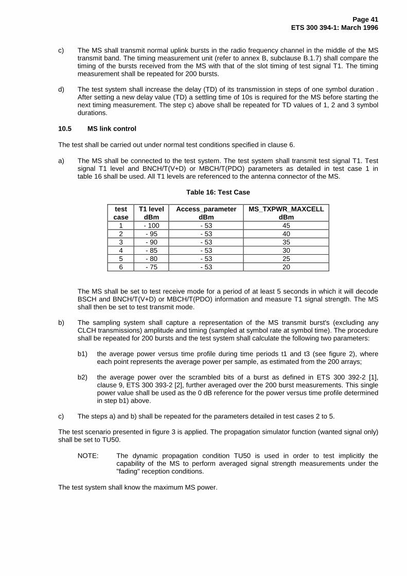
Page 41ETS 300 394-1: March 1996
c) The MS shall transmit normal uplink bursts in the radio frequency channel in the middle of the MStransmit band. The timing measurement unit (refer to annex B, subclause B.1.7) shall compare thetiming of the bursts received from the MS with that of the slot timing of test signal T1. The timingmeasurement shall be repeated for 200 bursts.
d) The test system shall increase the delay (TD) of its transmission in steps of one symbol duration .After setting a new delay value (TD) a settling time of 10s is required for the MS before starting thenext timing measurement. The step c) above shall be repeated for TD values of 1, 2 and 3 symboldurations.
10.5 MS link control
The test shall be carried out under normal test conditions specified in clause 6.
a) The MS shall be connected to the test system. The test system shall transmit test signal T1. Testsignal T1 level and BNCH/T(V+D) or MBCH/T(PDO) parameters as detailed in test case 1 intable 16 shall be used. All T1 levels are referenced to the antenna connector of the MS.
Table 16: Test Case
testcase
T1 leveldBm
Access_parameterdBm
MS_TXPWR_MAXCELLdBm
1 - 100 - 53 452 - 95 - 53 403 - 90 - 53 354 - 85 - 53 305 - 80 - 53 256 - 75 - 53 20
The MS shall be set to test receive mode for a period of at least 5 seconds in which it will decodeBSCH and BNCH/T(V+D) or MBCH/T(PDO) information and measure T1 signal strength. The MSshall then be set to test transmit mode.
b) The sampling system shall capture a representation of the MS transmit burst's (excluding anyCLCH transmissions) amplitude and timing (sampled at symbol rate at symbol time). The procedureshall be repeated for 200 bursts and the test system shall calculate the following two parameters:
b1) the average power versus time profile during time periods t1 and t3 (see figure 2), whereeach point represents the average power per sample, as estimated from the 200 arrays;
b2) the average power over the scrambled bits of a burst as defined in ETS 300 392-2 [1],clause 9, ETS 300 393-2 [2], further averaged over the 200 burst measurements. This singlepower value shall be used as the 0 dB reference for the power versus time profile determinedin step b1) above.
c) The steps a) and b) shall be repeated for the parameters detailed in test cases 2 to 5.
The test scenario presented in figure 3 is applied. The propagation simulator function (wanted signal only)shall be set to TU50.
NOTE: The dynamic propagation condition TU50 is used in order to test implicitly thecapability of the MS to perform averaged signal strength measurements under the"fading" reception conditions.
The test system shall know the maximum MS power.
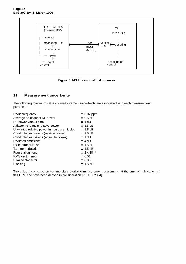
Page 42ETS 300 394-1: March 1996
TEST SYSTEM MS("serving BS")
setting
measuring PTx
comparison
PMS
coding ofcontrol
measuring
updating
decoding ofcontrol
settingPTx
TCH
BNCH(MCCH)
Figure 3: MS link control test scenario
11 Measurement uncertainty
The following maximum values of measurement uncertainty are associated with each measurementparameter.
Radio frequency ± 0.02 ppmAverage on channel RF power ± 0.5 dBRF power versus time ± 1 dBAdjacent channels relative power ± 1.5 dBUnwanted relative power in non transmit slot ± 1.5 dBConducted emissions (relative power) ± 1.5 dBConducted emissions (absolute power) ± 1 dBRadiated emissions ± 4 dBRx Intermodulation ± 1.5 dBTx Intermodulation ± 1.5 dBFrame alignment ± 2 x 10 -6
RMS vector error ± 0.01Peak vector error ± 0.03Blocking ± 1.5 dB
The values are based on commercially available measurement equipment, at the time of publication ofthis ETS, and have been derived in consideration of ETR 028 [4].
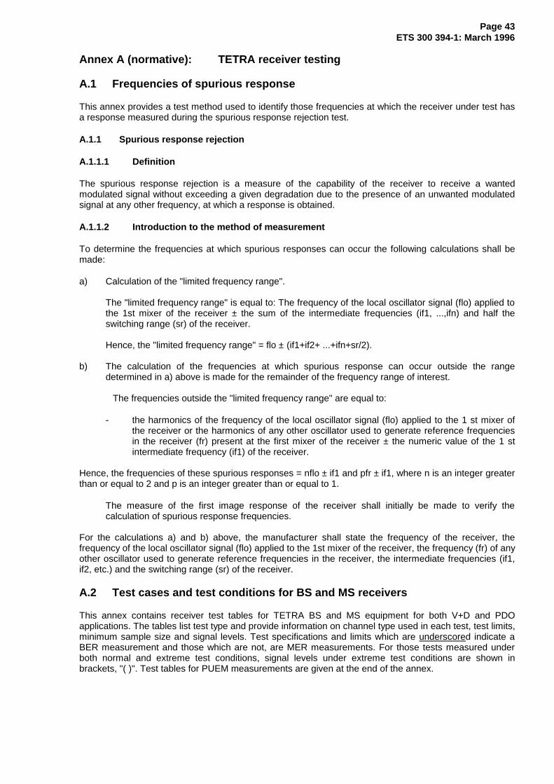
Page 43ETS 300 394-1: March 1996
Annex A (normative): TETRA receiver testing
A.1 Frequencies of spurious response
This annex provides a test method used to identify those frequencies at which the receiver under test hasa response measured during the spurious response rejection test.
A.1.1 Spurious response rejection
A.1.1.1 Definition
The spurious response rejection is a measure of the capability of the receiver to receive a wantedmodulated signal without exceeding a given degradation due to the presence of an unwanted modulatedsignal at any other frequency, at which a response is obtained.
A.1.1.2 Introduction to the method of measurement
To determine the frequencies at which spurious responses can occur the following calculations shall bemade:
a) Calculation of the "limited frequency range".
The "limited frequency range" is equal to: The frequency of the local oscillator signal (flo) applied tothe 1st mixer of the receiver ± the sum of the intermediate frequencies (if1, ...,ifn) and half theswitching range (sr) of the receiver.
Hence, the "limited frequency range" = flo ± (if1+if2+ ...+ifn+sr/2).
b) The calculation of the frequencies at which spurious response can occur outside the rangedetermined in a) above is made for the remainder of the frequency range of interest.
The frequencies outside the "limited frequency range" are equal to:
- the harmonics of the frequency of the local oscillator signal (flo) applied to the 1 st mixer ofthe receiver or the harmonics of any other oscillator used to generate reference frequenciesin the receiver (fr) present at the first mixer of the receiver ± the numeric value of the 1 stintermediate frequency (if1) of the receiver.
Hence, the frequencies of these spurious responses = nflo ± if1 and pfr ± if1, where n is an integer greaterthan or equal to 2 and p is an integer greater than or equal to 1.
The measure of the first image response of the receiver shall initially be made to verify thecalculation of spurious response frequencies.
For the calculations a) and b) above, the manufacturer shall state the frequency of the receiver, thefrequency of the local oscillator signal (flo) applied to the 1st mixer of the receiver, the frequency (fr) of anyother oscillator used to generate reference frequencies in the receiver, the intermediate frequencies (if1,if2, etc.) and the switching range (sr) of the receiver.
A.2 Test cases and test conditions for BS and MS receivers
This annex contains receiver test tables for TETRA BS and MS equipment for both V+D and PDOapplications. The tables list test type and provide information on channel type used in each test, test limits,minimum sample size and signal levels. Test specifications and limits which are underscored indicate aBER measurement and those which are not, are MER measurements. For those tests measured underboth normal and extreme test conditions, signal levels under extreme test conditions are shown inbrackets, "( )". Test tables for PUEM measurements are given at the end of the annex.

Page 44ETS 300 394-1: March 1996
Table A.1: Test conditions for MS receiver V+D, class A
Testtype
Channeltype
Logicalchannel
Propagationcondition
Signallevel (dBm)
Interfererlevel (dBm)
Spec.BER orMER %
Test limitBER orMER %
Minimumsample
sizenominal
error1 TCH/7,2 TU50 - 85 0,4 0,448 3,6E6
nominalerror
1 TCH/7,2 STAT - 20 0,1 0,122 170 000
sensitivity 2 SCH/F TU50 - 103 (- 97) 8 8,96 6 600sensitivity 2 AACH TU50 - 103 (- 97) 10 11,2 6 600sensitivity 3 BSCH HT200 - 103 11 12,32 4 800sensitivity 3 SCH/HD HT200 - 103 11 12,32 4 800sensitivity 4 AACH HT200 - 103 17 19,04 3 000sensitivity 4 TCH/2,4
N=1HT200 - 103 1,1 1,232 1,29E6
co-channelinterference
2 SCH/F HT200 - 85 - 104 7,5 8,4 7 000
adjacentchannel
interference
2 SCH/F TU50 - 100 (- 94) - 55 (- 59) 6,5 7,280 8 000
inter-modulation
1 TCH/7,2 STAT - 109 - 47 3,5 4,270 5 000
blocking 1 TCH/7,2 STAT - 109 - 25 3,5 4,270 5 000spuriousresponse
1 TCH/7,2 STAT - 109 - 45 3,5 4,270 5 000
Table A.2: Test conditions for MS receiver V+D, class B
Testtype
Channeltype
Logicalchannel
Propagationcondition
Signallevel (dBm)
Interfererlevel (dBm)
Spec.BER orMER %
Test limitBER orMER %
Minimumsample
sizenominal
error1 TCH/7,2 TU50 - 85 0,4 0,448 3,6E6
nominalerror
1 TCH/7,2 STAT - 20 0,1 0,122 170 000
sensitivity 2 SCH/F TU50 - 103 (- 97) 8 8,96 6 600sensitivity 2 AACH TU50 - 103 (- 97) 11 12,32 6 600sensitivity 3 BSCH TU50 - 103 8 8,96 6 600sensitivity 3 SCH/HD TU50 - 103 9 10,08 6 600sensitivity 4 AACH TU50 - 103 10 11,2 5 000sensitivity 4 TCH/2,4
N=1TU50 - 103 0,35 0,392 2,16E6
co-channelinterference
2 SCH/F TU50 - 85 - 104 6,5 7,280 8 500
adjacentchannel
interference
2 SCH/F TU50 - 100 (- 94) - 55 (- 59) 6,5 7,280 8 000
inter-modulation
1 TCH/7,2 STAT - 109 - 47 4 4,880 4 500
blocking 1 TCH/7,2 STAT - 109 - 25 4 4,880 4 500spuriousresponse
1 TCH/7,2 STAT - 109 - 45 4 4,880 4 500

Page 45ETS 300 394-1: March 1996
Table A.3: Test conditions for MS receiver V+D, class E
Test type Channeltype
Logicalchannel
Propagationcondition
Signallevel (dBm)
Interfererlevel (dBm)
Spec.BER orMER %
Test limitBER orMER %
Minimumsample
sizenominal
error1 TCH/7,2 TU50 - 85 0,4 0,448 3,6E6
nominalerror
1 TCH/7,2 STAT - 20 0,1 0,122 170 000
sensitivity 2 SCH/F TU50 - 103 (- 97) 8 8,96 6 600sensitivity 2 AACH TU50 - 103 (- 97) 10 11,2 6 600sensitivity 3 BSCH EQ200 - 103 22 24,64 2 000sensitivity 3 SCH/HD EQ200 - 103 21 23,52 2 000sensitivity 4 AACH EQ200 - 103 16 17,92 3 000sensitivity 4 TCH/2,4
N=1EQ200 - 103 0,82 0,918 1,29E6
co-channelinterference
2 SCH/F EQ200 - 85 - 104 20 22,400 3 500
adjacentchannel
interference
2 SCH/F TU50 - 100 (- 94) - 55 (- 59) 6,5 7,280 8 000
inter-modulation
1 TCH/7,2 STAT - 109 - 47 3,5 4,270 4 500
blocking 1 TCH/7,2 STAT - 109 - 25 3,5 4,270 4 500
Table A.4: Test conditions for MS receiver PDO, class A
Test type
Channeltype
Logicalchannel
Propagationcondition
Signallevel (dBm)
Interfererlevel (dBm)
Spec.MER %
Test limitMER %
Minimumsample
sizesensitivity 6 NBCH HT200 - 103 11 12,32 4 500sensitivity 5 MBCH HT200 - 103 11 12,32 4 500sensitivity 6 NBCH TU50 - 103 (- 97) 8 8,96 6 500sensitivity 5 MBCH TU50 - 103 (- 97) 8 8,96 6 500
co-channelinterference
6 NBCH TU50 - 85 - 104 7 7,84 9 000
co-channelinterference
5 MBCH TU50 - 85 - 104 6 6,720 9 000
adjacentchannel
interference
6 NBCH TU50 - 100 (- 94) - 55 (- 59) 7 7,84 9 000
inter-modulation
6 NBCH STAT - 109 - 47 2,5 3,050 6 500
blocking 6 NBCH STAT - 109 - 25 2,5 3,050 6 500spuriousresponse
6 NBCH STAT - 109 - 45 2,5 3,050 6 500

Page 46ETS 300 394-1: March 1996
Table A.5: Test conditions for MS receiver PDO, class B
Testtype
Channeltype
Logicalchannel
Propagationcondition
Signallevel (dBm)
Interfererlevel (dBm)
Spec.MER %
Test limitMER %
Minimumsample
sizesensitivity 6 NBCH TU50 - 103 (- 97) 8 8,96 6 500sensitivity 5 MBCH TU50 - 103 8 8,96 6 500
co-channelinterference
6 NBCH TU50 - 85 - 104 7 7,840 9 000
co-channelinterference
5 MBCH TU50 - 85 - 104 6 6,720 9 000
adjacentchannel
interference
6 NBCH TU50 - 100 (- 94) - 55 (- 59) 7 7,840 9 000
inter-modulation
6 NBCH STAT - 109 - 47 2,5 3,050 6 500
blocking 6 NBCH STAT - 109 - 25 2,5 3,050 6 500spuriousresponse
6 NBCH STAT - 109 - 45 2,5 3,050 6 500
Table A.6: Test conditions for MS receiver PDO, class E
Testtype
Channeltype
Logicalchannel
Propagationcondition
Signal level (dBm)
Interfererlevel (dBm)
Spec.MER %
Test limitMER %
Minimumsample
sizesensitivity 6 NBCH EQ200 - 103 22 24,64 2 000sensitivity 5 MBCH EQ200 - 103 21 23,52 2 000sensitivity 6 NBCH TU50 - 103 (- 97) 8 8,96 6 500sensitivity 5 MBCH TU50 - 103 8 8,96 6 500
co-channelinterference
6 NBCH TU50 - 85 - 104 7 7,840 2 500
co-channelinterference
5 MBCH TU50 - 85 - 104 6 6,720 2 500
adjacent-channel
interference
6 NBCH TU50 - 100 (- 94) - 55 (- 59) 7 7,840 9 000
inter-modulation
6 NBCH STAT - 109 - 47 2,5 3,050 6 500
blocking 6 NBCH STAT - 109 - 25 2,5 3,050 6 500spuriousresponse
6 NBCH STAT - 109 - 45 2,5 3,050 6 500

Page 47ETS 300 394-1: March 1996
Table A.7: Test conditions for BS receiver V+D, class A
Testtype
Channeltype
Logicalchannel
Propagationcondition
Signal level (dBm)
Interfererlevel (dBm)
Spec.BER orMER %
Test limitBER or MER
%
Minimumsample
sizenominal
error7 TCH/7,2 TU50 - 85 0,4 0,448 3,6E6
nominalerror
7 TCH/7,2 STAT - 20 0,1 0,122 170 000
sensitivity 8 SCH/F TU50 - 106 (- 100) 11 12,32 6 600sensitivity 9 STCH TU50 - 106 (- 100) 9 10,08 6 600sensitivity 10 TCH/2,4
N=1HT200 - 106 (- 100) 1,3 1,456 45 000
sensitivity 11 SCH/HU HT200 - 106 (- 100) 9,5 10,64 5 000co-channelinterference
8 SCH/F HT200 - 85 - 104 7,5 8,4 7 000
adjacentchannel
interference
8 SCH/F TU50 - 103 (- 97) - 58 (- 62) 6 6,72 9 000
inter-modulation
7 TCH/7,2 STAT - 112 - 47 3.0 3,66 5 800
blocking 7 TCH/7,2 STAT - 112 - 25 3.0 3,66 5 800spuriousresponse
7 TCH/7,2 STAT - 112 - 45 3.0 3,66 5 800
Table A.8: Test conditions for BS receiver V+D, class B
Testtype
Channeltype
Logicalchannel
Propagationcondition
Signal level (dBm)
Interfererlevel (dBm)
Spec. BERor MER %
Test limitBER orMER %
Minimumsample
sizenominal
error7 TCH/7,2 TU50 - 85 0,4 0,448 3.6E6
nominalerror
7 TCH/7,2 STAT - 20 0,1 0,122 170 000
sensitivity 8 SCH/F TU50 - 106 (- 100) 8 8,96 6 600sensitivity 9 STCH TU50 - 106 (- 100) 8 8,96 6 600sensitivity 10 TCH/2,4
N=1TU50 - 106 (- 100) 0,35 0,392 160 000
sensitivity 11 SCH/HU TU50 - 106 (- 100) 8 8,96 6 600co-channelinterference
8 SCH/F TU50 - 85 - 104 7,5 8,4 7 000
adjacentchannel
interference
8 SCH/F TU50 - 103 (- 97) - 58 (- 62) 6 6,72 9 000
inter-modulation
7 TCH/7,2 STAT - 112 - 47 4,0 4,88 4 000
blocking 7 TCH/7,2 STAT - 112 - 25 4,0 4,88 4 000spuriousresponse
7 TCH/7,2 STAT - 112 - 45 4,0 4,88 4 000

Page 48ETS 300 394-1: March 1996
Table A.9: Test conditions for BS receiver PDO, class A
Testtype
Channeltype
Logicalchannel
Propagationcondition
Signal level(dBm)
Interfererlevel (dBm)
Spec.MER %
Test limitMER %
Minimumsample
sizesensitivity 12 NBCH HT200 - 106 11 12,32 4 500sensitivity 12 NBCH TU50 - 106 9 10,08 6 600
co-channelinterference
.
12 NBCH TU50 - 85 - 104 7 7,84 9 000
adjacentchannel
interference
12 NBCH TU50 - 103 (- 97) - 58 (- 62) 7 7,84 9 000
inter-modulation
12 NBCH STAT - 112 - 47 9 10,08 6 600
blocking 12 NBCH STAT - 112 - 25 9 10,08 6 600spuriousresponse
12 NBCH STAT - 112 - 45 9 10,08 6 600
Table A.10: Test conditions for BS receiver PDO, class B
Testtype
Channeltype
Logicalchannel
Propagationcondition
Signal level (dBm)
Interfererlevel (dBm)
Spec.MER %
Test limitMER %
Minimumsample
sizesensitivity 12 NBCH TU50 - 106 (- 100) 8 8,96 6 600
co-channelinterference
12 NBCH TU50 - 85 - 104 7 7,84 9 000
adjacentchannel
interference
12 NBCH TU50 - 103 (- 97) - 58 (- 62) 7 7,84 9 000
inter-modulation
12 NBCH STAT - 112 - 47 5 5,6 10 000
blocking 12 NBCH STAT - 112 - 25 5 5,6 10 000spuriousresponse
12 NBCH STAT - 112 - 45 5 5,6 10 000
Table A.11: PUEM Test table
Equipmenttype
Channeltype
Logicalchannel
Propagationcondition
Signal level (dBm)
Spec.PUEM
Test limitPUEM
Max No.Errors
Samplesize
MS(V+D) 2 SCH/FAACH
TU50 - 103 10-5
10-43,5 x 10⁻⁴ 6,5
x 10-428
31 200
MS(PDO) 6 NBCH TU50 - 103 10-5 3,5 x 10⁻⁴ 2 31 200BS(V+D) 8 SCH/F TU50 - 106 10-5 3,5 x 10⁻⁴ 2 31 200BS(PDO) 12 NBCH TU50 - 106 10-5 3,5 x 10⁻⁴ 2 31 200

Page 49ETS 300 394-1: March 1996
A.3 Test signal T1, content of BSCH and BNCH/T (V+D) & MBCH/T (PDO)
The following tables define the information content of the BSCH and BNCH/T for V+D and MBCH/T forPDO bursts, used during testing.
Table A.12: Test signal T1 content of the BSCH (V+D) & MBCH/T (PDO)
Information element Size(bits)
Values Meaning
System code 4 0xxx1xxx
V+D reservedPDO reserved
Colour code 6 111111 ScrambledTimeslot number 2 00 Timeslot 1Frame number 5 01010 Frame 18
Multiframe number 6 111100 Multiframe 60Sharing mode 2 00 Continuous transmission
TS reserved frames 3 xxx do not careU-plane DTX 1 x do not care
Frame 18 extension 1 x do not careReserved 1 x do not care
TM-SDU (MLE data) 29 mobile country code, mobile network code, cellservice level information set by test system (defined
in ETS 300 392-2 [1], clause 18)

Page 50ETS 300 394-1: March 1996
Table A.13: Test signal T1 content of the BNCH/T(V+D) & MBCH/T (PDO)
Information element Size(bits)
Values Meaning
PDU type 2 10 Broadcast PDUBroadcast type 2 00 SYSINFO PDU
Main carrier 12 test signal carrier frequencyFrequency band 4 test signal carrier band
Offset 2 xx do not careDuplex spacing 3
Reverse operation 1 01
normal (defined in ETS 300 392-2 [1], clause 21)reverse
No of common secondarycontrol channels in use
2 00 none
MS_TXPWR_MAX_CELL 3 000001010011100101110111
reserved15 dBm20 dBm25 dBm30 dBm35 dBm40 dBm45 dBm
RXLEV_ACCESS_MIN 4 000000 Defined in ETS 300 392-2 [1], clause 21ACCESS_PARAMETER 4 0000 - 1111 - 53 dBm to - 23 dBm in 2 dB steps for
subsequent power adjustmentsRADIO_DOWNLINK_
TIMEOUT4 0000 Disable Radio Downlink Counter (RDC)
Tx_on 1 01
Reception onTransmission on
Tx_burst_type 1 01
Normal uplink burstControl uplink burst
T1_burst_type 4 0000000001000100001100100001010011000111010000100101010010110110001101011100111110000
10001-11111
type 0: TCH/7,2 (downlink)type 1: TCH/7,2 (downlink)type 2: SCH/F(downlink)
type 3: BSCH +SCH/HD (downlink)type4: TCH/2,4 N=1 (downlink)type 5: MBCH (PDO downlink)type 6: NBCH (PDO downlink)
type 7: TCH/7,2 (uplink)type 8: SCH/F (uplink)
type 9: STCH + STCH (uplink)type 10: TCH/2,4 N=1 (uplink)
type 11: SCH/HU + SCH/HU (uplink)type 12: NBCH (PDO uplink)
type 13: random synchronization burststype 14: random synchronization sub-bursts
type 15: TCH/S (downlink)type 16: TCH/S (uplink)
reservedreserved 72 do not care

Page 51ETS 300 394-1: March 1996
Annex B (normative): Radio test system functions
B.1 Test transmitter and receiver
B.1.1 General
The task of the test transmitter/receiver is to simulate either TETRA base station or mobile stationfunctions required while performing the Radio Conformance Testing procedures on the TETRA equipmentaccording to the clauses 8, 9 and 10. These tasks include:
- supporting all the logical channels defined in TETRA;
- supporting the full range of transmit and receive frequencies of TETRA according toETS 300 392-2 [1], clause 6;
- transmitting at power levels from - 115 dBm to - 20 dBm, adjustable in steps of 0,2 dB or less, witha maximum level uncertainty of ± 1 dB and with a maximum frequency uncertainty of ± 0,02 ppm;
- delaying the transmitted bursts in steps of less than or equal to 1/4 symbol duration, wheneverrequired;
- receiving power levels with a dynamic range of at least 40 dB;
- activating and de-activating specific test modes in the MS, whenever required (optional feature).
B.1.2 Sampling system
B.1.2.1 General
The task of the sampling system, a subsystem of the test receiver, is to acquire a sampled version of awanted TETRA modulated radio signal or an unwanted emission through the TETRA filter. The acquiredcomplex samples (I-Q base band representation) are used for modulation accuracy and powermeasurements.
A sampling rate of at least 4 samples per symbol duration is sufficient. The receive frequency of thesampling system shall be adjustable to the nominal equipment transmit frequencies with an uncertainty of± 0,02 ppm. Prior to sampling frequency down conversion from RF to IF and appropriate IF filtering maytake place.
In order to provide credible test results the sampling system, when connected to the test transmitter, shallmeet the requirements defined in the subclauses B.1.2.2 to B.1.2.4. It is assumed that the test signals T1and T2 themselves meet the requirements given in subclauses B.1.2.2 to B.1.2.4.
B.1.2.2 TETRA filter
The TETRA filter is the receive filter of the sampling system. Its characteristics are implicitly defined, asfar as necessary, by the requirements for the sampling system defined in subclauses B.1.2.3 to B.1.2.5.
B.1.2.3 Adjacent channel power measurements
The residual adjacent channel level of the test system, as measured in subclause 8.3, shall not exceedthe limits shown in table B.1.1, at the listed frequency offsets from the nominal carrier frequencies, whentest signal T2 is applied.
Table B.1: Maximum residual adjacent channel level of the test system
Frequency offset Maximum level25 kHz - 70 dBc50 kHz - 80 dBc75 kHz - 80 dBc

Page 52ETS 300 394-1: March 1996
B.1.2.4 Modulation accuracy measurements
The residual modulation accuracy of the test system shall meet the limit specified in subclause 7.3.1.1,when transmitting either a continuous or discontinuous test signal T1. The residual RMS vector error shallbe less than 0,03 and the peak vector error shall be less than 0,1.
B.1.2.5 Measurement of unwanted output power in the non-active transmit state
In the non-active transmit state the output level measured as defined in subclass 7.1.2 shall not exceedthe following limits:
- Lmin = - 60 dBc when a discontinuous test signal T1 consisting of one uplink burst per frame isapplied;
- Lmin = - 35 dBc when a discontinuous test signal T1 consisting of one discontinuous downlink burstper frame is applied.
No extra ramping function is applied to the test signals T1 which leads to slightly increased levelscompared to those specified for Lmin in ETS 300 392-2 [1], clause 6. Nevertheless this requirementimposes an additional constraint to the TETRA filter and shall contribute to ensure its correctimplementation
B.1.3 Spectrum analyzer
A spectrum analyzer is to be used as a power detecting device (in frequency domain) and is characterisedas follows:
- frequency range: 9 kHz to 4 GHz;
- power level range: - 80 dBm to + 20 dBm;
- measurement uncertainty of power level: ± 1,5 dB (100 kHz to 1 GHz), ± 3,0 dB (1 GHz to 4 GHz);
- dynamic range: 80 dB;
- resolution bandwidths: 30 kHz, 100 kHz, 300 kHz, 1 MHz, 3 MHz;
- video bandwidths: 30 kHz, 100 kHz, 300 kHz, 1 MHz, 3 MHz;
- peak hold function selectable.
B.1.4 Error rate tester
The task of the error rate tester is to generate test bit sequences which are to be sent to the receiverunder test. A Pseudo Random Bit Sequence (PRBS) with a length of 511 bits shall be used according toCCITT Recommendation O.153 [3]. The second task is to compare the bits decoded by the receiver undertest with the original ones and calculate the appropriate error rates.
B.1.5 Interfering signal sources
a) First interferer:
- modulation: TETRA modulated (see test signal T2 in subclause 5.3.3);
- frequency range: nominal TETRA MS receive frequencies;
- uncertainty of frequency: ± 0,2 ppm;
- power level range; - 110 dBm to - 30 dBm, adjustable in steps of 1 dB or less;
- uncertainty of power level: ± 1,0 dB.

Page 53ETS 300 394-1: March 1996
b) Second interferer:
- modulation: un-modulated sinusoidal signal (see test signal T3 in subclause 5.3.4);
- frequency range: 10 MHz to 4 GHz;
- uncertainty of frequency: ± 0,2 ppm;
- power level range: - 60 dBm to 0 dBm, level adjustable in steps of 1 dB or less;
NOTE: Up to + 20 dBm in the MS transmit band; for intermodulation attenuation measurementonly.
- uncertainty of power level; ± 1,0 dB.
B.1.6 Propagation simulators
The task of the propagation simulators is to take into account the effect of the propagation conditions, asdescribed in ETS 300 392-2 [1], clause 6, while testing the receiver performance.
B.1.7 Timing measurement unit
The timing measurement unit is a time interval counter within the test system. It compares the timing(training sequence) of bursts received by the test receiver with the internal timing reference of the testsystem. The bursts (training sequences) transmitted by the test transmitter shall be synchronised to thisinternal timing reference.
B.1.8 Passive test system components
The task of the passive components is to establish the appropriate interconnection of the test system andthe equipment under test. The required composition and characteristics of the passive componentsdepend on the overall implementation of the test system and are not to be defined in this specification.However, the following components may be useful herein: RF combiner, power splitter, isolating device,RF attenuators and connecting cables.
B.1.9 Test system controller
The test system controller co-ordinates the test system functions via an appropriate interface. It may alsoperform the calculations required by the test procedures and present the final test results wheneverappropriate.
B.1.10 Test signal (T1, T2) requirements
B.1.10.1 Adjacent channel power
Adjacent channel power, measured in a TETRA filter, shall not exceed the limits shown in table B.1.2, atthe listed frequency offsets from the nominal carrier frequencies.
Table B.2: Maximum adjacent channel power levels of the test transmitter
Frequency offset Max. level25 kHz - 70 dBc50 kHz - 80 dBc75 kHz - 80 dBc
NOTE: The TETRA filter to be used for this purpose can be approximately realised byweighted integration over frequency of the adjacent channel spectrum measured with aspectrum analyzer using a narrow filter. The weighting function is the squaredmagnitude frequency response of the ideal TETRA filter.

Page 54ETS 300 394-1: March 1996
B.1.10.2 Modulation accuracy
The RMS vector error and the peak vector error in any burst as defined in ETS 300 392-2 [1], clause 6shall be less than 0,03 and 0,1, respectively. These errors shall be measured by observing the test signalsT1 and T2 through a TETRA filter having the same sampled impulse response g'j.
NOTE: Verification of modulation accuracy can be performed by the test transmitter itselfusing a built-in Cartesian loop-back facility.
Maximum acceptable measurement uncertainty:
± 0,01 for RMS and ± 0,03 for peak vector error measurement.

Page 55ETS 300 394-1: March 1996
History
Document history
January 1995 Public Enquiry PE 78: 1995-01-30 to 1995-05-26
November 1995 Vote V 91: 1995-11-06 to 1995-12-29
March 1996 First Edition
ISBN 2-7437-0563-9Dépôt légal : Mars 1996

![EUROPEAN ETS 300 742 TELECOMMUNICATION …This ETS mainly is based on ETS 300 300 [13], being responsible for the bit rates 155 520 kbit/s and 622 080 kbit/s and the ITU-T Recommendation](https://img.pdfslide.us/doc/110x75/5f4931b4fc46f1542e025226/european-ets-300-742-telecommunication-this-ets-mainly-is-based-on-ets-300-300-13.jpg)


![EUROPEAN ETS 300 799 TELECOMMUNICATION STANDARD€¦ · ETS 300 799: September 1997 Introduction This ETS is one of a set associated with ETS 300 401 [1] describes the transmitted](https://img.pdfslide.us/doc/110x75/602b481e7085d253135ff9e5/european-ets-300-799-telecommunication-standard-ets-300-799-september-1997-introduction.jpg)