Embed Size (px)
Citation preview

Ethernet System Hardware on AM-Class Devices
Technical Overview: Hardware
1

Agenda • OSI Model Description
– Physical Layer
• Ethernet Interfaces Overview – MII – RMII – RGMII
• Ethernet PHY/MAC Management – MDIO
• Ethernet Interface Layout Considerations – Length Matching – Reference Planes – Via Spacing
2

OSI Model Description
Ethernet System HW/SW on AM-Class Devices
3

OSI: Open Systems Interconnect Model
4
Host Layers
Media Layers
1
2
3
4
5
6
7 • Partitions a communication system into seven functional abstraction layers.
• Characterizes and standardizes the communication functions of a telecommunication or computing system without regard to their underlying internal structure and technology.
• Ensures the interoperability of diverse communication systems with standard protocols.

OSI: Open Systems Interconnect Model
5
Host Layers
Media Layers
1
2
3
4
5
6
7 Each of the seven OSI layers exchanges information with its immediate neighbor (peer) via the Protocol Data Unit (PDU) structure. Data to be transmitted is composed at the top-most layer of the transmitting device and passed as a PDU to Layer n-1.
As each layer processes the PDU, it is passed downward until reaching Layer 1, where the bits are transmitted to the receiving device. BITS
TRA
NS
MIT
DATA

OSI: Open Systems Interconnect Model
6
Host Layers
Media Layers
1
2
3
4
5
6
7 At the receiving device, the flow is reversed. The data is passed from the lowest to the highest layer for consumption by the host.
RE
CE
IVE
BITS
DATA

OSI: Open Systems Interconnect Model
7
Host Layers
Media Layers
1
2
3
4
5
6
7

Ethernet Interfaces Overview
Ethernet System HW/SW on AM-Class Devices
8

9
AM-Class Devices: Ethernet Interface Overview

10
AM-Class Devices: Ethernet Interface Overview

AM-Class Devices: Ethernet Interface Overview
11
Ethernet MAC (Media Access Control)
Ethernet PHY (PHYsical Layer)
Ethernet Port (RJ-45)

Common Platform Switch (CPSW)
12
RMII/RGMII/MII_1
MDIO
RMII/RGMII/MII_2
PORT 1
PORT 2 PORT 0
13
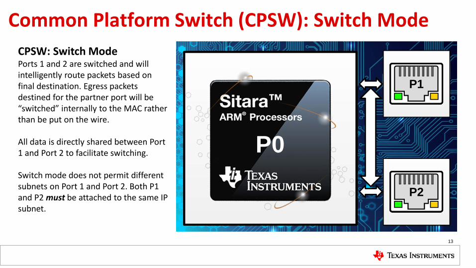
P0
P1
P2
CPSW: Switch Mode Ports 1 and 2 are switched and will intelligently route packets based on final destination. Egress packets destined for the partner port will be “switched” internally to the MAC rather than be put on the wire. All data is directly shared between Port 1 and Port 2 to facilitate switching. Switch mode does not permit different subnets on Port 1 and Port 2. Both P1 and P2 must be attached to the same IP subnet.
Common Platform Switch (CPSW): Switch Mode

14
P0
P1
P2
CPSW: Dual-MAC Mode Ports 1 and 2 are independent. All packets to and from the external ports are routed to Port 0 regardless of source or destination. No data is shared between Port 1 and Port 2. This applies to both ingress and egress packets. This mode provides “two LAN card” functionality and as such Port 1 and Port 2 can be attached to different IP subnets.
Common Platform Switch (CPSW): Dual-MAC Mode

AM-Class Devices: PHY/MAC Ethernet Interfaces
15

PHY/MAC Ethernet Interfaces: MII
16
MII (Media Independent Interface) • 16-pin interface • Supports interface speeds of 10/100Mbps • Discrete TX and RX clocking (2.5/25MHz)

PHY/MAC Ethernet Interfaces: RMII
17
RMII (Reduced Media Independent Interface) • 8-pin interface • Supports interface speeds of 10/100Mbps • Shared clock for both TX and RX (50MHz)
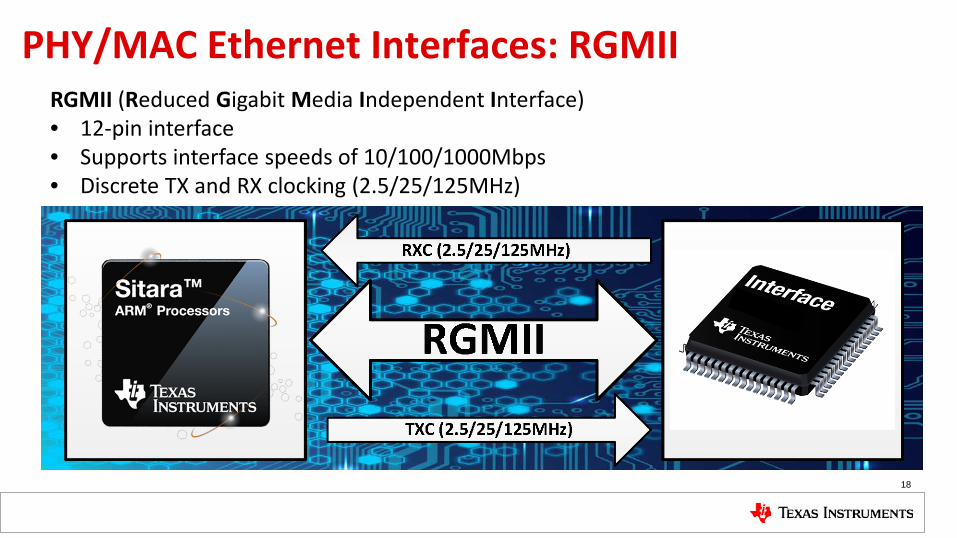
PHY/MAC Ethernet Interfaces: RGMII
18
RGMII (Reduced Gigabit Media Independent Interface) • 12-pin interface • Supports interface speeds of 10/100/1000Mbps • Discrete TX and RX clocking (2.5/25/125MHz)

Ethernet PHY/MAC Management
Ethernet System HW/SW on AM-Class Devices
19

AM-Class Devices: PHY/MAC Management
20

MDIO (Management Data Input/Output)
21
MDIO (Management Data Input/Output) provides a bidirectional management interface for the PHYs and MACs to communicate with each other. Many of the functions of the PHY are performed autonomously. So MDIO is needed to exchange information in parallel to the PHY/MAC data interface. MDIO Detail: • 2-pin interface:
• Data (MDIO) • Clock (MDC)
• 2.5MHz Clock • Shared bus for up to 32 PHY devices • Continuously polled*
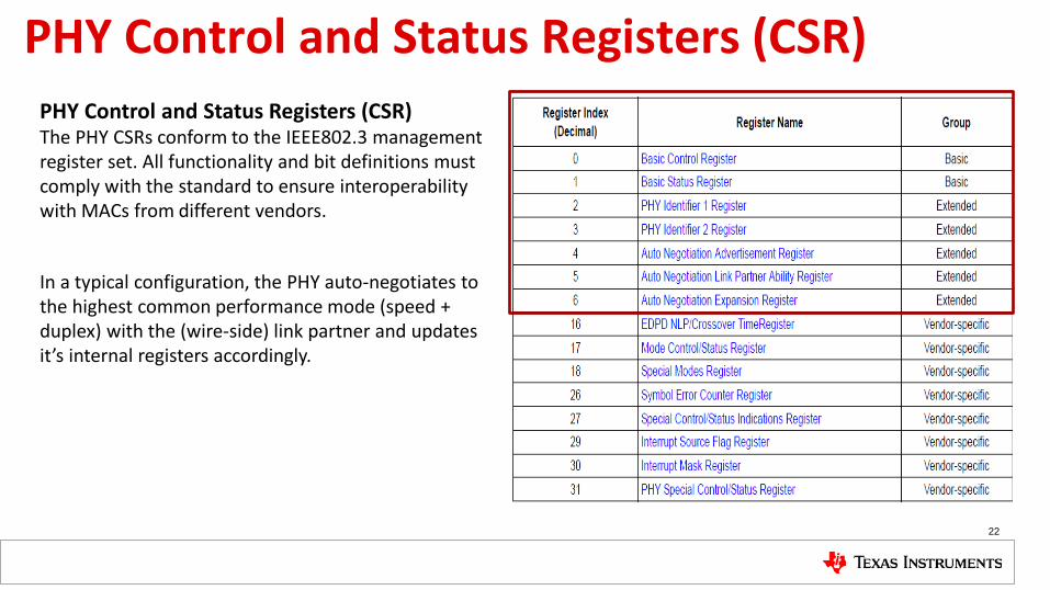
PHY Control and Status Registers (CSR)
22
PHY Control and Status Registers (CSR) The PHY CSRs conform to the IEEE802.3 management register set. All functionality and bit definitions must comply with the standard to ensure interoperability with MACs from different vendors.
In a typical configuration, the PHY auto-negotiates to the highest common performance mode (speed + duplex) with the (wire-side) link partner and updates it’s internal registers accordingly.

PHY/MAC Management via MDIO
23
MDIO

Debugging PHY: Basic Control Register
24
Basic Control Register (PHY Index 0)
• Is the PHY in Isolate Mode?
• Is the PHY powered-up?
• Is the PHY in Loopback Mode?

Debugging PHY: Basic Status Register
25
Basic Status Register (PHY Index 1)
• Ensure that the Link is up.
• Check for remote faults.
• Was Auto-Negotiation successful?

Debugging PHY: Auto Negotiation Advertisement
26
Auto-Negotiation Advertisement (PHY Index 4)
• Is the PHY configured/strapped correctly?
• Check for remote faults.

Debugging PHY: Auto Negotiation Link Partner
27
Auto-Negotiation Link Partner Ability (PHY Index 5)
• Is the Link Partner configured correctly?
• Check for remote faults.

Debugging PHY: MAC Control Register
28
MAC Control Register (MAC CPSW_SL Address 0x04)
• Is the link speed correct?
• Is GIG mode set?
• Is the interface enabled?

Debugging PHY: CPSW_STATS
29
CPSW_STATS (MAC CPSW_STATS 0x00-0x8C)
• Does the Good TX+ Good RX frame count increment?
• Are RX CRC Errors present?

Ethernet Interfaces: PCB Layout Considerations
Ethernet System HW/SW on AM-Class Devices
30

PCB Layout Best Practices
31
A primary concern when designing a system that implements one or more high-speed interfaces is accommodating and isolating the relevant high-speed signals. High-speed signals are most likely to impact, or be impacted by, other signals on the board. As a result, they must be laid out early (preferably first) in the PCB design process to ensure that prescribed routing rules can be followed. High-speed PCB layout best practices include: • Do not place probe or test points on any high-speed signal. • Do not route high-speed traces under or near crystals, oscillators, clock signal generators,
switching power regulators, mounting holes, magnetic devices, or ICs that use or duplicate clock signals.
• Ensure that high-speed signals are routed ≥ 90 mils from the edge of the reference plane. • Maximize keep-out spacing when possible. • After BGA breakout, keep high-speed signals clear of the SoC as high-current transients
produced during internal state transitions can be difficult to filter out.

PCB Layout: Length Matching
32
Length Matching: Match the etch lengths of the relevant traces of each interface. When matching the length of the high-speed signals (clock/data), add serpentine routing to match the lengths as close to the mismatched ends as possible.

PCB Layout: Reference Planes
33
Reference Planes: High-speed signals should be routed over a solid GND reference plane and not across a plane split or a void in the reference plane unless absolutely necessary. TI does not recommend high-speed signal references to power planes. Routing across a plane split or a void in the reference plane forces return high-frequency current to flow around the split or void. This can result in the following conditions: • Excess radiated emissions from an unbalanced current flow • Delays in signal propagation delays due to increased series inductance • Interference with adjacent signals • Degraded signal integrity (that is, more jitter and/or reduced signal amplitude)

PCB Layout: Reference Planes Example
34
PLANE VOID
n>=(Tracewidth * 1.5)
n
nn
PLANE VOID

PCB Layout: Stitching Capacitors
35
If routing over a plane-split is completely unavoidable, place stitching capacitors across the split to provide a return path for the high-frequency current. These stitching capacitors minimize the current loop area and any impedance discontinuity created by crossing the split. These capacitors should be 1μF or lower and placed as close as possible to the plane crossing.
Signal Plane Signal Plane Signal Plane Signal Plane

PCB Layout: Via Equalization and Spacing
36
Equalize Via Count: If using vias is necessary on a high-speed Ethernet signal trace, ensure that the via count on each member of the data bus is equal and that the vias are as evenly spaced as possible. TI recommends placing vias as close as possible to the SoC. Signal Isolation: To minimize crosstalk in Ethernet interface implementations, the spacing between the signals should be a minimum of 3 times the width of the trace. This spacing is referred to as the 3W rule. A PCB design with a trace width of 6 mils requires a minimum of 18 mils spacing between high-speed signals. Where the high-speed Ethernet signals abut a clock or a other periodic signal, increase this keep-out to a minimum of 50 mils to ensure proper isolation.

For More Information • High Speed Interface Layout Guidelines: http://www.ti.com/cn/lit/pdf/spraar7
• TI Ethernet PHYs: http://www.ti.com/lsds/ti/interface/ethernet-overview.page
• IEEE 802.3: Ethernet: http://standards.ieee.org/about/get/802/802.3.html
• For questions regarding topics covered in this training, visit the support forums at the TI E2E Community website: http://e2e.ti.com