Embed Size (px)
Citation preview

Etching - Chapter 10
SILICON VLSI TECHNOLOGYFundamentals, Practice and ModelingBy Plummer, Deal & Griffin
© 2000 by Prentice HallUpper Saddle River NJ
1
ETCHING – Chapter 10
Substrate
Film deposition Photoresist application
Deposited Film Photoresist
Exposure
Development Etching Resist removal
Mask
Etch mask
Light
• Etching of thin films and sometimes the silicon substrate are very common process steps.• Usually selectivity, and directionality are the first order issues.• Selectivity comes from chemistry; directionality usually comes from physical processes. Modern etching techniques try to optimize both.• Simulation tools are beginning to play an important role in etching just as they are in deposition. Topography simulators often do both, based on the same physical principles.

Etching - Chapter 10
SILICON VLSI TECHNOLOGYFundamentals, Practice and ModelingBy Plummer, Deal & Griffin
© 2000 by Prentice HallUpper Saddle River NJ
2
a)
b)
a) isotropic b) anisotropic c) completely anisotropic
More directional etching
• Illustration of undercutting (directionality) and selectivity issues.
• Usually highly anisotropic (almost vertical profiles) and highly selective etching (ratios of 25-50) are desired, but these can be difficult to achieve simultaneously.
General etch requirements:1. Obtain desired profile (sloped or vertical)2. Minimal undercutting or bias3. Selectivity to other exposed films and resist4. Uniform and reproducible5. Minimal damage to surface and circuit6. Clean, economical, and safe

Etching - Chapter 10
SILICON VLSI TECHNOLOGYFundamentals, Practice and ModelingBy Plummer, Deal & Griffin
© 2000 by Prentice HallUpper Saddle River NJ
3
Historical Development and Basic Concepts• There are two main types of etching used in IC fabrication: wet etching and dry or plasma etching. Plasma etching dominates today.
Wet Etching and General Etching Ideas
• Processes tend to be highly selective but isotropic (except for crystallographically dependent etches).Examples:Etching of SiO2 by aqueous HF: (1)
Etching of Si by nitric acid (2)(HNO3) and HF:
�
SiO2 + 6HF→ H2SiF6 + 2H2O
�
Si + HNO3 + 6HF → H2SiF6 + HNO2 + H2O + H2
• Wafers typically submerged in specific chemical baths and rinsed in DI H2O.

Etching - Chapter 10
SILICON VLSI TECHNOLOGYFundamentals, Practice and ModelingBy Plummer, Deal & Griffin
© 2000 by Prentice HallUpper Saddle River NJ
4
b
d
b
d = xf
a) b)
• Isotropic etching implies undercutting. This is often expressed in terms of the etch bias b.• Etch anisotropy is defined as: (3)
• Af = 0 for isotropic etching since rlat = rver. • Some overetching, shown above at right, is usually done to ensure complete etching (due to variations in film thickness and etch rate). • Selectivity is usually excellent in wet etching ( ) since chemical reactions are very selective.
Δm Δma) b)
�
Af = 1− rlatrver
= 1− bd
�
S = r1 / r2
• Mask erosion can be an issue for both isotropic and anisotropic etching profiles.• Because of their isotropic nature, wet chemical etches are rarely used in mainstream IC manufacturing today.

Etching - Chapter 10
SILICON VLSI TECHNOLOGYFundamentals, Practice and ModelingBy Plummer, Deal & Griffin
© 2000 by Prentice HallUpper Saddle River NJ
5
Plasma Etching
Developed and used for:1. Faster and simpler etching in a few cases.2. More directional (anisotropic) etching!!
• Typical RF-powered plasma etch system look just like PECVD or sputtering systems.• Both chemical (highly reactive) species and ionic (very directional) species typically play a role.
• VP is positive to equalize electron and ion fluxes.• Smaller electrode has higher fields to maintain current continuity (higher RF current density).
Electrode
GroundGas inlet( Ar, CF4, O2)
Gas outlet,pump
Matchingnetwork
RFgenerator
Plasma
RF power input
Electrode
Plasmasheaths
+
-
0Distance
Vp
0
Vol
tage
Electrode (target)
Electrode
Equal area electrodes
Unequal area electrodes(smaller electrode at left)
V2V1

Etching - Chapter 10
SILICON VLSI TECHNOLOGYFundamentals, Practice and ModelingBy Plummer, Deal & Griffin
© 2000 by Prentice HallUpper Saddle River NJ
6
Ionization: CF3+ e- → CF3+ + 2e-
Dissociative ionization: CF4 + e- → CF3+ + F + 2e-
Excitation: CF4 + e- → CF4* + e-
Recombination: CF3+ + F + e- → CF4 F + F → F2
Dissociation: CF4 + e- → CF3 + F + e-
• Etching gases include halide-containing species such as CF4, SiF6, Cl2, and HBr, plus additives such as O2, H2 and Ar. O2 by itself is used to etch photoresist. Pressure = 1 mtorr to 1 torr.• Typical reactions and species present in a plasma used are shown above.• Typically there are about 1015 cm-3 neutral species (1 to 10% of which may be free radicals) and 108-1012 cm-3 ions and electrons. • In standard plasma systems, the plasma density is closely coupled to the ion energy (as determined by the sheath voltage). Increasing the power increases both.

Etching - Chapter 10
SILICON VLSI TECHNOLOGYFundamentals, Practice and ModelingBy Plummer, Deal & Griffin
© 2000 by Prentice HallUpper Saddle River NJ
7
Plasma Etching Mechanisms
• There are three principal • chemical etching (isotropic, selective) mechanisms: • physical etching (anisotropic, less selective)
• ion-enhanced etching (anisotropic, selective)Etchant (free radical) creation
Mask
Film
Etchantadsorption
Etchant transfer
Etchant/film reaction
Byproductremoval
e- +Chemical Etching
• Etching done by reactive neutral species, such as “free radicals” (e.g. F, CF3)
�
e− + CF4 → CF3 + F + e−
�
4F + Si→ SiF4
(4)
(5)
• Additives like O2 can be used which react with CF3 and reduce CF3 + F recombination. � higher etch rate.• These processes are purely chemical and are therefore isotropic and selective, like wet etching.Mask
Film
Reactive neutral species
• Generally characterized by (n=1) arrival angle and low sticking coefficient (Sc ≈ 0.01).
�
cosn θ

Etching - Chapter 10
SILICON VLSI TECHNOLOGYFundamentals, Practice and ModelingBy Plummer, Deal & Griffin
© 2000 by Prentice HallUpper Saddle River NJ
8
Mask
Film
+ +
Ionic species
+ + +
+
Physical Etching• Ion etching is much more directional (� field across plasma sheath) and Sc ≈ 1, i.e. ions don't bounce around (or if they do, they lose their energy.)• Etching species are ions like CF3
+ or Ar+ which remove material by sputtering.• Not very selective since all materials sputter at about the same rate.• Physical sputtering can cause damage to surface, with extent and amount of damage a direct function of ion energy (not ion density).
Ion Enhanced Etching›�›››�›››�›››�›››�›››�›››�›››�›››�›››�›››�›››�›››�›››�›››�›››�›››�›››�›››�›››�›››�›››�›››�›››�›››�›››�›››�›››�››› �›››�››› �››› �››› �››› �›››�››› �››› �››› �››› �››› �››› �›››�››› �››› �››› �››› �››› �››› �››› �›››�››› �››› �››› �››› �››› �›››
100 200 300 400 500 600 700 800 900
Silic
on e
tch
rate
(nm
min
-1)
Time (sec)
7
6
5
43
2
1
0
XeF2Gas Only
Ar+ Ion Beam+ XeF2 Gas
Ar+ IonBeam Only • The chemical and physical components of plasma
etching do not always act independently - both in terms of net etch rate and in resulting etch profile.• Figure shows etch rate of silicon as XeF2 gas (not plasma) and Ar+ ions are introduced to the silicon surface. Only when both are present does appreciable etching occur.• Etch profiles can be very anisotopic, and selectivity can be good.

Etching - Chapter 10
SILICON VLSI TECHNOLOGYFundamentals, Practice and ModelingBy Plummer, Deal & Griffin
© 2000 by Prentice HallUpper Saddle River NJ
9
• Many different mechanisms proposed for this synergistic etching between physical and chemical components. Two mechanisms are shown above.• Ion bombardment can enhance etch process (such as by damaging the surface to increase reaction, or by removing etch byproducts), or can remove inhibitor that is an indirect byproduct of etch process (such as polymer formation from carbon in gas or from photoresist). • Whatever the exact mechanism (multiple mechanisms may occur at same time):
• need both components for etching to occur.• get anisotropic etching and little undercutting because of directed ion flux.• get selectivity due to chemical component and chemical reactions.
� many applications in etching today.
Reactive neutral species
Mask
Film
Ionic species+ ++
Chemical etch enhancedby ion bombardment
PR Mask
Film
Ionic species+ ++
Inhibitor removedby ion bombardment
Inhibitor
Reactive neutral species
a) b)

Etching - Chapter 10
SILICON VLSI TECHNOLOGYFundamentals, Practice and ModelingBy Plummer, Deal & Griffin
© 2000 by Prentice HallUpper Saddle River NJ
10
FilmMask
FilmMask
Inhibitordeposition
or formation
Etch
Etch
Finalprofile
a. Inhibitor deposition rate fast compared to etch rate
b. Inhibitor deposition rate relatively slow compared to etch rate
... ...
Inhibitordeposition
or formation
• Can actually get sloped sidewalls without undercutting. Depends on ratio of inhibitor formation (“deposition”) to etching, as shown.

Etching - Chapter 10
SILICON VLSI TECHNOLOGYFundamentals, Practice and ModelingBy Plummer, Deal & Griffin
© 2000 by Prentice HallUpper Saddle River NJ
11
Types of Plasma Etching Systems
• Different configurations have been developed to make use of chemical, physical or ion assisted etching mechanisms.
Barrel Etchers
RF
Wafers
Electrode
PlasmaShield
Quartz tube
End view Side view
Gas inlet
To pumpWafers
Plasma
Gas inlet
• Purely chemical etching.• Used for non-critical steps, such as photoresist removal (ashing).

Etching - Chapter 10
SILICON VLSI TECHNOLOGYFundamentals, Practice and ModelingBy Plummer, Deal & Griffin
© 2000 by Prentice HallUpper Saddle River NJ
12
Parallel Plate Systems - Plasma Mode
Electrode
GroundGas inlet( Ar, CF4, O2)
Gas outlet,pump
Matchingnetwork
RFgenerator
Plasma
RF power input
Electrode
Plasmasheaths
+
-
0Distance
Vp
0
Vol
tage
Electrode (target)
Electrode
Equal area electrodes
Unequal area electrodes(smaller electrode at left)
V2V1
• Electrodes have equal areas (or wafer electrode is grounded with chamber and � larger)• Only moderate sheath voltage (10-100 eV), so only moderate ionic component. Strong chemical component. • Etching can be fairly isotropic and selective.

Etching - Chapter 10
SILICON VLSI TECHNOLOGYFundamentals, Practice and ModelingBy Plummer, Deal & Griffin
© 2000 by Prentice HallUpper Saddle River NJ
13
Parallel Plate Systems - Reactive Ion Etching (RIE) Mode• For more directed etching, need stronger ion bombardment.• Wafers sit on smaller electrode (RF power there).• Higher voltage drop across sheath at wafers. (100-700 eV).• Lower pressures are used to attain even more directional etching (10-100 mtorr).• More physical component than plasma mode � directionality but less selectivity.
High Density Plasma (HDP) Etch Systems
gas inlet
plasma
magnetic coil
RFbias supply
(13.56 MHz)
wafer
gas outlet,pump
Microwavesupply
(2.45 GHz)
• Uses remote, non-capacitively coupled plasma source (Electron cyclotron resonance - ECR, or inductively coupled plasma source - ICP).• Uses separate RF source as wafer bias. This separates the plasma power (density), from the wafer bias (ion accelerating field). • Very high density plasmas (1011-1012 ion cm-3) can be achieved (faster etching). • Lower pressures (1-10 mtorr range) can be utilized due to higher ionization efficiency (� longer mean free path and � more anisotropic etching). • These systems produce high etch rates, decent selectivity, and good directionality, while keeping ion energy and damage low. � widely used.

Etching - Chapter 10
SILICON VLSI TECHNOLOGYFundamentals, Practice and ModelingBy Plummer, Deal & Griffin
© 2000 by Prentice HallUpper Saddle River NJ
14
Sputter Etching
Mask
Film
Mask
Film
Mask
Film
- - - - - - - -
+ + ++a) b) c)
• Purely physical etching: • Highly directional, with poor selectivity • Can etch almost anything•Sputter etching, uses Ar+. • Damage to wafer surface and devices can occur: trenching (a), ion bombardment damage, radiation damage, redeposition of photoresist (b) and charging (c). • These can occur in any etch system where the physical component is strong.
ˇ�ˇˇˇ�ˇˇˇ�ˇˇˇ�ˇˇˇ�ˇˇˇ�ˇˇˇ�ˇˇˇ�ˇˇˇ�ˇˇ �̌ˇˇˇ�ˇˇˇ�ˇˇˇ�ˇˇˇ�ˇˇˇ�ˇˇˇ�ˇˇˇ�ˇˇˇ�ˇˇˇ�ˇˇˇ�ˇˇˇ�ˇˇˇ�ˇˇˇ�ˇˇˇ�ˇˇˇ�ˇˇˇ�ˇˇˇ�ˇˇˇ�ˇˇˇ�ˇˇˇ�ˇˇˇ�ˇˇˇ�ˇˇˇ�ˇˇˇ�ˇˇˇ�ˇˇˇ�ˇˇˇ�ˇˇˇ�ˇˇˇ�ˇˇˇ�ˇˇˇ�ˇˇˇ�ˇˇˇ�ˇˇˇ�ˇˇˇ�ˇˇˇ�ˇˇˇ�ˇˇˇ�ˇˇˇ �ˇˇˇ�ˇˇˇ�ˇˇˇ�ˇˇˇ�ˇˇˇ�ˇˇˇ�ˇˇˇ�ˇˇˇ�ˇˇˇ�ˇˇˇ�ˇˇ �̌ˇˇˇ �ˇˇˇ �ˇˇˇ �ˇˇˇ�ˇ
Sputter Etching and Ion Beam Milling
High Density Plasma Etching
Reactive Ion Etching
Plasma Etching
Wet Chemical Etching
Pres
sure
Sele
ctiv
ity
Ani
sotr
opy
Ener
gy
PhysicalProcesses
ChemicalProcesses
Summary
Etching - Chapter 10
SILICON VLSI TECHNOLOGYFundamentals, Practice and ModelingBy Plummer, Deal & Griffin
© 2000 by Prentice HallUpper Saddle River NJ
15
MaskFilm
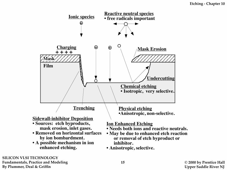
Reactive neutral species• free radicals importantIonic species
+
+ + + + Mask Erosion
Sidewall-inhibitor Deposition• Sources: etch byproducts, mask erosion, inlet gases.• Removed on horizontal surfaces by ion bombardment.• A possible mechanism in ion enhanced etching.
Charging
Trenching
Ion Enhanced Etching• Needs both ions and reactive neutrals.• May be due to enhanced etch reaction or removal of etch byproduct or inhibitor.• Anisotropic, selective.
Undercutting
+ +
Chemical etching• Isotropic, very selective.
Physical etching•Anisotropic, non-selective.

Etching - Chapter 10
SILICON VLSI TECHNOLOGYFundamentals, Practice and ModelingBy Plummer, Deal & Griffin
© 2000 by Prentice HallUpper Saddle River NJ
16
Models and SimulationReactive neutral
("chemical") speciesIonic species +
MaskFilm
Emitted ordesorbed flux
Deposited species+
Resputtered flux
Redepositedor readsorbed
flux
• There is a great deal of similarity between the deposition models described in Chapter 9 and etching models.• Both use incoming "chemical" (neutral) and ion fluxes and many other similar physical processes.
Surface of wafer
Arrival angledistribution at a plane
just above surface
Gas phase
• As in deposition, the etch rate is proportional to the net flux arriving at each point.• Chemical etching species are assumed to arrive isotropically (n = 1 in ).• Ionic species are assumed to arrive anisotropically (vertically) (n ≈ 10 - 80 in ). • The "sticking coefficient" concept is used as in the deposition case. Ionic species usually "stick" (Sc = 1), while reactive neutral species have low Sc values (bounce around).• Sputtering yield has same angle dependence used in the deposition case.
�
cosn θ
�
cosn θ

Etching - Chapter 10
SILICON VLSI TECHNOLOGYFundamentals, Practice and ModelingBy Plummer, Deal & Griffin
© 2000 by Prentice HallUpper Saddle River NJ
17
Linear Etch Model
• While machine specific models have been developed, we will consider here general purpose etch models which can be broadly applied.• Linear etch model assumes chemical and physical components act independently of each other (or appear to act independently for a range of conditions).
(7)
• Fc and Fi are the chemical flux and ionic flux respectively, which will have different incoming angular distributions and vary from point to point. Ki and Kf are relative rate constants for two components.• Physical component (2nd term) can be purely physical sputtering, or can be ion-enhanced mechanism in regime where chemical flux not limiting ion etching.
�
Etch rate =ScKfFc + KiFi( )
NŒ�1cú �11Œ�1cú �11Œ�11ú �11Œ�1cc�1cŒ�1cŒ�1cŒ�11c�1cc
-0.5 0.50.0 1.0-1.0
-0.5
0.0
0.5
1.0
microns
microns
Œ�1cú �11Œ�1cú �11Œ�11ú �11Œ�1cc�1cŒ�1cŒ�1cŒ�11c�1cc
-0.5 0.50.0 1.0-1.0
-0.5
0.0
0.5
1.0
microns
microns
Œ�1cú �11Œ�1cú �11Œ�11ú �11Œ�1cc�1cŒ�1cŒ�1cŒ�11c�1cc
-0.5 0.50.0-1.0
-0.5
0.0
0.5
1.0
microns
microns
1.0
a). all chemical etching (ion flux=0); b). all physical or ionic etching (chem flux=0); c). half chemical, half physical.

Etching - Chapter 10
SILICON VLSI TECHNOLOGYFundamentals, Practice and ModelingBy Plummer, Deal & Griffin
© 2000 by Prentice HallUpper Saddle River NJ
18
Saturation - Adsorption Etch Model
• Used for ion-enhanced etching, when chemical (neutral) and physical (ion) etch components are coupled.• Examples - the ion flux is needed to remove a byproduct layer formed by the chemical etching, or ion bombardment damage induces chemical etching.
�
Etch Rate = 1N
11
KiFi+ 1
ScFc
⎛
⎝ ⎜
⎞
⎠ ⎟
(8)
ˇ�����ˇˇˇ �ˇˇˇ �ˇˇˇ �ˇˇ �̌ˇˇˇ �����ˇˇˇ �ˇˇˇ �ˇˇˇ �ˇˇˇ �ˇˇˇ �ˇˇ �̌����ˇˇˇ �ˇˇˇ �ˇˇˇ �����ˇˇˇ �����ˇˇˇ �ˇˇˇ �����ˇˇ �̌ˇˇˇ �����ˇˇˇ �ˇˇˇ �����ˇˇˇ �����ˇˇˇ �ˇˇˇ �����ˇˇ �̌ˇˇˇ �ˇˇˇ �ˇˇˇ�ˇˇˇ�ˇˇˇ�ˇˇˇ�����ˇˇˇ�����ˇˇˇ�ˇˇ �̌ˇˇˇ�ˇˇˇ�����ˇˇˇ�ˇˇˇ�����ˇˇˇ�ˇˇˇ�ˇˇˇ�����ˇˇˇ�ˇˇˇ�����ˇˇˇ �����ˇˇˇ�ˇˇˇ��
0
0.2
0.4
0.6
0.8
1
0 0.5 1 1.5 2 2.5 3 3.5 4Ion flux • Ki
Etch
rat
e
Chem. flux • Sc = 1
= 0.5
= 0.2
= 0
• If either flux is zero, the overall etch rate is zero since both are required to etch the material.• Etch rate saturates when one component gets too large relative to the other (limited by slower of two series processes). • General approach with broad applicability. (But does not account for independently formed inhibitor layer mechanism, and does not model excess inhibitor formation.)

Etching - Chapter 10
SILICON VLSI TECHNOLOGYFundamentals, Practice and ModelingBy Plummer, Deal & Griffin
© 2000 by Prentice HallUpper Saddle River NJ
19
Œ�1cú �11Œ�1cú �11Œ�11ú �11Œ�1cc�1cŒ�1cŒ�1cŒ�11c�1cc
-0.5 0.50.0-1.0
-0.5
0.0
0.5
1.0
microns
microns
1.0
(a) (b)
• SPEEDIE simulation (equal chemical and ion components): Note the anisotropic etching. Ion flux is required and it arrives with a vertical direction (n is large in ).
�
cosn θ
• Avant!’s TAURUS-TOPOGRAPHY simulation using their dry etch model with simultaneous polymer deposition.• a). Etching SiO2 (over Si, with a photoresist mask) after 0.9 minutes; b). after 1.8 minutes. • This explicitly models inhibitor deposition and sputtering.• One can see the sloped etch profile, without etch bias, due to the excess polymer deposition.

Etching - Chapter 10
SILICON VLSI TECHNOLOGYFundamentals, Practice and ModelingBy Plummer, Deal & Griffin
© 2000 by Prentice HallUpper Saddle River NJ
20
Summary of Key Ideas
• Etching of thin films is a key technology in modern IC manufacturing.• Photoresist is generally used as a mask, but sometimes other thin films also act as masks.• Selectivity and directionality (anisotropy) are the two most important issues. Usually good selectivity and vertical profiles (highly anisotropic) are desirable. • Other related issues include mask erosion, etch bias (undercutting), etch uniformity, residue removal and damage to underlying structures.• Dry etching is used almost exclusively today because of the control, flexibility, reproducibility and anisotropy that it provides.• Reactive neutral species (e.g. free radicals) and ionic species play roles in etching.• Generally neutral species produce isotropic etching and ionic species produce anisotropic etching.• Physical mechanisms:
• Chemical etching involving the neutral species.• Physical etching involving the ionic species.• Ion-enhanced etching involving both species acting synergistically.
• Simulation tools are fairly advanced today and include models for chemical, physical and ion-enhanced etching processes.• Incoming angular distributions of etching species and parameters like sticking coefficients are used to model etching (similar to deposition modeling).


![+9 Swift Heavy ion Irradiation: Augmented Removal of ... IJTAS-4-2017-SUKRITI.pdf · etching, electron beam and ion beam irradiation [9-10]. Ion beam irradiation due to its intense](https://img.pdfslide.us/doc/110x75/5e1eb1dbc6517250c168f9c4/9-swift-heavy-ion-irradiation-augmented-removal-of-ijtas-4-2017-sukritipdf.jpg)