Embed Size (px)
Citation preview

Etching and XRay Topography of FluxGrown Magnetic GarnetsRoger F. Belt Citation: J. Appl. Phys. 40, 1644 (1969); doi: 10.1063/1.1657826 View online: http://dx.doi.org/10.1063/1.1657826 View Table of Contents: http://jap.aip.org/resource/1/JAPIAU/v40/i4 Published by the American Institute of Physics. Additional information on J. Appl. Phys.Journal Homepage: http://jap.aip.org/ Journal Information: http://jap.aip.org/about/about_the_journal Top downloads: http://jap.aip.org/features/most_downloaded Information for Authors: http://jap.aip.org/authors
Downloaded 12 Apr 2013 to 171.67.34.69. This article is copyrighted as indicated in the abstract. Reuse of AIP content is subject to the terms at: http://jap.aip.org/about/rights_and_permissions

JOURNAL OF APPLIED PHYSICS VOLUME 40, NUMBER 4 15 MARCH 1969
Etching and X-Ray Topography of Flux-Grown Magnetic Gamets*
ROGER F. BELT
Airtron Division, Litton Precision Products, Inc., Morris Plains, New Jersey 07950
(Received 17 July 1968; in final form 12 November 1968)
Internal gr~)\,:th defects of high-qu~lity garnet crystals were studied by selective etchants and Lang x-ra~ .transnusslOn topography. Ternunal growth sections contained the fewest defects and dislocation densIties were 10LlO4jcm2. Intern.al sections revealed both randomly dispersed etch pits and linear arrays. The latter were frequently .found In the form of parallel grids. Results indicated that {100}, {111}, {411}, and (lOS) were the defectIve planes. X-ray topographs verified that parallel linear faults are present in crystals on 0~se ?ame planes. The fa~~ts are not dislocation lines but tubular structural deviations caused by flux precIpItat~on or other composItIonal changes. The origin and arrangement of the internal faults are ~elated to fl~ctuatlOns of the crystal growth rate. The rate changes can be initiated by small thermal gradients m the solution.
I. INTRODUCTION
High-quality single-crystal garnets of centimeter size are desirable for many proposed magnetic, optical, and acoustic applications. These crystals are commonly grown by the Czochralskil method if-congruently melting, from appropriate fluxes2 if incongruently melting, or a combination of the good features of both methods.8,4 Unfortunately, local growth variables may lead to unique faults in the crystals, even among those grown by the same method. The purpose of this paper is to examine defects in some flux-grown crystals of yttrium iron garnet (YIG) and yttrium iron gallium garnet (YIGaG). These defects may contribute to observed variations of physical properties in bulk crystals.
Defects in crystals can be directly revealed by many techniques. Chemical etchants provide a simple and rapid estimate of the relative perfection of single crystals. The application of selected reagents to YIG single crystals was first reported by Ramsey.5 Imperfections in slices were later studied by Lefever, Chase, and Torpy; using cold HCl. In a subsequent article,7 the application of HaP04 on {211} and {110} faces was mentioned. Details were not given and estimates of dislocation contents were not made. The most thorough analysis of etching behavior on YIG was performed by Hanke.s She perfected dilute H2S04, dilute HCI, aqua regia, a HNOa-CHaCOOH-H20 mixture, and a H2SOC
H2C20 4 mixture. Dislocation densities were in the range of lOL 106/cm2• The growth of YIG from flux systems suggested that the latter could also serve as etchants. Such a system of PbO-B20 a was proposed by Remeika.9
* A portion of this work was supported by the Air Force Materials Laboratory, Manufacturing Technology Division (MATE), Wright-Patterson Air Force Base, Ohio.
1 J. Czochralski, Z. Phys. Chern. 92, 219 (1918). 2 J. W. Nielsen, J. Appl. Phys. 29, 390 (1958). 3 R. C. Linares, J. Appl. Phys. 35, 433 (1964). ~ M. Kestigian, J. Amer. Ceram. Soc. 50, 165 (1967). "T. H. Ramsey, J. Amer. Ceram. Soc. 42,645 (1959). 6 R. A. Lefever, A. B. Chase, and J. W. Torpy, J. Amer. Ceram.
Soc. 44, 141 (1961). 7 R. A. Lefever and A. B. Chase, J. Amer. Ceram. Soc. 45, 32
(1962) . 8 I. Hanke, Z. Angew. Phys. 14, 465 (1962); 14, 557 (1962). 9 J. P. Remeika, U.S. Patent 3063886 (1962).
X-ray transmission topography as developed by LanglO is suitable for studying internal defects of large areas of a high quality crystal. Dislocations, precipitates, magnetic or ferroelectric domains, and other structural changes have been directly revealed. Some recent applications to garnets have included magnetic domain configurations in terbium iron garnetll and YIG.I2 Core damage of laser crystals was studied in yttrium aluminum garnet.Ia
II. EXPERIMENTAL
Single crystals of YIG and YIGaG were grown from a PbO-PbF2 flux. B20 a was added in some cases. The crystals were initially cleaned in a HNOa-CHaCOOH mixture. Selected crystals were cut with a diamond wheel to obtain slices parallel to {100), \110}, and { 111} faces. Orientation was performed by Laue x-ray back-reflection methods. The area of a face was 0.5-1.0 cm2• Mechanical polishing was accompolished with successively finer grits of SiC papers. A terminal operation utilized 2 JLm AbOa in a water slurry to obtain a highly polished and scratch free surface. Previous experience in these laboratories with the use of 85% HaP04 on ferritesI4 has led to applications with YIG single crystals. By a judicious choice of time and temperature, HaP04 may act both as a polishing agent and a dislocation etchant. The chemical polishing and etching were performed in HaP04 at temperatures of 100°-100°C and times of 10-45 min. Hot concentrated HCI was also utilized to confirm results obtained from the HaP04•
Topographs were obtained by transmission on a Rigaku Denki Lang camera. A standard target x-ray tube was used as the source. The source-to-sample distance was fixed at 50 cm and the beam was collimated
10 A. R. Lang, Acta Cryst. 12, 249 (1959); J. Appl. Phys. 30, 1748 (1959).
11 J. Basterfield and M. J. Prescott, J. Appl. Phys. 38, 3190 (1967) .
12 J. R. Patel, K. A. Jackson, and J. F. Dillon, Jr., J. Appl. Phys. 39, 3767 (1968).
13 J. Basterfield, M. J. Prescott, and B. Cockayne, J. Mater. Sci. 3,33 (1968).
14 D. A. Lepore, R. F. Belt, and J. W. Nielsen, J. Appl. Phys. 38, 1421 (1967).
1644
Downloaded 12 Apr 2013 to 171.67.34.69. This article is copyrighted as indicated in the abstract. Reuse of AIP content is subject to the terms at: http://jap.aip.org/about/rights_and_permissions

ETC HI N G AND X - RAY TOP 0 G RAP H Y 0 F MAG NET leG A R NET S 1645
with 0.15 mm slits. The resulting divergence in a horizontal plane was 100 sec. The divergence in the vertical plane was about 2°. Based on these conditions the horizontal resolution was approximately 1 ,urn and the vertical resolution was about 8 ,urn. Kodak type A autoradiographic plates and Ilford nuclear plates, emulsion G5, were used for recording the topographic images. Exposure times were 0.5 to 1.0 hjmm of scan length.
For the proper observation of defects using the transmission method of Lang, it is desirable that the product ,ut (,u=linear absorption coefficient, t=thickness) have a value of about one. For AgKa radiation used in our present experiments, ,u=143 cm-l and t is 0.007 cm. The preparation of thin slices of YIG was accompolished by mechanically abrading to a thickness of 0.25 mm. The finer grits of SiC papers were utilized to obtain a smooth surface. Final mechanical polishing was performed with 0.3 ,urn Linde AbOa. To remove surface damage and thin the YIG crystals to under 0.01 cm, it was necessary to utilize HaP04 at temperatures of 200°-300°C. Under these conditions, a chemically polished defect free surface can be obtained.
III. RESULTS AND DISCUSSION
A. Etching Studies of Low Index Faces
All of the crystals possessed the characteristic garnet morphology, i.e., prominent {110) and {211) faces. These faces are usually of the highest perfection because later growth occurs under near equilibrium conditions. However, the entire crystal must be considered with respect to its growth history. It is more frequently found that a large crystal with perfect faces has many obvious defects when cut open. The most likely are flux inclusions easily visible under the microscope. Examples and photographs are given in two papers.6 ,7
Our primary concern in this paper is not with these gross inclusions, but with internal defects that cannot be immediately seen unless further processed by etching or examined by x-ray topography.
In etching the principal faces of a YIG crystal, characteristic pits are formed. These pits have been attributed to dislocations whose density may range from lOL 105jcm2. Such a range in density is not uncommon but adequate proof has never been presented that only dislocations were being etched. It was tacitly assumed in many reports, that etch pits formed where dislocation lines intersected the surface. This behavior is not unique to a dislocation line, but may be caused by other phenomena such as impurity precipitation, phase segregation, and fission tracks. In the following Sections, evidence is presented to show that some flux-grown YIG and YIGaG contain etchable interior defects which are not likely dislocations.
Figure 1 (a) shows the surface obtained from the etching of a (100) face. Both hexagonally rounded and square pits were found with a density of about 104/cm2.
The former were sometimes arranged in rows along (110) suggesting a small-angle boundary or parallel defects of another type. Figure 1 (b) is the micrograph of a (110) surface and shows characteristic diamondshaped pits (black areas) with an approximate density of 5X10³jcm2• The background consists of a nearly complete covering of diamond-shaped hillocks. Figure l(c) is a similarly etched (111) face with triangularly shaped pits. An upper limit of the density is 5X 104 cm2. Figure 1 (d) is an etched (211) face with a pit density of 10ajcm2. While the results of Fig. 1 were all obtained with HaP04, it was discovered that concentrated HCI, aqua regia, and other etchants8 gave similar results. It was also noticed that the {110) and {211) sections consistently gave lower etch-pit densities. Some of these were as low as 102jcm2.
B. Internal Parallel Bands of Etchable Defects
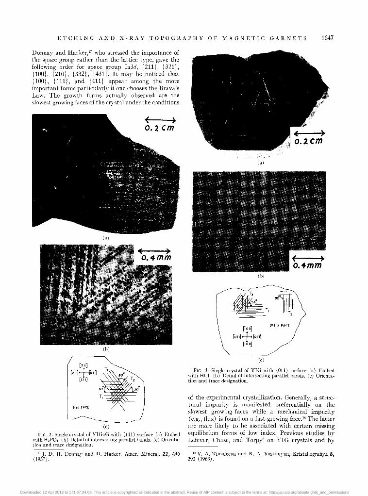
During the preparation of thin slices for x-ray topography, many YIG and YIGaG crystals were sectioned and found to be free of interior flux inclusions. The quality of internal crystal sections persisted during mechanical polishing. However, when reagents were applied for chemical polishing, groups of defects were revealed. Figure 2(a) is a photograph of a (111) surface of a YIGaG crystal etched with HaP04• The etching revealed one region at the right, which was heavily covered with parallel bands of defects. The remainder of the crystal was free of defects except for a few pits and small irregular lines of flux inclusions. Figure 2 (b) is the same crystal under high magnification. It shows the intersections of two systems of bands. The included angle on the (111) surface was 50 0 ±2°. Figure 2(c) is a line drawing of the crystal face illustrating the orientation of the parallel bands with respect to natural growth faces and other directions. The angles between the traces on the surface for systems Tl , T2, and Ta are also given.
Consideration was now given to systems found on other planes. Figure 3(a) is a photograph of a YIG crystal whose interior (011) face was etched with HC!. Distinct areas of parallel linear defects occurred only in select areas. Out near the natural growth faces the crystal was of better quality and free of the linear type defects. Figure 3 (b) gives a detailed view of the defects. Figure 3(c) is a drawing of the crystal orientation and shows the angles measured between the traces on the surface. Finally, YIGaG crystals were cut to expose major {001) faces. Figure 4(a) is the etched surface and Fig. 4(b) shows a more detailed view. For defects on (001) the formation of neat geometrically shaped pits was more difficult. This behavior was clearly related to directional effects of etching and how the defects lie. Again, the bands of defects formed three systems of traces. The orientation of the crystal and the traces are presented in Fig. 4(c).
To identify the planes on which the defects lie, crystals were cut in a manner such that the surface was
Downloaded 12 Apr 2013 to 171.67.34.69. This article is copyrighted as indicated in the abstract. Reuse of AIP content is subject to the terms at: http://jap.aip.org/about/rights_and_permissions

1646 ROGER F. BELT
(a) (b)
(c) (d)
FIG. 1. Single crystals of flux-grown YIG etched in 85% HaPO., 5-30 min at 15Q--200°C, random etch pits developed; (a) (100) face, (b) (110) face, (c) (111) face, (d) (211) face.
90° to the etched face, and likewise 90° to the parallel trace lines of defects. Thus, if the defects truly lie in a plane, the plane's trace should also be evident on any newly exposed face. For some of the traces, the exposed plane was parallel to a growth face of {211) or {11 0) type. This greatly assisted in any further identification. The newly cut face was polished and etched as before. The traces on the new face were verified and could be assigned to certain planes. Furthermore, the angles of intersection of the traces were readily measured. Therefore it was possible to actually designate the plane of defects from its traces on two other known planes.I5 A summary of the data is given in Tables IIII for the traces found on each major surface.
From the data of Tables I-III, a general pattern is evident. Most of the defects tend to lie on {100) planes and {1111 planes. In cases where there are other types of planes observed, e.g., {lOS I or (411), the planes are close to {100). Accordingly, these could be of vicinal type. Some additional facts are also pertinent for all
15 For details on the principles and analytic constructions with the stereographic projection, reference is made to C. S. Barrett Structure of Metals (McGraw-Hill Book Co., New York, 1952), p.42.
of the crystals having bands of defects. The major concentration of defects appears near the centers or nucleation points of the crystal. The defects also apparently end within the volume of the crystal. Few or no defects were observed on the growth faces of crystals and not all flux-grown crystals contained the defects. Crystals were examined from different growth fluxes, the same flux, and from pure YIG to substituted YIGaG. As yet, no systematic method has evolved to predict which crystals contain defects of the type described.
A complete solution of the problem involves an identification of the defects plus an explanation of their occurrence on specified planes. The latter question may be partially answered from the growth forms of the garnets. From interfacial angles, it is known that the growth form of the garnets is predominantly {211) and {110). The law of Bravais-FriedeJl6 and its application to a body-centered lattice (other effects negligible) shows the order of importance of the growth form is {110), {100), {211), {31O), {lll), {321), {4ll) •...
16 F. C. Philips, An Introduction to Crystallography (John Wiley & Sons, Inc., New York, 1963), Chap. XIII.
Downloaded 12 Apr 2013 to 171.67.34.69. This article is copyrighted as indicated in the abstract. Reuse of AIP content is subject to the terms at: http://jap.aip.org/about/rights_and_permissions
ETC H I N G AND X - RAY TOP 0 G RAP H Y 0 F MAG NET I C GAR NET S 1647
Donnay and Harker,17 who stressed the importance of the space group rather than the lattice type, gave the following order for space group Ia3d, {211}, {321}, {lOa}, {21O}, {332}, {431}. It may be noticed that {lOa}, {111}, and {411} appear among the more important forms particularly if one chooses the Bravais Law. The growth forms actually observed are the slowest growing faces of the crystal under the c:mditions
(al
(b)
(c)
( > 0.2 em
FIG. 2. Single crystal of YIGaG with (111) surface (a) Etched with H3PO,. (b) Detail of intersecting parallel bands. (c) Orientation and trace design a tion.
17 J. D. H. Donnay and D. Harker, Amer. Mineral. 22, 446 (1937) .
(a)
(b)
(0 II) FACE
(c)
FIG. 3. Single crystal of YIG with (011) surface (a) Etched with HC!. (b) Detail of intersecting parallel bands. (c) Orientation and trace designation.
of the experimental crystallization. Generally, a structural impurity is manifested preferentially on the slowest growing faces while a mechanical impurity (e.g., flux) is found on a fast-growing face. I8 The latter are more likely to be associated with certain missing equilibrium forms of low index. Previous studies by Lefever, Chase, and T orpy6 on YIG crystals and by
18 V. A. Timofeeva and R. A. Voskanyan, Kristallografiya 8, 293 (1963).
Downloaded 12 Apr 2013 to 171.67.34.69. This article is copyrighted as indicated in the abstract. Reuse of AIP content is subject to the terms at: http://jap.aip.org/about/rights_and_permissions

1648 ROGER F. BELT
TABLE I. Data for defects intersecting (111) surface.
Plane traces :\ngle made Plane cut Probable in Fig. 2(c) with (111) at 90° assignment
Tl 35° (011) (411)
T2 60° (110) (ISo)
T3 600 (101) (105)
Giessl9 on Gdl G crystals have verified most of the above principles. The former authors found an initial dendritic stage with (100) and (111) fast growth directions with layered growth parallel to (110 I and {2111. The latter investigator found that preferential growth occurred along [OOlJ with lamellar (100) and (010) dendrites. The defects observed in our studies are very closely allied to those observed by others.6,l9 They are probably related by difference in scale, i.e., our examination was conducted with high-quality crystals containing atomic-size imperfections, while other authors had poorly developed and flux included samples as gathered from published figures.
C. X-Ray Topography of Internal Defects
The direct observation of internal defects can be performed by x-ray diffraction topography. It may be safely concluded that not all etch pits formed by a reagent need be caused by dislocations. Some evidence has been presented that the banded defects observed in flux-grown garnets are not dislocations. Thus, defects ended within the interior or the crystal, they were nearly parallel on certain planes but not evenly spaced, and large regions of pit-free crystal occurred between and adjacent to the defects. This type of behavior is not characteristic of simple dislocations, but may be caused by localized impurities, precipitates, a foreign phase or other minor structural deviation. X-ray topography reveals surface defects and those within the volume of a crystal. However, all types of defects which change the periodicity of the crystal structure over many unit cells are exhibited.
Figure 5(a) is taken from one of our earliest results. This is a transmission topograph recorded with AgKa by means of diffraction from (240) planes. These
TABLE II. Data for defects intersecting (011) surface .
Plane traces .i.ngle made Plane cut Probable in Fig. 3(c) with (011) at 90° assignment
1\ 90° and 20° (otT) !IOO), (100) (411), (411)
T I"" - .) (Too) (001) and (OW)
T3 90° (2 II) (III) and (III)
19 E. A. Giess, J. Amer. Ceram. Soc. 45, 53 (1962).
planes lie 26.5° in a counterclockwise direction from the vertical. The thickness of the crystal was about 50 }Lm. At the left of the topograph are many vertical lines plus three horizontal lines crossing in a 90° grid. All of these were visible on the surface and identical to the grids discussed under the use of chemical etchants. The few
( O.2cm
(a)
(b)
illh
~I~~II~\ [!co)
[Oiq+rOIO]
Doo]
(c)
(001) FACE
. FIG. 4. Single crystal of YIGaG with (001) surface. (a) Etched WIth HaPO,. (b) Detail of intersecting parallel bands. (c) Orientation and trace designation.
Downloaded 12 Apr 2013 to 171.67.34.69. This article is copyrighted as indicated in the abstract. Reuse of AIP content is subject to the terms at: http://jap.aip.org/about/rights_and_permissions

ETC H I N G AND X - RAY TOP 0 G RAP H Y 0 F :VI A G NET I C GAR NET S 1649
,~,"" (a)
( ~ IMM
(b) (c)
FJ(;. 5. Single crystal of flux-grown YIG thinned to SO I'm with HaP04, (00l) major face. (a) X-ray transmission topograph, Ag}'"a, g= [240]. (b) X-ray topograph, g= [040]. (c) Same area of crystal photographed in transmitted light.
at the upper left corner were likewise the same. Now it is evident that there are other defects within the crystal interior that did not etch on the surface. These defects were also manifested as closely spaced linear ones running along [IOOJ [upper right quarter of Fig. S (a)]. From the nature of the x-ray data it is unlikely that the slice possesses any kind of a simple dislocation or stacking fault. For example there are numerous parallel lines that show different widths and considerable variation in contrast. The defect is more characteristic of the flux or a foreign phase precipitating out in random amounts through thermal changes. The planes involved are again perpendicular to fast growth directions.
Figure S (b) is a new topograph from the same crystal. Here, the reflecting planes were (040) and the diffraction vector g was rotated. Most of the features are still present. The major changes are located on the bottom right quarter of the topograph. In this case the contrast of the linear defects directed along [21OJ has become much darker. Furthermore, there is a definite line that intersects the two sets of defects not revealed
TABLE Ill. Data for defects intersecting (001) surface.
Plane traces Angle made Plane cut Probable in Fig. 4(e) with (001) at 90° assignment
1'1 90° (010) (TOO) and (100)
T. 90° (TOO) (010) and (010)
1'" not deter- not definite, but mined {1l1} or {4ll}
likely
by the etching. This line is directed toward [I20J about 26.5° from the horizontal. The explanations of the change in contrast observed on Figs. Sea) and S(b) is difficult, particularly if we are not dealing with dislocations. Some efforts in this direction have been made for particles, precipitates, and elastic strains in crystals.20 Most applications have been studied with electron microscopy or diffraction. Some principles should also hold for x-ray diffraction. The concept of dislocations causing the defects may be partially ruled out because perfect dislocations in bcc lattices have Burgers vectors of HIll) and (100) type. Imperfect dislocations and twins have also i (112) or i (111) Burgers vectors. These simple Burgers vectors do not account for the observed contrast.
Figure S(c) is a photograph of the identical crystal used to obtain the topographs of Figs. S (a) and S (b). This photograph was taken by means of transmitted light. The etched defects appears as lines of low transmission because of reflection and scattering losses. If slices of YIG are polished to the same thickness and not etched, it is not possible to see the defects described here. Truly, the imperfections are to be considered as submicroscopic in character and are similar to dislocations. On Fig. 5 (b), there are areas containing linear defects that did not etch, and yet the defects are clearly visible on the x-ray topographs. One explanation is that these defects are totally within the interior of the crystal and thus unaffected by the chemical reagent.
Crystals of VaFeuGaO.7012 were also examined and results were similar to those obtained with pure VIG.
20 P. B. Hirsch, A. Howie, R. B. Nicholson, D. W. Pashley, :\1. J. \Vhelan, ]iZectron Microscopy oj Thin Crystnls (Butterworths Scientific Publications, Inc., \Vashington, 1965), Chap. 14.
Downloaded 12 Apr 2013 to 171.67.34.69. This article is copyrighted as indicated in the abstract. Reuse of AIP content is subject to the terms at: http://jap.aip.org/about/rights_and_permissions

1650 ROGER F. BELT
(a)
Slices were prepared parallel to major (100) faces. The x-ray transmission topograph is shown in Fig. 6(a). The major directions in the (100) plane are illustrated on the photograph. Internally the crystal showed the same type of defects as found in pure YIG. A fine parallel system of lines runs along an [OlOJ direction. These lines are located at the left side of the picture 45° from the horizontal and are the most prominent. It was strongly suspected that the defects lie on (1001 type planes, and intersected the surface at right angles. Other more diffuse parallel bands are located on Fig. 6(a). These are mainly near the top center and at the lower right corner. Both of these systems lie along (210) directions in the (100) plane. The contrast is very weak compared to the lines along [010]. This suggests that the Burgers vectors of the two systems are different and that the variation in contrast may be caused by the particular orientation of the diffraction vector g.
To check the above possibility, the same crystal was rotated in its plane 45° clockwise. A new topograph was taken from (040) planes. The results are shown in Fig. 6(b). Again, the parallel lines in the bottom left corner have the best contrast. These were directed along [010]. The bands at the lower right corner were now highly visible, while those in the top center were missing. Several other topographs were taken with new diffraction vectors and contrast changed in these topographs. All of the topographs are not shown here, but review of the data can lead to some conclusions. In column one of Table IV are listed the directions of several alternate diffraction vectors obtained by rotating the slice in its own (100) plane. Column two lists the approximate relative contrast for the particular defects that lie along the specific directions. High contrast for a defect occurs when the scalar product g. b= 1. Little or no contrast appears for g·b=O. With these criteria in mind and the observations of Table IV, strain vectors of (001) and (111) are possible. This does not mean
(b)
FIG. 6. Single crystal of fluxgrown YIGaG 120 "m thick, (100) major face. (a) X-ray transmission topograph, AgKa , g=[088J. (b) Same crystal with g= [040].
that perfect dislocations were present. On the contrary, the nature, arrangement, and behavior under thermal treatment all suggests a different defect than a dislocation.
III. DISCUSSION
The nature of the defects described suggest phenomena associated solely with the growth process. Dislocations can be introduced into solution grown crystals by processes such as epitaxial growth on seeds, plastic
TABLE IV. Contrast as a function of diffraction vector, g, for defects observed on (100) plane.
Direction of diffraction
vector g
[OllJ
Relative contrast of defects for
listed direction
[Ol1J strong
[021J medium
[021] weak
[021J [Ol1J medium
[021J weak
[021J medium
[OlOJ [OllJ weak
[021J weak
[021J strong
[01I] [Ol1J medium
[021J strong
[021J weak
[OOIJ [011 J strong
[021J weak
[02I] strong
Downloaded 12 Apr 2013 to 171.67.34.69. This article is copyrighted as indicated in the abstract. Reuse of AIP content is subject to the terms at: http://jap.aip.org/about/rights_and_permissions

ETC H I N G AND X - RAY TOP 0 G RAP H Y 0 F MAG NET I C GAR NET S 1651
deformation, interfacial connection of nuclei, and stresses caused by variations of the concentration gradient. The low dislocation contents observed on growth faces, absence of grain boundaries, and presence of linear arrays suggest the concentration gradient mechanism as a likely process for flux-grown crystals. This may be coupled with nonuniform thermal gradients occurring throughout the solution. The latter arise from variations in furnace control over the extended growth times involved. Surface features on flux grown garnets such as hillocks, spirals, and steps indicate that terminal growth is associated with dislocations having a screw component,7 These dislocations likely originate from impurities which change the lattice parameter of the crystal and lead to strain and misfit regions. X-ray topographs clearly reveal some of these dislocations that lay perpendicular to /2111 and 11101 growth faces. However, other defects are parallel to the growth faces and these must possess an edge component.
The problem of the linear arrays of etch pits observed principally in the interior or large crystals is more complicated. Impurity banding,6 tube formation,7 and striations21 have been observed in flux-grown garnets and other materials. Our results are analogous to these but are on a much smaller scale. The precipitation of a foreign phase, diffusion into dislocations, and sharp concentration gradients have been suggested as causes. The onset of the phenomena is directly related to temperature fluctuations in the melt. In certain systems, the addition of selected impurities may reduce growth strains or diminish the striation problem.22 ,23 A complete elimination is relatively difficult in large, centi-
21 A. B. Chase and W. R. Wilcox, J. Amer. Ceram. Soc. 50, 332 (1967).
22 A. B. Chase and H. H. Tippins, J. Appl. Phys. 38, 2469 \1967).
23 R. A. Lefever, K. A. Wickersheim, and A. B. Chase, J. Phys. Chem. Solids 26, 1529 (1965).
meter size crystals. There are not many systems in which the absence of striations has been demonstrated by x-ray topography. This technique is one of the most sensitive methods. Some optical techniques may not detect the striations unless refractive index changes or associated strains are large enough.
IV. CONCLUSIONS
Flux-grown garnets exist as very perfect crystals with dislocation contents as low as 102-103/cm2•
Etching studies with HaP04 and Hel show that the lowest defect densities are found on the natural growth faces or sections in their vicinity. The interiors of some large crystals contain not only visible flux inclusions, but also microscopic etchable parallel bands of defects. The bands are composed of linear tubelike structures which define certain planes in the crystals. The planes were identified from their traces on known surfaces of intersection. The defects are located principally on fast growth 1100 I and 11111 type planes, which are easily susceptible to impurity precipitation and thermal effects. The microscopic interior defects were also directly revealed by means of Lang x-ray transmission topography. Some defects possessed the properties of ordinary dislocations. Their possible Burgers vectors were (001) and H111) as derived from contrast data. Such data may not be completely valid for the defects that formed bands. Impurities and strain may lead to the unique arrangement and properties. The defects can be initiated by small thermal fluctuations throughout the growth solution.
ACKNOWLEDGMENTS
The author thanks D. Leo for providing crystals from a variety of growth conditions. The careful sample preparations were performed by J. Moss.
Downloaded 12 Apr 2013 to 171.67.34.69. This article is copyrighted as indicated in the abstract. Reuse of AIP content is subject to the terms at: http://jap.aip.org/about/rights_and_permissions