Embed Size (px)
Citation preview
Establishing Programmable Josephson Voltage
Standard and Maintaining Its Quantum Accuracy
Tezgül Coşkun Öztürk1, Sarp Ertürk
2, Ali Tangel
2, Adem Gedik
1, Mesut Yoğun
1, and Murat Celep
1
1 TÜBİTAK Ulusal Metroloji Enstitüsü, P.K. 54, 41470, Gebze-Kocaeli, Turkey
2 Kocaeli Üniversitesi, Müh Fak, Elektronik ve Haberleşme Müh, Umuttepe Yerleşkesi, 41380, İzmit-Kocaeli, Turkey
Email: tezgul.ozturk; adem.gedik; mesut.yogun; [email protected]; serturk; [email protected]
Abstract—In this article, programmable Josephson voltage
standard system established in TÜBİTAK UME is presented.
The specifications of the instruments used in the system are
defined and tested according to the needs of the system. Test
setups are given in detail. The cryoprop used to immerse the
superconducting integrated circuit into the liquid helium is
manufactured. The horn antennas used in the waveguide
part of the cryoprop are manufactured by employing wire
erosion technique. The optical transceivers having low jitter
for distributing trigger and clocks while keeping fully
floating the system are manufactured. The software for
generating quantum voltages and easy use of the system is
prepared and equations used in the algorithm are given.
The procedures to maintain the necessary accuracy of the
bias electronics to maintain the quantum accuracy of the
system is given in detail. The established system is used in
metrological measurements and the results of the
measurements which prove the quantum state of the system
are presented.
Index Terms—voltage, Josephson voltage standards, DAC,
ADC static gain, dynamic gain
I. INTRODUCTION
In 1962, Brain Josephson predicted the intrinsic
behavior of the cooper pairs when they are tunneled
through a thin barrier of insulator installed between two
super conductors [1], and in 1963, his theory was proven
[2], [3]. In the following years, many experiments [4]
have been performed to prove the frequency voltage
relation in which voltage and frequency are proportional
by multiplication of physical constants and an integer.
Several experiments have shown that the equation is
independent from the geometry and material of the
junction, power of the microwave and magnetic field [4].
The presence of such an equation promises the voltage
agreement at the accuracy and stability of the frequency
quantity.
The proof of this equation encouraged metrologists to
measure 2e/h constant which is known as Josephson
constant (KJ). The present value of KJ was accepted in
1990 and denoted by KJ-90 after a comparison which has
0.4 ppm uncertainty [5], [6]. Despite of this absolute
Manuscript received January 15, 2018; revised March 1, 2018;
accepted June 20, 2018. Corresponding author: Tezgül Coşkun Öztürk (email: tezgul.ozturk
@tubitak.gov.tr)
uncertainty, accepting a conventional value for KJ-90
improved the voltage unity in the world firstly to 0.01
ppm level with single JJ and to 0.001 ppm level with
arrays of JJs [7].
Connecting the JJs serially was possible in 1981 using
underdamped JJs because of the lack of JJs with the same
electrical attributes. With underdamped JJs, it is possible
to generate VJ, while the dc current is zero for the all
voltage steps, for n=0, ±1, ±2, ±3, ⋯ [8]. These DC zero
current crossing voltage steps were enabling technology
for Josephson voltage standards (JVS) and mostly called
as conventional JVS while they had intrinsic and
unwanted two disadvantages: 1) Changing rapidly
between different steps was not possible and 2) noise
sometimes could change the steps randomly [7].
In 1995, another kind of JVS having voltage steps,
which are stable and programmable by changing the dc
current, called as programmable JVS (PJVS), was
suggested [7]. In this standard, JJs are over dumped and n
is 0 or ±1. Different quantum voltages are selected by
changing the dc current of the arrays of JJs divided into
segments. This standard over comes the two
disadvantages of the Conventional JVSs and moreover
enables the dynamic measurements of DAC&ADCs at
low frequencies. This technology was not possible in
1980s, but in 1995, this was possible because of the
developments in junction manufacturing and on chip
microwave power distributing technologies [7].
JVSs are the basis of electrical metrology [9], [10].
More than one PJVS system is necessary to disseminate
quantum accuracy to electrical quantities. Instead of
buying a ready system, TÜBİTAK UME preferred to
establish its own system. This has the advantage of
interchanging the parts of the system and establishing
different setups using the PJVS systems.
In this study the established system is presented. The
hints to keep the system at quantum state are addressed.
II. COMPONENTS OF THE SYSTEM
The heart of PJVS is the superconducting integrated
circuit (SIC) consisting of over dumped JJs and
distributed microwave architecture [11]. The Josephson
voltage across one JJ is given in (1).
2J
nfhV
e (1)
International Journal of Electrical and Electronic Engineering & Telecommunications Vol. 8, No. 1, January 2019
19©2019 Int. J. Elec. & Elecn. Eng. & Telcomm.doi: 10.18178/ijeetc.8.1.19-25
where VJ is the voltage across the barrier when the super
conducting Josephson Junction (JJ) is biased with
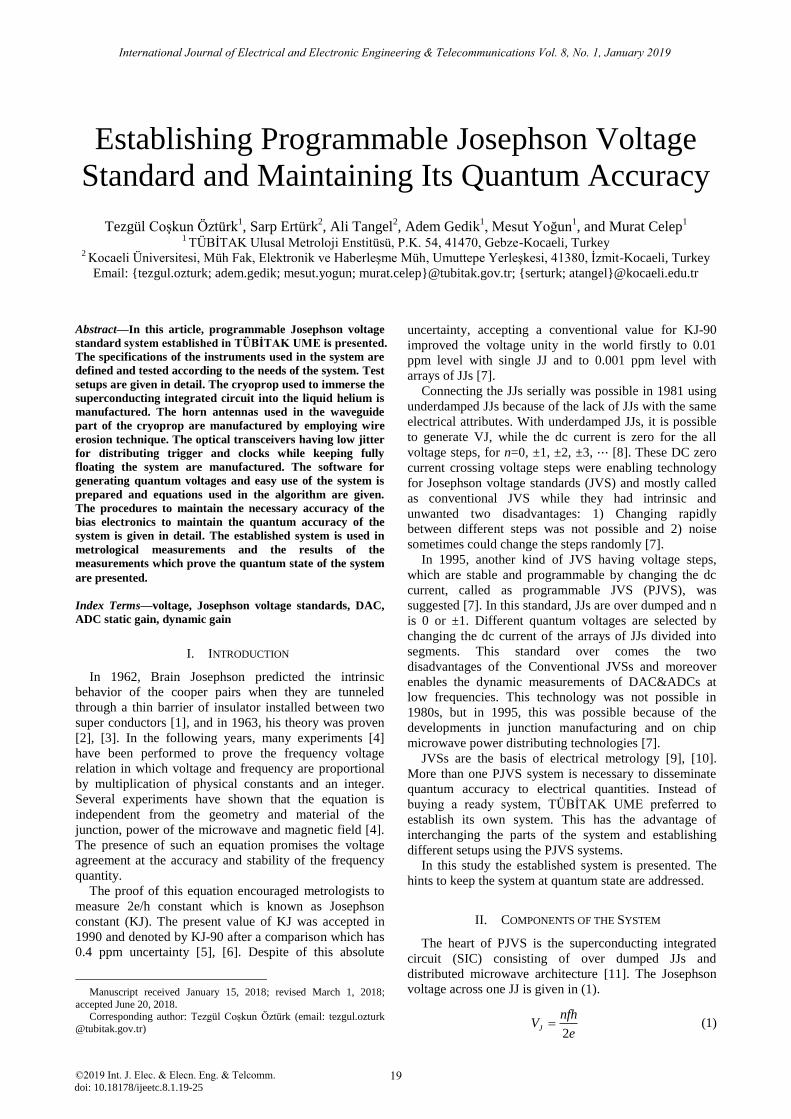
appropriate dc and ac currents as illustrated in Fig. 1 [7]. f
is the frequency of the AC current applied through the
junction. h and e are the plank and the electron charge
constants respectively and n is an integer.
The integrated circuit is borrowed from PTB within
cooperation in Q-Wave and QuADC [12] projects. The
integrated circuit has Nb as a super conductor. The
temperature of superconductivity of Nb is 9.2 K. The
temperature environment below 9.2 K is provided by
liquid helium in a Dewar. A Dewar is a container which
consists of nested cups with an outer layer of vacuum and
liquid helium in the inner layer. The temperature at which
the helium gas is fluidized is 4.2 K. The integrated circuit
on a carrier shown in Fig. 2 is immersed in a liquid
helium, via a so-called cryoprop.
The task of the cryoprop is to transmit microwaves and
± In currents shown in Fig. 1, as well as immersing the
chip in liquid helium. The microwave source applies the
high frequency AC signals shown in Fig. 1. The
microwave power required at the antenna of the SIC for
stable operation of the steps is around 50 mW. To lock
the phase of the microwave source and thus to increase
the frequency accuracy, a high-stability rubidium or
cesium oscillator is used.
Fig. 1. Biasing Josephson junctions [7].
Fig. 2. Established PJVS system.
A magnetic shield is used to prevent the
superconductivity from being affected by the external
magnetic fields. The dc current illustrated in Fig. 1 is
provided by the bias electronics. Each of the ± In currents
shown in Fig. 1 is provided by DACs with voltage output
that form the bias electronics.
The PJVS voltage needs to be "floating": For this
reason, the synchronization signals must be converted to
optical signals through the optical "transmitter" and then
back to the electrical signal again via the optical
"receiver". This process is carried out with an optical
transceiver system.
In addition, the system consists of a 28-bit multimeter
(voltmeter) that checks whether the generated voltage is
in quantum step. Software on the computer calculates the
DAC voltage and loads the voltage information into the
DACs and receives the multimeter measurement data.
The communication between the computer and the bias
electronics and the multimeter uses optical hubs produced
for long distance computer communication that helps to
keep the quantum voltage floating. The system is shown
in Fig. 2.
A. Cryoprop
The task of the cryoprobe is to transmit microwave and
low frequency electrical signals to about 1 m between
ambient temperature and superconducting temperature.
The superconducting circuit operates at 68 GHz to 76
GHz. The "oversized" circular waveguide is used for
microwave transmission at this frequency band (E band).
The 'Oversized' waveguide is a waveguide which has
dimensions much larger than the wavelength. Such a
waveguide attenuates the microwave much less compared
to a rectangular waveguide. But the output of the
microwave source and the element that couples the
microwave to the chip is a rectangular waveguide at E
band. An element called converter is a kind of horn
antenna that provides a transition between a rectangular
waveguide and a circular waveguide.
Converters are generally manufactured by
electrolytically collecting copper on the mold. Since the
converters cannot be produced in Turkey with this
technology, the converters used in the system are
produced by employing wire erosion technique. These
converter parts are vital for prop construction. Non-
magnetized, drawn steel tube is used for the waveguide.
Fig. 3 shows the waveguide in the probe.
The insulator shown in Fig. 3 is manufactured to
prevent ground loops by placing a thin Teflon plate
between two of the 1-inch rectangular waveguides with
Teflon screws.
Fig. 4 shows the measurements of attenuation obtained
using the microwave source (millimeter wave
synthesizer--MMWS) and the maximum microwave
power delivered to the probe when using the
manufactured probe and the purchased microwave source.
Fig. 3. Waveguide part of the prop.
Isolator
Waveguide converter
Circular waveguide SIC on the carrier
International Journal of Electrical and Electronic Engineering & Telecommunications Vol. 8, No. 1, January 2019
20©2019 Int. J. Elec. & Elecn. Eng. & Telcomm.
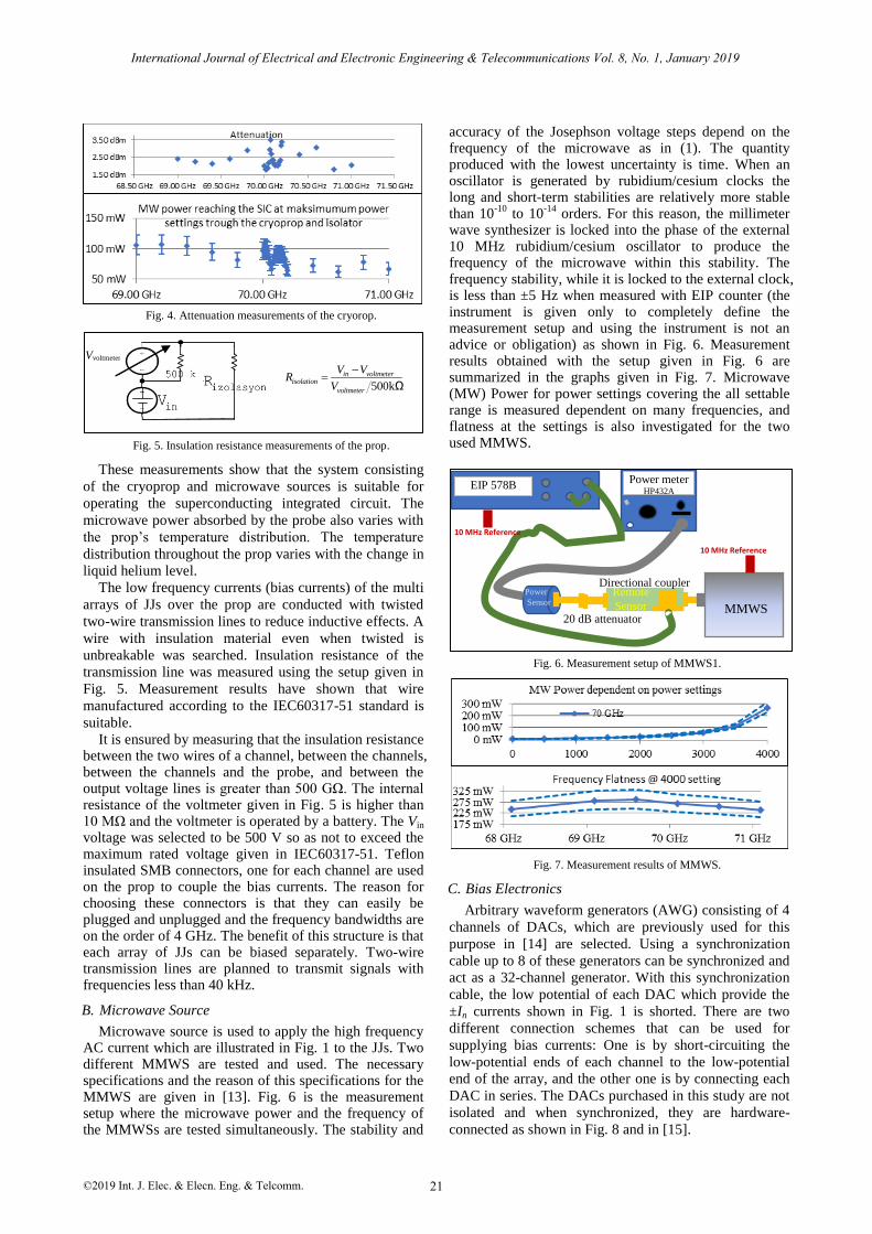
Fig. 4. Attenuation measurements of the cryorop.
Fig. 5. Insulation resistance measurements of the prop.
These measurements show that the system consisting
of the cryoprop and microwave sources is suitable for
operating the superconducting integrated circuit. The
microwave power absorbed by the probe also varies with
the prop’s temperature distribution. The temperature
distribution throughout the prop varies with the change in
liquid helium level.
The low frequency currents (bias currents) of the multi
arrays of JJs over the prop are conducted with twisted
two-wire transmission lines to reduce inductive effects. A
wire with insulation material even when twisted is
unbreakable was searched. Insulation resistance of the
transmission line was measured using the setup given in
Fig. 5. Measurement results have shown that wire
manufactured according to the IEC60317-51 standard is
suitable.
It is ensured by measuring that the insulation resistance between the two wires of a channel, between the channels, between the channels and the probe, and between the output voltage lines is greater than 500 GΩ. The internal resistance of the voltmeter given in Fig. 5 is higher than 10 MΩ and the voltmeter is operated by a battery. The Vin voltage was selected to be 500 V so as not to exceed the maximum rated voltage given in IEC60317-51. Teflon insulated SMB connectors, one for each channel are used on the prop to couple the bias currents. The reason for choosing these connectors is that they can easily be plugged and unplugged and the frequency bandwidths are on the order of 4 GHz. The benefit of this structure is that each array of JJs can be biased separately. Two-wire transmission lines are planned to transmit signals with frequencies less than 40 kHz.
B. Microwave Source
Microwave source is used to apply the high frequency AC current which are illustrated in Fig. 1 to the JJs. Two different MMWS are tested and used. The necessary specifications and the reason of this specifications for the MMWS are given in [13]. Fig. 6 is the measurement setup where the microwave power and the frequency of the MMWSs are tested simultaneously. The stability and
accuracy of the Josephson voltage steps depend on the frequency of the microwave as in (1). The quantity produced with the lowest uncertainty is time. When an oscillator is generated by rubidium/cesium clocks the long and short-term stabilities are relatively more stable than 10
-10 to 10
-14 orders. For this reason, the millimeter
wave synthesizer is locked into the phase of the external 10 MHz rubidium/cesium oscillator to produce the frequency of the microwave within this stability. The frequency stability, while it is locked to the external clock, is less than ±5 Hz when measured with EIP counter (the instrument is given only to completely define the measurement setup and using the instrument is not an advice or obligation) as shown in Fig. 6. Measurement results obtained with the setup given in Fig. 6 are summarized in the graphs given in Fig. 7. Microwave (MW) Power for power settings covering the all settable range is measured dependent on many frequencies, and flatness at the settings is also investigated for the two used MMWS.
Fig. 6. Measurement setup of MMWS1.
Fig. 7. Measurement results of MMWS.
C. Bias Electronics
Arbitrary waveform generators (AWG) consisting of 4
channels of DACs, which are previously used for this
purpose in [14] are selected. Using a synchronization
cable up to 8 of these generators can be synchronized and
act as a 32-channel generator. With this synchronization
cable, the low potential of each DAC which provide the
±In currents shown in Fig. 1 is shorted. There are two
different connection schemes that can be used for
supplying bias currents: One is by short-circuiting the
low-potential ends of each channel to the low-potential
end of the array, and the other one is by connecting each
DAC in series. The DACs purchased in this study are not
isolated and when synchronized, they are hardware-
connected as shown in Fig. 8 and in [15].
Power meter HP432A
EIP 578B
Directional coupler
M
M
W
S
Power
Sensor Remote
Sensor
10 MHz Reference
MMWS 20 dB attenuator
10 MHz Reference
Vvoltmeter
500k
in voltmeterisolation
voltmeter
V VR
V
Ω
International Journal of Electrical and Electronic Engineering & Telecommunications Vol. 8, No. 1, January 2019
21©2019 Int. J. Elec. & Elecn. Eng. & Telcomm.
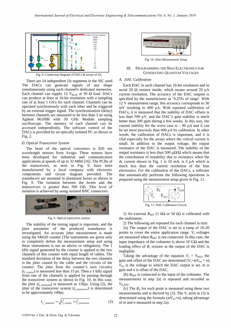
Fig. 8. Connection diagram of DACs & arrays of JJs.
There are 14 independent JJs segments in the SIC used. The DACs can generate signals of any shape simultaneously using each channel's dedicated memories. Each channel can supply 12 Vpk-pk at 50 Ω load. DACs can produce at least at 16-bit resolution with a sampling rate of at least 1 GS/s for each channel. Channels can be operated synchronously with each other and be triggered by an external trigger signal. The synchronization (delay) between channels are measured to be less than 3 ns using Agilent 86100B with 50 GHz Module sampling oscilloscope. The memory of each channel can be accessed independently. The software control of the DACs is provided by an optically isolated PC as shown in Fig. 2.
D. Optical Transceiver System
The heart of the optical converters is 820 nm wavelength sensors from Avago. These sensors have been developed for industrial and communication applications at speeds of up to 32 MBd [16]. The PCBs of the transceivers, as seen in Fig. 9, have been manufactured by a local company with electronic components and circuit diagram provided. The transducers are mounted in aluminum boxes as shown in Fig. 9. The isolation between the boxes and the transceivers is greater than 500 GΩ. This level of isolation is achieved by using isolated BNC connectors.
Fig. 9. Optical transceiver system.
The stability of the timing signal is important, and the jitter parameter of the produced transducers is investigated. An accurate jitter measurement is made using the SR620 counter (The instruments are given only to completely define the measurement setup and using these instruments is not an advice or obligation). The 1 kHz signal generated by the counter is applied to the two channels of this counter with equal length of cables. The standard deviation of the delay between the two channels is the jitter caused by the cable and the circuits of the counter. The jitter from the counter’s own circuitry (tj_counter) is measured less than 15 ps. Then a 1 kHz signal from one of the channels is applied by passing through the transceiver system as shown in Fig. 10. In this case, the jitter (tj_measured) is measured as 150ps. Using (2), the jitter of the transceiver system (tj_transceiver) is determined to be approximately 149ps.
2 2
_ measured _counter _transceiverj j jt t t (2)
Fig. 10. Jitter Measurement Setup.
III. PROGRAMMING THE BIAS ELECTRONICS FOR
GENERATING QUANTUM VOLTAGES
A. DAC Calibration
Each DAC in each channel has 16-bit resolution and in
serial 50 Ω resistor inside, which means around 20 μA
current resolution. The accuracy of the DAC outputs is
specified by the manufacturer as ‘0.25% of range'. With
12 V measurement range, this accuracy corresponds to 30
mV resulting to 600 μA. With repeated calibration of
DACs, it is measured that the stability of DAC offsets is
less than 500 μV, and the DAC’s gain stability is much
better than 300 ppm during a few weeks. In this way, the
current stability for the worst case is ~ 80 μA and it can
be set more precisely than 600 μA by calibration. In other
words, the calibration of DACs is important, and it is
vital especially for the arrays where the critical current is
small. In addition to the output voltage, the output
resistance of the DAC is measured. The stability of the
output resistance is less than 500 µΩ/Ω which means that
the contribution of instability due to resistance when the
dc current shown in Fig. 1 is 10 mA, is 5 µA which is
much less than the current resolution of the bias
electronics. For the calibration of the DACs, a software
that automatically performs the following operations is
prepared using the measurement setup given in Fig. 11.
Fig. 11. DAC Calibration Circuit.
1) An external RREF (1 kΩ or 50 Ω) is calibrated with
the multimeter,
2) The following are repeated for each channel in turn:
2a) The output of the DAC is set to a ramp of 10-20
points to cover the entire application range. Vx voltages
are measured when RREF is not connected. In this case, the
input impedance of the voltmeter is above 10 GΩ and the
loading effect of Rx resistor at the output of the DAC is
negligible.
Taking the advantage of the equation Vx = VREF, the
gain and offset of the DAC are determined (Vx=mVset + n).
Vset is the voltage to which the DAC output is set. m is
gain and n is offset of the DAC.
2b) RREF is connected to the input of the voltmeter. The
measurements in step 2a) is repeated and recorded as
VR_REF.
2c) The RX for each point is measured using these two
measurements and is derived by (3). The Vx term in (3) is
determined using the formula (mVset+n), taking advantage
of m and n measured in step 2a).
×
×
×
×
.
.
. ×
×
×
×
×
.
.
×
×
×
×
×
×
×
×
×
×
×
… V
n
Vn-1
In
In-1 I
1
V1
R1 Rn Rn-1
In_ideal
In-1_ideal
I1_ideal
Vn_JJ
Vn-1_JJ
V1_JJ
Number of JJs per segment
[4096
2048
1024
512
256
128
1
1
2
4
8
16
32
64]
I1_ideal
International Journal of Electrical and Electronic Engineering & Telecommunications Vol. 8, No. 1, January 2019
22©2019 Int. J. Elec. & Elecn. Eng. & Telcomm.
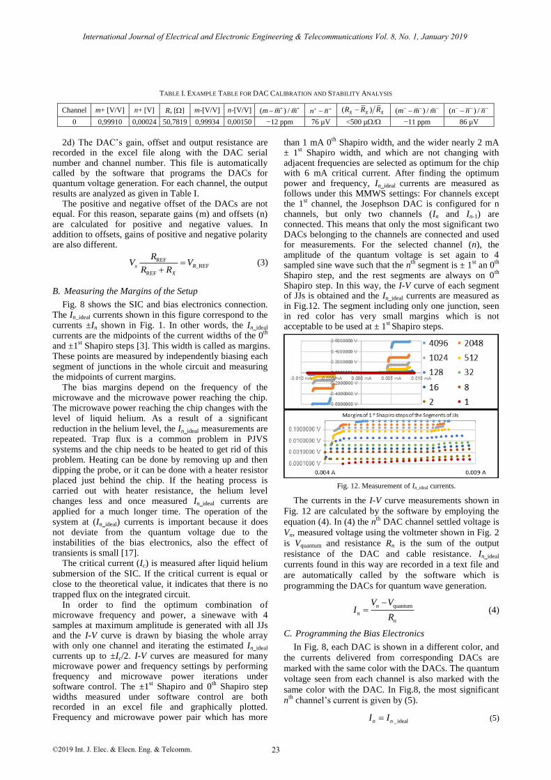
TABLE I. EXAMPLE TABLE FOR DAC CALIBRATION AND STABILITY ANALYSIS
Channel m+ [V/V] n+ [V] Rx [] m-[V/V] n-[V/V] ( ) /m m m n n ( )X X XR R R ( ) /m m m ( ) /n n n
0 0,99910 0,00024 50,7819 0,99934 0,00150 −12 ppm 76 µV <500 µ/ −11 ppm 86 µV
2d) The DAC’s gain, offset and output resistance are
recorded in the excel file along with the DAC serial number and channel number. This file is automatically called by the software that programs the DACs for quantum voltage generation. For each channel, the output results are analyzed as given in Table I.
The positive and negative offset of the DACs are not equal. For this reason, separate gains (m) and offsets (n) are calculated for positive and negative values. In addition to offsets, gains of positive and negative polarity are also different.
REF_REF
REF
x R
X
RV V
R R
(3)
B. Measuring the Margins of the Setup
Fig. 8 shows the SIC and bias electronics connection. The In_ideal currents shown in this figure correspond to the currents ±In shown in Fig. 1. In other words, the In_ideal
currents are the midpoints of the current widths of the 0th
and ±1
st Shapiro steps [3]. This width is called as margins.
These points are measured by independently biasing each segment of junctions in the whole circuit and measuring the midpoints of current margins.
The bias margins depend on the frequency of the microwave and the microwave power reaching the chip. The microwave power reaching the chip changes with the level of liquid helium. As a result of a significant reduction in the helium level, the In_ideal measurements are repeated. Trap flux is a common problem in PJVS systems and the chip needs to be heated to get rid of this problem. Heating can be done by removing up and then dipping the probe, or it can be done with a heater resistor placed just behind the chip. If the heating process is carried out with heater resistance, the helium level changes less and once measured In_ideal currents are applied for a much longer time. The operation of the system at (In_ideal) currents is important because it does not deviate from the quantum voltage due to the instabilities of the bias electronics, also the effect of transients is small [17].
The critical current (Ic) is measured after liquid helium submersion of the SIC. If the critical current is equal or close to the theoretical value, it indicates that there is no trapped flux on the integrated circuit.
In order to find the optimum combination of microwave frequency and power, a sinewave with 4 samples at maximum amplitude is generated with all JJs and the I-V curve is drawn by biasing the whole array with only one channel and iterating the estimated In_ideal
currents up to ±Ic/2. I-V curves are measured for many microwave power and frequency settings by performing frequency and microwave power iterations under software control. The ±1
st Shapiro and 0
th Shapiro step
widths measured under software control are both recorded in an excel file and graphically plotted. Frequency and microwave power pair which has more
than 1 mA 0th
Shapiro width, and the wider nearly 2 mA ± 1
st Shapiro width, and which are not changing with
adjacent frequencies are selected as optimum for the chip with 6 mA critical current. After finding the optimum power and frequency, In_ideal currents are measured as follows under this MMWS settings: For channels except the 1
st channel, the Josephson DAC is configured for n
channels, but only two channels (In and In-1) are connected. This means that only the most significant two DACs belonging to the channels are connected and used for measurements. For the selected channel (n), the amplitude of the quantum voltage is set again to 4 sampled sine wave such that the n
th segment is ± 1
st an 0
th
Shapiro step, and the rest segments are always on 0th
Shapiro step. In this way, the I-V curve of each segment of JJs is obtained and the In_ideal currents are measured as in Fig.12. The segment including only one junction, seen in red color has very small margins which is not acceptable to be used at ± 1
st Shapiro steps.
Fig. 12. Measurement of In_ideal currents.
The currents in the I-V curve measurements shown in
Fig. 12 are calculated by the software by employing the
equation (4). In (4) the nth
DAC channel settled voltage is
Vn, measured voltage using the voltmeter shown in Fig. 2
is
Vquantum and resistance Rn is the sum of the output
resistance of the DAC and cable resistance. In_ideal
currents found in this way are recorded in a text file and
are automatically called by the software which is
programming the DACs for quantum wave generation.
quantumn
n
n
V VI
R
(4)
C. Programming the Bias Electronics
In Fig. 8, each DAC is shown in a different color, and
the currents delivered from corresponding DACs are
marked with the same color with the DACs. The quantum
voltage seen from each channel is also marked with the
same color with the DAC. In Fig.8, the most significant
nth
channel’s current is given by (5).
_ idealn nI I (5)
International Journal of Electrical and Electronic Engineering & Telecommunications Vol. 8, No. 1, January 2019
23©2019 Int. J. Elec. & Elecn. Eng. & Telcomm.
1_ ideal _ ideal 1 1 1_ ideal _ ideal; n n n n n nI I I I I I (6)
By using (6), each DAC’s current is calculated. For
example, if each JJs is programmed in the +1st Shapiro
and If In_ideal = 7 mA and In-1_ideal = 7.2 mA are measured,
then In-1 should be In-1 = 0.2 mA. After calculating each
DACs current, each DAC voltage is calculated using the
(7). Vn_JJ in (7) is the Josephson Voltage seen from the nth
DAC. Satisfying (7) guaranties DAC currents to flow as
shown in Fig. 8.
_ JJn n n nV I R V (7)
With the first 4 AWG generators, 14 independent
DACs are used to bias the 14 independent segments as
shown in Fig. 8 to the appropriate Shapiro step. The
trigger signal per period is generated from 15th
channel.
In the 16th
channel, a trigger signal per measurement is
generated. To generate arbitrary quantized waves, DACs
are programmed as follows:
1) Arbitrary wave parameters to be generated: wave
shape, amplitude, step number are selected via the
interface program.
2) Each step is quantized by the quantization algorithm.
3) For each quantum step, the voltages of the 14 DACs
are calculated using (5) - (7). The voltages of each DAC
are stored in arrays and are recorded in files with the
channel’s name.
4) This process is repeated for each quantum step in
sequence.
5) Recorded voltages are corrected using the generated
calibration file recorded as in Table I. Corrected DAC
voltages are recorded to each independent DAC's
memory of the generators as a 4-step DC wave.
At each external trigger pulse, the DAC voltages are
triggered to the next quantum voltage. The trigger signal
is generated by an additional 5th
AWG generator. The
frequency of the trigger signal is equal to the frequency
of the signal multiplied by the number of steps. In
addition, timing signals are produced at frequencies of 20
MHz and 10 MHz from the 5th
generator.
Fig. 13. Static linearity measurement results.
IV. METROLOGICAL MEASUREMENTS
A. Static ADC Characterization
Whether the voltage output is at quantum level for all
codes/steps can be controlled quickly by using the
voltmeter in the system. The ADC is also statically
characterized by evaluating the results of this control. Fig.
13 is a result of this static calibration. The measured
stability of the gain is much less than 0.5 ppm which is
previously declared in [18] and it is obvious that the gain
of the ADC is independent from Isegtrim that indicates the
quantum state.
B. Solid State Voltage Standard (SSVS) Calibration
SSVSs are traceable to the Conventional JVSs. Rather
than directly comparing the JVSs, to use the SSVS as a
transfer standard has been preferred in terms of the
simplicity and the cost of measurement. Established
PJVS system is compared with the SSVS. Measurement
results are summarized in Fig.14. Measurement results
show that the result is independent from Isegtrim and the
two results are agreed within the stability of SSVS.
Fig. 14. History and measurement results of the SSVS
C. Dynamic ADC Characterization
Dynamic ADC Characterization is explained in more
detail in [18], the PJVS standard is used to investigate
how ADC gain changes depending on the dynamic
conditions. For this measurement, the ADC is modified to
take out its timing signal using developed optical
transceiver system. This timing signal is applied to the
bias electronics as seen in Fig. 2, which is important to
obtain measurements at the center of the quantum steps.
In Fig. 15, the obtained measurement results are
summarized.
Fig. 15. Dynamic ADC characterization.
V. CONCLUSIONS
In this article, Programmable Josephson Voltage
Standard system established in UME was presented.
Every part of the system was bought/manufactured
separately and tested according to the needs of the system.
The necessary measurements of microwave, cryoprop,
optical transceivers and bias electronics to maintain the
quantum accuracy of the output voltage are given in
detail. The hints of the software for generating quantum
voltages and easy use of the system were described. The
system was used in static and dynamic ADC
characterization and SSVS calibration. Measurement
results has shown that the system was established
International Journal of Electrical and Electronic Engineering & Telecommunications Vol. 8, No. 1, January 2019
24©2019 Int. J. Elec. & Elecn. Eng. & Telcomm.
International Journal of Electrical and Electronic Engineering & Telecommunications Vol. 8, No. 1, January 2019
25©2019 Int. J. Elec. & Elecn. Eng. & Telcomm.
successfully. A detailed procedure about the
measurements and uncertainty evaluation were presented
in [19].
ACKNOWLEDGEMENT
This work is partly carried out with funding by the
European Union within the EMRP Q-WAVE and EMPIR
QuADC projects. The EMPIR initiative is so co-funded
by the European Union’s Horizon 2020 research and
innovation program and the EMPIR Participating States.
T.C.Ö. wants to thank Ralf Behr and Johannes Kohlmann
for valuable discussions on Josephson Voltage Standard
Systems and PTB for borrowing the SIC. T.C.Ö. also
wants to thank to Menar Electronics for their cooperation
in PCB manufacturing of the optical transceivers and
Gülmak Tor.Tes.San.Pls.İml.Ltd.Şti. for waveguide
converters (horn antennas) manufacturing. T.C.Ö. also
wants to thank to Saliha Turhan for her support on
waveguide manufacturing and Mehedin Arifoviç for his
resource leading within the laboratory.
REFERENCES
[1] B. D. Josephson, “Possible new effects in superconductive
tunneling,” Phys. Letters, vol. 1, no. 7, pp. 251-253, 1962.
[2] P. Anderson and J. M. Rowell, “Probable observation of the
Josephson superconducting effect,” Phys. Rev. Lett., vol. 10, no. 6,
pp. 230-232, 1963.
[3] S. Shapiro, “Josephson currents in superconducting tunneling: The
effect of microwaves and other observations,” Phys. Letters, vol.
11, no. 2, pp. 80-82, July, 1963.
[4] P Pöpel and R., “The Josephson effect and voltage standards,”
Metrologia, vol. 29, no. 2, pp. 153-174, 1992.
[5] V. Sienknecht and T. Funck, “Realization of the SI unit volt by
means of a voltage balance,” Metrologia, vol. 22, no. 3, pp. 209-
212, 1986.
[6] B. N. Taylor and T. J. Witt, “New international electrical reference
standards based on the Josephson and quantum hall effects,” Metrologia, vol. 26, no. 1, pp. 47-62, 1989
[7] S. P. Benz and C. A. Hamilton, “Application of the Josephson effect to voltage metrology,” Proc. of the IEEE, vol. 92, no. 10, pp.
1617-1629, 2004.
[8] R. L. Kautz, “On a proposed Josephson effect voltage standard at zero current bias,” Appl. Phys. Lett., vol. 36, no. 5, pp. 386-388,
1980.
[9] R. Behr, O. Kieler, J. Kohlmann, F. Müller, and L. Palafox, “Development and metrological applications of Josephson arrays
at PTB,” Meas. Sci. Technol., vol. 23, no. 12, 2012.
[10] J. Lee, R. Behr, B. Schumacher, L. Palafox, M. Starkloff, A. C.
Böck, and P. M. Fleischmann, “From AC quantum voltmeter to
quantum calibrator,” presented at Conf. on Precision Electromagnetic Measurements, Ottawa Canada, 10-15 July, 2016.
[11] F. Mueller, R. Behr, T. Weimann, L. Palafox, D. Olaya, P. D.
Dresselhaus, and S. P. Benz, “1 V and 10 V SNS programmable voltage standards for 70 GHz,” IEEE Trans. Appl. Supercond., vol.
19, no. 3, pp. 981-986, Jun. 2009.
[12] EMPIR (2015). QuADC: Waveform metrology based on
spectrally pure Josephson voltages. [Online]. Available:
https://www.ptb.de/empir/quadc-project.html
[13] İ. Ünal, M. Tekbaş, A. Kaya, T. Coşkun Öztürk, “Millimeter wave
synthesizer for Josephson voltage standard system,” presented at Elektrik Elektronik ve Biyomedikal Müh. Konferansı, Bursa,
Turkey, December 1-3, 2016.
[14] M. Schubert, M. Starkloff, J. Lee, R. Behr, L. Palafox, A. Wintermeier, A. C. Böeck, P. M. Fleischmann, and T. May “An
AC Josephson voltage standard up to kilohertz range tested in a
calibration laboratory,” IEEE Trans. Instr. Meas., vol. 64, no. 6, pp. 1620-1626, 2015.
[15] J. M. Williams, D. Henderson, P. Patel, R. Behr, and L. Palafox, “Achieving sub-100-ns switching of programmable Josephson
arrays,” IEEE Trans. Instr. Meas., vol. 56, no. 2, pp. 651–654,
2007.
[16] A. Technologies. Inexpensive dc to 32 MBd fiberoptic solutions
for industrial, medical, telecom, and proprietary data
communication applications. [Online]. Available: ttps://media.
digikey.com/pdf/data%20sheets/avago%20pdfs/fiberoptic_solutio
ns_appnote.pdf
[17] J. Lee, R. Behr, A. S. Katkov, and L. Palafox, “Modeling and
measuring error contributions in stepwise synthesized Josephson
sine waves,” IEEE Trans. Inst. Meas., vol. 58, no. 4, pp. 803–808, 2009.
[18] K. W. G. Ihlenfeld, Maintenance and Traceability of AC Voltages by Synchronous Digital Synthesis and Sampling, Braunschweig,
Germany: PTB Report E-75, 2001.
[19] T. C. Öztürk, S. Ertürk, A. Tangel, S. Turhan, and M. Arifoviç, “Metrological measurements using programmable Josephson
voltage standard,” presented at 10th Int. Conf. on Electrical and
Electronics Engineering, Bursa, Turkey, November 30- December 2, 2017.