Embed Size (px)
Citation preview

ES10: Intro to Material Science
Andrew Rosen
April 23, 2013
Contents
1 Introduction 3
1.1 Types of Materials . . . . . . . . . . . . . . . . . . . . . . . . . . . . . . . . . . . . . . . . . . . . . . . . . . . 3
1.2 Processes and Properties . . . . . . . . . . . . . . . . . . . . . . . . . . . . . . . . . . . . . . . . . . . . . . . . 3
2 Atomic Structure and Interatomic Bonding 3
2.1 Basics of the Periodic Table . . . . . . . . . . . . . . . . . . . . . . . . . . . . . . . . . . . . . . . . . . . . . . 3
2.2 Electrons in Atoms . . . . . . . . . . . . . . . . . . . . . . . . . . . . . . . . . . . . . . . . . . . . . . . . . . . 3
2.3 Bonding Forces and Energies . . . . . . . . . . . . . . . . . . . . . . . . . . . . . . . . . . . . . . . . . . . . . 4
2.4 Bonding . . . . . . . . . . . . . . . . . . . . . . . . . . . . . . . . . . . . . . . . . . . . . . . . . . . . . . . . . 4
3 Structures of Metals and Ceramics 4
3.1 Metallic Crystal Structures . . . . . . . . . . . . . . . . . . . . . . . . . . . . . . . . . . . . . . . . . . . . . . 4
3.1.1 Properties . . . . . . . . . . . . . . . . . . . . . . . . . . . . . . . . . . . . . . . . . . . . . . . . . . . . 4
3.1.2 Terminology . . . . . . . . . . . . . . . . . . . . . . . . . . . . . . . . . . . . . . . . . . . . . . . . . . 5
3.1.3 Atomic Packing Factor . . . . . . . . . . . . . . . . . . . . . . . . . . . . . . . . . . . . . . . . . . . . . 5
3.1.4 Simple Cubic (SC) Structure . . . . . . . . . . . . . . . . . . . . . . . . . . . . . . . . . . . . . . . . . 5
3.1.5 The Body-Centered Cubic (BCC) Crystal Structure . . . . . . . . . . . . . . . . . . . . . . . . . . . . 5
3.1.6 The Face-Centered Cubic (FCC) Crystal Structure . . . . . . . . . . . . . . . . . . . . . . . . . . . . . 6
3.1.7 The Hexagonal Close-Packed (HCP) Crystal Structure . . . . . . . . . . . . . . . . . . . . . . . . . . . 6
3.2 Density Computations - Metals . . . . . . . . . . . . . . . . . . . . . . . . . . . . . . . . . . . . . . . . . . . . 6
3.3 Ceramic Crystal Structure and Density . . . . . . . . . . . . . . . . . . . . . . . . . . . . . . . . . . . . . . . . 7
3.4 Carbon, Polymorphism, and Allotropy . . . . . . . . . . . . . . . . . . . . . . . . . . . . . . . . . . . . . . . . 7
3.5 Crystallographic Points, Directions, and Planes . . . . . . . . . . . . . . . . . . . . . . . . . . . . . . . . . . . 7
3.5.1 Miller Indices for Points and Vectors . . . . . . . . . . . . . . . . . . . . . . . . . . . . . . . . . . . . . 7
3.5.2 Miller Indices for Planes . . . . . . . . . . . . . . . . . . . . . . . . . . . . . . . . . . . . . . . . . . . 7
3.6 Linear and Planar Densities . . . . . . . . . . . . . . . . . . . . . . . . . . . . . . . . . . . . . . . . . . . . . . 8
3.7 X-Ray Di�raction: Determination of Crystal Structures . . . . . . . . . . . . . . . . . . . . . . . . . . . . . . 8
4 Polymer Structures 8
4.1 Degree of Polymerization . . . . . . . . . . . . . . . . . . . . . . . . . . . . . . . . . . . . . . . . . . . . . . . 8
4.2 Molecular Structure . . . . . . . . . . . . . . . . . . . . . . . . . . . . . . . . . . . . . . . . . . . . . . . . . . 9
4.3 Tacticity . . . . . . . . . . . . . . . . . . . . . . . . . . . . . . . . . . . . . . . . . . . . . . . . . . . . . . . . 9
4.4 Thermal Behavior . . . . . . . . . . . . . . . . . . . . . . . . . . . . . . . . . . . . . . . . . . . . . . . . . . . 9
4.4.1 Thermoplastics - Think of Plastic . . . . . . . . . . . . . . . . . . . . . . . . . . . . . . . . . . . . . . . 9
4.4.2 Thermosetting - Think of Proteins . . . . . . . . . . . . . . . . . . . . . . . . . . . . . . . . . . . . . . 9
4.5 Copolymers . . . . . . . . . . . . . . . . . . . . . . . . . . . . . . . . . . . . . . . . . . . . . . . . . . . . . . . 9
4.6 Crystallinity . . . . . . . . . . . . . . . . . . . . . . . . . . . . . . . . . . . . . . . . . . . . . . . . . . . . . . . 10
1
5 Imperfections in Solids 10
5.1 Introduction . . . . . . . . . . . . . . . . . . . . . . . . . . . . . . . . . . . . . . . . . . . . . . . . . . . . . . . 10
5.2 Point Defects in Metals . . . . . . . . . . . . . . . . . . . . . . . . . . . . . . . . . . . . . . . . . . . . . . . . 10
5.3 Composition . . . . . . . . . . . . . . . . . . . . . . . . . . . . . . . . . . . . . . . . . . . . . . . . . . . . . . . 11
5.4 Point Defects in Ceramics . . . . . . . . . . . . . . . . . . . . . . . . . . . . . . . . . . . . . . . . . . . . . . . 11
5.5 Interfacial Defects . . . . . . . . . . . . . . . . . . . . . . . . . . . . . . . . . . . . . . . . . . . . . . . . . . . 12
5.6 Miscellaneous Imperfections . . . . . . . . . . . . . . . . . . . . . . . . . . . . . . . . . . . . . . . . . . . . . . 12
6 Di�usion 12
6.1 Introduction . . . . . . . . . . . . . . . . . . . . . . . . . . . . . . . . . . . . . . . . . . . . . . . . . . . . . . . 12
6.2 Steady-State Di�usion . . . . . . . . . . . . . . . . . . . . . . . . . . . . . . . . . . . . . . . . . . . . . . . . . 13
6.3 Nonsteady-State Di�usion . . . . . . . . . . . . . . . . . . . . . . . . . . . . . . . . . . . . . . . . . . . . . . . 13
7 Mechanical Properties 13
7.1 Concepts of Stress and Strain . . . . . . . . . . . . . . . . . . . . . . . . . . . . . . . . . . . . . . . . . . . . . 13
7.2 Stress-Strain Behavior and Elastic Properties of Materials . . . . . . . . . . . . . . . . . . . . . . . . . . . . . 14
7.3 Mechanical Behavior Models . . . . . . . . . . . . . . . . . . . . . . . . . . . . . . . . . . . . . . . . . . . . . 14
7.4 True Stress and Strain . . . . . . . . . . . . . . . . . . . . . . . . . . . . . . . . . . . . . . . . . . . . . . . . . 14
8 Deformation and Strengthening Mechanisms 14
8.1 Dislocations . . . . . . . . . . . . . . . . . . . . . . . . . . . . . . . . . . . . . . . . . . . . . . . . . . . . . . . 14
8.2 Mechanisms of Strengthening in Metals . . . . . . . . . . . . . . . . . . . . . . . . . . . . . . . . . . . . . . . 15
9 Phase Diagrams 15
9.1 De�nitions . . . . . . . . . . . . . . . . . . . . . . . . . . . . . . . . . . . . . . . . . . . . . . . . . . . . . . . . 15
9.2 Binary Isomorphous System . . . . . . . . . . . . . . . . . . . . . . . . . . . . . . . . . . . . . . . . . . . . . . 16
9.3 Binary Eutectic Systems . . . . . . . . . . . . . . . . . . . . . . . . . . . . . . . . . . . . . . . . . . . . . . . . 16
10 Thermal Properties 16
10.1 Mathematics . . . . . . . . . . . . . . . . . . . . . . . . . . . . . . . . . . . . . . . . . . . . . . . . . . . . . . 16
10.2 Trends . . . . . . . . . . . . . . . . . . . . . . . . . . . . . . . . . . . . . . . . . . . . . . . . . . . . . . . . . . 17
11 Electrical Properties 17
12 Optical Properties 18
2

1 Introduction
1.1 Types of Materials
� Metals are strong, ductile, have high thermal/electrical conductivity, are opaque, and are re�ective
� Polymers/plastics have secondary bonding, are soft, ductile, low strength, have low density, are thermal/electricalinsulators, and are optically translucent or transparent
� Ceramics have mostly ionic bonding. They are brittle, glassy, elastic, and insulators
� Semiconductors have covalent bonding and have electrical properties that are between conductors and insulators
� A composite consists of more than one material type
� Biomaterials have covalent and hydrogen bonding, ionic interactions, and hydrophobic interactions. They are �exible,hydrophilic, programmable, �smart,� and selective
� Nanomaterials have properties governed by size and also have high surface-to-volume ratios
1.2 Processes and Properties
� Adding �impurity� atoms to a metal, such as copper, can increase electrical resistivity
• Deformation can also cause increases resistivity
� Optical transmittance is dependent on material structure, such as single crystal vs. polycrystal and degree of porosity
• A single crystal of aluminum oxide will be transparent, a polycrystal with no porosity will be translucent, and apolycrystal with some porosity will be opaque
� Stress and saltwater can cause deteriorative cracks
• Heat treatment slows crack speed in salt water
2 Atomic Structure and Interatomic Bonding
2.1 Basics of the Periodic Table
� The mass number of an atom is always a whole number (protons and neutrons)
� The atomic weight is a weighted average of the mass numbers of the isotopes of the given element
2.2 Electrons in Atoms
� The principal quantum number, n, de�nes the energy of an orbital and average distance of an electron from the nucleus
• Orbitals with the same n value form a shell
• n ≥ 1
∗ Sometimes shells are designated with letters where n = 1 = K, n = 2 = L, etc.
� The subsidary number, l, signi�es the subshell and its shape
• l = 0 to n− 1
∗ The s orbital corresponds to l = 0, the p orbital for l = 1, the d orbital for l = 2, the f orbital for l = 3, etc.
� The magnetic quantum number, ml, describes the number of energy states for the orbital
• −l ≤ ml ≤ l
� The spin quantum number, ms, describes the spin moment of the electrons
• ms = +1
2or −1
2
3

2.3 Bonding Forces and Energies
� The bonding energy is the energy that is required to separate two atoms to an in�nite separation
� To calculate the attractive Coulombic force between charges1 where Z1 and Z2 are the valences of the ions,
FA =1
4πε0
q1q2r2
= k0e2Z1Z2
r2
• Note that e = 1.602× 10⁻¹⁹C
� To calculate the repulsive force2,
FR =−bn
rn+1
� Energy and force are related as,
Enet =
ˆFA dr +
ˆFR dr = −A
r+B
rn
• Here, A = k0e2Z1Z2 and B is found via an empirical plot
� In a plot of energy versus distance, the minimum is known as the equilibrium distance
• The magnitude of energy is the bonding energy
• Dense, ordered molecules with higher melting point in temperature have higher bonding energies and lower po-tential energies; therefore, they are more stable
2.4 Bonding
� The percent ionic character of a bond between elements A and B is the following where X refers to the electronegativityof an element3,
%IC =(
1− exp[−(0.25) (XA −XB)
2])· 100%
� Metallic bonding and ionic bonding is non-directional while covalent bonding and secondary bonding are directional
� In order of increasing intermolecular force strength: �uctuating induced dipole < polar molecule induced dipole <hydrogen bonding (permanent dipole moment)
3 Structures of Metals and Ceramics
3.1 Metallic Crystal Structures
3.1.1 Properties
� Densely packed due to:
• Only one element is present, so all atomic radii are identical
• Metallic bonding is not directional
• Nearest neighbor distances are small and thus lower bonding energy
• Electron cloud shields cores from one another
� Metals have the simplest crystal structures
1k0 = 8.99 × 10⁹ Nm2/C2
2n ≈ 9 for ionic constant3This formula does not need to be memorized
4
3.1.2 Terminology
� A crystalline material has atoms arranged in a periodic array over large atomic distances
• All metals, many ceramics, and some polymers are crystalline
� Noncrystalline �amorphous� materials have no periodic packing
• This occurs for complex structures and under rapid cooling conditions
� Unit cells are small repeating entities of a crystalline material
3.1.3 Atomic Packing Factor
� The atomic packing factor is the following:
APF=Volume of atoms in a unit cell
Total unit cell volume=N ·
43πR
3
a3=VSVC
3.1.4 Simple Cubic (SC) Structure
� There are N = 1 atoms in an SC unit cell with R = 0.5a and coordination number of 6
APF =1 · 4
3π (0.5a)
3
a3=
4
3π · 0.53 ≈ 0.52
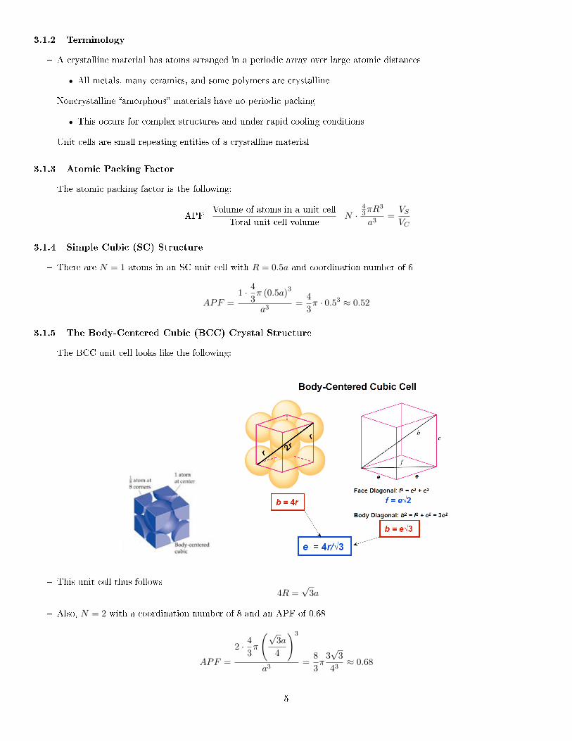
3.1.5 The Body-Centered Cubic (BCC) Crystal Structure
� The BCC unit cell looks like the following:
� This unit cell thus follows4R =
√3a
� Also, N = 2 with a coordination number of 8 and an APF of 0.68
APF =
2 · 4
3π
(√3a
4
)3
a3=
8
3π
3√
3
43≈ 0.68
5

3.1.6 The Face-Centered Cubic (FCC) Crystal Structure
� The FCC unit cell is cubic with atoms located at each of the corners and the centers of all faces
� The cube length, a, and atomic radius, R, are related by,
4R =√
2a
• This is true because the diagonal of the unit cell face is 4R, and since it's an isosceles triangle, the ratio isa : a :
√2a
� N = 4 for FCC crystals (six face atoms and eight corner atoms) and has a coordination number of 12
APF =
4 · 4
3π
(√2a
4
)3
a3=
16
3π
2√
2
43≈ 0.74
3.1.7 The Hexagonal Close-Packed (HCP) Crystal Structure
� HCP crystal is not cubic:
� For HCP, N = 6 with a coordination number of 12 and an APF of 0.74 just like FCC where 2R = a
VHCP = 6R2c√
3 =3√
3
2a2c
3.2 Density Computations - Metals
� Metals are dense because they have close packing due to metallic bonding and large atomic masses
� Ceramics have less dense packing since they are lighter and are made of covalent bonding
� Polymers have poor packing and use even lighter hydrocarbon elements
� Composites have intermediate densities
� The theoretical density of a metallic solid, ρ, is given by the following equation where n is the number of atomsassociated with each unit cell, M is the atomic weight, VC is the volume of the cell, and NA is Avogadro's Constant:
ρ =nM
VCNA
� Since VC usually equals a3,
ρ =nM
a3NA
6

3.3 Ceramic Crystal Structure and Density
� For ceramics with ionic character, the magnitude of the electrical charge on each component ion and the relative sizeof the ions play a role in determining the structure
• The charge indicates the ratio of ions since the crystal must be neutral
• The number of oppositely charged ion neighbors is maximized
� Coordination number increases withrcationranion
� The density can be calculated as follows where the new variables are n′ (number of formula units within the unit cell),AC (atomic weights of cations in formula unit), AA (atomic weights of anions in formula unit):
ρ =n′ (∑AC +
∑AA)
VCNA
� In oxide structures, oxygen anions are larger than metal cations, the oxygen anions are closely packed (typically FCC),and cations �t into interstitial sites among the oxygen anions
3.4 Carbon, Polymorphism, and Allotropy
� The group IVA elements form structures known as diamond cubic crystals (e.g. carbon diamond)
� Graphite is more stable than diamond and is composed of layered hexagonal carbons
� Polymorphism is when a metal or nonmetal may have more than one crystal structure
• This is called allotropy for elemental solids
3.5 Crystallographic Points, Directions, and Planes
3.5.1 Miller Indices for Points and Vectors
� Crystallographic directions are vectors that pass through the origin. The length of the projection on each axis ismeasured in terms of the unit cell dimensions a, b, and c. The three values are scaled to create the smallest integervalues. Then, the three indices are enclosed in a square bracket without commas - [uvw]
• A negative index will have a bar over the value
• Families of directions are expressed in angled brackets, < >
∗ There is the same packing density along a family of directions
∗ To �nd di�erent components of the family, one can switch the order of the three numbers and/or the sign
� In simpler terms, to �nd the indices for a direction (vector), �nd ∆x, ∆y, and ∆z, and then scale them to the nearestinteger
3.5.2 Miller Indices for Planes
1. If the plane passes through the origin, create a new origin
2. Read the intercepts of the plane with axes in terms of x, y, and z
(a) If it always intercepts, the value is ∞ (reciprocal is 0)
(b) A plane that parallels an axis may be considered to have ∞ intercept, too
3. Take the reciprocals of the intercepts
4. Reduce to smallest integer values
5. Enclose in parentheses without commas
(a) Families of planes are written with squiggly brackets, { }
i. There is the same packing density along a family of planes
(b) To describe a plane and a vector, use the format of [a b c] ⊥ (h j k)
7
3.6 Linear and Planar Densities
� Linear density is given by,
LD =length of atoms centered on direction vector
length of direction vector× 100%
• For instance, for BCC along [1 0 0], LD =2R
a=
a√
3
2a
=
√3
2≈ 86.6%
� The planar density is given by,
PD =area of atoms centered on a plane
area of plane× 100%
• For instance, for FCC along (1 1 0), the plane goes through 1 whole and 4-quarters of atoms. Therefore4, PD =
2(πR2
)a · a√
2=
2π
(a√
2
4
)2
a2√
2≈ 55.5%
3.7 X-Ray Di�raction: Determination of Crystal Structures
� The condition for di�raction (Bragg's Law) is,nλ = 2dhkl sin θ
• n is the order of re�ection (an integer)
� The di�raction angle is given as,Di�raction Angle = 2θ
� The magnitude of the distance between two adjacent and parallel planes of atoms for a cubic symmetry crystal is,
dhkl =a√
h2 + k2 + l2
� To get a peak from FCC, the miller indices must be all odd or all even
� To get a peak from BCC, h+ k + l must be even
� Larger miller indices indicate shorter distances between planes for the same a value, so then it corresponds bigger angle
4 Polymer Structures
4.1 Degree of Polymerization
� Polymers are made up of long chains of molecules of repeating chemical structure
� The amount of repeating units, n, is known as the degree of polymerization (does not have to be an integer)
n =Molar weight of polymer
Molar weight of substituent
� Polymorphism is when two or more crystal structures are possible for a material of given composition
� The three steps of addition polymerization are initiation, propagation, and termination
� The molecular weight of polymers is an average can be found via two methods
• Number-average: M̄n =∑xiMi (where xi is the fraction of the total number of chains within the corresponding
size range)
• Weight-average: M̄w =∑wiMi (where wi is the weight fraction of molecules within the same size range)
• The value of Mi is the mean molecular weight within the size range
4The area of the plane is simply base times height
8
4.2 Molecular Structure
� Linear polymers have repeat units joined together end to end in a single chain
� Branched polymers have side-branch chains connected to the main ones
� Crosslinked polymers have adjacent linear chains that are joined to one another at various positions by covalent bonds
� Network polymers are three-dimensional networks of multifunctional monomers
4.3 Tacticity
� Isotactic polymers have all the substituents located on the same side of the macromolecular backbone
� Syndiotactic polymers have alternating positions (up/down) along the chain
� Atactic polymers have substituents placed randomly along the chain
4.4 Thermal Behavior
4.4.1 Thermoplastics - Think of Plastic
� Soften when heated and harden when cooled
� Easily reshape and are recyclable due to presence of long chains that limits crosslinks
� Weak attractive forces between chains are broken by warming
� When cooled the weak forces reform the structure into a new shape
� Are linear and branched structured
4.4.2 Thermosetting - Think of Proteins
� Decompose when heated and thus cannot be reformed or recycled
� Extensive crosslinking due to covalent bonds induce decomposition upon heating and renders them brittle
� Bonds prevent chains moving relative to each other
� Are network polymers with cross-links
� Fast cooling yields a greater volume; slow cooling yields a smaller volume that is more rigid and dense
4.5 Copolymers
� Pure polymers are known as homopolymers
� Copolymers have di�erent repeating units
• PE−C−PVC would be a copolymer (note that the C stands for �copolymer� and is not a carbon atom)
� Copolymers come in di�erent types:
• Random copolymer: No pattern associated with copolymer (e.g. AABABBABAB)
• Alternating copolymer: Directly alternating sequence of units (e.g. ABABABABA)
∗ Therefore, alternating copolymers have chain fractions of 0.5 for each repeat unit type (assuming 2 repeattypes)
• Block copolymer: One block of identical repeating units followed by a block of the other unit (e.g. AAAABBB-BAAAA)
• Graft copolymer: Where homopolymer side branches of one type are grafted onto homopolymer main chains thatare composed of a di�erent repeating unit
9

4.6 Crystallinity
� Crystalline regions of polymers have chain folded structures
� Low density polymers have higher optical transparency while high density polymers are opaque
� Crystallized structures have higher indices of refraction than amorphous materials
� The degree of crystallinity can be given by the following equation where ρc is the density of a perfectly crystallinepolymer, ρa is the density of the totally amorphous polymer, and ρs is the density of the sample polymer
%Crystallinity =ρc (ρs − ρa)
ρs (ρc − ρa)× 100%
• Heat treating increases % crystallinity
• Recall that number of repeat units per unit cell is,
n =ρVCNAA
� Electrical insulators, mechanically light, opaque or transparent, chemically inert, and are solid at room temperature
� The tendency of a polymer to crystallize decreases with increasing molecular weight because longer chains make it moredi�cult to align adjacent chains in the correct atomic crystal array
5 Imperfections in Solids
5.1 Introduction
� Point defects are defects in one or two atomic positions
• A vacancy has an atom missing
• A self-interstitial site has an atom crowded in an interstitial site, which is a small void space that is unoccupiedunder normal conditions
• Interstitials don't usually exist for anions due to their large size
� Line defects occur when some atoms of a lattice are misaligned and produce permanent (plastic) deformation
� Planar defects occur where the crystallographic direction of the lattice abruptly changes
� Bulk defects have voids and/or impurities that cluster together to form small regions of a di�erent phase
� Solidi�cation is the result of casting molten material where nuclei form and then grow to form crystals
5.2 Point Defects in Metals
� To �nd the number of vacancies where N is the number of atomic sites and Qv is the energy required to form a vacancy,
NvN
= exp
(−QvkT
)
N =NAρ
A
� For Frenkel and Schottky defects (see 5.3), the above equation uses 2kT in the denominator of the exponential insteadof kT
10
5.3 Composition
� Weight percent is de�ned as,
C1 =m1
m1 +m2× 100%
� Atom percent is de�ned as,
C ′1 =nm1
nm1 + nm2× 100%
� Converting weight percent to atom percent,
C ′1 =C1A1
C1A2 + C2A1× 100%
� Converting from atom percent to weight percent,
C1 =C ′1A1
C ′1A1 + C ′2A2× 100%
� Converting weight percent to mass per unit volume,
C′′
1 =
C1
C1
ρ1+C2
ρ2
� Converting weight percent to density,
ρave =100
C1
ρ1+C2
ρ2
� Remember that for an alloy,
ρave =nAaveVCNA
� Converting weight percent to atomic weight,
Aave =100
C1
A1+C2
A2
� Converting weight percent to number of atoms per unit volume,
N1 =NAC1
C1A1
ρ1+C2A1
ρ2
� Converting weight percent to number of atoms per unit volume,
C1 =100
1 +NAρ2N1A1
− ρ2ρ1
5.4 Point Defects in Ceramics
� Schottky defects consist of cation-anion vacancies
• Each defect must be electroneutral. So, if we have K2O, each defect would have one O−2 and two K+ vacancies
� Frenkel defects consist of a cation vacancy and cation interstitial pairs
� There are two types of impurities:
• Substitutional impurities have impurity atoms substituting the host atoms
∗ Needs similar atomic size (within ±15%), same crystal structure, similar electronegativities, and higher va-lencies are favored
• Interstitial impurities have atoms �lling the voids or interstices among the host atoms
∗ Therefore, the impurity atoms must have small atomic radii
11
5.5 Interfacial Defects
� There is the external surface boundary, which is a higher-energy state than atoms at interior positions since the surfaceatoms are not bonded to the maximum number of neighbors
• This energy is termed �surface energy�, and it is stabilized by minimizing surface area
� A grain boundary separates two regions of a crystal that have di�erent crystallographic orientations
• The magnitude of the grain boundary energy is directly related to the angle of misorientation
• These areas are more chemically reactive due to higher energies
� A twin boundary is a re�ection of atom positions across a plane
5.6 Miscellaneous Imperfections
� Dislocation: a linear or 1D defect around which some of the atoms are misaligned. It's de�ned by a dislocation lineand Burger's vector
� Burgers vector (−→b ): The measure of lattice distortion
• The Burgers vector and dislocation line are perpendicular for edge dislocations, parallel for screw, and neitherparallel nor perpendicular for mixed
� Edge dislocation: an extra half-plane of atoms inserted into a crystal structure where−→b is ⊥ to the dislocation line
� Screw dislocation: a spiral planar ramp resulting from shear deformation where−→b is ‖ to the dislocation line
� Mixed dislocation: a combination of screw and edge dislocations
� Interfacial defects (2D):
• External surfaces: surface atoms are not bonded to the maximum number of nearest neighbors, in a higher-energystate than in the interior
∗ Materials minimize total surface area to minimize surface energy
• Grain boundary: the boundary separating two small grains or crystals having di�erent crystallographic orientationsin a polycrystalline material
∗ Grain boundary energy will always be less than the surface energy since grain boundaries have some atomsbonding across the boundary whereas the surface does not have this
� The ASTM grain size can be found via the following formula where n is grain sizes and N is the number of grains persquare inch at a magni�cation of 100x
N100 = 2n−1
� To convert NM to N100, use
N100 = NM
(Magni�cation
100
)2
6 Di�usion
6.1 Introduction
� Interdi�usion is when atoms tend to migrate from regions of high concentration to low concentration
� Self-di�usion is di�usion within an elemental solid where atoms migrate, but these atoms are all the same type
12
6.2 Steady-State Di�usion
� Rate of mass transfer uses the variable J to indicate the di�usion �ux where M is mass, A is area, and t is time,
J =M
At
� The concentration gradient is,dC
dx≈ ∆C
∆x=CB − CAXB −XA
� Fick's First Law states the following where D is the di�usion coe�cient and the derivative is the concentration gradient,
J = −DdCdx
D = D0 exp
(−QdRT
)
6.3 Nonsteady-State Di�usion
� Non-steady state di�usion is time-variant
� Fick's Second Law statesdC
dt= D
(d2C
dx2
)� The following assumptions can be made to simplify the solution set:
• Before di�usion, the di�using solute atoms are uniformly distributed
• The value of x at the surface is zero and increases with distance into the solid
• The time is taken to be zero the instant before the di�usion begins
Cx − C0
Cs − C0= 1− erf
(x
2√Dt
)� If it is desired to achieve some speci�c concentration of solute in an alloy (�to produce the same concentration�),
x2
Dt= Constant
• At constant temperature, this becomes,x2
t= Constant
• At constant composition, this becomes, Dt = Constant
7 Mechanical Properties
7.1 Concepts of Stress and Strain
� Engineering Stress is de�ned as,
σ =F
A0
� Engineering Strain is de�ned as,
ε =∆L
L0
� Sheer strength is given the same de�nition of Engineering Stress,
τ =F
A0
13

7.2 Stress-Strain Behavior and Elastic Properties of Materials
� Stress and strain are proportional through the following equation where E is the modulus of elasticity (Young's Mod-ulus),
σ = Eε
� Poisson's Ratio is de�ned as,
ν = −εxεz
= −εyεz
=∆d/d0σ/E
• This is only valid for isotropic material
� Sheer strength, τ , and sheer strain, γ, are related via the following equation where G is the sheer modulus,
τ = Gγ
γ = tan θ
7.3 Mechanical Behavior Models
� From a stress-strain curve you can get the following information:
• Young's Modulus: Find slope of linear portion of curve (elastic range)
• σP (proportional stress limit): the σ value at the end of the linear curve
• σY (yield stress): Find the percent di�erence in ε at σ = 0 (x-intercept) extrapolating using the non-linear curve
• T.S. (tensile strength) is the maximum of the curve
• Toughness is the energy absorbed before fracture, and can be found from the area under the entire curve
• Resilience is the capacity of material to absorb energy when it deforms elastically and can be found from the areaunder the linear portion of the curve
• Ductility can be found from elongation percent, which is de�ned as
lf − l0l0
× 100%
7.4 True Stress and Strain
� True Strain is de�ned,
εT = ln
(lfl0
)� True Stress is de�ned as,
σT =F
Ai
� Hardness is the resistance to localized plastic deformation
� There are two main hardness tests, and they are the Rockwell hardness test and the Brinell hardness test
8 Deformation and Strengthening Mechanisms
8.1 Dislocations
� Metals have the highest degree of dislocation motion due to non-directional bonding and close-packed directions for slip
� Covalent ceramics have a lower degree of motion due to directional bonding
� Ionic ceramics have the lowest degree of motion due to the need to avoid neighbors of identical electric charge
14
� Slip (plastic deformation) is when an edge dislocation slides over an adjacent plane
• These dislocations move along slip lines in a slip direction (same as Burgers vector) that is perpendicular to thedislocation line
� Edge dislocations have an extra half-plane of atoms
� When two edge dislocations become aligned, a planar region of vacancies will exist between the dislocations
� For edge dislocations, dislocation line motion and direction of applied sheer stress are parallel. These directions areperpendicular for screw dislocations and neither parallel nor perpendicular for mixed dislocations
� Yield stress increases as ρd increases
8.2 Mechanisms of Strengthening in Metals
� Barrier strength increases with increasing angle of misorientation
� Smaller grain sizes allow more barriers to slip but also create stronger/tougher materials since there is higher densityof atoms to prevent dislocations
• Small-angle grain boundaries are not as e�ective in interfering with the slip process as are high-angle grainboundaries because there is not as much crystallographic misalignment in the grain boundary region for small-angle, and, therefore, not as much change in slip direction
� The Hall-Petch equation states,σyield = σ0 + kyd
−1/2
� Twin boundaries will block slips and increase strength
� Impurity atoms distort the lattice and generate lattice strains that act as barriers to dislocation motion
� A small impurity atom will cause tensile strain while a larger one will cause compressive strain
• To reduce strains, surrounding atoms will surround a tensile lattice strain while surrounding atoms will �repel�from compressive strains
� Strain hardening is when a ductile metal becomes harder/stronger as it plastically deforms (also known as cold working)
• Strain hardening decreases the ductility of the metal
• Strain hardening occurs because it increases the number of dislocations, but, simultaneously, this increased dislo-cation density causes more resistance to dislocation motion
� The percent cold work is given by5,
%CW = −∆A
A0× 100%
9 Phase Diagrams
9.1 De�nitions
� The solubility limit is the maximum concentration for which only a single solution exists
� The microstructure is given by the number of phases, the proportions of substances, and how the substances aredistributed
� A solution is isomorphous if there is complete solubility and mixes evenly
� It is possible for two screw dislocations of opposite sign to annihilate one another if their dislocation lines are parallel
� For equilibrium to be reached, the free energy of the system must be at a minimum at the speci�c temperature, pressure,and composition
5Note: ∆ indicates �nal minus initial. Since the book uses ∆A = A0 − Af (which is not standard), I have added a negative sign to this and afew other equations
15
9.2 Binary Isomorphous System
� To �nd the phases present, simply read o� where the location of the data point is on the diagram
� To �nd the phase compositions, construct a horizontal tie line
� To �nd the phase mass fractions, utilize the lever rule
• Construct a tie line and locate alloy composition
• Take the length of the tie line from the overall composition to the other phase boundary and divide it by the totaltie length to �nd the fraction of one phase
• The result is mass fraction when the x-axis is in weight percent
� To convert from mass fraction to volume fraction, Vα =
Wα
ρα
Wα
ρα+
Wβ
ρβ
where ρα =100
C1(α)
ρ1+
C2(α)
ρ2
for components 1 and 2
9.3 Binary Eutectic Systems
� The eutectic reaction is de�ned as L (CE) α (CαE) + β (CβE) where E is the invariant point
� The phases present are the areas that the tie line touches
� Fast cooling yields cored structures while slow cooling yields equilibrium structures
� For composition CE , there is eutectic microstructure (also known as lamellar structure) with alternating layers of αand β phases
• This is because atomic di�usion occurs and the layering is the minimum di�usion path length
� To �nd the mass fraction of a eutectic component (let's say α), do WEα = Wα −Wα′ where primary α is found from a
tie line drawn from Cα to the eutectic point such that Wα′ =Ceut − C0
Ceut − Cα� To �nd the mass fraction of eutectic microconstituents, create a tie line from Cα to the eutectic point to Cα such that
We =C0 − CαCeut − Cα
� Eutectoid: One solid converts into two other solids
� Perictectic: A liquid and solid converts to a second solid
� Congruent phase transformations have no compositional changes while incogruent ones do
� Gibbs Phase Rule States, F = C + N − P where P is number of phases, F is degrees of freedom, C is number ofcomponents, and N is number of non-compositional variables
10 Thermal Properties
10.1 Mathematics
� Heat capacity is de�ned as C =dQ
dT
• Cp is always greater than or equal to Cv
� At low temperatures, the relationship between Cv and temperature is Cv ≈ AT 3
� The linear thermal expansion coe�cient, αl, is given by αl∆T =∆l
li
• The greater the bonding energy, the deeper and more narrow the potential energy trough is such that αl will belower
16
� The volume coe�cient of expansion can be found via αv∆T =∆V
V0
� Also heat transfer can be found form, q = −kdTdx
where k is the thermal conductivity
• It is also true thatdQ
dT= qAt
� The Wiedemann-Franz Law states that L =k
σT
• It is based on the assumption that free electrons are responsible for both electrical and thermal conduction
∗ Therefore, it is not valid for ceramics or polymers since free electrons only provide electrical conduction inthese systems
• σ can be approximated as the inverse of electrical resistivity
� The magnitude of stress resulting from a temperature change is σ = −Eαl∆T
• This comes from the fact that σ = Eε where ε =∆l
l0
� The thermal shock resistance of a material is de�ned as TSR =σfk
Eαl
10.2 Trends
� Above the Debye temperature, θD, Cv becomes independent of temperature at a value of approximately 3R
� The Debye temperature is typically below room temperature
� Thermal conductivities are higher for crystalline than for noncrystalline ceramics because, for noncrystalline, phononscattering, and thus the resistance to heat transport, is much more e�ective due to the highly disordered and irregularatomic structure.
� Increase in temperature and decrease in porosity will increase conductivity
• Porous materials are less conductive because gases will �ll the pores, and these gases are much poorer conductorsof electricity than the actual solid is
� For ceramics, the thermal conductivity �rst decreases and then increases with temperature because the initial increasein temperature causes scattering of lattice vibrations. Then, at higher temperatures, radiant heat transfer increasesacross pores
� Pure materials will have a larger conductivity than alloys because impurities cause more free electron scattering
� Linear polymers are more thermally conductive because they have a higher degree of crystallinity
� Thermal stresses are induced by temperature changes because of the gradient between surface and interior temperature
� Cooling creates tensile stress, and heating creates compressive stress
11 Electrical Properties
� Ohm's Law states that V = IR
� Electrical resistivity is ρ =RA
l
� Conductivity is σ = ρ−1
� Higher temperature means higher resistance for metals (opposite for semi conductors and no bene�t for insulators dueto large band gap)
17
• Higher impurities and %CW increase resistivity
� Conductivity is also given by σ = n|e|µe + P |e|µn
� N-type semiconductors are doped with elements which have spare electrons in outer shells
� P-type semiconductors are doped with elements that have too few electrons in their out of shells
12 Optical Properties
� E = hν =hc
λ
� n ≡ c
v
� Re�ectivity is measured by R =
(n− 1
n+ 1
)2
� Amorphous and pore-free polymers have little scattering and are thus transparent
� Semicrystalline polymers have scattering and are opaque with high crystallinity
18