Embed Size (px)
Citation preview
Freescale SemiconductorAddendum
© Freescale Semiconductor, Inc., 2008. All rights reserved.
This document describes substantive changes to the MPC8572E PowerQUICC™ III Integrated Host Processor Reference Manual, from revision 0 through revision 2. For convenience, the chapter number and section number of the errata item in the reference manual are provided.
Changes between revision 0 and revision 2 are listed in Section 1, “Changes Between Revision 1 (5/21/2008) and Revision 2 (5/23/2008),” and in Section 2, “Changes Between Revision 0 (7/13/2007) and Revision 1 (5/21/2008).”
To locate any published updates for this document, refer to the world-wide website on the back page of this document.
1 Changes Between Revision 1 (5/21/2008) and Revision 2 (5/23/2008)Major changes to the MPC8572E PowerQUICC™ III Integrated Host Processor Family Reference Manual, from Revision 1 to Revision 2, are as follows:
Section, Page ChangesChapter 14 Remove non-applicable sections/references (only visible in RM rev1) to the LTE
signal and associated functionality.
15.7.1.9, 15-238 Corrected first row of “Additional SerDes setup as required” portion of Table 15-195, “SGMII Mode Register Initialization Steps,” as follows...
Formerly read, “the Control Register (TBICON) is at offset address 0x00...”
Now reads, “the control register (CR) is at offset address 0x00...”
15.7.1.9, 15-238 Corrected eleventh row of Table 15-195, “SGMII Mode Register Initialization Steps,” as follows...
Document Number: MPC8572ERMADRev. 1.2, 05/2008
Errata to MPC8572EPowerQUICC™ IIIIntegrated ProcessorReference Manual, Rev. 0 and Rev. 1
Errata to MPC8572E PowerQUICC™ III Integrated Processor Reference Manual, Rev. 0 and Rev. 1
2 Freescale Semiconductor
Formerly read, “Set up the MII Mgmt for a read cycle to TBI Control register (write the TBI address and Register address), MIIMADD[0000_0000_0000_0000_0001_0000_0000_0000] The TBI Control register is at offset address 0x0 from TBIPA.”
Now reads, “Set up the MII Mgmt for a read cycle to TBI’s Control register (write the PHY address and Register address), MIIMADD[0000_0000_0000_0000_0001_0000_0000_0000] The control register (CR) is at offset address 0x00 from the TBI’s address.”
21.3.6.5, 21-37 Revised sections describing PEX_ERR_CAP_R0.
21.3.6.6, 21-38 Revised sections describing PEX_ERR_CAP_R1.
21.3.6.7, 21-40 Revised sections describing PEX_ERR_CAP_R2.
21.3.6.8, 21-42 Revised sections describing PEX_ERR_CAP_R3.
2 Changes Between Revision 0 (7/13/2007) and Revision 1 (5/21/2008)
Section, Page Changes2.4, 2-17 In Table 2-1, “Memory Map,” remove PEX_LTSSM_STAT register row.
In addition, update PIC BRR1 reset value to “0x0040_0301.”
3.1, 3-1 In MPC8572E Signal Grouping figures (Figure 3-1, Figure 3-2, and Figure 3-3), and Table 3-1, “Signal Reference By Functional Block,” change THERM[0:1] signal names to TEMP_ANODE and TEMP_CATHODE.
In addition, change DMA controller 1 signals; only channels 0 and 1 are externally controllable.
In addition, retask cfg_eng_use[0] POR configuration signal to become cfg_fcm_ecc.
3.1, 3-1 In Table 3-1, “MPC8572E Signal Reference By Functional Block,” remove references to D1_MDVAL, D1_MSRCID[0:4], D2_MDVAL, and D2_MSRCID[0:4].
3.1, 3-1 In Table 3-1, “MPC8572E Signal Reference by Functional Block,” change DMA controller 1 signals; only channels 0 and 1 are externally controllable.
3.1, 3-1 In Table 3-1, “MPC8572E Signal Reference by Functional Block,” retask cfg_eng_use[0] POR configuration signal to become cfg_fcm_ecc.
3.1, 3-1 In Table 3-1, “MPC8572E Signal Reference by Functional Block,” relocate UDE0 and UDE1 signal listing from PIC to Debug.
4.2.1, 4-2 In Table 4-2, “System Control Signals—Detailed Signal Descriptions,” change minimum assertion time for SRESET to correspond to Electrical Characteristics.
In addition, clarify the asserted state meaning of HRESET_REQ, as follows:
“Asserted—A watchdog timer expiration sent to the platform (see Section 6.6.1, “Timer Control Register (TCR)”; WRC field definition), a RapidIO command, a boot sequencer failure (see Section 11.4.6, “Boot Sequencer Mode”), a local bus uncorrectable ECC error during NAND Flash boot process (see Section

Errata to MPC8572E PowerQUICC™ III Integrated Processor Reference Manual, Rev. 0 and Rev. 1
Freescale Semiconductor 3
13.4.3.4.2, “Boot Block Loading into the FCM Buffer RAM), or a software settable reset request (see Section 23.4.1.17, “Reset Control Register (RSTCR)”) has triggered a request for hard reset.”
4.4.1.2, 4-10 In third paragraph, add cross reference to TCR[WRC] field regarding configuration of the e500 watchdog timer causing assertion of HRESET_REQ signal.
4.4.3.3, 4-14 In Table 4-11, “e500 Core0 Clock PLL Ratios,” make values 000, 001, and 010 Reserved.
4.4.3.19, 4-27 Modify second paragraph, as follows:
“If configured as a RapidIO host, the five upper-order device ID bits default to zeros. If configured as a RapidIO agent, the seven upper-order device ID bits default to ones and only cfg_device_ID[7] is used to define the device ID. Unconnected cfg_device_ID[n] inputs default to 1s regardless of the host/agent mode configuration.”
4.4.3.24, 4-29 Add Section 4.4.3.24, “eLBC FCM ECC Configuration.”
4.4.3.27, 4-30 In Table 4-39, “Engineering Use POR Config Signal,” modifiy signal to reflect the retasking of MSRCID[0] to become cfg_fcm_ecc, as follows:
5.2, 5-4 In Table 5-1, “Device Revision Level Cross-Reference,” updated SVR values, as follows: 0x80E8_0011 for MPC8572E (with security) and 0x80E0_0011 for MPC8572 (without security).
In addition, update the core revision (3.0) and PVR (0x8021_0030).
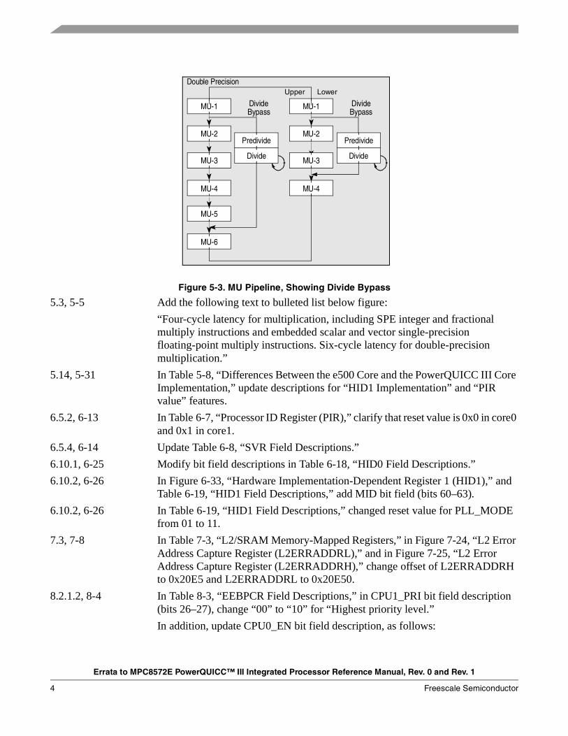
5.3, 5-5 Modify Figure 5-3, “MU Pipeline, Showing Divide Bypass,” as follows:
Table 4-39. Engineering Use POR Config Signal
External Signal Config Signal
MSRCID[1] cfg_eng_use[1]
Errata to MPC8572E PowerQUICC™ III Integrated Processor Reference Manual, Rev. 0 and Rev. 1
4 Freescale Semiconductor
Figure 5-3. MU Pipeline, Showing Divide Bypass
5.3, 5-5 Add the following text to bulleted list below figure:
“Four-cycle latency for multiplication, including SPE integer and fractional multiply instructions and embedded scalar and vector single-precision floating-point multiply instructions. Six-cycle latency for double-precision multiplication.”
5.14, 5-31 In Table 5-8, “Differences Between the e500 Core and the PowerQUICC III Core Implementation,” update descriptions for “HID1 Implementation” and “PIR value” features.
6.5.2, 6-13 In Table 6-7, “Processor ID Register (PIR),” clarify that reset value is 0x0 in core0 and 0x1 in core1.
6.5.4, 6-14 Update Table 6-8, “SVR Field Descriptions.”
6.10.1, 6-25 Modify bit field descriptions in Table 6-18, “HID0 Field Descriptions.”
6.10.2, 6-26 In Figure 6-33, “Hardware Implementation-Dependent Register 1 (HID1),” and Table 6-19, “HID1 Field Descriptions,” add MID bit field (bits 60–63).
6.10.2, 6-26 In Table 6-19, “HID1 Field Descriptions,” changed reset value for PLL_MODE from 01 to 11.
7.3, 7-8 In Table 7-3, “L2/SRAM Memory-Mapped Registers,” in Figure 7-24, “L2 Error Address Capture Register (L2ERRADDRL),” and in Figure 7-25, “L2 Error Address Capture Register (L2ERRADDRH),” change offset of L2ERRADDRH to 0x20E5 and L2ERRADDRL to 0x20E50.
8.2.1.2, 8-4 In Table 8-3, “EEBPCR Field Descriptions,” in CPU1_PRI bit field description (bits 26–27), change “00” to “10” for “Highest priority level.”
In addition, update CPU0_EN bit field description, as follows:
Upper Lower
MU-3
MU-1
MU-2
Divide Bypass Path
Postdivide
Divide
ReservationStation
From GIQ0 or GIQ1
MU-4
Upper Lower
MU-3
MU-1
MU-4
MU-2
Divide
Divide
Predivide
Bypass
MU-3
MU-1
MU-4
MU-2
Divide
Divide
Predivide
Bypass
MU-5
MU-6
Double Precision
Errata to MPC8572E PowerQUICC™ III Integrated Processor Reference Manual, Rev. 0 and Rev. 1
Freescale Semiconductor 5
“CPU0 port enable. Controls boot holdoff mode when the device is an agent of an external host or when the other core is used to perform initialization prior to allowing this core to boot. Specifies whether the e500 core (CPU) port0 is enabled to run transactions on the CCB. The CPU boot configuration power-on reset pin (cfg_cpu0_boot) determines the initial value of this bit. If the pin is sampled as a logic 1 at the negation of reset, CPU0 is enabled to boot at the end of the POR sequence. Otherwise, CPU0 cannot fetch its boot vector until an external host or another core sets the CPU0_EN bit.
0 Boot holdoff mode. CPU0 arbitration is disabled on the CCB and no bus grants are issued.
1 CPU0 is enabled and receives bus grants in response to bus requests for the boot vector.
After this bit is set, it should not be cleared by software. It is not intended to dynamically enable and disable CPU operation. It is only intended to end boot holdoff mode. See Section 4.4.3.7, “CPU Boot Configuration,” for more information.”
Chapter 9 Change “Dn_MAPAR_IN” to “Dn_MAPAR_ERR” throughout.
9.3.1, 9-3 Under Table 9-1, “DDR Memory Interface Signal Summary,” add the following text:
“Note that some devices implementing two DDR controllers may share one set of MDVAL and MSRCID[0:4] signals between them. Please refer to the signals and debug chapters for clarification on implementation.”
9.3.2.2, 9-11 In Table 9-4, “Clock Signals—Detailed Signal Descriptions,” update MCKE description with the following:
“The MCKE signals should be connected to the same rank of memory as the corresponding MCS and MODT signals. For example, MCKE[0] should be connected to the same rank of memory as MCS[0] and MODT[0].”
9.4, 9-11 In Table 9-5, “DDR Memory Controller Memory Map,” change reset value for DDR_IP_REV2 to 0x00nn_00nn.
9.4.1.2, 9-14 In Table 9-7, “CSn_CONFIG Field Descriptions,” modify sentence in ODT_RD_CFG and ODT_WR_CFG field descriptions, as follows: “ODT should only be used with DDR2 or DDR3.”
9.4.1.6, 9-21 In Table 9-11, “TIMING_CFG_1 Field Descriptions,” and in Table 9-12, “TIMING_CFG_2 Field Descriptions,” modify for the following bit field descriptions: WRREC, WRTORD, and RD_TO_PRE to add requirement for on-the-fly burst chop mode.
9.4.1.7, 9-23 In Figure 9-8, “DDR SDRAM Timing Configuration 2 Register (TIMING_CFG_2),” and Table 9-12, “TIMING_CFG_2 Field Descriptions,” change bits 4–8 CPO to Reserved.
Errata to MPC8572E PowerQUICC™ III Integrated Processor Reference Manual, Rev. 0 and Rev. 1
6 Freescale Semiconductor
9.4.1.9, 9-28 In Table 9-13, “DDR_SDRAM_CFG Field Descriptions,” add the following note to bit fields RD_EN and 2T_EN: “Note that RD_EN and 2T_EN must not both be set at the same time.”
9.4.1.9, 9-28 In Table 9-13, “DDR_SDRAM_CFG Field Descriptions,” add new programming requirement for HSE bit field description, as follows:
“Sets I/O driver impedance to half strength.
This impedance will be used by the MDIC,address/command, data, and clock impedance values, but only if automatic hardware calibration is disabled and the corresponding group's software override is disabled in the DDR control drive register(s) described in Section 9.4.1.24, “DDR Control Driver Register 1 (DDRCDR_1).”
9.4.1.14, 9-35 Change introduction to Figure 9-15, “DDR SDRAM Data Initialization Configuration Register (DDR_DATA_INIT),” to say the following:
“The DDR SDRAM data initialization register, shown in Figure 9-15, provides the value that is used to initialize memory if DDR_SDRAM_CFG2[D_INIT] is set.”
9.4.1.24, 9-46 Remove last sentence of second paragraph.
In addition, in the list of 4-bit impedance settings in this section, place text “default full-strength impedance” next to the “1010” for DDR2 and the “0111” for DDR3; add note after the DDR3 list stating that “0000” should be used for the default half-strength value.
In addition, modify the last paragraph (before DDRCDR_1 register figure) to say the following:
“A value of 0000 should be used for default half-strength mode when driver calibration is not used.
Note that the drivers may either be calibrated to full-strength or half-strength.”
9.4.1.27, 9-50 In Figure 9-28, “DDR IP Block Revision 2 (DDR_IP_REV2),” change reset value to “0000_0000_nnnn_nnnn_0000_0000_nnnn_nnnn.”
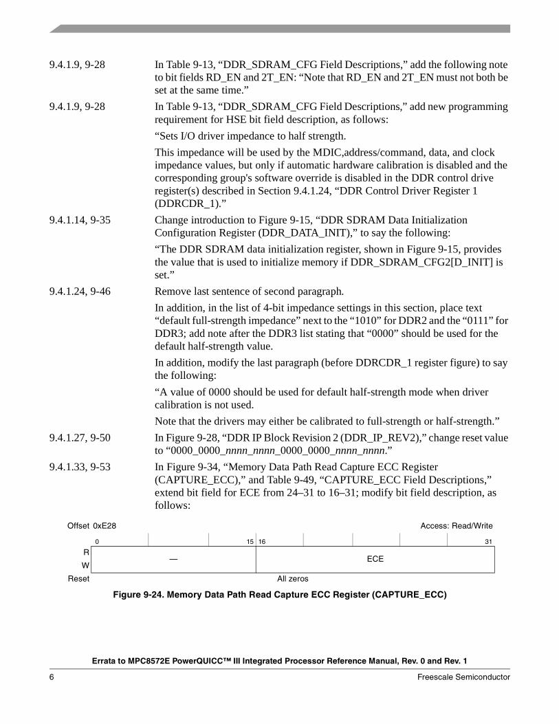
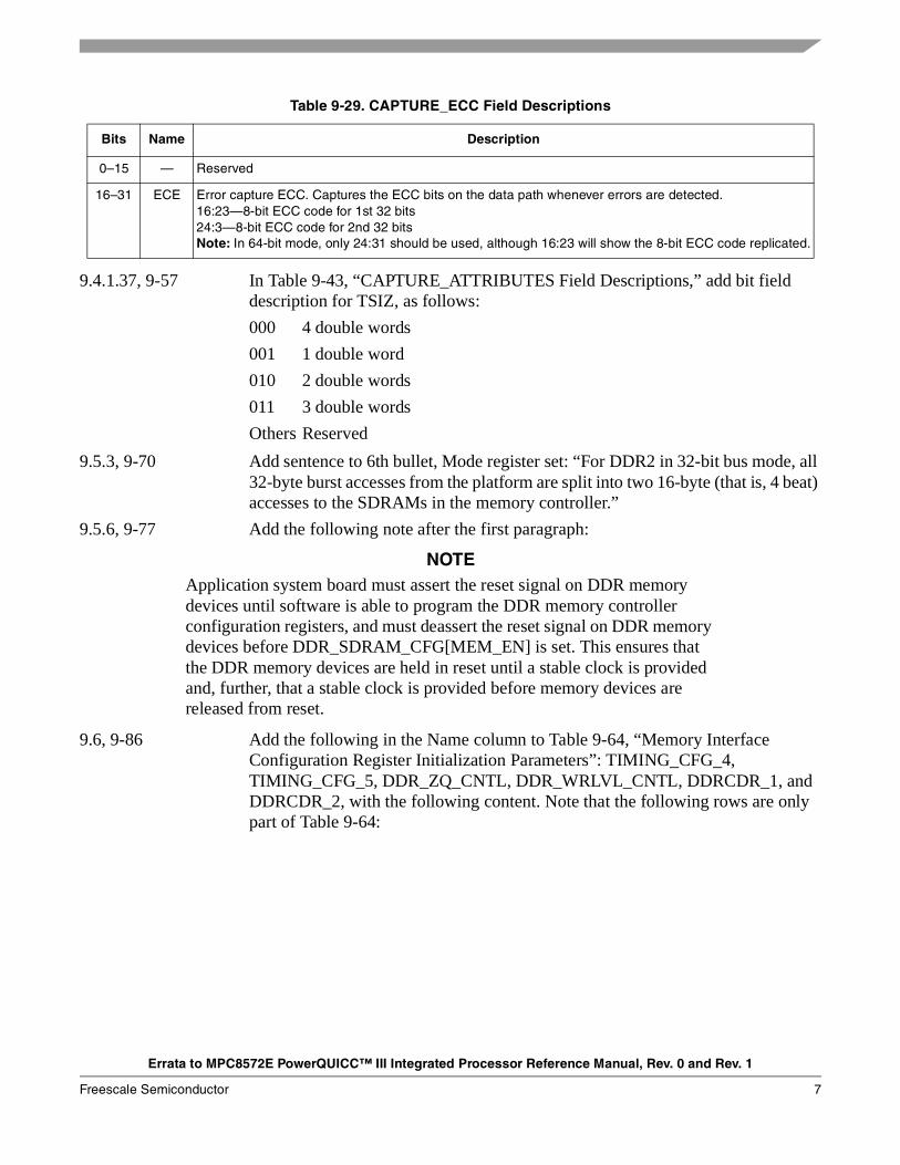
9.4.1.33, 9-53 In Figure 9-34, “Memory Data Path Read Capture ECC Register (CAPTURE_ECC),” and Table 9-49, “CAPTURE_ECC Field Descriptions,” extend bit field for ECE from 24–31 to 16–31; modify bit field description, as follows:
Offset 0xE28 Access: Read/Write
0 15 16 31
R— ECE
W
Reset All zeros
Figure 9-24. Memory Data Path Read Capture ECC Register (CAPTURE_ECC)
Errata to MPC8572E PowerQUICC™ III Integrated Processor Reference Manual, Rev. 0 and Rev. 1
Freescale Semiconductor 7
9.4.1.37, 9-57 In Table 9-43, “CAPTURE_ATTRIBUTES Field Descriptions,” add bit field description for TSIZ, as follows:
000 4 double words
001 1 double word
010 2 double words
011 3 double words
Others Reserved
9.5.3, 9-70 Add sentence to 6th bullet, Mode register set: “For DDR2 in 32-bit bus mode, all 32-byte burst accesses from the platform are split into two 16-byte (that is, 4 beat) accesses to the SDRAMs in the memory controller.”
9.5.6, 9-77 Add the following note after the first paragraph:
NOTEApplication system board must assert the reset signal on DDR memory devices until software is able to program the DDR memory controller configuration registers, and must deassert the reset signal on DDR memory devices before DDR_SDRAM_CFG[MEM_EN] is set. This ensures that the DDR memory devices are held in reset until a stable clock is provided and, further, that a stable clock is provided before memory devices are released from reset.
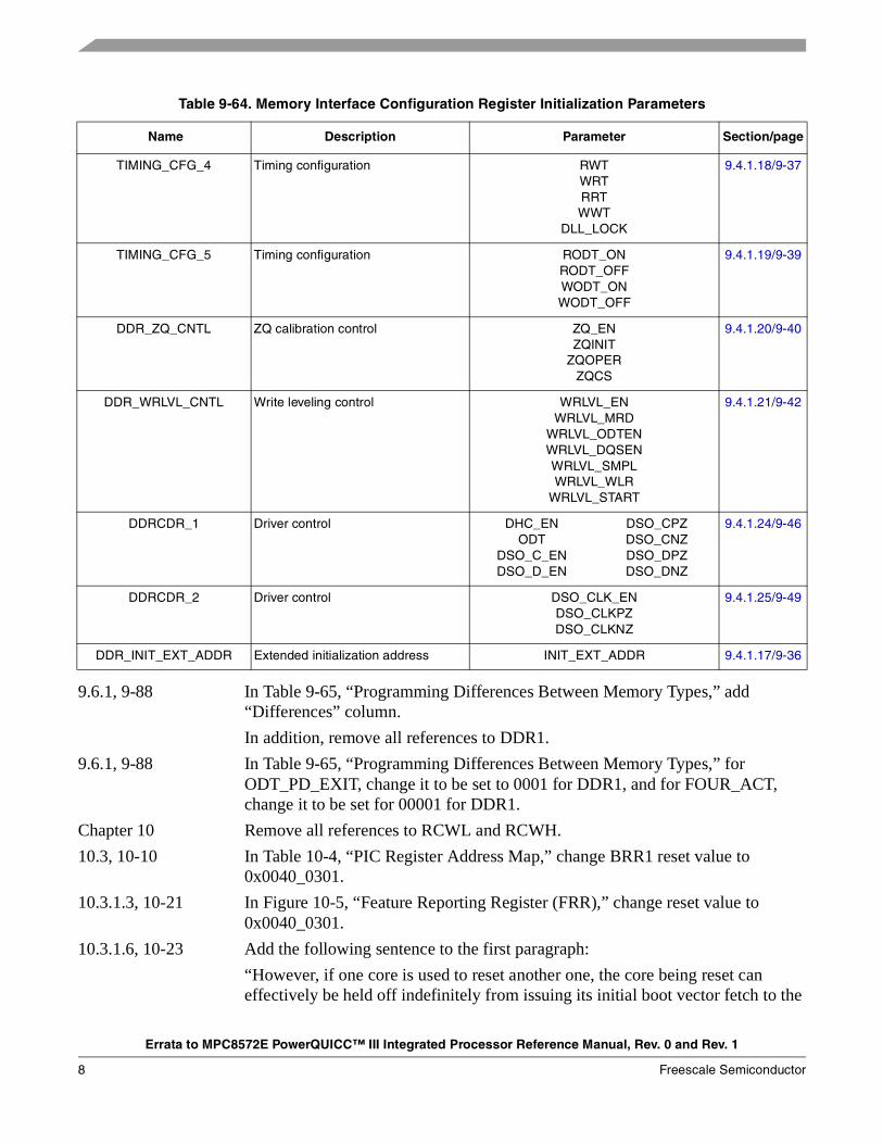
9.6, 9-86 Add the following in the Name column to Table 9-64, “Memory Interface Configuration Register Initialization Parameters”: TIMING_CFG_4, TIMING_CFG_5, DDR_ZQ_CNTL, DDR_WRLVL_CNTL, DDRCDR_1, and DDRCDR_2, with the following content. Note that the following rows are only part of Table 9-64:
Table 9-29. CAPTURE_ECC Field Descriptions
Bits Name Description
0–15 — Reserved
16–31 ECE Error capture ECC. Captures the ECC bits on the data path whenever errors are detected.16:23—8-bit ECC code for 1st 32 bits24:3—8-bit ECC code for 2nd 32 bitsNote: In 64-bit mode, only 24:31 should be used, although 16:23 will show the 8-bit ECC code replicated.
Errata to MPC8572E PowerQUICC™ III Integrated Processor Reference Manual, Rev. 0 and Rev. 1
8 Freescale Semiconductor
9.6.1, 9-88 In Table 9-65, “Programming Differences Between Memory Types,” add “Differences” column.
In addition, remove all references to DDR1.
9.6.1, 9-88 In Table 9-65, “Programming Differences Between Memory Types,” for ODT_PD_EXIT, change it to be set to 0001 for DDR1, and for FOUR_ACT, change it to be set for 00001 for DDR1.
Chapter 10 Remove all references to RCWL and RCWH.
10.3, 10-10 In Table 10-4, “PIC Register Address Map,” change BRR1 reset value to 0x0040_0301.
10.3.1.3, 10-21 In Figure 10-5, “Feature Reporting Register (FRR),” change reset value to 0x0040_0301.
10.3.1.6, 10-23 Add the following sentence to the first paragraph:
“However, if one core is used to reset another one, the core being reset can effectively be held off indefinitely from issuing its initial boot vector fetch to the
Table 9-64. Memory Interface Configuration Register Initialization Parameters
Name Description Parameter Section/page
TIMING_CFG_4 Timing configuration RWTWRTRRTWWT
DLL_LOCK
9.4.1.18/9-37
TIMING_CFG_5 Timing configuration RODT_ONRODT_OFFWODT_ONWODT_OFF
9.4.1.19/9-39
DDR_ZQ_CNTL ZQ calibration control ZQ_ENZQINIT
ZQOPERZQCS
9.4.1.20/9-40
DDR_WRLVL_CNTL Write leveling control WRLVL_ENWRLVL_MRD
WRLVL_ODTENWRLVL_DQSENWRLVL_SMPLWRLVL_WLR
WRLVL_START
9.4.1.21/9-42
DDRCDR_1 Driver control DHC_ENODT
DSO_C_ENDSO_D_EN
DSO_CPZDSO_CNZDSO_DPZDSO_DNZ
9.4.1.24/9-46
DDRCDR_2 Driver control DSO_CLK_ENDSO_CLKPZDSO_CLKNZ
9.4.1.25/9-49
DDR_INIT_EXT_ADDR Extended initialization address INIT_EXT_ADDR 9.4.1.17/9-36
Errata to MPC8572E PowerQUICC™ III Integrated Processor Reference Manual, Rev. 0 and Rev. 1
Freescale Semiconductor 9
platform by leaving its appropriate PIR[Px] bit asserted. Clearing it releases the core to fetch.”
10.3.6.3, 10-40 In Figure 10-33, “Shared Message Signaled Interrupt Index Register (MSIIR),” and in Table 10-35, “MSIIR Field Descriptions,” change SRS field to bits 0–2 and IBS field to bits 3–7.
11.1.4.7, 11-12 Modify section, as follows:
“The KEU (Kasumi Execution Unit) is a functional block capable of encrypting/decrypting and/or performing integrity checks on 64-bit blocks of data using a 128-bit key. The KEU is designed support the following cryptographic algorithms:
• f8 as defined in the ETSI/SAGE Specification Document 1 for the 3GPP standard
• f9 as defined in the ETSI/SAGE Specification Document 1 for the 3GPP standard
• A5/3 for GSM/EDGE
• GEA3 for GPRS
With the exception of f9, which is an authentication algorithm, KEU implements confidentiality algorithms. For f9, if the KEU is supplied with a MAC value, it is capable of performing a bitwise check of this original MAC against an f9 MAC generated by the KEU (ICV checking).
For more information, refer to Section 11.7.5, “Kasumi Execution Unit (KEU).’”
11.7.8.4, 11-162 In Figure 11-101, “RNGU Status Register,” change reset value from 0x003 to 0x01.
11.7.8.9, 11-166 Add the following note to end of section:
NOTE
Host reads of the RNGB FIFO should be performed on an 8-byte basis, regardless of how many bits of random number is actually required. Partial host reads can leave the RNGB FIFO in a state that results in a channel error.
Chapter 12 Change all instances of “E2PROM” to “EEPROM.”
12.3.1.2, 12-6 In Figure 12-3, “I2C Frequency Divider Register (I2CFDR),” changed reset value to All zeros; in Table 12-5, “I2CFDR Field Descriptions,” revise FDR (bits 2–7) field description.
12.3.1.4, 12-9 In Table 12-7, “I2CSR Field Descriptions,” change I2CSR to I2CDR for the received case conditions in MCF bit field description.
12.3.1.5, 12-10 In Table 12-8, “I2CDR Field Descriptions,” modify last sentence of DATA bit field description to say, “Note that in both master receive and slave receive modes, the very first read is always a dummy read.”
12.4.5, 12-17 Modify first paragraph as follows:
Errata to MPC8572E PowerQUICC™ III Integrated Processor Reference Manual, Rev. 0 and Rev. 1
10 Freescale Semiconductor
“If boot sequencer mode is selected on POR (by the settings on the cfg_boot_seq[0:1] reset configuration signals, as described in Section 4.4.3.8, “Boot Sequencer Configuration”), the I2C1 module communicates with one or more EEPROMs through the I2C interface on IIC1_SCL and IIC1_SDA. The boot sequencer accesses the I2C1 serial ROM device at a serial bit clock frequency equal to the platform (CCB) clock frequency divided by 2560. The EEPROM(s) can be programmed to initialize one or more configuration registers of this integrated device.”
12.4.5, 12-17 Remove sentence, “For 1-byte transfers, a dummy read should be performed by the interrupt service routine.”
Chapter 13 Replace “CCB clock” with “platform clock,” throughout.
13.1.2, 13-2 Remove the DUART Signal Overview table.
Chapter 14 Remove section, “Multiplexed Address/Data Bus for 26-Bit Addressing.”
In addition, add overbar all active low signals LCSn.
14.1.3, 14-3 Modify the section, as follows:
“The eLBC provides one GPCM, one FCM, and three UPMs for the local bus, with no restriction on how many of the eight banks (chip selects) can be programmed to operate with any given machine. The internal transaction address is limited to 32 bits, so all chip selects must fall within the 4-Gbyte window addressed by the internal transaction address. When a memory transaction is dispatched to the eLBC, the internal transaction address is compared with the address information of each bank (chip select). The corresponding machine assigned to that bank (GPCM, FCM, or UPM) then takes ownership of the external signals that control the access and maintains control until the transaction ends. Thus, with the eLBC in GPCM or FCM, or UPM mode, only one of the eight chip selects is active at any time for the duration of the transaction except in the case of UPM refresh where all UPM machines that are enabled for refresh have concurrent chip select assertion.”
14.2, 14-4 In Table 14-1, “Enhanced Local Bus Controller Detailed Signal Descriptions,” change wording of LGPLn timing description to say its value is driven.
14.2, 14-4 In Table 14-1, “Enhanced Local Bus Controller Detailed Signal Descriptions,” modify the signal description of LBCTL to say the following:
“The memory controller activates LBCTL for the local bus when a GPCM-, UPM-, or FCM-controlled bank is accessed. Buffer control is disabled by setting ORn[BCTLD].”
In addition, modify LA signal addressing and change state meaning to the following: “LA is the address bus used to transmit addresses to external RAM devices. Refer to Section 14.5, “Initialization/Application Information,” for address signal multiplexing.”
14.3.1.1, 14-11 In Table 14-4, “BRn Field Descriptions,” add the following sentence to DECC (bits 21–22) field description: “The reset value of this field is configured during power-on reset by the signal, cfg_fcm_ecc.”
Errata to MPC8572E PowerQUICC™ III Integrated Processor Reference Manual, Rev. 0 and Rev. 1
Freescale Semiconductor 11
14.3.1.1, 14-11 In Table 14-4, “BRn Field Descriptions,” clarify PS field description with respect to FCM capabilities, as follows:
“10 16-bit (not supported for FCM)
11 32-bit (not supported for FCM)”
14.3.1.2, 14-13 Move Table 14-5, “Reset value of OR0 Register,” to Section 14.3.1.2, “Option Registers (OR0–OR7).”
14.3.1.4, 14-22 In Table 14-11, “MxMR Field Descriptions,” modify AM (bits 5–7) field description, as follows:
“Address multiplex size. Determines how the address of the current memory cycle can be output on the address pins. This field is needed when interfacing with devices requiring row and column addresses multiplexed on the same pins. See Section 14.4.4.4.7, “Address Multiplexing (AMX)” for more information.
000 Internal transaction address a[8:23] driven on [16:31]; LAD[0:15] driven low.
001 Internal transaction address a[7:22] driven on [16:31]; LAD[0:15] driven low.
010 Internal transaction address a[6:21] driven on [16:31]; LAD[0:15] driven low.
011 Internal transaction address a[5:20] driven on [16:31]; LAD[0:15] driven low.
100 Internal transaction address a[4:19] driven on [16:31]; LAD[0:15] driven low.
101 Internal transaction address a[3:18] driven on [16:31]; LAD[0:15] driven low.
110 Reserved
111 Reserved”
14.3.1.7, 14-25 Update second part of first paragraph, as follows:
“To avoid race conditions between software and a busy eLBC, registers that affect currently running special operation and LSOR must not be re-written before a pending special operation has been completed. The UPM and FCM have different indications of when such special operations are completed. The behavior of eLBC is unpredictable if special operation modes are altered between LSOR being written and the relevant memory controller completing that access.”
14.3.1.9, 14-27 Change first sentence to say, “The transfer error status register (LTESR) indicates the cause of an error or event.”
14.3.1.15, 14-34 In Table 14-22, “LCRR Field Descriptions,” revise description for CLKDIV to say system clock is equivalent to ccb_clk and deleted statement about twice the csb_clk.
In addition, modify PBYP (bit 0) field description, as follows:
“PLL bypass. This bit should be set when using low bus clock frequencies (See device hardware specifications for applicable frequencies.). When in PLL bypass mode, incoming data is captured in the middle of the bus clock cycle.
0 The PLL is enabled.
1 The PLL is bypassed.”
Errata to MPC8572E PowerQUICC™ III Integrated Processor Reference Manual, Rev. 0 and Rev. 1
12 Freescale Semiconductor
14.3.1.16, 14-35 In Table 14-22, “FMR Field Descriptions,” in CWTO (bits 16–19) field description, change “(CW0–CW3)” to “(CW0, CW1, RBW and RSW).”
14.4.2.1, 14-50 In Table 14-31, “GPCM Read Control Signal Timing,” update tARCS and tCSRP field so they match the RTL behavior.
14.4.2.2, 14-52 In Table 14-31, “GPCM Write Control Signal Timing,” update tAWCS, tCSWP and tWC so they match the RTL behavior.
14.4.2.3.2, 14-55 Modify sentence in first number of numbered list, as follows: “ORn[CSNT], along with ORn[TRLX], control the timing for the appropriate strobe negation in write cycles.”
14.4.3.4.2, 14-75 Revise steps 3 and 4 in the numbered list.
14.4.4.4.1, 14-82 In Figure 14-65, “RAM Word Field Descriptions,” add the following note to LOOP and AMX bit field descriptions: “AMX must not change values in any RAM word which begins a loop.”
14.4.4.4.5, 14-87 Add the following to the bulleted list: “Loop start word should not have an AMX change with regard to the previous word.”
14.4.4.4.7, 14-88 Modify the note to say: “AMX must not change values in any RAM word which begins a loop.”
14.4.4.4.7, 14-88 Modify last two sentences of first paragraph to say the following:
“The next address (NA) bit of the RAM word does not affect LA signals, unless AMX = 00 and chooses the column address for NA = 1.”
14.4.4.5, 14-91 Add the following conditions to the end of the second paragraph:
“The conditions are as follows:
• The PLL must be enabled, that is, LCRR[PBYP] = 0.
• DLT3 bit must be cleared in the same RAM word to avoid mid-sampling of read data.
• LBCR[LPBSE] = 0 and MXMR[GPL4] = 1
• The combination WAEN=1 and UTA=1 should be in the RAM word next to the word which gets frozen by LUPWAIT assertion. This condition limits the use of this mode to cases where the exact cycle of LUPWAIT assertion is predictable.”
14.5.1, 14-92 Remove the following text:
“The local bus can be used either with separate address and data buses or with a multiplexed address/data bus. A full 32-bit address or the lower 26 bits of the address can be provided according to the size of memory devices and pin count limitations.”
14.5.1.3, 14-93 Change the last sentence in the first paragraph below Figure 14-71, “GPCM Address Timings,” to say the following: “Typical values for the two propagation delays are in the order of 3–6 ns, so for a 133-MHz bus frequency, LCS should arrive on the order of 3 bus clocks later.”
14.5.4.5, 14-99 Add the following text to the beginning of the second paragraph:
Errata to MPC8572E PowerQUICC™ III Integrated Processor Reference Manual, Rev. 0 and Rev. 1
Freescale Semiconductor 13
“Note that operations specified by OP3 and OP4 (status read) should never be skipped while erasing a NAND Flash device, because, in case that happens, contention may arise on LGPL4.”
14.5.4.6, 14-100 Add the following text to the beginning of the second paragraph:
“Note that operations specified by OP5 and OP6 (status read) should never be skipped while programming a NAND Flash device, because, in case that happens, contention may arise on LGPL4.”
14.5.8, 14-106 Remove Section 14.5.8, “Interfacing to DSP Host Ports.”
15.3, 15-5 Modify first bullet’s content under “Ethernet and FIFO operation” as follows:
“The ECNTRL register’s FIFO mode enable bit (ECNTRL[FIFM]) allows bypass of the Ethernet MAC and enables I/O through the FIFO interface sharing the normal GMII signals. Each eTSEC supports an 8-bit FIFO interface independently. Pairs of GMII ports can be combined to create a 16-bit, full-duplex interface. If configured in FIFO mode, the FIFOCFG register determines operation. In FIFO mode data is transferred synchronously with respect to the external data clock. See the device hardware specifications document for maximum supported frequencies.”
15.4, 15-6 In Table 15-1, “eTSECn Network Interface Signal Properties,” and in Table 15-2, “eTSEC Signals—Detailed Signal Descriptions,” change “EC2_MDC” and “EC2_MDIO” to “EC3_MDC” and “EC3_MDIO.”
In addition, add MII to designated modes during which TXD[7:4] and RXD[7:4] are unused.
In addition, for RGMII and RTBI protocols, change description of TSEC_RX_ER from “Unused, output driven low” to “Unused.”
In addition, remove references to TSEC_1588_PP3 signal and to TMR_TEMASK[PP3EN].
15.4.1, 15-9 In Table 15-2, “eTSEC Signals—Detailed Signal Descriptions,” change the State Meaning description for TSECn_CRS, as follows:
“Asserted/Negated—In MII mode, TSECn_CRS is asserted while the transmit or receive medium is not idle. In the event of a collision, TSECn_CRS must remain asserted for the duration of the collision.”
15.4.1, 15-9 In Table 15-2, “eTSEC Signals—Detailed Signal Descriptions,” remove the following sentence from TSECn_GTX_CLK description:
“In RMII mode, TSECn_GTX_CLK feeds back the effective transmit clock according to the interface, 100Base-T is 25 MHz and 10Base-T is 2.5 MHz.”
15.4.1, 15-9 In Table 15-2, “eTSEC Signals—Detailed Signal Descriptions,” modify TSECn_RX_CLK signal description, as follows:
“Receive clock. In GMII, MII, or RGMII mode, the receive clock TSECn_RX_CLK is a continuous clock (2.5, 25, or 125 MHz) that provides a timing reference for TSECn_RX_DV, TSECn_RXD, and TSECn_RX_ER.
Errata to MPC8572E PowerQUICC™ III Integrated Processor Reference Manual, Rev. 0 and Rev. 1
14 Freescale Semiconductor
In TBI mode, TSECn_RX_CLK is the input for a 62.5 MHz PMA receive clock, 0 split phase with PMA_RX_CLK1 and is supplied by the SerDes.
In RTBI mode it is a 125-MHz receive clock.
In RMII mode this clock is not used for the receive clock, as RMII uses a shared reference clock.
However, note that due to pin limitations on the MPC8572E, eTSEC4 must be configured differently from the other eTSECs in RMII mode. For eTSEC1–3, the RMII reference clock is obtained from TSECn_TX_CLK. For eTSEC4, however, this clock comes from TSEC4_RX_CLK (TSEC3_COL).
In FIFO mode the receive clock is a continuous clock. See the device hardware specifications document for maximum supported frequencies.”
15.4.1, 15-9 In Table 15-2, “eTSEC Signals—Detailed Signal Descriptions,” modify TSECn_TX_CLK signal description, as follows:
“Transmit clock in. In MII mode, TSECn_TX_CLK is a continuous clock (2.5 or 25 MHz) that provides a timing reference for the TSECn_TX_EN, TSECn_TXD, and TSECn_TX_ER signals.
In GMII mode, this signal provides the 2.5 or 25 MHz timing reference during 10Base-T and100Base-T and comes from the PHY. In 1000Base-T this clock is not used and TSECn_GTX_CLK (125 MHz) becomes the timing reference. The TSECn_GTX_CLK is generated in the eTSEC and provided to the PHY and the MAC. The TSECn_TX_CLK is generated in the PHY and provided to the MAC.
In TBI mode, this signal is PMA receive clock 1 at 62.5 MHz, split phase with PMA_RX_CLK0, and is supplied by the SerDes.
In RMII mode this signal is the reference clock shared between transmit and receive, and is supplied by the PHY.
In FIFO mode the transmit clock is a continuous clock. See the device hardware specifications document for maximum supported frequencies.
This signal is not used in the eTSEC RTBI or RGMII modes.”
15.4.1, 15-9 In Table 15-2, “eTSEC Signals—Detailed Signal Descriptions,” change TSECn_TX_EN signal description from “rising and falling edges of the TSECn_TX_CLK, respectively” to “rising and falling edges of the TSECn_GTX_CLK, respectively.”
15.5.3.1.3, 15-28 In Figure 15-4, “IEVENT Register Definition,” and in Table 15-7, “IEVENT Field Descriptions,” add FGPI (bit 27) field. The bit field description is as follows:
“Filer generated general purpose interrupt on a set of filer rule match. This bit is set upon reception of a frame that matches a GPI rule sequence that is specified in the filer. It is synchronized with the setting of RXF.
0 No filer generated interrupt has occurred.
1 The filer has accepted a frame via a matching rule that the RQFCR[GPI] bit set.”
Errata to MPC8572E PowerQUICC™ III Integrated Processor Reference Manual, Rev. 0 and Rev. 1
Freescale Semiconductor 15
15.5.3.1.4, 15-32 In Figure 15-5, “IMASK Register Definition,” and in Table 15-8, “IMASK Field Descriptions,” add FGPIEN (bit 27) field.
15.5.3.2.1, 15-41 In Table 15-15, “TCTRL Field Descriptions,” modify TFC_PAUSE (bit 28) field description, as follows:
“Transmit flow control pause frame. Set this bit to transmit a PAUSE frame. If this bit is set, the MAC stops transmission of data frames after the currently transmitting frame completes. Next, the MAC transmits a pause control frame with the duration value obtained from the PTV register. The TXC event occurs after sending the pause control frame. Finally, the controller clears TFC_PAUSE and resumes transmitting data frames as before. Note that pause control frames can still be transmitted if the Tx controller is stopped due to user assertion of DMACTRL[GTS] or reception of a PAUSE frame. 0 No request for Tx PAUSE frame pending or transmission complete. 1 Software request for Tx PAUSE frame pending.”
15.5.3.2.2, 15-42 Modify section to say the following:
“This register is read/write-one-to-clear and is written by the eTSEC to convey DMA status information for each TxBD ring. The halt bit only has meaning for enabled rings. After processing transmit-related interrupts, software should use TSTAT to restart transmission from rings that may have been affected by the interrupt condition. In particular, an error condition that prevents eTSEC from continuing transmission halts DMA from all rings, including the ring that gave rise to the error. Figure 15-12 describes the TSTAT register.”
15.5.3.2.4, 15-47 In Table 15-18, “TXIC Field Descriptions,” add the following footnote to ICCS bit field description : “The term ‘system clock’ refers to CCB clock/2.”
15.5.3.3.1, 15-54 In Figure 15-24, “RCTRL Register Definition” and Table 15-26, “RCTRL Field Descriptions,” add PRSFM (bit 26) field, as follows:
“FIFO-mode parsing
0 L2 parsing in FIFO mode is not available. Must be 0 for non-FIFO modes.
1 L2 parsing in FIFO mode is available”
15.5.3.3.1, 15-54 In Table 15-28, “RCTRL Field Descriptions,” modify bit field description for TS (bit 7), as follows:
“Time stamp incoming packets as padding bytes. PAL field is set to 8 if the PAL field is programmed to less than 8. Must be set to zero if TMR_CTRL[TE]=0.”
15.5.3.3.1, 15-54 In Table 15-28, “RCTRL Field Descriptions,” modify RSF (bit 29) field description, as follows:
“Receive short frame mode. When set, enables the reception of frames shorter than 64 bytes. For packets received over the FIFO packet interface, this bit has no effect (packets shorter than 64 bytes are always accepted).
0 Ethernet frames less than 64B in length are silently dropped.
1 Frames more than 16B and less than 64B in length are accepted upon a DA match.
Errata to MPC8572E PowerQUICC™ III Integrated Processor Reference Manual, Rev. 0 and Rev. 1
16 Freescale Semiconductor
Note that frames less than or equal to 16B in length are always silently dropped.”field is programmed to less than 8. Must be set to zero if TMR_CTRL[TE]=0.”
15.5.3.3.3, 15-59 In Table 15-30 “RXIC Field Descriptions,” add the following footnote to ICCS bit field description : “The term ‘system clock’ refers to CCB clock/2.”
15.5.3.3.5, 15-61 In Table 15-32, “RBIFX Field Descriptions,” modify [BnCTL]=01 field descriptions to clarify that arbitrary extraction of preamble is not supported in FIFO modes
15.5.3.3.7, 15-64 In Figure 15-30, “Receive Queue Filer Table Control Register Definition,” and in Table 15-34, “RQFCR Field Descriptions,” add GPI (bit 0) field. The bit field description is as follows:
General purpose interrupt. When a property matches the value in the RQPROP entry at this index, and REJ = 0 and AND = 0, the filer instructs the Rx descriptor controller to set IEVENT[FGPI] when the corresponding receive frame is written to memory.
If the timer is enabled (TMR_CTRL[TE] = 1), then TMR_PEVENT[RXP] is also set.
15.5.3.3.8, 15-65 In Table 15-35, “RQFPR Field Descriptions,” add the following text to IPF (bit 20) field description:
“See the descriptions of receive FCB fields IP and PRO in Section 18.6.4.3, “Receive Path Off-Load,” for more information on determining the status of received packets for which IPF is set.”
15.5.3.3.8, 15-65 In Table 15-35, “RQFPR Field Descriptions,” add the following text to ETY (bits 16–31) field description:
“Note that the eTSEC filer gets multiple packet attributes as a result of parsing the packet. The behavior of the eTSEC is that it pulls the innermost ethertype found in the packet; this means that in many supported protocols, it is impossible to create a filer rule that matches on the outer ethertype. There are four cases that need to be highlighted.
1. The jumbo ethertype (0x8870)—In this case, the eTSEC assumes that the following header is LLC/SNAP. LLC/SNAP has an associated Ethertype, and the ETY field is populated with that ethertype. This makes it impossible to file on jumbo frames. In this case, one can use arbitrary extracted bytes to pull the outermost Ethertype.
2. The PPPoE ethertype described above.
3. The VLAN tag ethertype (0x8100)—In this case, one can use the PID1 VLN bit to indicate that the packet had a VLAN tag.
4. The MPLS tagged packets. In this case, one can use arbitrary extraction bytes to compare to the actual ethertype if a filer rule is intending to file based on an MPLS label existence.”
In addition, add the following note to TOS bit field description (bits 24–31):

Errata to MPC8572E PowerQUICC™ III Integrated Processor Reference Manual, Rev. 0 and Rev. 1
Freescale Semiconductor 17
“Note that for IPv6 the Traffic Class field is extracted using the IP header definition in RFC 2460. IPv6headers formed using the earlier RFC 1883 have a different format and must be handled with software.”
15.5.3.5.2, 15-76 In Table 15-43, “MACCFG2 Field Descriptions,” modify Huge Frame (bit 26) bit field description and MPEN (bit 28) bit field description; clarify that TX preamble length may be from 0x3 to 0xF.
15.5.3.6.26, 15-101 In Table 15-83, “TPKT Field Descriptions,” change TPKT size to bits 10–31.
15.5.3.8.1, 15-117 In Table 15-108, “FIFOCFG Field Descriptions,” modify IPG (bits 8–15) field description, as follows:
“Minimum inter packet gap. This sets the minimum number of cycles inserted between back-to-back frames transmitted over the FIFO interface. The minimum required is 3 cycles if CRCAPP=0, 5 cycles for 16-bit interfaces if CRCAPP=1 and 7 cycles for 8-bit interfaces if CRCAPP=1.”
15.5.3.9.2, 15-120 In Figure 15-107, “ATTRELI Register Definition,” modify the size of EI (bits 18–25), and in Table 15-110, “ATTRELI Field Descriptions,” modify EI bit field description, as follows:
“Extracted index. Points to the first byte, as a multiple of 64 bytes, within the receive frame from which to begin extracting data.”
15.5.3.10.1, 15-121 Modified first paragraph to say the following:
“The RQPRMn registers specify the minimum number of BDs required to prevent flow control being asserted and the total number of Rx BDs in their respective ring. Whenever the free BD count calculated by the eTSEC for any active ring drops below the value of RQPRMn[FBTHR] for that ring, link level flow control is asserted. Software must not write to RQPRMn while LFC is enabled and the eTSEC is actively receiving frames. However, software may modify these registers after disabling LFC by clearing RCTRL[LFC]. Note that packets may be lost due to lack of RxBDs while RCTRL[LFC] is clear. Software can prevent packet loss by manually generating pause frames (via TCTRL[TFC_PAUSE]) to cover the time when RCTRL[LFC] is clear. Figure 15-104 describes the definition for the RQPRMn register.”
15.5.3.11, 15-122 Modify section, as follows:
“IEEE 1588 compatible timestamping on this device is accomplished using the per-port transmit timestamping registers within each Ethernet controller memory space (See Section 15.5.3.2.10, “Transmit Time Stamp Identification Register (TMR_TXTS1–2_ID),” and Section 15.5.3.2.11, “Transmit Time Stamp Register (TMR_TXTS1–2_H/L).”) in conjunction with the following common registers, which are located within the memory space for eTSEC1. Because the common 1588 timestamping registers exist within the eTSEC1 memory space, the eTSEC1 controller must remain enabled in order to use 1588 timestamping for any Ethernet port.”
15.5.3.11.1, 15-122 In Table 15-113, “TMR_CTRL Register Field Descriptions,” clarifiy description of CIPH (bit 25) field description, as follows:
Errata to MPC8572E PowerQUICC™ III Integrated Processor Reference Manual, Rev. 0 and Rev. 1
18 Freescale Semiconductor
“External oscillator input clock phase.
0 non-inverted frequency tuned timer input clock
1 inverted frequency tuned timer input clock (NOTE: this setting is reserved if CKSEL=01.)”
In addition, modify ETEP2 field description to say “External trigger 2 edge polarity” (was “External trigger 1 edge polarity”), and ETEP1 field description to say “External trigger 1 edge polarity” (was “External trigger 2 edge polarity”).
15.5.3.11.1, 15-122 In Table 15-113, “TMR_CTRL Register Field Descriptions,” add the following note to TMSR (bit 26) bit field description:
“Note: Prior to initiating timer reset (setting TMSR), must gracefully stop receiver (See MACCFG1[RX_EN] description). User programmable registers are not reset by the soft reset; for example, TMR_CTRL, TMR_TEMASK, TMR_PEMASK, TMR_ADD, TMR_PRSC, TMROFF_H/L, TMR_ALARMn, and TMR_FIPERn.”
15.5.3.11.3, 15-125 Remove references to TSEC_1588_PP3 signal and to TMR_TEMASK[PP3EN].
15.5.3.11.11, 15-131 Add the following note:
NOTEAll TMROFF_H registers in a device should be set to the same value, and all TMROFF_L registers in a device should be set to the same value. Otherwise, the precision time protocol may not work.
In addition, remove the following sentence:
“This allows each Ethernet channel to have a different timebase offset from the central TMR_CNT_H/L.”
15.5.3.11.12, 15-131 In Table 15-126, “TMR_ALARMn_H/L Register Field Descriptions,” modify the first paragraph of ALARM_H/L bit field description, as follows:
“Alarm time comparator register. The corresponding alarm event in TMR_TEVENT is set when the current time counter becomes equal to or greater than this alarm time compare value in TMR_ALARMn_L/H. Writing the TMR_ALARMn_L register deactivates the alarm event after it has fired. Writing the TMR_ALARMn_L followed by the TMR_ALARMn_H register rearms the alarm function with the new compare value.”
15.5.4.3.10, 15-145 In Table 15-140, “TBICON Field Descriptions,” modify Clock Select (bit 10) field description, as follows:
“Clock select. This bit is cleared by default.
0 Allow the TBI to accept dual split-phase 62.5 MHz receive clocks.
1 Configure the TBI to accept a 125 MHz receive clock from the SerDes/PHY. The 125 MHz clock must be physically connected to ‘PMA receive clock 0’ if using a parallel (non-SGMII) Ethernet protocol.”
15.6.1.8, 15-157 Add Section 15.6.1.8, “SGMII Interface,” as follows:
Errata to MPC8572E PowerQUICC™ III Integrated Processor Reference Manual, Rev. 0 and Rev. 1
Freescale Semiconductor 19
“SGMII communication using the eTSEC is accomplished through the SerDes interface. See Table 15-1 on page 15-7 for specific signal assignments.”
15.6.2, 15-157 Modify last bulleted item in section as follows:
“On transmission, the minimum inter-packet gap (set in FIFOCFG[IPG]) is three cycles if CRC is not automatically appended. Each CRC data beat adds to this requirement. For 16-bit FIFO interfaces the minimum Tx IPG is 5 cycles and for 8-bit FIFO interfaces the minimum is 7 cycles.”
15.6.3.2, 15-166 Change step 3 to say the following:
“Set SOFT_RESET bit in MACCFG1 register (Note that SOFT_RESET must remain set for at least 3 TX clocks before proceeding.)”
15.6.3.8, 15-175 Add sentence clarifying that sleep mode is not supported for Magic Packet in the first paragraph.
15.6.3.8, 15-175 Modify last sentence, as follows: “Only frames addressed specifically to the MAC’s station address or a valid multicast or broadcast address can be examined for the Magic Packet sequence.”
15.6.3.11, 15-179 Revise section, as follows:
If a station must transmit, it waits until the LAN becomes silent for a specified period (inter-frame gap, or IFG). The minimum inter-packet gap (IPG) time for back-to-back transmission is set by IPGIFG[Back-to-Back Inter-Packet-Gap]. The receiver receives back-to-back frames with the minimum interframe gap (IFG) as set in IPGIFG[Minimum IFG Enforcement]. If multiple frames are ready to transmit, the ethernet controller follows the minimum IPG as long as the following restrictions are met:
• The first TxBD pointer, TBPTRn, of any given frame is located at a 16-byte aligned address.
• Each TxBD[Data Length] is greater-than or equal to 64 bytes.
If the first TxBD alignment restriction is not met, the back-to-back IPG may be as many as 32 cycles. If the TxBD size restriction is not met, the back-to-back IPG may be significantly longer.
In half-duplex mode, after a station begins sending, it continually checks for collisions on the LAN. If a collision is detected, the station forces a jam signal (all ones) on its frame and stops transmitting. Collisions usually occur close to the beginning of a packet. The station then waits a random time period (back-off) before attempting to send again. After the back-off completes, the station waits for silence on the LAN (carrier sense negated) and then begins retransmission (retry) on the LAN. Retransmission begins 36 bit times after carrier sense is negated for at least 60 bit times. If the frame is not successfully sent within a specified number of retries, an error is indicated (collision retry limit exceeded).
15.6.3.13, 15-179 In Table 15-160, “Reception Errors,” remove the following note:
“Note: Any values in the length/type field between 1500 and 1536 will be treated as a length, however, only illegal packets exist with this length/type since these are
Errata to MPC8572E PowerQUICC™ III Integrated Processor Reference Manual, Rev. 0 and Rev. 1
20 Freescale Semiconductor
not valid lengths and not valid types. These are treated by the MAC logic as out of range.
Software must confirm the parser and filer results by checking the type/length field after the packet has been written to memory to see if it falls in this range.”
15.6.4.2, 15-182 In Table 15-161, “Tx Frame Control Block Description,” add the following sentence to PTP (bit 15) field description: “Must be clear if TMR_CTRL[TE] is clear.”
15.6.4.3, 15-184 In Table 15-162, “Rx Frame Control Block Descriptions,” add the following text to IP bit field descriptions (bit 1):
“If S/W is relying on the RxFCB for the parse results, any RxFCB[IP] bits set with the corresponding RxFCB[PRO] = 0xFF indicates a fragmented packet (or that this packet had a back-to-back IPv6 routing extension header). Additionally, RQFPR[IPF] (see Section 15.5.3.3.8, “Receive Queue Filer Table Property Register (RQFPR)”) indicates that the packet was fragmented.”
15.6.4.3, 15-184 In Table 15-162, “Rx Frame Control Block Descriptions,” add the following text to PRO bit field description (bits 8–15):
“Note that the eTSEC parser logic stops further parsing when encountering an IP datagram that has indicated that it has fragmented the upper layer protocol. This in general means that there is likely no layer 4 header following the IP header and extension headers. eTSEC leaves the RxFCB[PRO] and RQFPR[L4P] fields 0xFF in this case, which usually means that there was no IP header seen. In this case RxFCB[IP] and optionally RxFCB[IP6] is set. IP header checksumming operate sand perform as intended. Most of the time, the eTSEC updates the RxFCB[PRO] field and RQFPR[L4P] fileds with whatever value was found in the protocol field of the IP header. See Section 15.5.3.3.8, “Receive Queue Filer Table Property Register (RQFPR),” for a description of RQFPR.”
15.6.4.3, 15-184 In Table 15-162, “Rx Frame Control Block Descriptions,” replace “Layer 4 protocol identified according to IANA specification. Valid only if IP = 1,” in PRO bit field description with the following:
If IP = 1, PRO is set as follows:
• PRO=0xFF for a fragment header or a back to back route header
• PRO=0xnn for an unrecognized header, where nn is the next protocol field
• PRO=(TCP/UDP header), as defined in the IANA specification, if TCP or UDP header is found
If IP = 0, PRO is undefined.”
15.6.5.1.1, 15-187 Add the following statement to the bulleted list:
“The GPI field offers the user the ability to interrupt the core upon matching a rule that causes a frame to be filed to memory. Once the last RxBD corresponding to that frame is written to memory, the IEVENT[FGPI] event will be asserted. This bit will be set regardless of any interrupt coalescing that may be set.”
15.6.5.1.4, 15-189 Add the following paragraphs to end of section:
Errata to MPC8572E PowerQUICC™ III Integrated Processor Reference Manual, Rev. 0 and Rev. 1
Freescale Semiconductor 21
“A functional interrupt is provided via use of the general purpose interrupt (GPI) bit in the filer table. When a property matches the value in the RQPROP entry at this index, and REJ = 0 and AND = 0, the filer will set IEVENT[FGPI] when the corresponding receive frame is written to memory. This allows the user to set up a filer rule where the core will be interrupted upon the reception of ‘special’ frames.
If the timer is enabled (TMR_CTRL[TE] = 1), then the interrupt dedicated for timer events (in addition to the usual recieve, transmit and error interrupts) will be asserted.”
15.6.6.2.1, 15-196 Modify the last sentence of the note at the end of the section to say:
“As soon as the hardware consumes a BD (by writing it back to memory), RBPTRn advances and the free BD count reflects the correct number of available free BDs.”
15.6.7.4.1, 15-189 Remove Section 15.6.7.4.1, “Rx FCB Change.”
15.6.7.4.1, 15-200 Modify section as follows:
“The eTSEC receive filer has been enhanced with the addition of a general-purpose event bit. This event bit can be used in conjunction with filing table rules to identify 1588 packets and indicate these packets by setting special timer status register bits (TMR_STAT). Additionally, 1588 packets can be easily identified by upper-layer software by using the filer to queue all PTP packets to one or more predefined virtual queues. See Section 15.6.5.1.1, “Filing Rules,” for further information.”
15.6.8.1, 15-201 Replace sentence in first paragraph with the following:
“Because of pre-fetching, a minimum of four buffer descriptors per ring are required. This applies to both the transmit and the receive descriptor rings.”
removed statements about supporting 1588 on a per-eTSEC basis
15.6.8.2, 15-202 In Table 15-169, “Transmit Data Buffer Descriptor (TxBD) Field Descriptions,” modify TR bit field description.
15.6.8.3, 15-205 In Table 15-170, “Receive Buffer Descriptor Field Descriptions,” add the following sentence to Rx Data Buffer Pointer (bits 0–31) field description:
“For best performance, use 64-byte aligned receive buffer pointer addresses. The buffer must reside in memory external to the eTSEC.”
15.6.8.3, 15-205 In Table 15-170, Receive Buffer Descriptor Field Descriptions,” modify bit field descriptions for TR and LG.
15.7.1.7, 15-232 Remove references to TSEC4_RX_ER.
15.7.1.7, 15-232 In Table 15-189, “8-Bit FIFO Interface Mode Signal Configurations, eTSEC1/2,” in Table 15-190, “8-Bit FIFO Interface Mode Signal Configurations, eTSEC3/4,” and in Table 15-192, “16-Bit FIFO Interface Mode Signal Configuration (eTSECs1 and 2),” remove support for 3.3-V FIFO interface.
Errata to MPC8572E PowerQUICC™ III Integrated Processor Reference Manual, Rev. 0 and Rev. 1
22 Freescale Semiconductor
15.7.1.9, 15-238 Added Table 15-194, “SGMII Interface Signal Configuration (4-Wire),” to Section 15.7.1.9, “SGMII Interface Support.”
15.7.1.9, 15-238 In Table 15-195, “SGMII Mode Register Initialization Steps,” remove references to TBICON[Enable Wrap] and TBICON[Comma Detect].
15.7.1.9, 15-238 In Table 15-195, “SGMII Mode Register Initialization Steps,” modify row to say the following:
“Perform an MII Mgmt write cycle to TBI. Writing to MII Mgmt Control with 16-bit data intended for TBICON register, MIIMCON[0000_0000_0000_0000_0000_0000_0010_0000] This sets TBI in single clock mode and MII Mode off to enable communication with SerDes.”
Chapter 16 Replace “EC3_MDC” and “EC3_MDIO” with “EC5_MDC” and “EC5_MDIO” throughout.
16.4, 16-6 In second paragraph, change the signal count from “1” to “18.”
17.3.7.4, 17-55 In Table 17-59, “MIA_CR Field Descriptions,” update the bit field descriptions.
17.3.7.5, 17-56 In Table 17-60, “ MIA_ACR Field Descriptions,” update the bit field descriptions.
17.4.5.6, 17-174 Add Section 17.4.5.6, “Error Handling,” as follows:
“There are three types of errors that can be generated:
• No-halt errors
• Channel errors
• Common-control errors
No-halt errors are localized to the work unit itself and as a result dpes not cause the Pattern Matcher to halt operation. Channel and common-control errors are more severe, causing the Pattern Matcher to halt operations—on a specific channel in the case of channel errors, and on all channels for common-control errors.”
19.2.1, 19-5 Add the following note to Figure 19-3, “DMA Signal Summary”: “Note that this device does not support external control for every DMA channel.”
19.2.2, 19-5 In Table 19-3, “DMA Signals—Detailed Signal Descriptions,” clarify offering of external DMA signals.
19.3.1.1, 19-9 In Table 19-5, “MRn Field Descriptions,” remove the following sentence for bit field 4–7 BWC: “Defined only if MRn[EMP_EN] is set.”
19.3.1.1, 19-9 In Table 19-5, “MRn Field Descriptions,” modify CS (bit 31) field description, as follows:.
“Channel start. This bit is also automatically set by hardware during single-write start mode and external master start enable mode. Note that in external control mode, deasserting DMA_DREQ does NOT clear this bit.
0 Halt the DMA process if channel is busy (SRn[CB] is set). No effect if the channel is not busy.
Errata to MPC8572E PowerQUICC™ III Integrated Processor Reference Manual, Rev. 0 and Rev. 1
Freescale Semiconductor 23
1 Start the DMA process if channel is not busy (CB is cleared). If the channel was halted (CS = 0 and CB = 1), the transfer continues from the point at which it was halted.”
19.3.1.4, 19-15 Remove references to ATMU bypass mode for RapidIO.
19.3.1.6, 19-17 Remove references to ATMU bypass mode for RapidIO.
19.4.1.3, 19-33 Modify third paragraph, as follows:
“The external control and the DMA controller use a well defined protocol to communicate. The external control can start or restart a paused DMA transfer. The DMA controller acknowledges a DMA transfer in progress and also indicates a transfer completion.”
19.4.1.4, 19-32 Modify the first bullet in the bulleted list, as follows:
• DMA_DREQ - Asserting edge triggers a DMA transfer start or restart from a pause request. Sets MRn[CS]. (Note that negating DMA_DREQ does NOT clear MRn[CS].)
Modify second paragraph, as follows:
“If CC is set by software while the channel is busy with a transfer, the DMA controller finishes all transfers until it reaches the EOLND in basic mode or EOLSD in extended mode. The DMA controller then refetches the last link descriptor in basic mode, or the last list descriptor in extended mode and clears the channel continue bit. If EOLND or EOLSD is still set for their respective modes, the DMA controller remains in the idle state. If EOLND or EOLSD is not set, the DMA controller continues the transfer by refetching the new descriptor. The channel busy (SRn[CB]) bit is cleared when the DMA controller reaches EOLND/EOLSD and is set again when it initiates the refetch of the link or list descriptor.”
19.4.3, 19-35 Remove references to ATMU bypass mode for RapidIO.
19.4.5, 19-38 Remove references to ATMU bypass mode for RapidIO.
20.6.1.2, 20-11 In Table 20-2, “DICAR Field Description,” update DR field description, as follows:
“Device revision. This is a copy of the device’s system version register (SVR). See Section 23.4.1.16, “System Version Register (SVR),” for additional information.
0x80E8_0011 MPC8572E with security
0x80E0_0011 MPC8572 without security”
20.6.2.4, 20-23 In Table 20-19, “GCCSR Field Descriptions,” add the following parenthetical note to bit fields H, M, and D: “(Note that although this status bit is R/W, manually changing its value does not affect logical operation.)”
20.6.4.3, 20-37 In Table 20-33, “ECACSR Field Descriptions,” modify ECI (bits 8–23) field description, as follows:
“Extended capture information [0:15].
Errata to MPC8572E PowerQUICC™ III Integrated Processor Reference Manual, Rev. 0 and Rev. 1
24 Freescale Semiconductor
ECI contains the control/data character signal corresponding to each byte of captured data.
Each ECI bit reflects the validity of captured data. If a bit is set, then the designated byte of captured data is valid. If a bit is cleared, then the designated byte of the specified register does not contain valid data and should be disregarded until the bit is set.
ECI[0] reflects validity of PCSECCSR0[0:7]
ECI[1] reflects validity of PCSECCSR0[8:15]
ECI[2] reflects validity of PCSECCSR0[16:23]
ECI[3] reflects validity of PCSECCSR0[24:31]
ECI[4] reflects validity of PECCSR1[0:7]
ECI[5] reflects validity of PECCSR1[8:15]
...
ECI[14] reflects validity of PECCSR3[16:23]
ECI[15] reflects validity of PECCSR3[24:31]”
20.6.5.9, 20-47 In Figure 20-48, “Physical Configuration Register (PCR), make bit 27 CCP read/write.
20.6.7.9, 20-59 In Table 20-62, “RIWARn Field Descriptions,” modify TGINT bit field description to make 0011–1110 Reserved.
20.7.1.7, 20-69 In Table 20-72, “OMnDATR Field Descriptions,” references to “OMnMR[MM]” should instead reference “OMnDATR[MM].”
20.7.1.10, 20-71 References to “OMnMR[MM]” should instead reference “OMnDATR[MM].”
20.9.4.1, 20-141 References to “OMnMR[MM]” should instead reference “OMnDATR[MM].”
20.9.4.2.7, 20-153 References to “OMnMR[MM]” should instead reference “OMnDATR[MM].”
20.10.2.1.7, 20-171 In Table 20-130, “Outbound Doorbell Hardware Errors,” replace “ODMR[EIE]” with “OMnMR[EIE].”
21.1.1.1, 21-2 Add the following text to the end of the section:
“Note that after reset or when recovering from a link down condition, external transactions should not be attempted until the link has successfully trained. Software can poll the LTSSM state status register (PEX_LTSSM_STAT) to check the status of link training before issuing external requests.”
21.3.2.2, 21-11 Add the following text to the end of the first paragraph:
“Also note that accesses to the little-endian PCI Express configuration space must be properly formatted. See Section 21.4.1.2.1, “Byte Order for Configuration Transactions,” for more information.”
21.3.2.3, 21-11 In Table 21-6, “PEX_OTB_CPL_TOR Field Descriptions,” modify TC field description, as follows:
Errata to MPC8572E PowerQUICC™ III Integrated Processor Reference Manual, Rev. 0 and Rev. 1
Freescale Semiconductor 25
“Timeout counter. This is the value that is used to load the response counter of the completion timeout.
One TC unit is 8× the PCI Express controller clock period; that is, one TC unit is 20 ns at 400 MHz, and 30 ns at 266.66 MHz.
The following are examples of timeout periods based on different TC settings:
0x00_0000 Reserved
0x10_FFFF 22.28 ms at 400 MHz controller clock; 33.34 ms at 266.66 MHz controller clock
0xFF_FFFF 335.54 ms at 400 MHz controller clock; 503.31 ms at 266.66 MHz controller clock”
21.3.2.4, 21-12 In Table 21-7, “PEX_CONF_RTY_TOR Field Descriptions,” modify TC field description, as follows:.
“Timeout counter. This is the value that is used to load the CRS response counter.
One TC unit is 8× the PCI Express controller clock period; that is, one TC unit is 20 ns at 400 MHz and 30 ns at 266.66 MHz.
Timeout period based on different TC settings:
0x000_0000 Reserved
0x400_FFFF 1.34 s at 400 MHz controller clock, 2.02 s at 266.66 MHz controller clock
0xFFF_FFFF 5.37 s at 400 MHz controller clock, 8.05 s at 266.66 MHz controller clock”
21.3.2.5, 21-13 In Figure 21-6, “PCI Express Configuration Register (PEX_CONFIG),” and Table 21-8, “PEX_CONFIG Field Descriptions,” change IPOL (bit 16) to Reserved.
21.3.5.2.6, 21-28 In Table 21-22, “PCI Express Inbound Window Attributes Registers Field Descriptions,” modify TRGT bit field description to make 1101–1110 Reserved.
21.3.6.1, 21-30 In Table 21-23, “PCI Express Error Detect Register Field Descriptions,” add the following sentence to PCT (bit 8) field description: “Hot reset is recommended to restore stability of the system.”
21.3.6.4, 21-36 In Table 21-26, “PCI Express Error Capture Status Register Field Descriptions,” update GSID field description, as follows:
“Global source ID. This field indicates the internal platform global source ID that the error transaction originates. This field only applies to non PEX_CONFIG_ADDR/PEX_CONFIG_DATA transactions.
0 0000 PCI Express 3
0 0001 PCI Express 2
0 0010 PCI Express 1
0 1100 SRIO
0 1110 TLU 1, TLU 2
Errata to MPC8572E PowerQUICC™ III Integrated Processor Reference Manual, Rev. 0 and Rev. 1
26 Freescale Semiconductor
1 0000 Processor 0 instruction
1 0001 Processor 0 data
1 0010 Processor 1 instruction
1 0011 Processor 1 data
1 0101 DMA 1
1 0110 DMA 2
1 0111 SAP, PME
1 1000 eTSEC 1, eTSEC 2, Security
1 1010 eTSEC 3, eTSEC 4, Boot sequencer
1 1100 RapidIO Message Unit, Doorbell, Port-write
All other settings reserved.”
21.3.6.4, 21-36 Revise register descriptions for PEX_ERR_CAP_Rn registers, Figure 21-28, Figure 21-29, and Figure 21-30. The description for PEX_ERR_CAP_R0 is as follows:
“Together with the other PCI Express error capture registers, PEX_ERR_CAP_R0 allows vital error information to be captured when an error occurs. Different error information is reported depending on whether the error source is from an outbound transaction from an internal source or from an inbound transaction from an external source; the source of the captured error is reflected in PEX_ERR_CAP_STAT[GSID]. Note that after the initial error is captured, no further capturing is performed until the PEX_ERR_CAP_STAT[ECV] bit is clear.”
21.3.6.6, 21-38 For all applicable registers, change descriptions for OD0, OD1, and OD2 to say: “Internal platform transaction information. Reserved for factory debug.”
21.3.7.1, 21-42 Add the following text to the end of the section:
“Note that external configuration transactions should not be attempted until the link has successfully trained. Software can poll the LTSSM state status register (PEX_LTSSM_STAT) to check the status of link training before issuing external configuration requests.”
21.3.7.1, 21-42 Add the following text to the end of the first paragraph:
“Note that accesses to the little-endian PCI Express configuration space must be properly formatted. See Section 21.4.1.2.1, “Byte Order for Configuration Transactions,” for more information.’
21.3.9.11, 21-73 In Table 21-84, “PCI Express Link Control Register Field Description ,” modify RL (bit 5) field description, as follows:
“Retrain link (Reserved for EP devices). In RC mode, setting this bit initiates link retraining by directing the Physical Layer LTSSM to the Recovery state; reads of this bit always return 0.”
Errata to MPC8572E PowerQUICC™ III Integrated Processor Reference Manual, Rev. 0 and Rev. 1
Freescale Semiconductor 27
21.3.10, 21-81 Add the following footnote to Figure 21-101, “PCI Express Extended Configuration Space”:
“Note that the PCI Express Controller Internal CSRs are not accessible by inbound PCI Express configuration transactions. Attempts to access these registers will return all 0s.”
In addition, change range for Internal CSR space in to 0x400–0x6FF.
21.3.10.2, 21-82 In Table 21-97, “PCI Express Uncorrectable Error Status Register Field Description,” add the following sentence to CTO (bit 14) field description: “Hot reset is recommended to restore stability of the system.”
21.3.10.18, 21-94 Add the following sentence:
Note that the state of PEX_CFG_READY[CFG_READY] is dependent upon the POR configuration settings described in Section 4.4.3.5, “Host/Agent Configuration” and Section 4.4.3.7, “CPU Boot Configuration”
In Table 23-4, “PORPLLSR Field Descriptions,” modify field descriptions for e500_1_Ratio (bits 2–7) and e500_0_Ratio (bits 10–15). In addition, remove 1:1 as a valid core/platform frequency combination.
21.4.1.2, 21-98 Replace section “Outbound Byte Swapping,” section “Inbound Byte Swapping,” and section “PEX_CONFIG_DATA Byte Swapping,” with Section 21.4.1.2, “Byte Ordering.”
21.4.1.9.1, 21-102 Remove references to data invariance.
21.4.1.9.1, 21-102 In Table 21-120, “PCI Express ATMU Outbound Messages,” change entries for Assert INTA, INTB, INTC, INTD, and Deassert INTA, INTB, INTC, INTD messages to be supported in EP column; add “Sent upstream by endpoint” to description column.
21.4.1.10.3, 21-110 In Table Table 21-124, “Error Conditions,” modify entry for Outbound response/Internal platform response (last row in table) with the following error:
“Send poisoned TLP (EP=1) completion(s) for data that are known bad. If the poison data happens in the middle of the packet, the rest of the response packet(s) is also poisoned.”
21.4.2.1.2, 21-112 Revise entire section.
21.4.2.1.4, 21-112 Revise section, as follows: “Software can generate outbound assert or deassert INTx message transactions by using the outbound ATMU mechanism described in Section 21.4.1.9.1, “Outbound ATMU Message Generation.’”
21.4.6, 21-115 Add new section, “Link Down,” as follows:
Typically, a link down condition occurs after a hot reset event; however, it is possible for the link to go down unexpectedly without a hot reset event. When this occurs, a link down condition is detected (PEX_PME_MSG_DR[LDD]=1). Link down is treated similarly to a hot reset condition.
Subsequently, while the link is down, all new posted outbound transactions are discarded. All new non-posted ATMU transactions are errored out. Non-posted
Errata to MPC8572E PowerQUICC™ III Integrated Processor Reference Manual, Rev. 0 and Rev. 1
28 Freescale Semiconductor
configuration transactions issued using PEX_CONFIG_ADDR/PEX_CONFIG_DATA toward the link will return 0xFFFF_FFFF (all 1s). As soon as the link is up again, the sending of transaction resumes.
Note that in EP mode, a link down condition causes the controller to reset all non-sticky bits in its PCI Express configuration registers as if it had been hot reset.
23.4.1.6, 23-12 In Table 23-9, “PORDEVSR2 Field Descriptions,” modify SRDS_SGMII_REFCLK bit field description, as follows:
“SGMII SerDes reference clock configuration. (See Section 4.4.3.12, “SGMII SerDes Reference Clock Configuration.”)
0 125 MHz reference clock is expected for SGMII Serdes block.
1 100 MHz reference clock is expected for SGMII Serdes block.”
23.4.1.6, 23-12 In Figure 23-6, “POR Device Status Register 2 (PORDEVSR2), and in Table 23-9, “PORDEVSR2 Field Descriptions,” add FCM_ECC bit field (bit 26). The bit field description is as follows:
eLBC FCM ECC configuration. (Driven by POR reset signal: MSRCID[0]/ cfg_fcm_ecc) (See Section 4.4.3.24, “eLBC FCM ECC Configuration.”)
0 BRn[DECC} = 00. Data error checking is disabled; no ECC generation for FCM.
1 BRn[DECC} = 01. Data error checking is enabled, but ECC generation is disabled for FCM on full-page transfers.
23.4.1.10, 23-16 In Table 23-13, “POWMGTCSR Field Descriptions,” add the following note to SLP (bit 14) field description: “Note that Sleep mode must not be requested while either core is in boot hold-off mode.”
23.4.1.12, 23-20 In Table 23-15, “RSTRSCR Field Descriptions, modify WDT0_RR (bit 11) and WDT1_RR (bit 13) field descriptions, as follows, respectively:
“Core0's watchdog timer expiration caused a device level reset request. Occurs when TSR[WRS] = 10 for core 0 and a watchdog expiration is reached. (See Section 6.6.1, “Timer Control Register (TCR).”)”
“Core1's watchdog timer expiration caused a device level reset request. Occurs when TSR[WRS] = 10 for core 1and a watchdog expiration is reached. (See Section 6.6.1, “Timer Control Register (TCR).”)”
23.4.1.19, 23-24 Change introduction to the DDRCLKDR register to say the following:
“Shown in Figure 23-19, the DDRCLKDR contains bits that allow disabling the clocks of the DDR SDRAM controller.”
23.4.1.21, 23-27 In Table 23-24, “SRDS1CR Field Descriptions,” modify state definitions (swapped 0 and 1 descriptions) for XMITEQAD and XMITEQEH.
23.4.1.22, 23-28 Add description for the SDRS2CR, as follows:
“Shown in Figure 23-22, the SRDS2CR contains the control bits used for adjusting the transmit equalization of the SerDes 2 signals. Note that reserved

Errata to MPC8572E PowerQUICC™ III Integrated Processor Reference Manual, Rev. 0 and Rev. 1
Freescale Semiconductor 29
fields with non-zero reset values are for internal use only and their values should be preserved.”
23.5.1.9, 23-37 Modify second paragraph to say the following:
“The MPC8572E does not perform dynamic bus snooping as described in the e500 Reference Manual. That is, when the e500 core is in the core-stopped state the core is not awakened to perform snoops on global transactions. Therefore, before entering nap mode, the L1 caches should be flushed if coherency is required during this power-down mode.”
24.4.7, 24-16 Update Table 24-10, “Performance Monitor Events.”
25.1.3, 25-3 In Table 25-1, “POR Configuration Settings and Debug Modes,” for POR Value of 10 and 11, replace the descriptions with the following sentences, respectively:
“10 Debug information from the DDR SDRAM controller 1 appears on MSRCID[0:4] and MDVAL.”
“11 Debug information from the DDR SDRAM controller 2 appears on MSRCID[0:4] and MDVAL.”
25.1.3.1, 25-4 Rename section, formerly “Local Bus (LBC) Debug Mode” to “Memory Debug Mode (Local Bus and DDR”; change section to properly reference DMA2_DACK[0] instead of MSRCID0.
25.1.3.2, 25-4 Change section to properly reference DMA2_DDONE[0] instead of MSRCID1.
25.2.1, 25-6 In Table 25-2, “Debug, Watchpoint and Test Signal Summary,” and Table 25-5, “JTAG Test and Other Signals—Detailed Signal Descriptions,” change THERM[0:1] signal names to TEMP_ANODE and TEMP_CATHODE.
25.4.1, 25-25 In Table 25-26, “Source and Target ID Values,” modify the source and target ID table to have three distinct columns: ID Value (Hex), Transaction Source, and Transaction Target.
25.4.5, 25-28 In introduction sentences for Figure 25-21, “PCI Express Trace Buffer Entry,” and Table 25-28, “PCI Express Trace Buffer Entry Field Descriptions,” append the following sentence fragment to each: “when TBCR1[IFSEL] = 100 or 101 or 110.”
Errata to MPC8572E PowerQUICC™ III Integrated Processor Reference Manual, Rev. 0 and Rev. 1
30 Freescale Semiconductor
THIS PAGE INTENTIONALLY LEFT BLANK
Errata to MPC8572E PowerQUICC™ III Integrated Processor Reference Manual, Rev. 0 and Rev. 1
Freescale Semiconductor 31
THIS PAGE INTENTIONALLY LEFT BLANK
Document Number: MPC8572ERMADRev. 1.205/2008
Information in this document is provided solely to enable system and software
implementers to use Freescale Semiconductor products. There are no express or
implied copyright licenses granted hereunder to design or fabricate any integrated
circuits or integrated circuits based on the information in this document.
Freescale Semiconductor reserves the right to make changes without further notice to
any products herein. Freescale Semiconductor makes no warranty, representation or
guarantee regarding the suitability of its products for any particular purpose, nor does
Freescale Semiconductor assume any liability arising out of the application or use of
any product or circuit, and specifically disclaims any and all liability, including without
limitation consequential or incidental damages. “Typical” parameters which may be
provided in Freescale Semiconductor data sheets and/or specifications can and do
vary in different applications and actual performance may vary over time. All operating
parameters, including “Typicals” must be validated for each customer application by
customer’s technical experts. Freescale Semiconductor does not convey any license
under its patent rights nor the rights of others. Freescale Semiconductor products are
not designed, intended, or authorized for use as components in systems intended for
surgical implant into the body, or other applications intended to support or sustain life,
or for any other application in which the failure of the Freescale Semiconductor product
could create a situation where personal injury or death may occur. Should Buyer
purchase or use Freescale Semiconductor products for any such unintended or
unauthorized application, Buyer shall indemnify and hold Freescale Semiconductor
and its officers, employees, subsidiaries, affiliates, and distributors harmless against all
claims, costs, damages, and expenses, and reasonable attorney fees arising out of,
directly or indirectly, any claim of personal injury or death associated with such
unintended or unauthorized use, even if such claim alleges that Freescale
Semiconductor was negligent regarding the design or manufacture of the part.
How to Reach Us:
Home Page: www.freescale.com
Web Support: http://www.freescale.com/support
USA/Europe or Locations Not Listed: Freescale Semiconductor, Inc.Technical Information Center, EL5162100 East Elliot Road Tempe, Arizona 85284 +1-800-521-6274 or+1-480-768-2130www.freescale.com/support
Europe, Middle East, and Africa:Freescale Halbleiter Deutschland GmbHTechnical Information CenterSchatzbogen 781829 Muenchen, Germany+44 1296 380 456 (English) +46 8 52200080 (English)+49 89 92103 559 (German)+33 1 69 35 48 48 (French) www.freescale.com/support
Japan: Freescale Semiconductor Japan Ltd. HeadquartersARCO Tower 15F1-8-1, Shimo-Meguro, Meguro-ku Tokyo 153-0064Japan 0120 191014 or+81 3 5437 [email protected]
Asia/Pacific: Freescale Semiconductor Hong Kong Ltd. Technical Information Center2 Dai King Street Tai Po Industrial Estate Tai Po, N.T., Hong Kong +800 2666 [email protected]
For Literature Requests Only:Freescale Semiconductor
Literature Distribution Center P.O. Box 5405Denver, Colorado 80217 +1-800 441-2447 or+1-303-675-2140Fax: +1-303-675-2150LDCForFreescaleSemiconductor
@hibbertgroup.com
Freescale™ and the Freescale logo are trademarks of Freescale Semiconductor, Inc. The Power Architecture and Power.org word marks and the Power and Power.org logos and related marks are trademarks and service marks licensed by Power.org. IEEE 1588 is a registered trademark of the Institute of Electrical and Electronics Engineers, Inc. (IEEE). This product is not endorsed or approved by the IEEE. RapidIO is a registered trademark of the RapidIO Trade Association. All other product or service names are the property of their respective owners.
© Freescale Semiconductor, Inc., 2008. All rights reserved.