Embed Size (px)
Citation preview
IEEE
Proo
f
JOURNAL OF LIGHTWAVE TECHNOLOGY, VOL. 24, NO. 8, AUGUST 2006 1
Process-Based Cost Modeling of PhotonicsManufacture: The Cost Competitiveness of
Monolithic Integration of a 1550-nm DFB Laserand an Electroabsorptive Modulator
on an InP PlatformErica R. H. Fuchs, E. J. Bruce, R. J. Ram, and Randolph E. Kirchain
Abstract—The monolithic integration of components holdspromise to increase network functionality and reduce packagingexpense. Integration also drives down yield due to manufactur-ing complexity and the compounding of failures across devices.Consensus is lacking on the economically preferred extent of inte-gration. Previous studies on the cost feasibility of integration haveused high-level estimation methods. This study instead focuses onaccurate-to-industry detail, basing a process-based cost model ofdevice manufacture on data collected from 20 firms across theoptoelectronics supply chain. The model presented allows for thedefinition of process organization, including testing, as well asprocessing conditions, operational characteristics, and level of au-tomation at each step. This study focuses on the cost implicationsof integration of a 1550-nm DFB laser with an electroabsorptivemodulator on an InP platform. Results show the monolithicallyintegrated design to be more cost competitive over discrete compo-nent options regardless of production scale. Dominant cost driversare packaging, testing, and assembly. Leveraging the technical de-tail underlying model projections, component alignment, bonding,and metal–organic chemical vapor deposition (MOCVD) are iden-tified as processes where technical improvements are most criticalto lowering costs. Such results should encourage exploration ofthe cost advantages of further integration and focus cost-driventechnology development.
Index Terms—Indium compounds, lasers, manufacturing eco-nomics, modeling, monolithically integrated circuits.
I. INTRODUCTION
THE PAST four years have seen the optoelectronics in-dustry transform from one dominated by the speed and
performance of innovation to one where efficiency and costplay a determinant role in a company’s future. The collapse of
Manuscript received April 4, 2005; revised January 11, 2006. This workwas supported in part by the Massachusetts Institute of Technology (MIT)Microphotonics Consortium Roadmapping Project.
E. R. H. Fuchs and R. E. Kirchain are with the Engineering SystemsDivision, Massachusetts Institute of Technology, Cambridge, MA 02139 USA(e-mail: [email protected]; [email protected]).
E. J. Bruce was with the Microphotonics Consortium Roadmapping Projectand the Research Laboratory of Electronics, Massachusetts Institute of Tech-nology, Cambridge, MA 02139 USA (e-mail: [email protected]).
R. J. Ram is with the Electrical Engineering and Computer Science Depart-ment, Center for Integrated Photonics, Massachusetts Institute of Technology,Cambridge, MA 02139 USA (e-mail: [email protected]).
Digital Object Identifier 10.1109/JLT.2006.875961
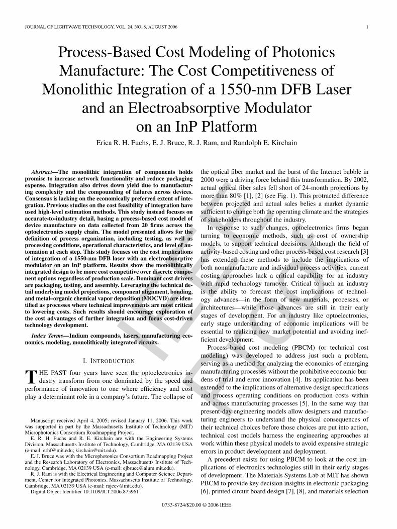
the optical fiber market and the burst of the Internet bubble in2000 were a driving force behind this transformation. By 2002,actual optical fiber sales fell short of 24-month projections bymore than 80% [1], [2] (see Fig. 1). This protracted differencebetween projected and actual sales belies a market dynamicsufficient to change both the operating climate and the strategiesof stakeholders throughout the industry.
In response to such changes, optoelectronics firms beganturning to economic methods, such as cost of ownershipmodels, to support technical decisions. Although the field ofactivity-based costing and other process-based cost research [3]has extended these methods to include the implications ofboth nonmanufacture and individual process activities, currentcosting approaches lack a critical capability for an industrywith rapid technology turnover. Critical to such an industryis the ability to forecast the cost implications of technol-ogy advances—in the form of new materials, processes, orarchitectures—while those advances are still in their earlystages of development. For an industry like optoelectronics,early stage understanding of economic implications will beessential to realizing new market potential and avoiding inef-ficient development.
Process-based cost modeling (PBCM) (or technical costmodeling) was developed to address just such a problem,serving as a method for analyzing the economics of emergingmanufacturing processes without the prohibitive economic bur-dens of trial and error innovation [4]. Its application has beenextended to the implications of alternative design specificationsand process operating conditions on production costs withinand across manufacturing processes [5]. In the same way thatpresent-day engineering models allow designers and manufac-turing engineers to understand the physical consequences oftheir technical choices before those choices are put into action,technical cost models harness the engineering approaches atwork within these physical models to avoid expensive strategicerrors in product development and deployment.
A precedent exists for using PBCM to look at the cost im-plications of electronics technologies still in their early stagesof development. The Materials Systems Lab at MIT has shownPBCM to provide key decision insights in electronic packaging[6], printed circuit board design [7], [8], and materials selection
0733-8724/$20.00 © 2006 IEEE
IEEE
Proo
f
2 JOURNAL OF LIGHTWAVE TECHNOLOGY, VOL. 24, NO. 8, AUGUST 2006
Fig. 1. Mid-2000 optical communications market forecast [1] versus actual sales [2].
for integrated circuit applications [9]–[11]. This paper has beenextended by Sandborn to look at early stage design decisionsin electronics system assembly [12], [13]. Recently, the needfor costing methods that can assess the cost implications ofemerging design alternatives has also been identified for theoptoelectronics industry. The National Electronic Manufactur-ers Initiative (NEMI) has begun a cost analysis of opticalversus copper backplanes using the PBCM approach. However,progress has been slow, and so far only a cost model of the cop-per backplane exists [14]. A yield-focused costing approach forevaluating emerging technologies also independently emergedin the late 1990s, focused on optoelectronic devices [15], [16].This approach is strongly based in theoretical yield models—calculating the yield impact of design changes on thermal dis-sipation, mechanical expansion and stress, and optical couplingefficiency [16]. This paper relies on models built around plant-level performance data, leading to different results from theseprevious theoretical analyses.
This paper presents the application of PBCM to the economicquestions associated with optoelectronic device production.The work focuses on the feasibility of a particular technologysolution—monolithic integration—for meeting the industry’sneed to drive down costs. The monolithic integration of separatecomponents on a single device not only is believed to minimizepackaging expenses but also holds promise to increase networkspeed and device functionality. However, problems arising fromincreasingly structured wafer surfaces and increased opportuni-ties for defects during the extended process flow of a monolithicdevice [17] cause concerns that yield losses will outweigh costsavings. Modeling results are used to demonstrate the impor-tance of yield losses along with several other technological andoperational characteristics of device production. The model thatis described represents a broad-scope PBCM developed as anelement of the MIT Communications Technology Roadmap-ping Project (CTR) [18] for the optoelectronics components in-dustry. This PBCM is based on data collected during a 1.5-yearperiod (September 2003 to January 2005) from 20 firms acrossthe optoelectronics supply chain located in the U.S., the U.K.,and developing East Asia. The cost results that follow are based
on the processing conditions found in the U.S.- and U.K.-basedmanufacturing facilities. The impact of manufacturing in de-veloping East Asia on the cost competitiveness of monolithi-cally integrated designs is explored in a separate paper [19].Although the model was developed around a specific InP de-vice case, the aim was to develop a model architecture easilyexpanded to address new designs, processes, and materials asmight be relevant to future questions facing the optoelectronicsindustry.
II. MODEL ARCHITECTURE
CTR PBCM allows the user to project and analyze opto-electronics production cost. The model, using basic engineeringprinciples and industry data, first estimates required processingconditions. These estimates are used to project the resourcerequirements—capital, labor, materials, and energy—needed tomeet specified production targets. These resource requirementscan be mapped to corresponding operating and investmentexpenses and then aggregated into unit cost figures as detailedsubsequently. Ultimately, the model projects the minimum ef-ficient fabrication line that is capable of producing a definedannual volume of good devices and then calculates the costof installing and operating that line. The scale of the line isdetermined by the gross devices (both acceptable and rejected)that must be processed to achieve the desired annual volume ofgood units.
The cost per good device is developed in (1)–(17). Aggregatecosts are calculated as
CTot =CMaterial + CLabor + CEnergy + CEquipment
+ CTooling + CBuilding + COverhead (1)
CEl =ACEl
PV(2)
where C represents the unit cost (per good unit), AC the annualcost (per year), PV the good devices per year, and El the costelement (materials, labor, energy, equipment, tooling, mainte-nance, and overhead).
IEEE
Proo
f
FUCHS et al.: PROCESS-BASED COST MODELING OF PHOTONICS MANUFACTURE 3
TABLE IFRONT-END PROCESS MODULES IN THE TRANSMITTER PBCM
TABLE IICLEAVING AND BACK-END PROCESS MODULES IN THE
TRANSMITTER PBCM
TABLE IIIPROCESS SUBMODEL INPUTS (REQUIRED FOR EACH PROCESS STEP)
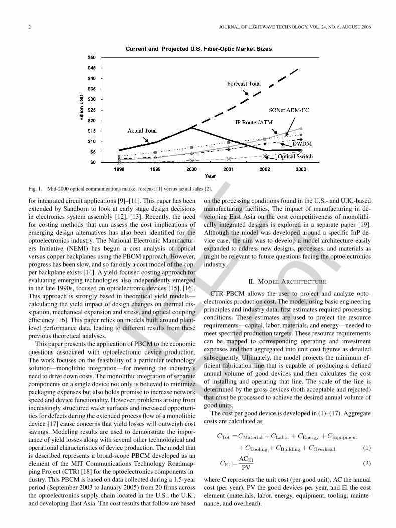
The cost projections in this paper are based on a detailed de-scription of component processing including front-end compo-nent fabrication, assembly, packaging, and all forms of testing.Model users have full flexibility to define the type and order ofprocess steps as well as set the operating conditions for eachprocess module. Currently, the model comprises 52 submodelseach covering a different process. The user identifies fromthese options both the types and order of processes requiredto produce the desired device. The 52 processes (includingtesting processes) included in the model are shown, classifiedby process function, in Tables I and II.
In defining the process flow necessary to produce a device,process type and order must by augmented by a descriptionof the materials, actions, and operating conditions occurring ata given process step. In the model, the user may choose fromone of several preset operational descriptions provided for eachprocess, or may enter his or her own recipe for the model to useat that process step. In all cases, these operational descriptionsare created from the 26 inputs shown in Table III.
A. Materials, Labor, and Energy Costs
The model currently tracks a range of materials, which areeither incorporated into the product or used as consumables(e.g., cover gases). Each process module allows the user tospecify the rate of consumption of these materials per pro-duction batch for that step. For some steps, these materialconsumption rates are forecast from descriptions of the product,but can be overridden by user input. Regarding primary waferconsumption, users may specify the density of chips that areprocessed on one wafer. Previous work has suggested there arewafer real estate benefits to system on chip solutions [20], [21].In the firms studied, the authors found wafer handling require-ments to limit the minimum chip size for the case studied inthis paper. Based on this observation, the analysis presentedassumes the same component density per wafer regardless ofwhether the component is a laser, modulator, or monolithicallyintegrated laser modulator.
Ultimately, material costs are directly driven by the effectiveproduction volume for each step (effPVi), defined as the grossnumber of units processed at step i to achieve the desirednumber of good units (PV) after step n. The calculations foreffective production volume and material costs are
effPVn = PV/Yn (3)
effPVi = effPVi+1/Yi ∀i ∈ [1, . . . , n − 1] (4)
effABi = effPVi/Batchi (5)
ACMaterial =∑i,m
Umi · effABi · Pm (6)
where i is the process step number, n is the total number ofprocess steps, Yi is the yield at step i, effABi is the gross annualbatch processed at i, Batchi is the mean batch size for i, m isthe material type, Pm is the unit price of material m, and Um
i
is the unit usage of material m per Batchi.Energy costs are based on user-specified energy consumption
rates for each machine. Energy consumption values are esti-mated for each process according to equipment requirements,leading to annual energy costs calculated as
ACEnergy =∑
i
reqLTi · EIi (7)
where EIi is the energy intensity of step i in kilowatts andreqLTi is the line time required to produce effPVi.
Users may specify direct labor requirements in four separateclassifications, namely 1) higher education labor, 2) techni-cians, 3) skilled labor, and 4) unskilled labor. The annual costof these laborers is computed as
ACLabor =∑i,l
APTli · P l (8)
where l is the labor type (Ph.D., technician, skilled, unskilled)and APTl
i is the annual paid labor time for labor type l for step i.
IEEE
Proo
f
4 JOURNAL OF LIGHTWAVE TECHNOLOGY, VOL. 24, NO. 8, AUGUST 2006
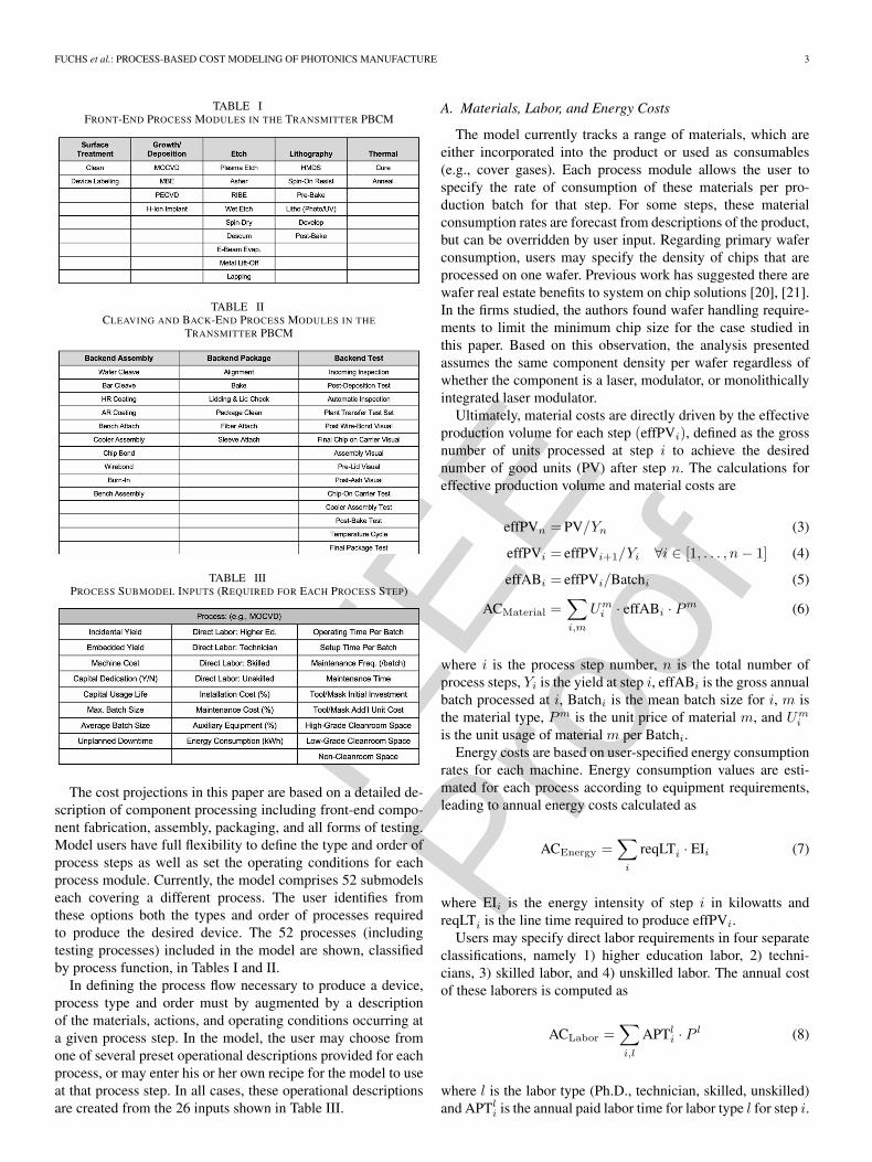
Fig. 2. Computation of available operating time based on line utilization for a 24-h day.
B. Capital Costs
A key element of any cost forecast is the method usedto allocate nonuniform cash flows to appropriate activities,here the production cost of a specific component. In the CTRPBCM, costs are assumed to be distributed evenly in time overthe usable lifetime of a resource for those cash flows withperiodicity longer than one year (e.g., equipment investments).The opportunity cost associated with tying up these funds in thislong-term investment is incorporated using a standard capitalrecovery factor [22]
REl = IEl[d(1 + d)sEl ]
[(1 + d)sEl − 1]∀ El ∈ Z (9)
where Z= {Tool, Equipment, Building}, R= the allocated costfor a defined period (here, one year), I = the nonperiodic in-vestment to be allocated, d = the periodic discount rate (here,d = 10%), s = the number of periods over which is investmentis distributed (here, sTool = 3, sEquipment = 10, and sBuilding
= 25).Along with each machine’s direct cost, an input is provided
to establish whether the machine is (a) dedicated to the produc-tion of the product being analyzed or (b) shared across otherproducts. In the latter case, following the approach of time-based allocation, investment expense is apportioned accordingto the fraction of equipment available time that is dedicated tothe manufacture of the component of interest. The details ofthis forecast are described in Section II-B1. For the purposesof the case analysis presented subsequently, the model wasconfigured based on an assumption that even if a production lineis dedicated to a single product, processes that require the sameequipment in that production line will choose, when possible,to run on the same machine. This approach was based on obser-vation of industry practice and recognition of the exceptionallylow utilization that would result otherwise for low productionvolume high-performance products. Based on this approach,fixed costs are calculated as
ACEl = ACEl,ded + ACEl,nonded
∀ El ∈ Z (10)
ACEl,nonded =∑
i
(REl,i ∗ LRi)
∀ i ∈ {nondedicated} (11)
ACEl,ded =∑
j
REl,j
(⌈∑i
(LRij−�LRij)⌉+∑
i
�LRij)
∀i ∈ {dedicated} and ∀j ∈ [1, . . . , J ] (12)
where {nondedicated} represents the set of all steps that havenondedicated processes, {dedicated} represents the set of allsteps that have dedicated processes, j is the process type, Jis the total number of process types, and LRi is the ratio ofrequired operating time to effective available operating time atstep i, as shown in the next section.
1) Operating Time: The time required for a given processstep is a key determinant of many process costs, including labor,energy, and capital requirements. Three quantities of time aretracked within any PBCM: 1) amount of time that a particularresource (machine, labor, etc.) is required—required operatingtime, 2) amount of time that a unit of that resource is availablein a given year—available operating time, and 3) amount oftime that a laborer would be paid for a full year—annual paidlabor time.
Several factors influence the required operating time, in-cluding 1) operating time per batch, 2) setup time per batch,3) machine simultaneous preparation capacity (i.e., maximumbatch size), 4) typical simultaneous preparation, 5) maintenancefrequency, and 6) maintenance duration.
The annual available operating time is required to computethe number of parallel resources necessary to meet produc-tion targets. Several operations metrics for a facility must beintegrated to compute the available operating time, includingunplanned breakdowns, worker breaks, maintenance time, andthe time when the facility is not operating (see Fig. 2). Toproperly allocate the cost of inefficient capital utilization, theavailable operating time should be modified by also subtractingthat time when the plant is operational and staffed but is notproducing due to lack of demand (i.e., idle time). This modifiedquantity, referred to as effective annual available operatingtime, is shown to the right in Fig. 2.
Annual paid labor time, lines required, required operatingtime, and available operating time are calculated as
APTli = DPY · (24 − NS − UB) · WPLl
i · LRi (13)
LRi = reqLTi/availLT (14)
reqLTi = effABi · (cycTi + suTi) (15)
availLT = DPY · (24 − NS − UB − PB − UD) (16)
where DPY represents the operating days per year, NSrepresents no operations (hours per day the plant is closed), UBrepresents the unpaid breaks (hours per day), WPLl
i representsthe fractional labor type l assigned to step i, cycTi representsthe operating cycle time of i per batch, suTi represents thesetup time of process i per batch, PB represents the paid breaks(hours per day), and UD represents the unplanned downtime(hours per day).
IEEE
Proo
f
FUCHS et al.: PROCESS-BASED COST MODELING OF PHOTONICS MANUFACTURE 5
For some processes, selected time quantities are not userinputs, but instead are computed based on descriptions of theproduct or desired operating conditions. For example, set uptime can be correlated to the extent of automation of themachine and operating time per batch can be modeled fromprocessing or product requirements such as thickness deposited,number of wires in wire bond, or type of epoxy and temperatureof oven.2) Yield: The unit costs (CTot) reported in this paper rep-
resent what is often known in the industry as “yielded costs,”in other words the effective cost per good nondefective device.Unlike classic industry models, two yield numbers are assignedto each step in the process flow—an incidental yield and anembedded yield. Both of these yield values are inputs providedfor each step by the user. The incidental yield represents theyield hit taken immediately at a given step due to obviousproblems that can be identified without testing (e.g., occasionalwafer breakage). The embedded yield represents defects causedwithin a process step but not discarded from the production lineuntil later when identified as defective during testing. Thus,embedded yields accumulate during production until they areidentified and removed during a testing step. Although onlyprocess steps that are not test steps can have embedded yields,test steps may have their own incidental yield. Equation (17)shows how yield (Yi) would be calculated for some step i = k,where k ∈ [0, . . . , n], i.e.,
Yi=k =
incYk ·
k∏x=(t∗+1)
embYx, k = test
incYk, k = test
(17)
where t∗ = max�, ∀i ∈ {test}, where � = {i}k−1i=1 and {test}
represents the set of steps that are test steps. In words, t∗ is themost recent step prior to k that was a test. The user inputsincidental yield (incYi) and embedded yield (embYi) for all i.Assuming a total of n steps in the process flow, the cumulativeyield YCumulative can be calculated as
YCumulative =n∏
i=1
Yi. (18)
The yields (Yi) used for the analysis presented in this paper arebased on the yields the studied firms were able to achieve post-rework. Future modeling efforts to integrate the direct cost ofrework would be a useful extension of this analysis.
III. CASE STUDY
The main goal of this study has been to develop a modelwhose architecture will become the foundation for investigatingfuture techno-economic questions facing the optoelectronicsindustry. Particularly important is for the model to provideinsights on the cost feasibility of integrating separate compo-nents on a single device. Limits of time and resources requiredchoosing a single case from which future studies and modeldevelopments could be built. Three attributes are particularlyimportant in the case chosen for study, namely 1) the case pro-vides insights on a large range of processes necessary in opto-
TABLE IVEXOGENOUS FINANCIAL PARAMETERS USED IN CASE STUDY ANALYSES
electronic chip production, 2) the case focuses on emerging butextant technology for which significant data are available withinthe industry (i.e., from which to develop models of relevantprocesses and against which model results can be calibrated),and 3) the case addresses a key integration decision being facedby firms. In light of these criteria, production of a 1550-nmDFB laser and an electroabsorptive modulator on an InP plat-form was chosen as the case for study. This laser modulatoris designed for use in long- and short-haul STM-64/OC-192time-division multiplexing applications over 40, 60, and80 km with low dispersion penalty (less than 2 dB). Such alaser modulator would be suitable for use in SONET and SDH(∼ 9.953 Gb/s), and as a Digital Wrapper (∼ 10.3 Gb/s), withFEC (∼ 10.7 Gb/s) (Table IV).
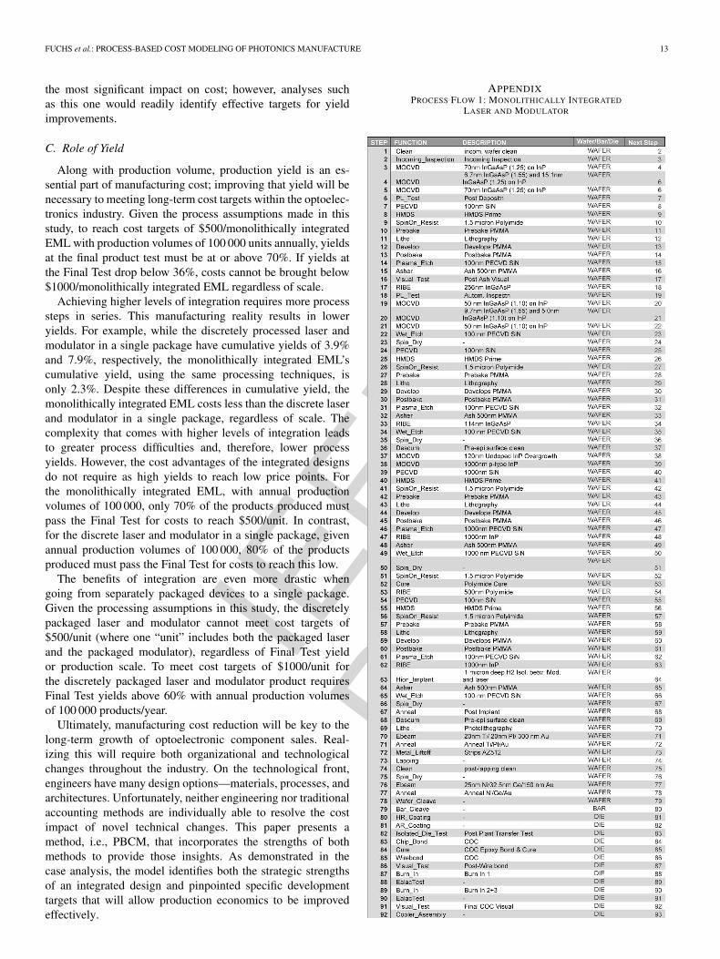
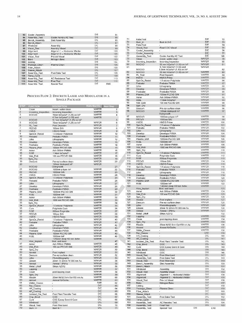
Three scenarios around this case were investigated, namely1) a discretely packaged 1550-nm InP DFB laser and a dis-cretely packaged electroabsorptive modulator, 2) a discrete1550-nm InP DFB laser and a discrete electroabsorptive mod-ulator within a single package, and 3) a 1550-nm InP DFBlaser and an electroabsorptive modulator monolithically inte-grated on a single device. The 182-step, 165-step, and 111-stepprocess flows for production of the 1) discretely packaged laserand discretely packaged modulator designs, 2) discrete laserand modulator in a single package, and 3) monolithically inte-grated are shown at the end of the document. All three scenariosare intended to represent the production of functionally equiv-alent 10-Gb/s devices with stringent quality specifications. Allthree product scenarios were modeled using a common set ofoperational and financial conditions as listed in Tables I and II.
Data for both the processes and the process flows relevant tothese cases were collected from 20 firms across the optoelec-tronics supply chain, including end users, original equipmentmanufacturers (OEMs), and equipment manufacturers. Thesedata were aggregated to construct a scenario illustrative of gen-eral industry practice. The process flow and process informationfor case 1 (discrete devices in discrete packages) was derivedbased on information collected about case 2 (discrete devices ina single package). As such, it likely represents an upper boundof cost and a lower bound of yield for case 1.
IEEE
Proo
f
6 JOURNAL OF LIGHTWAVE TECHNOLOGY, VOL. 24, NO. 8, AUGUST 2006
Fig. 3. Cost sensitivity of production volume analysis to final product yield. (For this analysis, the yield Yn of the final step was varied to create the cumulativeyields YCumulative reported. In both of these process flows, the final step is a test.)
The following section details the use of CTR PBCM to mapthe technological and strategic characteristics of the tradeoffbetween packaging gains and processing losses for discreteand integrated designs of a 1550-nm DFB laser and an elec-troabsorptive modulator realized on an InP platform. Particu-lar focus is paid to three economic aspects of this problem,namely 1) quantifying the impact of production scale growth,2) identifying cost drivers, and 3) quantifying process perfor-mance levels necessary to achieve production cost targets.
A. Quantifying the Impact of Production Scale Growth
A critical economic characteristic of any technology is themanner in which its production costs change as a function oftotal units produced. A PBCM forecasts this change in produc-tion costs with scale by first determining the minimum efficientfabrication line that is capable of producing a given quantity ofgood devices and then inferring the cost of operating that line.Fig. 3 shows such an analysis for the laser modulator designoptions. To generate these results, the model projects technicaland operational characteristics of the smallest efficient fabrica-tion and assembly facility capable of meeting the productionvolume (of good devices) enumerated along the x-axis.
The reported cost figures represent the operating andallocated capital expenses associated with that facility andthe product of interest. All three design options, namely1) a discretely packaged 1550-nm InP laser and a discretelypackaged modulator (discrete package), 2) a discrete laser anda discrete modulator within a single package (discrete device),and 3) a monolithically integrated 1550-nm InP laser modulator(monolithically integrated), showed strong economies of scaleup to annual production volumes of approximately 30 000units. At annual volumes above 30 000 units, the productioncosts of all three devices become effectively insensitiveto production scale. The unit cost of the monolithicallyintegrated electroabsorptive modulated laser (EML) levels
TABLE VLARGEST CONTRIBUTORS TO INVESTMENT FOR EACH DESIGN AT
ANNUAL PRODUCTION VOLUMES OF 30 000 ANNUALLY
out at just above $500 per unit, the discretely produceddevices within a single package level out at a cost just below$600 per unit, and the discretely packaged devices level out ata cost of around $850 per unit. The discrete device case (i.e.,within a single package) showed the strongest sensitivity toscale, followed by production of discretely packaged devices.This relative behavior emerges because both discrete productsrequire larger total investments compared to the monolithicallyintegrated design. The monolithically integrated EML requiresthe least investment and therefore shows the least sensitivityto scale. The largest contributors to investment cost for eachdevice can be seen in Table V. Because the discretely packageddevices were found to be cost inferior to the other two optionsat all production volumes, this scenario is left out of theanalyses for the rest of this paper.
It may seem surprising that the model would project a smallercapital outlay (and corresponding less volume-sensitive unitcost) for the monolithic device despite its overall lowerproduction yield; lower yield products require more units to be
IEEE
Proo
f
FUCHS et al.: PROCESS-BASED COST MODELING OF PHOTONICS MANUFACTURE 7
Fig. 4. Monolithically integrated laser-modulator device cost breakdown at 30 000 units annually.
processed that in turn drives higher equipment requirements.While the model does project that production of the monolithicdevice requires higher capital utilization than its discrete devicecounterparts, in all three cases, production requirements canusually be satisfied by a single piece of equipment across therange of production volumes being considered. As such, formany processing steps, the yield disadvantage of the monolithicdevice is insufficient to drive additional capital expenditure.However, there are a few processing steps that both have longcycle times (i.e., require multiple units of equipment) and mustbe repeated for each discrete component. Excellent examplesof this are chip bonding and its associated testing operations. Inthese cases, the additional required instances of these processesin the discrete cases lead to additional capital requirements andthe observed cost behavior.
Both the volume at which economies of scale are reached andthe eventual cost at scale are dependent on the specific process-ing decisions and conditions faced by an individual plant. In theanalysis shown in Fig. 3, testing occurs after six key intervalsfor the front end, after individual die isolation (bar cleave), andat five key locations during the back end processes (see Appen-dix, for specific locations). The final product yields achievedare 2.3% for the monolithically integrated device, and 3.9%and 7.9% for the discrete laser and modulator, respectively,in a single package. Because data for the discretely packageddevices are derived directly from information collected oncase 2, the yields for this case match those of the discrete-device single-package case.
With yields in single digits, even slight improvements ordigressions within individual process steps can have significantconsequences. The impact of small yield changes on the finalproduct cost can be seen for the monolithic and discrete devicecases as the shaded areas in Fig. 3. The dominance of one caseover the other is susceptible to the yields producers are actuallyable to achieve.
B. Identifying Cost Drivers
Although knowing the costs of alternative scenarios and howthese costs vary with production scale is useful for strategic
decision making, more detailed information is required forinformed operational decisions and firm-wide efforts to reducecost. PBCM addresses this issue by providing the user with awide variety of scenarios under which to observe the dominantdrivers of production cost. Knowledge of cost drivers enablesthe industry to focus scarce development resources on thesedominant areas. The next five figures demonstrate the insightsthe CTR PBCM provides on the cost drivers in 1550-nm InPlaser modulator production.
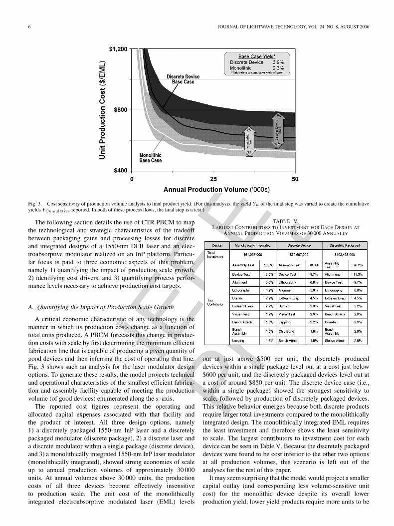
Fig. 4 provides an aggregate breakdown of costs for themonolithically integrated device at a production volume of30 000 units per year. In this and the four subsequent figures,costs are grouped into four headings, namely 1) materials(including purchased packaging components), 2) labor (directand indirect, both with benefits, but not managerial costs);3) energy, and 4) equipment, and other fixed (comprising ofbuilding, maintenance, and overhead, with overhead includingmanagerial overhead costs). For the monolithically integratedcase, equipment represents the largest cost, accounting fornearly 37% of the total at this production volume. Equipmentcosts are followed by materials, which comprise almost 27% ofthe total cost.
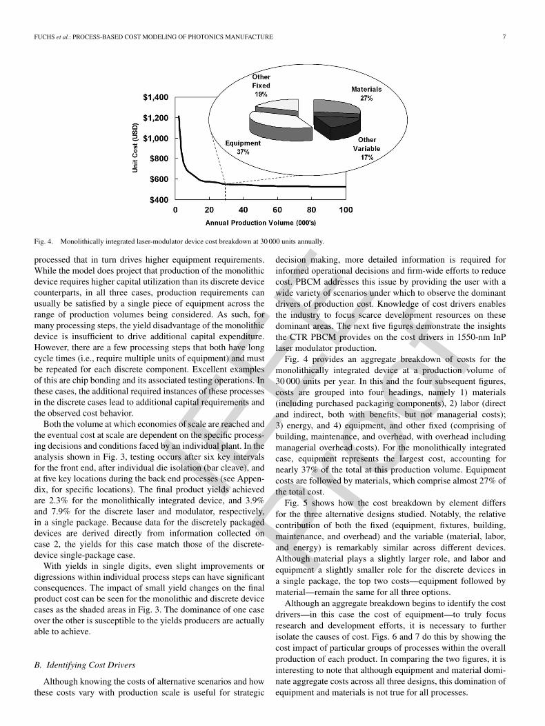
Fig. 5 shows how the cost breakdown by element differsfor the three alternative designs studied. Notably, the relativecontribution of both the fixed (equipment, fixtures, building,maintenance, and overhead) and the variable (material, labor,and energy) is remarkably similar across different devices.Although material plays a slightly larger role, and labor andequipment a slightly smaller role for the discrete devices ina single package, the top two costs—equipment followed bymaterial—remain the same for all three options.
Although an aggregate breakdown begins to identify the costdrivers—in this case the cost of equipment—to truly focusresearch and development efforts, it is necessary to furtherisolate the causes of cost. Figs. 6 and 7 do this by showing thecost impact of particular groups of processes within the overallproduction of each product. In comparing the two figures, it isinteresting to note that although equipment and material domi-nate aggregate costs across all three designs, this domination ofequipment and materials is not true for all processes.
IEEE
Proo
f
8 JOURNAL OF LIGHTWAVE TECHNOLOGY, VOL. 24, NO. 8, AUGUST 2006
Fig. 5. Cost breakdown comparison at 30 000 units annually for different levels of integration.
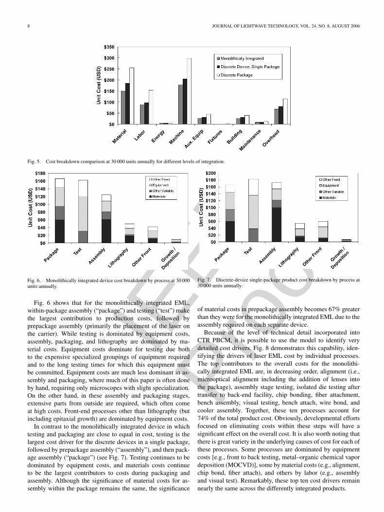
Fig. 6. Monolithically integrated device cost breakdown by process at 30 000units annually.
Fig. 6 shows that for the monolithically integrated EML,within-package assembly (“package”) and testing (“test”) makethe largest contribution to production costs, followed byprepackage assembly (primarily the placement of the laser onthe carrier). While testing is dominated by equipment costs,assembly, packaging, and lithography are dominated by ma-terial costs. Equipment costs dominate for testing due bothto the expensive specialized groupings of equipment requiredand to the long testing times for which this equipment mustbe committed. Equipment costs are much less dominant in as-sembly and packaging, where much of this paper is often doneby hand, requiring only microscopes with slight specialization.On the other hand, in these assembly and packaging stages,extensive parts from outside are required, which often comeat high costs. Front-end processes other than lithography (butincluding epitaxial growth) are dominated by equipment costs.
In contrast to the monolithically integrated device in whichtesting and packaging are close to equal in cost, testing is thelargest cost driver for the discrete devices in a single package,followed by prepackage assembly (“assembly”), and then pack-age assembly (“package”) (see Fig. 7). Testing continues to bedominated by equipment costs, and materials costs continueto be the largest contributors to costs during packaging andassembly. Although the significance of material costs for as-sembly within the package remains the same, the significance
Fig. 7. Discrete-device single-package product cost breakdown by process at30 000 units annually.
of material costs in prepackage assembly becomes 67% greaterthan they were for the monolithically integrated EML due to theassembly required on each separate device.
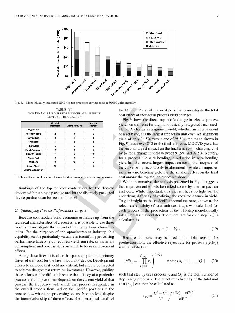
Because of the level of technical detail incorporated intoCTR PBCM, it is possible to use the model to identify verydetailed cost drivers. Fig. 8 demonstrates this capability, iden-tifying the drivers of laser EML cost by individual processes.The top contributors to the overall costs for the monolithi-cally integrated EML are, in decreasing order, alignment (i.e.,microoptical alignment including the addition of lenses intothe package), assembly stage testing, isolated die testing aftertransfer to back-end facility, chip bonding, fiber attachment,bench assembly, visual testing, bench attach, wire bond, andcooler assembly. Together, these ten processes account for74% of the total product cost. Obviously, developmental effortsfocused on eliminating costs within these steps will have asignificant effect on the overall cost. It is also worth noting thatthere is great variety in the underlying causes of cost for each ofthese processes. Some processes are dominated by equipmentcosts [e.g., front to back testing, metal–organic chemical vapordeposition (MOCVD)], some by material costs (e.g., alignment,chip bond, fiber attach), and others by labor (e.g., assemblyand visual test). Remarkably, these top ten cost drivers remainnearly the same across the differently integrated products.
IEEE
Proo
f
FUCHS et al.: PROCESS-BASED COST MODELING OF PHOTONICS MANUFACTURE 9
Fig. 8. Monolithically integrated EML top ten processes driving costs at 30 000 units annually.
TABLE VITOP TEN COST DRIVERS FOR DEVICES AT DIFFERENT
LEVELS OF INTEGRATION
Rankings of the top ten cost contributors for the discretedevices within a single package and for the discretely packageddevice products can be seen in Table VI.
C. Quantifying Process Performance Targets
Because cost models build economic estimates up from thetechnical characteristics of a process, it is possible to use thesemodels to investigate the impact of changing those character-istics. For the purposes of the optoelectronics industry, thiscapability can be particularly valuable in identifying processingperformance targets (e.g., required yield, run rate, or materialsconsumption) and process steps on which to focus improvementefforts.
Along these lines, it is clear that per step yield is a primarydriver of unit cost for the laser modulator device. Developmentefforts to improve that yield are critical, but should be targetedto achieve the greatest return on investment. However, guidingthese efforts can be difficult because the efficacy of a particularprocess yield improvement depends on the current yield of thatprocess, the frequency with which that process is repeated inthe overall process flow, and on the specific positions in theprocess flow where that processing occurs. Nonetheless, despitethe interrelationship of these effects, the operational detail of
the MIT CTR model makes it possible to investigate the totalcost effect of individual process yield changes.
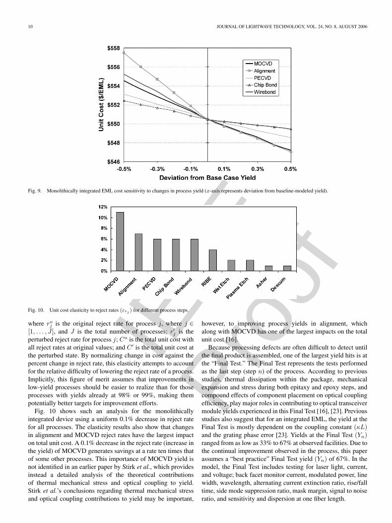
Fig. 9 shows the direct impact of a change in selected processyields on unit cost for the monolithically integrated laser mod-ulator. A change in alignment yield, whether an improvementor a set back, has the largest impact on unit cost. An alignmentyield of only 94.5% versus one of 95.5% (the range shown inFig. 9) adds over $10 to the final unit cost. MOCVD yield hasthe second largest impact on the final unit cost—changing costby $7 for a change in yield between 91.5% and 92.5%. Notably,for a process like wire bonding, a reduction in wire bondingyield has the second largest impact on cost—the steepness ofthe curve being second only to alignment—while an improve-ment in wire bonding yield has the smallest effect on the finalcost among the top ten the processes shown.
While informative, the analysis presented in Fig. 9 suggeststhat improvement efforts be ranked solely by their impact onunit cost. While important, this metric sheds no light on theunderlying difficulty of realizing the required change in yield.To gain insight on this tradeoff, a second measure, known as thereject rate elasticity of total unit cost (εrj
), was calculated foreach process in the production of the 111-step monolithicallyintegrated laser modulator. The reject rate for each step (ri) iscalculated as
ri = (1 − Yi). (19)
Because a process may be used at multiple steps in theproduction flow, the effective reject rate for process j(effrj)was calculated as
effrj =
Qj∏
q=1
rq
1/Qj
∀ steps qj ∈ [1, . . . , Qj ] (20)
such that step qj uses process j, and Qj is the total number ofsteps using process j. The reject rate elasticity of the total unitcost (εrj
) can then be calculated as
εrj=
C ′ − Co
Co
/effr′j − effro
j
effroj
(21)
IEEE
Proo
f
10 JOURNAL OF LIGHTWAVE TECHNOLOGY, VOL. 24, NO. 8, AUGUST 2006
Fig. 9. Monolithically integrated EML cost sensitivity to changes in process yield (x-axis represents deviation from baseline-modeled yield).
Fig. 10. Unit cost elasticity to reject rates (εrj ) for different process steps.
where roj is the original reject rate for process j, where j ∈
[1, . . . , J ], and J is the total number of processes; r′j is theperturbed reject rate for process j; Co is the total unit cost withall reject rates at original values; and C ′ is the total unit cost atthe perturbed state. By normalizing change in cost against thepercent change in reject rate, this elasticity attempts to accountfor the relative difficulty of lowering the reject rate of a process.Implicitly, this figure of merit assumes that improvements inlow-yield processes should be easier to realize than for thoseprocesses with yields already at 98% or 99%, making thempotentially better targets for improvement efforts.
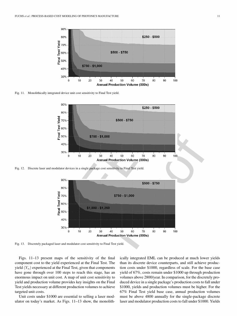
Fig. 10 shows such an analysis for the monolithicallyintegrated device using a uniform 0.1% decrease in reject ratefor all processes. The elasticity results also show that changesin alignment and MOCVD reject rates have the largest impacton total unit cost. A 0.1% decrease in the reject rate (increase inthe yield) of MOCVD generates savings at a rate ten times thatof some other processes. This importance of MOCVD yield isnot identified in an earlier paper by Stirk et al., which providesinstead a detailed analysis of the theoretical contributionsof thermal mechanical stress and optical coupling to yield.Stirk et al.’s conclusions regarding thermal mechanical stressand optical coupling contributions to yield may be important,
however, to improving process yields in alignment, whichalong with MOCVD has one of the largest impacts on the totalunit cost [16].
Because processing defects are often difficult to detect untilthe final product is assembled, one of the largest yield hits is atthe “Final Test.” The Final Test represents the tests performedas the last step (step n) of the process. According to previousstudies, thermal dissipation within the package, mechanicalexpansion and stress during both epitaxy and epoxy steps, andcompound effects of component placement on optical couplingefficiency, play major roles in contributing to optical transceivermodule yields experienced in this Final Test [16], [23]. Previousstudies also suggest that for an integrated EML, the yield at theFinal Test is mostly dependent on the coupling constant (κL)and the grating phase error [23]. Yields at the Final Test (Yn)ranged from as low as 33% to 67% at observed facilities. Due tothe continual improvement observed in the process, this paperassumes a “best practice” Final Test yield (Yn) of 67%. In themodel, the Final Test includes testing for laser light, current,and voltage; back facet monitor current, modulated power, linewidth, wavelength, alternating current extinction ratio, rise/falltime, side mode suppression ratio, mask margin, signal to noiseratio, and sensitivity and dispersion at one fiber length.
IEEE
Proo
f
FUCHS et al.: PROCESS-BASED COST MODELING OF PHOTONICS MANUFACTURE 11
Fig. 11. Monolithically integrated device unit cost sensitivity to Final Test yield.
Fig. 12. Discrete laser and modulator devices in a single package cost sensitivity to Final Test yield.
Fig. 13. Discretely packaged laser and modulator cost sensitivity to Final Test yield.
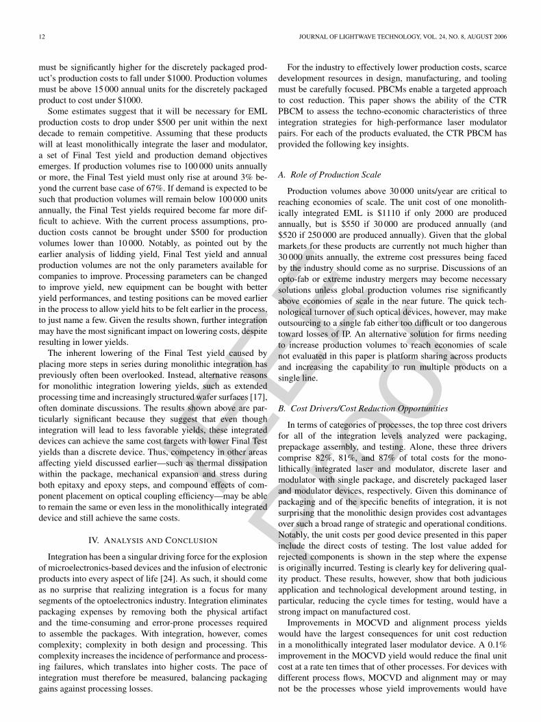
Figs. 11–13 present maps of the sensitivity of the finalcomponent cost to the yield experienced at the Final Test. Theyield (Yn) experienced at the Final Test, given that componentshave gone through over 100 steps to reach this stage, has anenormous impact on unit cost. A map of unit cost sensitivity toyield and production volume provides key insights on the FinalTest yields necessary at different production volumes to achievetargeted unit costs.
Unit costs under $1000 are essential to selling a laser mod-ulator on today’s market. As Figs. 11–13 show, the monolith-
ically integrated EML can be produced at much lower yieldsthan its discrete device counterparts, and still achieve produc-tion costs under $1000, regardless of scale. For the base caseyield of 67%, costs remain under $1000 up through productionvolumes above 2800/year. In comparison, for the discretely pro-duced device in a single package’s production costs to fall under$1000, yields and production volumes must be higher. For the67% Final Test yield base case, annual production volumesmust be above 4800 annually for the single-package discretelaser and modulator production costs to fall under $1000. Yields
IEEE
Proo
f
12 JOURNAL OF LIGHTWAVE TECHNOLOGY, VOL. 24, NO. 8, AUGUST 2006
must be significantly higher for the discretely packaged prod-uct’s production costs to fall under $1000. Production volumesmust be above 15 000 annual units for the discretely packagedproduct to cost under $1000.
Some estimates suggest that it will be necessary for EMLproduction costs to drop under $500 per unit within the nextdecade to remain competitive. Assuming that these productswill at least monolithically integrate the laser and modulator,a set of Final Test yield and production demand objectivesemerges. If production volumes rise to 100 000 units annuallyor more, the Final Test yield must only rise at around 3% be-yond the current base case of 67%. If demand is expected to besuch that production volumes will remain below 100 000 unitsannually, the Final Test yields required become far more dif-ficult to achieve. With the current process assumptions, pro-duction costs cannot be brought under $500 for productionvolumes lower than 10 000. Notably, as pointed out by theearlier analysis of lidding yield, Final Test yield and annualproduction volumes are not the only parameters available forcompanies to improve. Processing parameters can be changedto improve yield, new equipment can be bought with betteryield performances, and testing positions can be moved earlierin the process to allow yield hits to be felt earlier in the process,to just name a few. Given the results shown, further integrationmay have the most significant impact on lowering costs, despiteresulting in lower yields.
The inherent lowering of the Final Test yield caused byplacing more steps in series during monolithic integration haspreviously often been overlooked. Instead, alternative reasonsfor monolithic integration lowering yields, such as extendedprocessing time and increasingly structured wafer surfaces [17],often dominate discussions. The results shown above are par-ticularly significant because they suggest that even thoughintegration will lead to less favorable yields, these integrateddevices can achieve the same cost targets with lower Final Testyields than a discrete device. Thus, competency in other areasaffecting yield discussed earlier—such as thermal dissipationwithin the package, mechanical expansion and stress duringboth epitaxy and epoxy steps, and compound effects of com-ponent placement on optical coupling efficiency—may be ableto remain the same or even less in the monolithically integrateddevice and still achieve the same costs.
IV. ANALYSIS AND CONCLUSION
Integration has been a singular driving force for the explosionof microelectronics-based devices and the infusion of electronicproducts into every aspect of life [24]. As such, it should comeas no surprise that realizing integration is a focus for manysegments of the optoelectronics industry. Integration eliminatespackaging expenses by removing both the physical artifactand the time-consuming and error-prone processes requiredto assemble the packages. With integration, however, comescomplexity; complexity in both design and processing. Thiscomplexity increases the incidence of performance and process-ing failures, which translates into higher costs. The pace ofintegration must therefore be measured, balancing packaginggains against processing losses.
For the industry to effectively lower production costs, scarcedevelopment resources in design, manufacturing, and toolingmust be carefully focused. PBCMs enable a targeted approachto cost reduction. This paper shows the ability of the CTRPBCM to assess the techno-economic characteristics of threeintegration strategies for high-performance laser modulatorpairs. For each of the products evaluated, the CTR PBCM hasprovided the following key insights.
A. Role of Production Scale
Production volumes above 30 000 units/year are critical toreaching economies of scale. The unit cost of one monolith-ically integrated EML is $1110 if only 2000 are producedannually, but is $550 if 30 000 are produced annually (and$520 if 250 000 are produced annually). Given that the globalmarkets for these products are currently not much higher than30 000 units annually, the extreme cost pressures being facedby the industry should come as no surprise. Discussions of anopto-fab or extreme industry mergers may become necessarysolutions unless global production volumes rise significantlyabove economies of scale in the near future. The quick tech-nological turnover of such optical devices, however, may makeoutsourcing to a single fab either too difficult or too dangeroustoward losses of IP. An alternative solution for firms needingto increase production volumes to reach economies of scalenot evaluated in this paper is platform sharing across productsand increasing the capability to run multiple products on asingle line.
B. Cost Drivers/Cost Reduction Opportunities
In terms of categories of processes, the top three cost driversfor all of the integration levels analyzed were packaging,prepackage assembly, and testing. Alone, these three driverscomprise 82%, 81%, and 87% of total costs for the mono-lithically integrated laser and modulator, discrete laser andmodulator with single package, and discretely packaged laserand modulator devices, respectively. Given this dominance ofpackaging and of the specific benefits of integration, it is notsurprising that the monolithic design provides cost advantagesover such a broad range of strategic and operational conditions.Notably, the unit costs per good device presented in this paperinclude the direct costs of testing. The lost value added forrejected components is shown in the step where the expenseis originally incurred. Testing is clearly key for delivering qual-ity product. These results, however, show that both judiciousapplication and technological development around testing, inparticular, reducing the cycle times for testing, would have astrong impact on manufactured cost.
Improvements in MOCVD and alignment process yieldswould have the largest consequences for unit cost reductionin a monolithically integrated laser modulator device. A 0.1%improvement in the MOCVD yield would reduce the final unitcost at a rate ten times that of other processes. For devices withdifferent process flows, MOCVD and alignment may or maynot be the processes whose yield improvements would have
IEEE
Proo
f
FUCHS et al.: PROCESS-BASED COST MODELING OF PHOTONICS MANUFACTURE 13
the most significant impact on cost; however, analyses suchas this one would readily identify effective targets for yieldimprovements.
C. Role of Yield
Along with production volume, production yield is an es-sential part of manufacturing cost; improving that yield will benecessary to meeting long-term cost targets within the optoelec-tronics industry. Given the process assumptions made in thisstudy, to reach cost targets of $500/monolithically integratedEML with production volumes of 100 000 units annually, yieldsat the final product test must be at or above 70%. If yields atthe Final Test drop below 36%, costs cannot be brought below$1000/monolithically integrated EML regardless of scale.
Achieving higher levels of integration requires more processsteps in series. This manufacturing reality results in loweryields. For example, while the discretely processed laser andmodulator in a single package have cumulative yields of 3.9%and 7.9%, respectively, the monolithically integrated EML’scumulative yield, using the same processing techniques, isonly 2.3%. Despite these differences in cumulative yield, themonolithically integrated EML costs less than the discrete laserand modulator in a single package, regardless of scale. Thecomplexity that comes with higher levels of integration leadsto greater process difficulties and, therefore, lower processyields. However, the cost advantages of the integrated designsdo not require as high yields to reach low price points. Forthe monolithically integrated EML, with annual productionvolumes of 100 000, only 70% of the products produced mustpass the Final Test for costs to reach $500/unit. In contrast,for the discrete laser and modulator in a single package, givenannual production volumes of 100 000, 80% of the productsproduced must pass the Final Test for costs to reach this low.
The benefits of integration are even more drastic whengoing from separately packaged devices to a single package.Given the processing assumptions in this study, the discretelypackaged laser and modulator cannot meet cost targets of$500/unit (where one “unit” includes both the packaged laserand the packaged modulator), regardless of Final Test yieldor production scale. To meet cost targets of $1000/unit forthe discretely packaged laser and modulator product requiresFinal Test yields above 60% with annual production volumesof 100 000 products/year.
Ultimately, manufacturing cost reduction will be key to thelong-term growth of optoelectronic component sales. Real-izing this will require both organizational and technologicalchanges throughout the industry. On the technological front,engineers have many design options—materials, processes, andarchitectures. Unfortunately, neither engineering nor traditionalaccounting methods are individually able to resolve the costimpact of novel technical changes. This paper presents amethod, i.e., PBCM, that incorporates the strengths of bothmethods to provide those insights. As demonstrated in thecase analysis, the model identifies both the strategic strengthsof an integrated design and pinpointed specific developmenttargets that will allow production economics to be improvedeffectively.
APPENDIXPROCESS FLOW 1: MONOLITHICALLY INTEGRATED
LASER AND MODULATOR
IEEE
Proo
f
14 JOURNAL OF LIGHTWAVE TECHNOLOGY, VOL. 24, NO. 8, AUGUST 2006
PROCESS FLOW 2: DISCRETE LASER AND MODULATOR IN A
SINGLE PACKAGE
IEEE
Proo
f
FUCHS et al.: PROCESS-BASED COST MODELING OF PHOTONICS MANUFACTURE 15
REFERENCES
[1] “Miconex 2000 Continues Growing: Current and projected U.S. fiberoptic market sizes,” in Control Eng., vol. 47, Dec. 1, 2000, p. 12. ReedBusiness Information.
[2] L. Turbini and J. Stafford, “NEMI optoelectronics technology roadmap,”in Optoelectron. Microsys. Int. (OMI) Conf., Apr. 30, 2003.
[3] C. Bloch and R. Ranganathan, “Process-based cost modeling,” IEEETrans. Compon., Hybrids, Manuf. Technol., vol. 15, no. 3, pp. 288–294,Jun. 1992.
[4] J. V. Busch and F. R. Field, “Technical cost modeling,” in The BlowMolding Handbook, D. Rosato and D. Rosato, Eds. New York: Hansr,1988.
[5] R. Kirchain and F. Field, “Process-based cost modeling: Understand-ing the economics of technical decisions,” in Encyclopedia of MaterialsScience and Engineering. Oxford, U.K.: Elsevier, 2000.
[6] S. Sikorski, R. Krueger, and F. Field, “A systems approach to the eval-uation of packaging design alternatives,” Int. J. Hybrid Microelectron.,vol. 12, no. 1, 1989.
[7] F. Field and L. Ng, “Materials for printed circuit boards: Past usage andfuture prospects,” Mater. Soc., vol. 13, no. 3, pp. 301–318, Jan. 1989.
[8] ——, “Technical cost modeling for printed circuit board fabrication,”Print. Circuit Fabr., vol. 12, no. 2, Mar. 1989.
[9] J. Dieffenbach and S. Marallo, “Large area thin film multichip modules:The impact of learning curve improvements on manufacturing cost,” inProc. SEMICON WEST: Critical Packag. Technol. ’90s, Jul. 1994.
[10] L. Ng, “What drives the cost of thin film multichip modules?” in Proc.Jpn. Int. Electron. Manuf. Technol. Symp., Tokyo, Japan, 1991.
[11] J. Dieffenbach, “Multichip module technology development: Lessonslearned from cost modeling,” in Mater. Sci. Eng.. Cambridge, MA:Mass. Inst. Technol., 1989.
[12] P. A. Sandborn, “Analyzing packaging trade-offs during system design,”IEEE Des. Test Comput., vol. 15, no. 3, Jul./Sep. 1998.
[13] T. Trichy, P. Sandborn, R. Raghavan, and S. Sahasrabudhe, “A newtest/diagnosis/rework model for use in technical cost modeling of elec-tronic systems assembly,” in Proc. Int. Test Conf., 2001, pp. 1108–1117.
[14] A. Singer, “NEMI cost analysis: Optical versus copper backplanes,” inAPEX: Shared Intelligence (TM), 2004.
[15] C. Stirk, Q. Liu, and M. Ball, “Manufacturing cost analysis of inte-grated photonic packages,” in Proc. SPIE Conf. Photon. Packag. Integr.San Jose, CA: SPIE, 1999.
[16] C. Stirk, N. Delen, A. Fedor, M. Ball, R. B. Hooker, J. S. Wu, S. Hareb,T. H. Ju, and Y. C. Lee, “Cost, performance, and reliability simulator foroptical transceiver modules,” Appl. Opt., vol. 37, no. 26, pp. 6151–6160,Sep. 1998.
[17] R. Maerz, H. F. Mahlein, and B. Acklin, “Yield and cost model forintegrated optical chips,” J. Lightw. Technol., vol. 14, no. 2, pp. 158–163,Feb. 1996.
[18] E. Bruce and C. Fine, “Technology roadmapping: Mapping a future forintegrated photonics,” J. Lightw. Technol., 2005. Invited Tutorial, to bepublished.
[19] E. Fuchs and R. Kirchain, “Changing paths: The impact of manufactur-ing location on technology development incentives in the optoelectronicsindustry,” in Proc. Annu. Academy Manag. Conf., Honolulu, HI, 2005,p. 1335.
[20] M. Shen, L. Zheng, and H. Tenhunen, “Cost and performance analy-sis for mixed-signal system implementation: System-on-chip or system-on-package?” IEEE Trans. Electron. Packag. Manuf., vol. 25, no. 4,pp. 262–272, Oct. 2002.
[21] L. Zheng, X. Duo, S. Meigen, W. Michielsen, and H. Tenhunen, “Costand performance tradeoff analysis in radio and mixed-signal system-on-package design,” IEEE Trans. Adv. Packag., vol. 27, no. 2, pp. 364–375,May 2004.
[22] R. de Neufville, Applied Systems Analysis: Engineering Planning andTechnology Management. New York: McGraw-Hill, 1990, p. 207.
[23] Y. Kim, S. Nam, and J. Jeong, “Yield estimation of 10 Gb/s electroab-sorption modulator-integrated DFB lasers due to chirp,” IEEE Photon.Technol. Lett., vol. 14, no. 4, pp. 447–449, Apr. 2002.
[24] L. C. Kimerling, “Photons to the rescue: Microelectronics becomesmicrophotonics,” Interface, vol. 9, no. 2, pp. 28–31, 2000.
Erica R. H. Fuchs was born in Reading, PA. She received the S.B. degreein materials science and engineering from the Massachusetts Institute ofTechnology (MIT), Cambridge, in 1999, the S.M. degree in technology andpolicy, MIT in 2002, and the Ph.D. degree in engineering systems from MITin 2006.
She is currently a Post Doctoral Fellow at the Materials Processing Centerat MIT. She is the coauthor of “Changing Paths: The Impact of Manufactur-ing Off-Shore on Technology Development Incentives in the OptoelectronicsIndustry” (2005 Annual Meeting of the Academy of Management, Aug. 5–10,Honolulu, HI) and “The Future of the Asian Auto Industry: Regional Integra-tion, Alternative Designs, and Chinese Leadership” (International Journal ofVehicle Design, 2002). Her research focuses on materials selection, the costcompetitiveness of emerging technologies, and the impact of manufacturinglocation on the industries’ long-term technology development paths.
E. J. Bruce received the B.S. degree in electrical engineering with a spe-cialization in photonics from the University of Washington, Seattle, in 1994and the M.E. degree from the Massachusetts Institute of Technology (MIT),Cambridge, in 1998.
She recently served as a Strategic Project Manager with the TechnologyStrategy group, Analog Devices, Inc. She was also an Associate Director withthe Center for Integrated Photonic Systems, MIT, where she played a leadingrole in the Communication Technology Road mapping program for three years.Prior to joining MIT, she was a Senior Analyst with the Aberdeen Group, amarket research and consulting firm based in Boston, MA. In addition, shehas more than four years of industry experience as a Development Engineerdesigning optics-based sensing tools.
R. J. Ram, photograph and biography not available at the time of publication.
Randolph E. Kirchain received the B.S. degree from the Georgia Instituteof Technology, Atlanta, in 1994 and the Ph.D. degree from the MassachusettsInstitute of Technology (MIT), Cambridge, in 1999, both in materials scienceand engineering.
He was the Associate Director of the MIT Materials Systems Laboratory.He is currently an Assistant Professor at the MIT, with a dual appointment inboth the Department of Materials Science and Engineering and the EngineeringSystems Division. His research and teaching focus on improving engineeringand policy decisions surrounding the selection, processing, and recovery ofmaterials with focus on decision making around both structural and electronicmaterials.


![Process: rawtherapee [1806] Identifier: com.rawtherapee](https://img.pdfslide.us/doc/110x75/6281ae4b5f953d1e3374fd59/process-rawtherapee-1806-identier-comrawtherapee-.jpg)