Embed Size (px)
Citation preview
8/10/2019 Erbium-doped OpAmp
http://slidepdf.com/reader/full/erbium-doped-opamp 1/12
Exciting erbium-doped planar optical amplifier materials
A. Polman
FOM-Institute for Atomic and Molecular Physics
Kruislaan 407, 1098 SJ Amsterdam, The Netherlands
ABSTRACTErbium-doped planar optical amplifiers can find numerous applications in photonic integrated circuits operating at 1.5 µm.The challenge is to fabricate these devices with high gain, operating at low pump power , and having small overall size. In
this paper a review is given of our recent work in the area of Er-doped waveguide materials and amplifiers based on three
materials classes: oxide films (Al2O3, Y2O3, SiO2), polymers, and silicon.
The smallest amplifier (1 mm2), is made using Al2O3 channel waveguides and operates at a pump power of 10 mW,
providing a gain of 2.3 dB. In this material a cooperative upconversion interaction between excited Er ions is the main gain-
limiting factor. We show that Er-doped Al2O3 waveguides with similar Er concentration, but fabricated using different
methods, can show completely different upconversion coefficients. In Y 2O3 we show that Eu co-doping can increase the
gain performance and reduce the influence of upconversion. In SiO2, sensitizers such as Yb ions or Si quantum dots enhance
the pump efficiency. A precise optimization of the silica network composition has enabled the fabrication of an optical
amplifier with a gain as high as 4.1 dB/cm.
Polymer waveguides can be doped with Er ions encapsulated in an organic cage complex. While the 1.5 µm emissionbandwidth in these complexes is a large as 70 nm, the luminescence quantum efficiency is small, due to coupling to
vibrational states. Sensitizers can be attached to the complex to increase the excitation rate. The quenching problem can be
solved by using a nanocomposite material, in which the Er is incorporated in silica colloids that are embedded in the
polymer.
Silicon is an excellent waveguide material at 1.5 µm, and it is a challenge to fabricate an electrically pumped optical
amplifier in this material. Clear 1.5 µm luminescence can be observed from Er-doped single-crystal Si, but strongquenching is observed at room temperature due to a backtransfer process. We demonstrate that by taking advantage of the
known nano-fabrication technology for Si, photonic crystal waveguides can be made with extremely small dimensions.
Keywords: erbium, ytterbium, europium, Al2O3, SiO2, polymer, Si, quantum dot, organic complex, upconversion,sensitizer, waveguide, optical gain, planar optical amplifier, integrated optics, photonic crystal
1. INTRODUCTIONErbium-doped materials are of great interest in optical communications technology, as they can serve as the gain medium in
optical amplifiers operating at the standard telecommunications wavelength of 1.5 µm.1,2 Er3+ ions, when incorporated in a
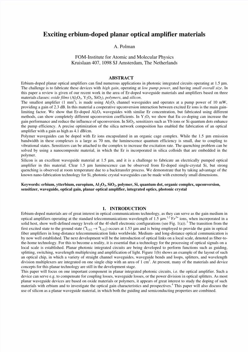
solid host, show well-defined energy levels of the 4f-shell electronic configurations (see Fig. 1(a)).3 The transition from the
first excited state to the ground state (4I13/2 → 4I15/2) occurs at 1.53 µm and is being employed to provide the gain in optical
fiber amplifiers in long-distance telecommunication links worldwide. Medium- and long-distance optical communication is
by now well established. The next development will be the introduction of optical links on a local scale, denoted as fiber-to-the-home technology. For this to become a reality, it is essential that a technology for the processing of optical signals on a
local scale is established. Planar photonic integrated circuits are being developed to perform functions such as guiding,splitting, switching, wavelength multiplexing and amplification of light. Figure 1(b) shows an example of the layout of such
an optical chip, in which a variety of straight channel waveguides, waveguide bends and loops, splitters, and wavelength
division multiplexers are integrated on one single chip with an area of 1 cm2. At present, many of the materials and device
concepts for this planar technology are still in the development stage.This paper will focus on one important component in planar integrated photonic circuits, i.e. the optical amplifier. Such a
device can serve e.g. to compensate for coupling losses, waveguide losses, or the power division in optical splitters. As most
planar waveguide devices are based on oxide materials or polymers, it appears of great interest to study the doping of such
materials with erbium and to investigate the optical gain characteristics and prospectives.4 This paper will also discuss the
use of silicon as a planar waveguide material, in which both the guiding and semiconducting properties are combined.
8/10/2019 Erbium-doped OpAmp
http://slidepdf.com/reader/full/erbium-doped-opamp 2/12
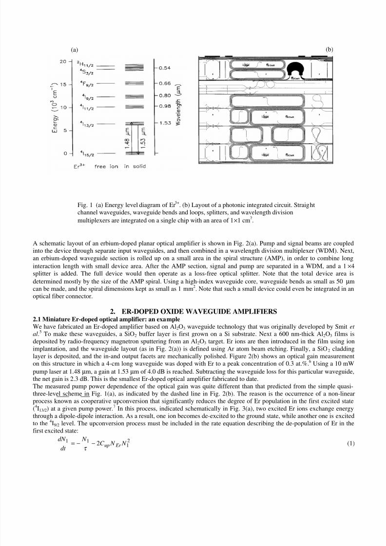
A schematic layout of an erbium-doped planar optical amplifier is shown in Fig. 2(a). Pump and signal beams are coupled
into the device through separate input waveguides, and then combined in a wavelength division multiplexer (WDM). Next,
an erbium-doped waveguide section is rolled up on a small area in the spiral structure (AMP), in order to combine long
interaction length with small device area. After the AMP section, signal and pump are separated in a WDM, and a 1 ×4
splitter is added. The full device would then operate as a loss-free optical splitter. Note that the total device area is
determined mostly by the size of the AMP spiral. Using a high-index waveguide core, waveguide bends as small as 50 µm
can be made, and the spiral dimensions kept as small as 1 mm2. Note that such a small device could even be integrated in anoptical fiber connector.
2. ER-DOPED OXIDE WAVEGUIDE AMPLIFIERS2.1 Miniature Er-doped optical amplifier: an example
We have fabricated an Er-doped amplifier based on Al2O3 waveguide technology that was originally developed by Smit et
al.5 To make these waveguides, a SiO2 buffer layer is first grown on a Si substrate. Next a 600 nm-thick Al2O3 films is
deposited by radio-frequency magnetron sputtering from an Al2O3 target. Er ions are then introduced in the film using ion
implantation, and the waveguide layout (as in Fig. 2(a)) is defined using Ar atom beam etching. Finally, a SiO 2 cladding
layer is deposited, and the in-and output facets are mechanically polished. Figure 2(b) shows an optical gain measurement
on this structure in which a 4-cm long waveguide was doped with Er to a peak concentration of 0.3 at.%.6 Using a 10 mW
pump laser at 1.48 µm, a gain at 1.53 µm of 4.0 dB is reached. Subtracting the waveguide loss for this particular waveguide,the net gain is 2.3 dB. This is the smallest Er-doped optical amplifier fabricated to date.
The measured pump power dependence of the optical gain was quite different than that predicted from the simple quasi-
three-level scheme in Fig. 1(a), as indicated by the dashed line in Fig. 2(b). The reason is the occurrence of a non-linear
process known as cooperative upconversion that significantly reduces the degree of Er population in the first excited state
(4I13/2) at a given pump power.
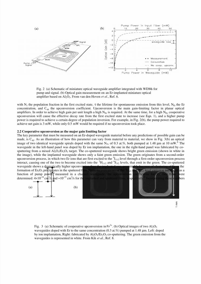
7 In this process, indicated schematically in Fig. 3(a), two excited Er ions exchange energy
through a dipole-dipole interaction. As a result, one ion becomes de-excited to the ground state, while another one is excited
to the 4I9/2 level. The upconversion process must be included in the rate equation describing the de-population of Er in the
first excited state:
21
11 2 N N C N
dt
dN Er up−−=
τ
(1)
Fig. 1 (a) Energy level diagram of Er3+
. (b) Layout of a photonic integrated circuit. Straight
channel waveguides, waveguide bends and loops, splitters, and wavelength division
multiplexers are integrated on a single chip with an area of 1×1 cm2.
(a) (b)
8/10/2019 Erbium-doped OpAmp
http://slidepdf.com/reader/full/erbium-doped-opamp 3/12
with N1 the population fraction in the first excited state, τ the lifetime for spontaneous emission from this level, NEr the Erconcentration, and Cup the upconversion coefficient. Upconversion is the main gain-limiting factor in planar optical
amplifiers. In order to achieve high gain per unit length a high NEr is required. At the same time, for a high NEr, cooperative
upconversion will cause the effective decay rate from the first excited state to increase (see Eqn. 1), and a higher pump
power is required to achieve a certain degree of population inversion. For example, in Fig. 2(b), the pump power required to
achieve net gain is 3 mW, while only 0.5 mW would be required if no upconversion took place.
2.2 Cooperative upconversion as the major gain limiting factor
The key parameter that must be measured on an Er-doped waveguide material before any predictions of possible gain can be
made, is Cup. As an illustration of how this parameter can vary from material to material, we show in Fig. 3(b) an optical
image of two identical waveguide spirals doped with the same NEr of 0.3 at.%, both pumped at 1.48 µm at 10 mW.8 The
waveguide in the left-hand panel was doped by Er ion implantation, the one in the right-hand panel was fabricated by co-
sputtering from a mixed Al2O3 /Er2O3 target. The co-sputtered waveguide shows bright green emission (shown in white inthe image), while the implanted waveguide shows only a faint green emission. The green originates from a second-order
upconversion process, in which two Er ions that are first excited to the4I11/2 level through a first-order upconversion process
interact, causing one of the two to become excited into the 2H11/2 and 4S3/2 levels, that emit in the green. The co-sputtered
waveguide shows a dramatically higher upconversion than the implanted one, presumably because of clustering of Er or the
formation of Er2O3 precipitates in the sputtered film. From measurements of the4I13/2 and
4I11/2 level emission intensities as a
function of pump power, measured in a channel waveguide, the upconversion coefficients for the two films were
determined: 4×10-18
cm3 /s and ≈10
-15 cm
3 /s for the implanted and sputtered films, respectively.
8 Incorporating these numbers
Fig. 2 (a) Schematic of miniature optical waveguide amplifier integrated with WDMs for
pump and signal. (b) Optical gain measurement on an Er-implanted miniature optical
amplifier based on Al2O3. From van den Hoven et al., Ref. 6.
1 m m
Fig. 3 (a) Schematic of cooperative upconversion in Er3+
. (b) Optical images of two Al2O3
waveguides doped with Er to the same concentration (0.3 at.%) pumped at 1.48 µm. Left: doped
by ion implantation, Right: fabricated by Al2O3 /Er2O3 co-sputtering. The green emission from the
waveguides is represented in white. From Kik et al., Ref. 8.
(a) (b)
(a) (b)
8/10/2019 Erbium-doped OpAmp
http://slidepdf.com/reader/full/erbium-doped-opamp 4/12
in Eqn. (1), the effective Er decay rate can be calculated for the two waveguides, assuming NEr = 0.3 at.% Er, and 50 %
inversion. The results are shown in Table I, together with the spontaneous decay rate for Er in Al2O3 in the case without
upconversion. Clearly, a very high pump power is required to compensate for the increased decay rate in the sputtered film.
The fabrication of Er-doped optical amplifier materials should therefore focus on atomic-scale engineering of the local
environment and distribution of Er such that upconversion is minimized.
Table I: Er 4I13/2 level decay rate in Al2O3 for three upconversion coefficients4I13/2 level decay rate (s-1)
no upconversion (Cup = 0) 130
Er implanted waveguide (Cup = 4×10-18 cm3 /s) 700
co-sputtered waveguide (Cup = ≈10-15
cm3 /s) ≈10
5
A parameter that is of key importance in determining weather net gain will be observed, given a known upconversioncoefficient, is the mode confinement in the waveguide. Even for a relatively low upconversion coefficient, an Er excitation
rate of order >1000 s-1 is required to achieve inversion (see Table I). At the typical Er absorption cross section of 3×10-21
cm2, this corresponds to a power density in the waveguide > 50 kW/cm
2. In a well-confined waveguide with mode
dimensions on the order of 1×1 µm2, such as the Al2O
3 structure shown above, this can be achieved at a pump power of a
few mW. However, in a silica glass planar waveguide defined by e.g. an ion-exchange process with small index contrast,
optical modes may be as large as 5×5 µm2 and hence the pump power to reach inversion may well exceed 100 mW.9,10
An example of a waveguide material that combines low upconversion with high index contrast is a multi-component
phosphosilicate glass developed by Yan et al.11 It is composed of Er2O3, Al2O3, Na2O, La2O3, and P2O5. P2O5-based glasses
are known to be a good host for Er without clustering and indeed, the upconversion coefficient in this glass is only 2 ×10-18
cm3 /s, the lowest value reported for a glass material. Na2O is added as a network modifier, Al2O3 to increase the chemical
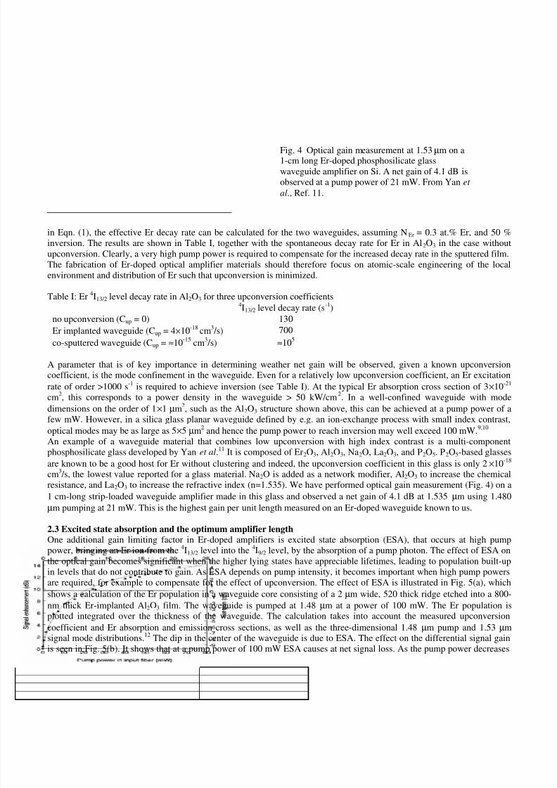
resistance, and La2O3 to increase the refractive index (n=1.535). We have performed optical gain measurement (Fig. 4) on a
1 cm-long strip-loaded waveguide amplifier made in this glass and observed a net gain of 4.1 dB at 1.535 µm using 1.480
µm pumping at 21 mW. This is the highest gain per unit length measured on an Er-doped waveguide known to us.
2.3 Excited state absorption and the optimum amplifier length
One additional gain limiting factor in Er-doped amplifiers is excited state absorption (ESA), that occurs at high pump
power, bringing an Er ion from the4
I13/2 level into the4
I9/2 level, by the absorption of a pump photon. The effect of ESA onthe optical gain becomes significant when the higher lying states have appreciable lifetimes, leading to population built-up
in levels that do not contribute to gain. As ESA depends on pump intensity, it becomes important when high pump powers
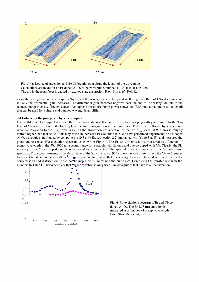
are required, for example to compensate for the effect of upconversion. The effect of ESA is illustrated in Fig. 5(a), which
shows a calculation of the Er population in a waveguide core consisting of a 2 µm wide, 520 thick ridge etched into a 800-
nm thick Er-implanted Al2O3 film. The waveguide is pumped at 1.48 µm at a power of 100 mW. The Er population isplotted integrated over the thickness of the waveguide. The calculation takes into account the measured upconversion
coefficient and Er absorption and emission cross sections, as well as the three-dimensional 1.48 µm pump and 1.53 µmsignal mode distributions.12 The dip in the center of the waveguide is due to ESA. The effect on the differential signal gain
is seen in Fig. 5(b). It shows that at a pump power of 100 mW ESA causes at net signal loss. As the pump power decreases
Fig. 4 Optical gain measurement at 1.53 µm on a1-cm long Er-doped phosphosilicate glass
waveguide amplifier on Si. A net gain of 4.1 dB is
observed at a pump power of 21 mW. From Yan et
al., Ref. 11.
8/10/2019 Erbium-doped OpAmp
http://slidepdf.com/reader/full/erbium-doped-opamp 5/12
along the waveguide due to absorption (by Er and the waveguide structure) and scattering, the effect of ESA decreases andinitially the differential gain increases. The differential gain becomes negative near the end of the waveguide due to the
reduced pump intensity. The existence of an upper limit on the pump power shows that ESA puts a maximum to the length
that can be used for a single-end pumped waveguide amplifier.
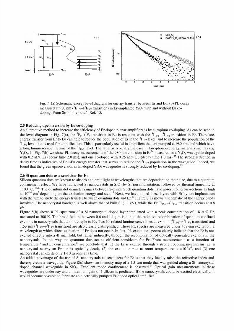
2.4 Enhancing the pump rate by Yb co-doping
One well-known technique to enhance the effective excitation efficiency of Er is by co-doping with ytterbium.13 As the 2F5/2
level of Yb is resonant with the Er4I11/2 level, Yb→Er energy transfer can take place. This is then followed by a rapid non-
radiative relaxation to the 4I13/2 level in Er. As the absorption cross section of the Yb 2F5/2 level (at 975 nm) is roughly
tenfold higher than that of Er,14
this may cause an increased Er excitation rate. We have performed experiments on Er-doped
Al2O3 waveguides fabricated by co-sputtering (0.3 at.% Er, see section 2.2) implanted with Yb (0.3 at.%), and measured the
photoluminescence (PL) excitation spectrum as shown in Fig. 6.14
The Er 1.5 µm emission is measured as a function of pump wavelength in the 900-1020 nm spectral range for a sample with Er only and one co-doped with Yb. Clearly, the PL
intensity in the Yb co-doped sample is enhanced by a factor ten. The spectral shape corresponds to the Yb absorption
spectrum. From measurements of the decay time of the Yb emission at 975 nm we have also determined the Yb→Er energytransfer rate, it amounts to 2500 s-1. It is important to realize that the energy transfer rate is determined by the Er
concentration and distribution. It can not be increased by increasing the pump rate. Comparing the transfer rate with thenumbers in Table I, it becomes clear that Yb sensitization is only useful in waveguides that have low upconversion.
17 cm
12 m
17 cm
12 m
Fig. 5 (a) Degree of inversion and (b) differential gain along the length of the waveguide.
Calculations are made for an Er-doped Al2O3 ridge waveguide, pumped at 100 mW at 1.48 µm.
The dip in the front facet is caused by excited state absorption. From Kik et al., Ref. 12.
900 920 940 960 980 1000 1020
0.0
1.0
2.0
3.0
4.0
5.0
6.0
Er:Yb:Al2O
3
Er:Al2O
3
4 I 1 3 / 2
i n t e n s i t y [ a . u . ]
excitation wavelength [nm]
Fig. 6 PL excitation spectrum of Er and Yb co-
doped Al2O3. The Er 1.53 µm emission ismeasured as a function of pump wavelength.
From Strohhöfer et al, Ref. 14.
(a) (b)
8/10/2019 Erbium-doped OpAmp
http://slidepdf.com/reader/full/erbium-doped-opamp 6/12
2.5 Reducing upconversion by Eu co-doping
An alternative method to increase the efficiency of Er-doped planar amplifiers is by europium co-doping. As can be seen in
the level diagram in Fig. 7(a), the7F0→
7F4 transition in Eu is resonant with the 4I11/2→4I13/2 transition in Er. Therefore,
energy transfer from Er to Eu can help to reduce the population of Er in the 4I11/2 level, and to increase the population of the4I13/2 level that is used for amplification. This is particularly useful in amplifiers that are pumped at 980 nm, and which have
a long luminescence lifetime of the4I11/2 level. The latter is typically the case in low-phonon energy materials such as e.g.
Y2O3. In Fig. 7(b) we show PL decay measurements of the 980 nm emission in Er3+ measured in a Y2O3 waveguide doped
with 0.2 at.% Er (decay time 2.0 ms), and one co-doped with 0.25 at.% Eu (decay time 1.0 ms).15 The strong reduction in
decay time is indicative of Er→Eu energy transfer that serves to reduce the 4I11/2 population in the waveguide. Indeed, wefound that the green upconversion in Er-doped Y2O3 waveguides is strongly reduced by Eu co-doping.15
2.6 Si quantum dots as a sensitizer for Er
Silicon quantum dots are known to absorb and emit light at wavelengths that are dependent on their size, due to a quantum
confinement effect. We have fabricated Si nanocrystals in SiO2 by Si ion implantation, followed by thermal annealing at
1100 °C. 16,17 The quantum dot diameter ranges between 2–5 nm. Such quantum dots have absorption cross-sections as high
as 10-14 cm2 depending on the excitation energy and size.18 Next, we have doped these layers with Er by ion implantation
with the aim to study the energy transfer between quantum dots and Er.19 Figure 8(a) shows a schematic of the energy bands
involved. The nanocrystal bandgap is well above that of bulk Si (1.1 eV), while the Er 4I15/2→4I13/2 transition occurs at 0.8
eV.
Figure 8(b) shows a PL spectrum of a Si nanocrystal-doped layer implanted with a peak concentration of 1.8 at.% Er,
measured at 300 K. The broad feature between 0.6 and 1.1 µm is due to the radiative recombination of quantum-confined
excitons in nanocrystals that do not couple to Er. Two Er-related luminescence lines at 980 nm (4I11/2→ 4I15/2 transition) and
1.53 µm (4I13/2→4I15/2 transition) are also clearly distinguished. These PL spectra are measured under 458-nm excitation, a
wavelength at which direct excitation of Er does not occur. In fact, PL excitation spectra clearly indicate that the Er is notexcited directly into a 4f manifold, but rather indirectly, through the recombination of optically generated excitons in the
nanocrystals. In this way the quantum dots act as efficient sensitizers for Er. From measurements as a function of
temperature19 and Er concentration20 we conclude that (1) the Er is excited through a strong coupling mechanism (i.e. a
nanocrystal nearby an Er ion is optically dead), (2) the excitation rate at room temperature is >106s
-1, and (3) one
nanocrystal can excite only 1-10 Er ions at a time.
An added advantage of the use of Si nanocrystals as sensitizers for Er is that they locally raise the refractive index and
thereby create a waveguide. Figure 8(c) shows an intensity map of a 1.5 µm mode that was guided along a Si nanocrystaldoped channel waveguide in SiO2. Excellent mode confinement is observed.21 Optical gain measurements in these
waveguides are underway and a maximum gain of 1 dB/cm is predicted. If the nanocrystals could be excited electrically, it
would become possible to fabricate an electrically pumped Er-doped optical amplifier.
Fig. 7 (a) Schematic energy level diagram for energy transfer between Er and Eu. (b) PL decay
measured at 980 nm (4I11/2→4I15/2 transition) in Er-implanted Y2O3 with and without Eu co-
doping. From Strohhöfer et al., Ref. 15.
(a) (b)
8/10/2019 Erbium-doped OpAmp
http://slidepdf.com/reader/full/erbium-doped-opamp 7/12
3. ER-DOPED POLYMER WAVEGUIDE AMPLIFIER MATERIALSThe importance of polymer optical waveguide technology is growing rapidly. First of all, polymer fibers are used more andmore in short-distance optical links. Also, thin film integrated optical devices based on polymers become important. It
would be of great interest to dope a polymer waveguide with Er in order to fabricate a polymer-based optical amplifier.
Unfortunately, the erbium salts typically used in wet chemical processing are insoluble in the polymer precursors. To
overcome this problem, we have studied two routes.
3.1 Er-doped organic cage complexesWe have designed a cyclic polydentate organic cage complex in which a rare earth ion is embedded (see Fig. 9(a)), that can
be easily dissolved in a polymer matrix.22,23 In such a complex, the Er can be excited indirectly through the aromatic rings of
the ligands that have a high absorption cross section. The Er luminescence spectrum is extremely broad, with a full width at
half-maximum of 70 nm, enabling a high gain bandwidth.22 Unfortunately, the Er ions embedded in these complexes show
large luminescence quenching, presumably due to coupling to vibrational states of the C–H bond in the complex itself, orO–H bonds in the solvents in which these complexes are processed. By selectively deuterating sections of the complex, andusing deuterated solutions in the processing, the quenching can be slightly reduced,24 but the highest luminescence lifetime
at 1.53 µm, measured in DMSO-d6 solution, is 5.4 µs, well below the estimated radiative lifetime of 4 ms.
Si
Er3+
SiO2
(a) (b)
-6 -4 -2 0 2 4 6
-6
-4
-2
0
2
4
6
X Axis
Y A x i s
156.3 -- 1
142.5 -- 1
128.8 -- 1
115.0 -- 1
101.3 -- 1
87.50 -- 1
73.75 -- 8
60.00 -- 7
Fig. 8 (a) Schematic of energy levels involved in energy transfer between Si quantum dots and Er. (b) PL
spectrum of Er-doped Si nanocrystal-doped SiO2 measured at room temperature. Pump wavelength 458 nm.
(c) Optical mode profile at 1.5 µm of a Si nanocrystal-doped channel waveguide in SiO2. From Kik et al., Refs.
19, 20, 21.
(a) c
0
5000
10000
15000
20000
1O
2
3O
2
radiationlessdeactivation
4S
3/2
1 3
4 0 n m
8 9 0 n m
e x c
i t a t i o n
1 0 6 0 n m
energy transfer
crossingintersystem
e x c i t a t i o n
f l u o r e s c e n c e
2K
13/2
4F
9/2
4G
7/2
4G
5/2
E n e r g y ( c m
- 1 ) 4
F5/2
4F
3/2
4I15/2
4I
13/2
4I11/2
4I9/2
T
S1
S0
Nd3+
lissamine
Fig. 9 (a) Schematic of cyclic polydentate organic cage complex in which a rare earth ion is embedded.
(b) Energy transfer processes in a lissamine sensitized Nd-complex. From Slooff et al., Refs. 22, 25 and
Klink et al., Ref. 23.
(a) (b)
0.6 0.8 1.00
2
4
6
8
10
12
Wavelength (µm)
P L I n t e n s i t y
( a . u . )
1.5 1.6 1.7
b
X
Y

8/10/2019 Erbium-doped OpAmp
http://slidepdf.com/reader/full/erbium-doped-opamp 8/12
With such a high PL decay rate, very high pump powers are required to achieve inversion. To overcome this, a sensitizer
can be attached to the complex, such as e.g. lissamine. Figure 9(b) shows the energy level diagram of a lissamine sensitizer,
coupled to a Nd ion in a terphenyl-based complex.25 The sensitizer can be excited very efficiently into the singlet state
(cross section >10-17 cm2 at 500 nm). After rapid intersystem crossing to the triplet state, energy transfer can take place to
the Nd ion, leading to excitation into the 4S3/2 and 4F9/2 levels. After relaxation to the 4F3/2 level, luminescence at 890, 1060,
and 1340 nm is observed. The intramolecular energy transfer rate is as large as 107 s-1. These complexes can be embedded in
a perfluorinated planar polymer waveguide with optical losses of 0.2 dB/cm at 1.5 µm.25 Concentrations as high as 10 wt.%can be dissolved in the polymer. One problem in these waveguides is the strong photodegradation of the Nd luminescence
that is observed upon continued optical pumping.26
This photodegradation may be related to the presence of oxygen in the
waveguide film, resulting in bleaching of the sensitizer. Such a problem could be overcome by using the proper steps in the
waveguide processing.
3.2 Er-doped organic/inorganic nanocomposite waveguidesAn alternative method to incorporate Er in a polymer waveguide is by using a nanocomposite material composed of Er-
doped SiO2 colloids embedded in a polymer. In this way the excellent properties of both materials: SiO 2 as a good host for
Er, and the easy polymer processing, are combined. We have fabricated 360-nm diameter SiO 2 colloids by wet chemical
processing using tetraethoxysilane (see Fig. 10(a)), and implanted them with Er to concentrations in the range 0.2–1.1
at.%.27
Figure 10(b) shows a PL spectrum taken using excitation at 488 nm. PL lifetimes as high as 17 ms are observed,
corresponding to a luminescence quantum efficiency as high as 80 %. The long lifetime is partly ascribed to the fact that theimplanted colloids are mostly surrounded by air, with a low refractive index, and hence the local optical density of states in
the colloids is relatively low, leading to a small radiative decay rate.28
Optical gain calculations show that if these colloids
could be embedded in a high-index-contrast waveguide with well-confined modes, an optical gain of 4 dB could be
achieved for a 3-cm long waveguide at a pump power of only 10 mW. This calculation assumes an upconversion coefficient
of 3×10-18 cm3 /s, similar to that found for sodalime glass.9
4. ER-DOPED SILICON WAVEGUIDE AMPLIFIER MATERIALSSilicon is one of the best known materials in the world. It is available in high purity and the processing technologies for
silicon are by now very well established. While the properties of silicon as a semiconductor are well explored, it is not much
used in photonic technology. However, Si is an excellent optical waveguide material, as it is completely transparent at 1.5
µm. If Si could be doped with high concentrations of optically active Er, an electrically pumped Er-doped amplifier could
be made.Figure 11(a) shows a schematic energy level diagram for Er-doped Si.29 It resembles that for the Si nanocrystal-Er coupling
scheme in Fig. 8(a), with the exception that the Si bandgap energy is now fixed at 1.1 eV, and that the exciton trapping takes
place due to the presence of an Er-related defect state in the Si bandgap. As observed by many groups,30 surface layers of
single crystal Si doped with Er show clear Er-related PL at 1.53 µm under optical excitation at 488 nm. PL excitation
1.40 1.45 1.50 1.55 1.60 1.65 1.700.0
0.5
1.0
1.535 µm
1.1 at.%
P L I n t e n s i t y
( m V )
Wavelength (µm)
Fig. 10 (a) Scanning electron micrograph 360-nm diameter silica colloids deposited on a Si substrate.
(b) PL spectrum of Er-implanted silica colloids, pumped at 488 nm From Slooff et al., Ref. 27.
(a) (b)
8/10/2019 Erbium-doped OpAmp
http://slidepdf.com/reader/full/erbium-doped-opamp 9/12
spectroscopy shows that the excitation takes place in a three-step process in which (1) optically generated electron-hole
pairs form an exciton trapped at the Er-related defect, (2) an impurity Auger process takes place in which the exciton
recombines and energy is transferred to Er that then becomes excited into the 4I13/2 level, and (3) the Er decays by the
emission of a photon at 1.53 µm. Figure 11(b) shows the temperature dependence of the Er PL intensity and lifetime.29 Ascan be seen, both show strong quenching at temperatures above 150 K. The quenching is mostly due to a backtransfer
process, in which excited Er de-excites by the generation of the bound exciton state (WBT in Fig. 11(a)) . This may seem an
improbable process, as it requires at additional 150 meV to bridge the gap between the Er 4I13/2 energy and the exciton level,but as the PL lifetime of the 4I13/2 state is very long (1 ms), this backtransfer process can actually be quite efficient.
Eventually, the re-generated exciton may dissociate (WT in Fig. 11(a)), leading to the generation of a free electron-hole pair
that can be collected from a p-n junction. Temperature-dependent measurements of the 1.5 µm photocurrent of an Er-doped
Si p-n junction are also included in Fig. 11(b).29
Indeed, the photocurrent increases with temperature as expected for aphonon-assisted process. By fitting a rate-equation model to the three data sets in Fig. 11(b) we have identified all rate
constants and activation energies in the diagram of Fig. 11(a).29 We found that the internal quantum efficiency for the
complete backtransfer process is as high at 70 % at room temperature. Er-doped Si waveguides could therefore serve as an
infrared detector operating at 1.5 µm.
Several research groups have put significant effort in atomic-scale engineering of the Er site in Si such to minimize thequenching.31,32 It has been found that the addition of small concentrations of oxygen affects the local coordination for Er,
and leads to smaller quenching. Indeed, weak room temperature PL of Er/O-doped Si has been observed both under optical
and electrical excitation.30 The challenge is now to further reduce this quenching and to increase the optically active fraction
of Er. A fundamental problem that has been identified is the fact that Er can decay non-radiatively by an Auger process in
which free carriers are excited high in the conduction/valence band.33 Such carriers are provided by the Er itself, as Er (in
particular in the presence of impurities such as O) shows donor behavior in Si. Efficient Er-doped Si waveguide amplifiers
can therefore only be made if an Er site in Si is found that is optically active with small quenching, and at the same time is
not (or only slightly) electrically active.
5. THE ULTIMATE MINIATURIZATION: PHOTONIC BANDGAP WAVEGUIDESThe size of a photonic integrated circuit is often determined by the smallest waveguide bending radius that can be made. For
example, in the device layout of Fig. 1(b) for Al2O3, the minimum radius is 50 µm. Thus, the total area of the amplifier
spirals in Fig. 3(b) is 1 mm2. The radius could be further reduced by using a higher-index core material. Alternatively, a
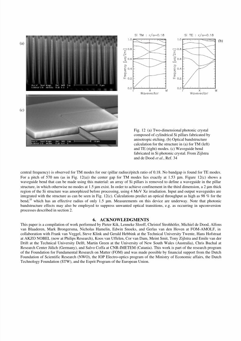
photonic bandgap effect may be used. As an example, we show our work on two-dimensional photonic crystals made of Si
pillars. Figure 12(a) shows an array of 5 µm tall Si pillars, 205 nm in diameter, arranged in a square lattice with 570 nmpitch, made by deep anisotropic etching using an SF6 /O2 electron cyclotron resonance driven plasma.34 Optical
bandstructure calculations for this structure are shown in Fig. 12(b) for TM and TE modes. A large bandgap (37 % of the
WBT
WEWT
WD
Ec
Ev
WA,e
WA,h
gE r W
0 W R
4I13/2
4I15/2
ET
EBT
Silicon Er3+
0 20 40 60 80
0.01
0.1
1
10
0.01
0.1
1
10
(I)(II)(III)
photocurrent
P h o t o c u r r e n t ( n A
)
intensity
lifetime
P L i n t e n s i t y ( a . u . ) a n d l i f e
t i m e ( m s )
1000/T (K-1)
Fig. 11 (a) Schematic energy level diagram for Er-doped crystalline Si. (b) Arrhenius plot of the temperature
dependence of 1.53 µm PL intensity and lifetime in Er-implanted Si p-n junction under optical excitation at 488nm. Data for the 1.5 µm photocurrent are also included. From Hamelin et al., Ref. 29.
(a) (b)
8/10/2019 Erbium-doped OpAmp
http://slidepdf.com/reader/full/erbium-doped-opamp 10/12
central frequency) is observed for TM modes for our (pillar radius)/pitch ratio of 0.18. No bandgap is found for TE modes.
For a pitch of 570 nm (as in Fig. 12(a)) the center gap for TM modes lies exactly at 1.53 µm. Figure 12(c) shows awaveguide bend that can be made using this material: an array of Si pillars is removed to define a waveguide in the pillar
structure, in which otherwise no modes at 1.5 µm exist. In order to achieve confinement in the third dimension, a 2 µm thick region of the Si structure was amorphized before processing, using 4 MeV Xe irradiation. Input and output waveguides are
integrated with the structure as can be seen in Fig. 12(c). Calculations predict an optical throughput as high as 98 % for the
bend,35 which has an effective radius of only 1.5 µm. Measurements on this device are underway. Note that photonic
bandstructure effects may also be employed to suppress unwanted optical transitions, e.g. as occurring in upconversion
processes described in section 2.
6. ACKNOWLEDGMENTSThis paper is a compilation of work performed by Pieter Kik, Lenneke Slooff, Christof Strohhöfer, Michiel de Dood, Alfons
van Blaaderen, Mark Brongersma, Nicholas Hamelin, Edwin Snoeks, and Gerlas van den Hoven at FOM-AMOLF, in
collaboration with Frank van Veggel, Steve Klink and Gerald Hebbink at the Technical University Twente, Hans Hofstraat
at AKZO NOBEL (now at Philips Research), Koos van Uffelen, Cor van Dam, Meint Smit, Tony Zijlstra and Emile van derDrift at the Technical University Delft, Martin Green at the University of New South Wales (Australia), Chris Buchal at
Research Center Jülich (Germany), and Salvo Coffa at CNR-IMETEM (Catania). This work is part of the research program
of the Foundation for Fundamental Research on Matter (FOM) and was made possible by financial support from the Dutch
Foundation of Scientific Research (NWO), the IOP Electro-optics program of the Ministry of Economic affairs, the Dutch
Technology Foundation (STW), and the Esprit Program of the European Union.
Fig. 12 (a) Two-dimensional photonic crystal
composed of cylindrical Si pillars fabricated by
anisotropic etching. (b) Optical bandstructure
calculation for the structure in (a) for TM (left)and TE (right) modes. (c) Waveguide bend
fabricated in Si photonic crystal. From Zijlstra
and de Dood et al., Ref. 34
(c)
(a)(b)
8/10/2019 Erbium-doped OpAmp
http://slidepdf.com/reader/full/erbium-doped-opamp 11/12
7. REFERENCES
1 W.J. Miniscalco, “Erbium-doped glasses for fiber amplifiers at 1500 nm”, J. Lightwave Technol., p. 234, 19912 E. Desurvire, Erbium-doped fiber amplifiers: principles and applications, John Wiley & Sons, 19943 S. Hüffner, Optical spectra of transparent rear-earth compounds, Academic, New York, 1978
4
see for a review of earlier work: A. Polman, “Erbium implanted thin film photonic materials”, J. Appl. Phys. 82, p. 1,1997.5 M.K. Smit, Integrated optics in silicon-based aluminium oxide, Ph.D. Thesis, Delft University of Technology, 1991
6 G.N. van den Hoven, A. Polman, C. van Dam, J.W.M. van Uffelen, and M.K. Smit, “Net optical gain at 1.53 µm in Er-
doped Al2O3 waveguides on silicon”, Appl. Phys. Lett. 68 , p. 1886, 19967 G.N. van den Hoven, E. Snoeks, A. Polman, C. van Dam, J.W.M. van Uffelen, and M.K. Smit, “Upconversion in Er-
implanted Al2O3 waveguides”, J. Appl. Phys. 79, p. 1258, 19968 P.G. Kik and A. Polman, to be published.9 E. Snoeks, G.N. van den Hoven, A. Polman, B. Hendriksen, M.B.J. Diemeer, and F. Priolo, “Cooperative upconversion in
erbium implanted sodalime silicate glass optical waveguides”, J. Opt. Soc. Am. B 12, p. 1468, 199510 E. Snoeks, G.N. van den Hoven, and A. Polman, “Optimization of an Er-doped silica glass optical waveguide amplifier”,
IEEE J. Quantum Electron. 32, p. 1680, 199611 Y.C. Yan, A.J. Faber, H. de Waal, P.G. Kik, and A. Polman, “Erbium-doped phosphate glass waveguide on silicon with
4.1 dB/cm gain at 1.535 µm”, Appl. Phys. Lett. 71, p. 2922, 199712
P.G. Kik and A. Polman, to be published.13 M.P. Hehlen, N.J. Cockroft, T.R. Gosnell, A.J. Bruce, “Spectroscopic properties of Er3+- and Yb3+-doped soda-lime
silicate and aluminosilicate glasses”, Phys. Rev. B 56 , p. 9302, 199714
Ch. Strohhöfer, P.G. Kik, and A. Polman, to be published15 Ch. Strohhöfer, P.G. Kik, and A. Polman, “Selective modification of the Er3+ 4I11/2 branching ratio by energy transfer to
Eu3”, submitted to J. Appl. Phys. 200016
K.S. Min, K.V. Shcheglov, C.M.Yang, H.A. Atwater, M.L. Brongersma and A. Polman, “Defect-related versus excitonic
visible light emission from ion beam synthesized Si nanocrystals in SiO2”, Appl. Phys. Lett. 69, p. 2033, 199617 M.L. Brongersma, P.G. Kik, A. Polman, K.S. Min, and H.A. Atwater, “Size dependent electron-hole exchange splitting in
Si nanocrystals”, Appl. Phys. Lett., 76 , p. 351, 200018 D. Kovalev, J. Diener, H. Heckler, G. Polisski, N. Künzer, and F. Koch, “Optical absorption cross sections of Si
nanocrystals”, Phys. Rev. B 61, p. 4485, 200019 P.G.Kik, M.L. Brongersma, and A. Polman , “Strong exciton-erbium coupling in Si nanocrystal doped SiO2” , Appl. Phys.
Lett., 76 , 2000, in press20 P.G. Kik, and A. Polman, “Maximum excitable Er concentration in Si nanocrystal-doped SiO2”, submitted to J. Appl.
Phys., 200021 P.G. Kik and A. Polman, to be published.22 L.H. Slooff, A. Polman, M.P. Oude Wolbers, F.C.J.M. van Veggel, D. Reinhoudt, and J.W. Hofstraat, “Optical properties
of erbium-doped polydentate organic cage complexes”, J. Appl. Phys. 83, p. 497, 199823 S.I. Klink, G.A. Hebbink, L. Grave, F.C.J.M. van Veggel, D.N. Reinhoudt, L.H. Slooff, A. Polman, and J.W. Hofstraat,
“Sensitized near-infrared luminescence from polydentate triphenylene-functionalized Nd3+, Yb3+, and Er3+ complexes”, J.
Appl. Phys. 86, p. 1181, 199924 G.A. Hebbink et al, to be published25 L.H. Slooff, A. Polman, S.I. Klink, G.A. Hebbink, L. Grave, F.C.J.M. van Veggel, D.N. Reinhoudt, and J.W. Hofstraat,
“Optical properties of lissamine functionalized Nd3+
complexes in polymer waveguides and solution”, Optical Materials 14,
p. 101, 2000.26 L.H. Slooff, A. Polman, S.I. Klink, G.A. Hebbink, L. Grave, F.C.J.M. van Veggel, D.N. Reinhoudt, and J.W. Hofstraat, to
be published27 L.H Slooff, M.J.A. de Dood, A. van Blaaderen, and A. Polman, “Erbium-implanted silica colloids with 80 %luminescence quantum efficiency”, submitted to Appl. Phys. Lett ., 200028
E. Snoeks, A. Lagendijk, and A. Polman, “Measuring and modifying the spontaneous emission rate of erbium near an
interface”, Phys. Rev. Lett. 74, p. 2460, 199529 N. Hamelin, P.G. Kik, J.F. Suyver, K. Kikoin, A. Polman, A. Schönecker, and F.W. Saris, “Energy backtransfer and
infrared photocurrent in erbium-doped silicon p-n junctions”, submitted to J. Appl. Phys. 2000

8/10/2019 Erbium-doped OpAmp
http://slidepdf.com/reader/full/erbium-doped-opamp 12/12
30 See for a review: “Light emission from Er-doped Si: Materials properties, mechanisms, and device performance”, S.
Coffa, G. Franzò, and F. Priolo, MRS Bulletin 23/4, p. 25, 199831 J. Michel, J.L. Benton, R.F. Ferrante, D.C. Jacobson, D.J. Eaglesham, E.. Fitzgerald, Y.-H. Xie, and L.C. Kimerling,
“Impurity enhancement of the 1.54 µm Er3+
luminescence in silicon”, J. Appl. Phys. 70, p. 2667, 199132 F. Priolo, G. Franzó, S. Coffa, A. Polman, S. Libertino, R. Barklie, and D. Carey, “The erbium-impurity interaction and
its effect on the 1.54 µm luminescence of Er3+
in silicon”, J. Appl. Phys. 78 , p. 3874, 199533 F. Priolo, G. Franzò, S. Coffa, and A. Carnera, “Excitation and nonradiative deexcitation processes of Er
3+ in crystalline
Si”, Phys. Rev. B 57 , p. 4443, 199834 T. Zijlstra, E.W.J.M. van der Drift, M.J.A. de Dood, E. Snoeks, and A. Polman, “Fabrication of two-dimensional photonic
crystal waveguides at 1.5 µm in silicon by deep anisotropic etching”, J. Vac. Sci. Technol. B17 , p. 2734, 199935 A. Mekis, J.C. Chen, I. Kurland, S. Fan, P.R. Villeneuve, and J.D. Joannopoulos, Phys. Rev. Lett. 77 , p. 3787, 1996


![Tunable Erbium-Doped Fiber Lasers Using Various Inline Fiber … · 2016-02-18 · erbium-doped fiber lasers [4], distributed feedback fiber lasers [5], and Brillouin erbium-doped](https://img.pdfslide.us/doc/110x75/5f5d6d92d306cb22521e3c0b/tunable-erbium-doped-fiber-lasers-using-various-inline-fiber-2016-02-18-erbium-doped.jpg)