Embed Size (px)
Citation preview

EPICS Collaboration Meeting, Hsinchu, Taiwan, June, 2011
NSLS-II Power Supply Control System
Yuke Tian
Accelerator Division
Photon Science Directory
Brookhaven National Lab

EPICS Collaboration Meeting, Hsinchu, Taiwan, June, 2011
Outline
1. NSLS-II power supply control systemSystem Overview Three types of PS operation mode PS control data flow
2. Application software and EPICS device support Engineer test screenPublic PV lists and databaseDevice support
3. Generic IOC-FPGA communication protocol Move data bwteen EPICS IOC and FPGA device
Genetic IOC-FPGA communication protocol
4. Hardware level

EPICS Collaboration Meeting, Hsinchu, Taiwan, June, 2011
Standards for Main Dipole Magnet Standards for Quardupole Magnet Standards for Sextupole Magnet
SC
FCFC
FC
FC
FC
FC
SC SCSC
SC
SC
SC SCSC
SC
SC
SC
FC Standards for Fast Corrector Magnet SC Standards for Slow Corrector Magnet
Dipole
Dipole
Magnets and Power Supplies in Storage Ring
System Overview
EPICS Collaboration Meeting, Hsinchu, Taiwan, June, 2011
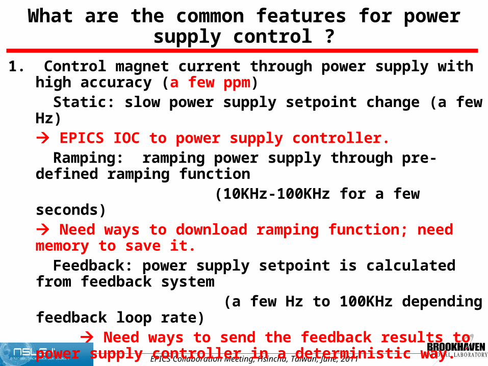
What are the common features for power supply control ?
1. Control magnet current through power supply with high accuracy (a few ppm) Static: slow power supply setpoint change (a few Hz)
EPICS IOC to power supply controller. Ramping: ramping power supply through pre-defined ramping function (10KHz-100KHz for a few seconds)
Need ways to download ramping function; need memory to save it. Feedback: power supply setpoint is calculated from feedback system (a few Hz to 100KHz depending feedback loop rate) Need ways to send the feedback results to power supply controller in a
deterministic way. 2. To synchronize magnets behavior Need interface to timing system 3. A lot of power supply/magnets diagnostic data:
Need a lot of ADCs, digital inputs/outputs Need a large memory to save the diagnostic data

EPICS Collaboration Meeting, Hsinchu, Taiwan, June, 2011
Let’s build a power supply control system
Power
Amp
Magnet
DCCT
High precision DAC
(20-bit)
FPGA
FPGA
EPICS IOC
TCP/IP
Fiber
Many ADCs
(16-bit)
Large memory
(DDR2/DDR3)
Triggers from timing system
Deterministic link to FOFB

EPICS Collaboration Meeting, Hsinchu, Taiwan, June, 2011
Let’s build a digital power supply control system
Power
Amp
Magnet
DCCTDigital
regulator
FPGA
FPGA
EPICS IOC
TCP/IP
Fiber
Many ADCs
(16-bit)
Large memory
(DDR2/DDR3)
Triggers from timing system
Deterministic link to FOFB
High precision ADC

EPICS Collaboration Meeting, Hsinchu, Taiwan, June, 2011
Real NSLS-II power supply control system

EPICS Collaboration Meeting, Hsinchu, Taiwan, June, 2011
NSLS-II PS control operation modes
Power supplies PS mode Operations Software Data Holder Hardware Data Holder
Dipole/Multipolemagnet power supplies
Static Update magnet current at 10Hz rate for 2 channels (20bit DAC)
Simple ao/longout records
Registers in FPGA
Booster power supplies Ramping up/down Update magnet current from pre-downloaded ramping table at 10KHz rate
Large array data - aSub/waveform records.
DDR2 of PSC. Assign up to 16 ramping tables (40KB each)
Fast/slow correctors 10KHz update rate from FOFB calculations
Update magnet current from PS SDI link
Enable the FOFB mode, everything else is done in hardware
Power supply SDI link from cell controller to PSC
(For all power supplies) Digital commands;Digital status;Various housekeeping / operation data;
Simple bi/bo/mbbo/mbbi/longin records
Registers in FPGA
(For all power supplies) 18 ADC channel (10/100Khz 16bit) decimated 10Hz readbacks
Simple ai/longin record Registers in FPGA
(For all power supplies) 18 ADC channel realtime waveform readbacks
Large array data - aSub/waveform records
DDR2 of PSC. For each ADC, hold up to 30 second waveform data

EPICS Collaboration Meeting, Hsinchu, Taiwan, June, 2011
PS Control Data Flow
High Level Applications
EPICS IOC
FPGA embedded microBlaze
DDR2 Memory Registers
PSC Fiber TX/RX Controller
2 DACs (20bit/100KHz) 18 ADCs (16bit, 100KHz) 16 Digital Inputs
(10ns sequence detector)
8 Digital Outputs (static/pulse)
CA
EPICS-FPGA Protocol
PLBPLB
PS SDI Link
PLB
PSI Fiber TX/RX Controller
Fiber link (50Mbps)
logic(verilog)
logic(verilog)
logic(verilog) logic(verilog)logic(verilog)
logic(verilog)
EPICS Collaboration Meeting, Hsinchu, Taiwan, June, 2011
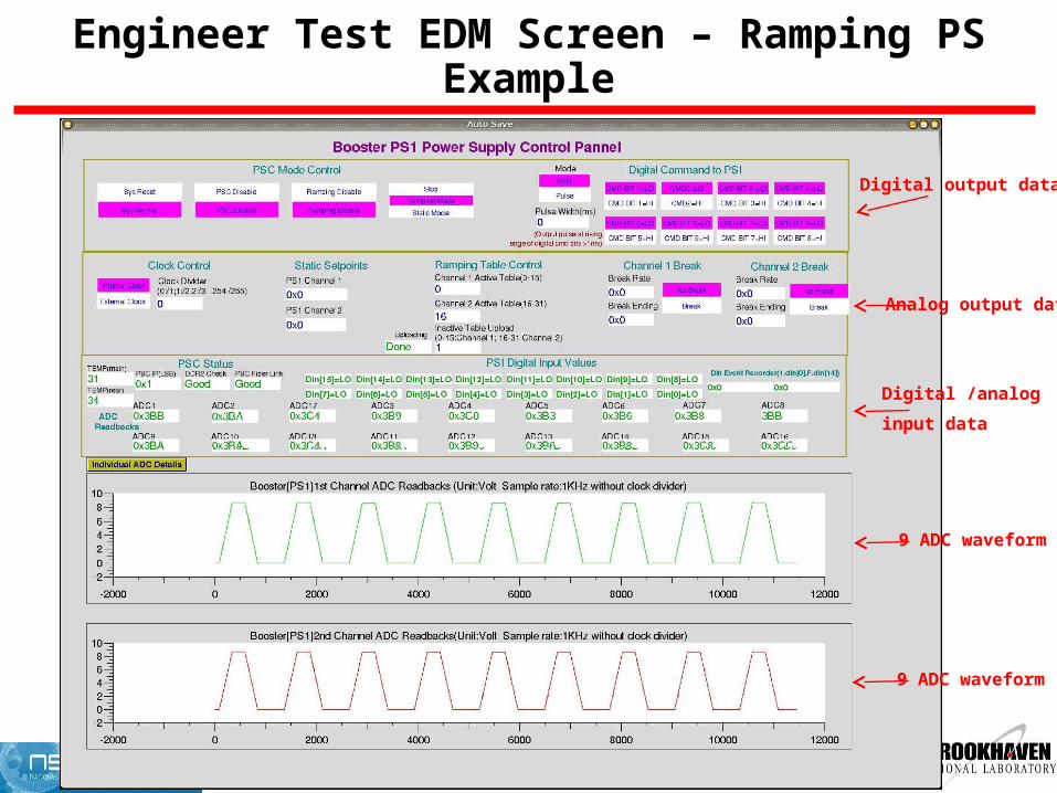
Engineer Test EDM Screen – Ramping PS Example
Digital output data
Analog output data
Digital /analog
input data
9 ADC waveform
9 ADC waveform

EPICS Collaboration Meeting, Hsinchu, Taiwan, June, 2011
Engineer Test EDM Screen – Ramping PS Example
1.1 second ADC waveform
(10KHz)
ADC channel selection
Ramping marker
(also shown on oscilloscope)

EPICS Collaboration Meeting, Hsinchu, Taiwan, June, 2011
Engineer Test EDM Screen – ADC Noise Measurement
ADC readback
(single channel chip)
Peak-peak: 1mv
(LSB=0.3mV)
ADC readback
(6channel chip)
Peak-peak: 2mv
(LSB=0.3mV)

EPICS Collaboration Meeting, Hsinchu, Taiwan, June, 2011
Device Support and Start Up Script

EPICS Collaboration Meeting, Hsinchu, Taiwan, June, 2011
Move Data Between EPICS IOC and FPGA Device
EPICS IOC
Small Data BulkRx Data BulkTx Data
(ai,ao,di,do etc)
BPM: gain, calbration BPM: filter coefficients BPM: TBT, ADC raw
CC: matrix selection CC: reverse response matrix CC: 10KHz orbit data
PSC: setpoints, commands PSC: Booster ramping function PSC: ADC readbacks
CA Client
(Physics applications)
Channel Access
FPGA (microBlaze / Xilkernel / LWIP TCP/IP)
TCP/IP
registers BRAM MPMC DDR2/DDR3
How do we design a simple/reliable protocol to transfer data between IOC /FPGA quickly ?

EPICS Collaboration Meeting, Hsinchu, Taiwan, June, 2011
General IOC-FPGA Communication Protocol
EPICS IOC
Small Data BulkRx Data BulkTx Data
(ai,ao,di,do etc)
Out: Combined small data into
one MTU by using aSub.
In: parse one MTU into small
data. Asyn Record Asyn RecordLarge amount data
ID frame1MTU
(10Hz)
1MTU
(10Hz)
ID
frame
(optional)
Large amount data
asyn port 1:
drvAsynIPPortConfigure
(“NormalRxTx", "192.168.1.10:7 TCP",0,0,0)
asyn port 2:
drvAsynIPPortConfigure
(“BulkRx", "192.168.1.10:18 TCP",0,0,0)
asyn port 3:
drvAsynIPPortConfigure
(“BulkTx", "192.168.1.10:20 TCP",0,0,0)

EPICS Collaboration Meeting, Hsinchu, Taiwan, June, 2011
Hardware Level – PSC

EPICS Collaboration Meeting, Hsinchu, Taiwan, June, 2011
1 = JTAG connectors – Programming to FPGA and CPLD.
2 = RS232 port – Communication to PC for diagnostic and software development.
3 = DDR2 memory modules – PS diagnostic data, CPU memory.
4 = SDI connectors – Communication between PSC master (or cell controller) and PSC slaves.
5 = Fiber transceiver – Communication with PSI.
6 = Ethernet connector – Communication to EPICS IOC for PSC master.
7 = FPGA (Spartan3A)
8 = CPLD(8a) & SPI memory(8b) – Dual boot and remote programming functions.
7a1
2
3
4
5
6
8a
8b
7
Hardware Level – PSC

EPICS Collaboration Meeting, Hsinchu, Taiwan, June, 2011
Brocade FWS624 24-port
Switch (4 GigE + 20 10/100Mbps)
PSC chassis and 20 PSCs
GigE to Linux IOC’s private network card
Hardware Level – PSC and Switch

EPICS Collaboration Meeting, Hsinchu, Taiwan, June, 2011
Hardware Level – PSI

EPICS Collaboration Meeting, Hsinchu, Taiwan, June, 2011
Hardware Level – PSI
Fiber to PSC
2 DACs
(20bit, 1ppm resolution, 1ppm
linearity, 0.1ppm/C drift)

EPICS Collaboration Meeting, Hsinchu, Taiwan, June, 2011
NSLS-II power supply control system
Want it ? You got it.
NSLS-II power supply control system is a open source hardware.

EPICS Collaboration Meeting, Hsinchu, Taiwan, June, 2011
Summary
1. Accelerator power supply control is the common task for each laboratory. It has similar requirements, and thus the similar architectures.
2. NSLS-II power supply control system design is based on the experiences from both power supply group and control group.
3. All the NSLS-II power supply control hardwires are in production stage. FPGA firmware and EPICS driver/applications are being tested on Booster and storage ring magnets.
4. NSLS-II power supply control system is a open source hardware. The PCB design, FPGA firmware design, and the EPICS driver/application design are open to the community.