Embed Size (px)
Citation preview
2010 FALL MEETING of the AVS HUDSON MOHAWK CHAPTER
Thursday, Oct 28, 2010 3-7pm
General Electric Global Research Center
1 Research Circle Niskayuna, NY 12065
Conference room 4 and 5
Topical Areas Biomaterials Environmental S&T Magnetic Materials Manufacturing S&T Materials Characterization Materials Processing MEMS Microelectronic Materials Nanometer-Scale S&T Plasma S&T Surface Engineering Surface Science Thin Films Vacuum Technology
Contacts Managing Director 212-248-0200, ext. 222
Exhibition 212-248-0200, ext. 229
Finance 212-248-0200, ext. 224
Marketing/Meetings 530-896-0477
Member Services 212-248-0200, 221
Publications 919-361-2787
Short Courses 530-896-0477
Web/IT 212-248-0200, ext. 223
Officers President David G. Castner
President-Elect Angus A. Rockett
Past-President Gregory J. Exarhos
Secretary Joe Greene
Treasurer Stephen M. Rossnagel
Directors Alison A. Baski Jane P. Chang Steven M. George Luke Hinkle Graham Leggett Susan B. Sinnott
AVS 125 Maiden Lane, 15th Floor New York NY 10038
Phone: 212-248-0200 Fax: 212-248-0245 E-mail: [email protected] Web: www.avs.org
Talks T1. MAKING MOLECULAR MULTILAYERS USING “CLICK” CHEMISTRY: GROWTH AND THIN FILM CHARACTERIZATION, Peter K. B. Palomaki and Peter H. Dinolfo, Department of Chemistry & Chemical Biology and The Baruch ‘60 Center for Biochemical Solar Energy Research, Rensselaer Polytechnic Institute, 110 8th Street, Troy, NY 12180 T2. RAMAN STUDY OF INTERFACIAL LOAD TRANSFER IN GRAPHENE-POLYMER NANOCOMPSOITES, Iti Srivastava1, Linda Schadler1 and Nikhil Koratkar 2
1 Department of Material Science and Engineering, 2 Department of Mechanical, Aerospace and Nuclear Engineering,Rensselaer Polytechnic Institute, Troy, NY 12180, USA
T3. A NOVEL APPROACH TO CREATE VERTICALLY ALIGNED BIAXIAL TEXTURED TUNGSTEN NANORODS, Rahul Krishnan1 *, Yu Liu2, Churamani Gaire2, Liang Chen, Gwo-Ching Wang2 and Toh-Ming Lu2 1Department of Materials Science and Engineering, Rensselaer Polytechnic Institute, 110 8th St., Troy, NY 12180, USA, 2Department of Physics, Applied Physics and Astronomy, Rensselaer Polytechnic Institute, 110 8th St., Troy, NY 12180, USA
T4. REDUCTION KINETICS OF GRAPHENE OXIDE DETERMINED BY TEMPERATURE PROGRAMMED DESORPTION Carl A. Ventrice, Jr1, Daniel A. Field2, Nicholas J. Clark2, Heike Geisler3, Inhwa Jung4, Dongxing Yang4, Richard Piner4, and Rodney S. Ruoff4 1College of Nanoscale Science & Engineering, University at Albany, Albany, NY 12203, 2Department of Physics, Texas State University, San Marcos, TX 78666, 3Inst. for Environmental & Industrial Sci., Texas State University, San Marcos, TX 78666 T5. CAPACITANCE-VOLTAGE (C-V) AND X-RAY PHOTOELECTRON SPECTROSCOPY (XPS) STUDY OF THE EFFECT OF A La2O3 LAYER IN THE TiN/HfO2/SiO2/p-Si STACK, *E. Bersch, *M. Di, **S. Consiglio, **R.D. Clark, **G.J. Leusink, and *A.C. Diebold, *College of Nanoscale Science and Engineering, University at Albany, 255 Fuller Rd., Albany, NY 12203, **TEL Technology Center, America, LLC, 255 Fuller Rd., Albany, NY 12203 T6. ToF-SIMS DEPTH PROFILES OF ENZYMATICALLY DEGRADED POLY(PEPTIDE URETHANEUREAS), Gilad Zorn1, Felix I. Simonovsky2, Jeremy Brison1, Shin Muranoto1, Buddy D. Ratner1 2, David G. Castner1 2 , National ESCA and Surface Analysis Center for Biomedical Problems, 1Department of Chemical Engineering and 2Department of Bioengineering, University of Washington, Seattle, WA 98195-1750.
Posters
P1. METAL-DIELECTRIC INTERFACE TOUGHENING BY CERAMIZATION OF A MOLECULAR NANOLAYER AND ITS CHARACTERIZATION AT A BURIED INTERFACE, Saurabh Garg1, Ranganath Teki1, Ashutosh Jain1, K. Chinnathambi1, Binay Singh1, V. S. Smentkowski3, Michael Lane2, Ganpati Ramanath1
1 Materials Science & Engineering Department, Rensselaer Polytechnic Institute, Troy, NY 12180. 2Department of Chemistry, Emory and Henry College, Emory, VA 24237, 3General Electric Global Research Center, Niskayuna, NY
P2. KINETICS OF TITANIA NANOTUBE FORMATION BY ANODIZATION OF TITANIUM FILMS, Gorun Butail, P. G. Ganesan, M. Raddiar, R. Teki, N. Ravishankar, D. J. Duquette, Ganpati Ramanath, Department of Materials Science and Engineering, Rensselaer Polytechnic Institute.
P3. THE EFFECT OF HUMIDITY ON COPPER-SILICA INTERFACE FRACTURE TOUGHNESS, Dandapani Vijayashankar1, Ranganath Teki1, Saurabh Garg1, Ashutosh Jain1, Michael Lane2, Hong Zhu3, Rampi Ramprasad3 and Ganpati Ramanath1
1Rensselaer Polytechnic Institute, Materials Sci. and Engg. Dept., Troy, NY, 12180, USA 2Emory and Henry College, Chemistry Department, Emory, VA 24327, USA 3University of Connecticut, Materials Science and Engineering Department, Storrs, CT P4. LARGE AREA CROSS SECTIONAL MICROSTRUCTURAL CHARACTERIZATION OF TOF-SIMS DEPTH PROFILE CRATERS, V.S. Smentkowski* and D. Ellis, General Electric Global Research Center
P5. MULTIVARIATE STATISTICAL ANALYSIS OF 3 DIMENSIONAL McS+ TIME OF FLIGHT SECONDARY ION MASS SPECTROMETRY DATA, Vincent S. Smentkowski1, Mike Keenan2, 1General Electric Global Research Center, 1 River Road, Niskayuna NY 12309, 28346 Roney Road, Wolcott, NY 14590
P6. DIRECTED RAPID SYNTHESIS AND BULK ASSEMBLY OF SCULPTED NANOCRYSTALS WITH TAILORED PROPERTIES FOR THERMOELECTRIC ENERGY CONVERSION, Rutvik J Mehta1,§, Yanliang Zhang2, Priyanka Jood1, C. Karthik1, Binay Singh1, Wei Jiang1, , Theo Borca-Tasciuc2 and Ganpati Ramanath1,
1Materials Science and Engineering Department, 2Mechanical Engineering Department Rensselaer Polytechnic Institute, 110 8th St. Troy, NY 12180, USA P7. MORPHOLOGY AND TEXTURE EVOLUTION OF NANOSTRUCTURED CaF2 FILMS ON AMORPHOUS SUBSTRATES UNDER OBLIQUE INCIDENCE FLUX C. Gaire, P. Snow, T.-L. Chan, S. B. Zhang, G.-C. Wang, and T.-M. Lu, Department of Physics, Applied Physics and Astronomy, Rensselaer Polytechnic Institute, 110 8th Street, Troy, NY, 12180-3590
P8. ELECTROCHEMICAL SYNTHESIS AND CHARACTERIZATION OF HIGH-FILLING COPPER NANOWIRE ARRAYS INTO PAAM TEMPLATES, Nan Li, Brian Willis, Department of Chemical, Materials and Biomolecular Engineering, University of Connecticut, Storrs, CT P9. OPTICAL PROPERTIES OF POLYCRYSTALLINE CHEMICAL VAPOR DEPOSITED (CVD) GRAPHENE GROWN ON COPPER FOILS INVESTIGATED WITH SPECTROSCOPIC ELLIPSOMETRY (SE), F. Nelson, 1 V. Kamineni,1 T. Zhang, 1 E. Comfort, 1 J. Lee, 1 A. C. Diebold1 1College of Nanoscale Science and Engineering
P10. ADVANCED CHARACTERIZATION METHODS FOR CdTe/CdS/TCO INTERFACES *L. Le Tarte, A. Barbuto, J. Cournoyer, K. Dovidenko, D. Ellis, R. Neander, V. Smentkowski, **B. Lita, M.J. Pavol, *General Electric, Global Research Center, Niskayuna, NY 12309 **PrimeStar Solar, Arvada, CO 80004 P11. NEW POSSIBILITIES IN HIGH SENSITIVITY LOW ENERGY ION SCATTERING (LEIS) FOR PROBING THE OUTERMOST ATOMIC LAYER, A. Schnieders1,2, Thomas Grehl3, Philipp Brüner3, Hidde Brongersma3,4, Michael Fartmann4, Rik ter Veen4 N. Havercroft2 , 1 Tascon USA, Inc., 100 Red Schoolhouse Road, Chestnut Ridge, NY 10977, USA, 2 ION-TOF USA, Inc., 100 Red Schoolhouse Road, Chestnut Ridge, NY 10977, USA, 3 ION-TOF GmbH, Heisenbergstr. 15, 48149 Muenster, Germany, 4 Tascon GmbH, Heisenbergstr. 15, 48149 Muenster, Germany
P12. METROLOGY AND MANIPULATION OF HEAT TRANSPORT AT METAL-DIELECTRIC INTERFACES, Peter O’Brien1, Jianxun Liu2, Ranganath Teki1, Masashi Yamaguchi2, Pawel Keblinski1, Ganpati Ramanath1, 1 Department of Materials Science and Engineering, and, 2 Department of Physics, Rensselaer Polytechnic Institute, Troy, NY.
P13. NANOSCALE ELECTRON EMITTER LIFETIME: THE ROLE OF HEAT CONDUCTION, J. Scott Price, GE Global Research, 1 Research Circle, Niskayuna, NY 12309
P14. VISUALIZE THE EXTRUSION AND VOIDS INDUCED IN COPPER-FILLED THROUGH-SILICON VIAS (TSVS) AT VARIOUS TEMPERATURES USING X-RAY MICROSCOPY, LayWai Kong1, Andrew C. Rudack2, Peter Krueger3, Ehrenfried Zschech3, Sitaram Arkalgud2, A.C. Diebold1 , College of Nanoscale Science and Engineering, University at Albany, Albany, N.Y. 122031, SEMATECH, Albany, N.Y. 122032 Fraunhofer Institute for Nondestructive Testing (IZFP), Dresden, Germany3, 255 Fuller Road 12203 Albany, NY
P15. MODELING THE IMPACT OF COPPER PLASTICITY ON THERMO-MECHANICAL STRESS INDUCED BY THROUGH-SILICON VIAS (TSVS), Ben Backes1, Colin McDonough1, Jihan Capulong1, Larry Smith2, Tom Jing1, Robert Geer1, and Wei Wang1
1 College of Nanoscale Science and Engineering, University at Albany, Albany, NY, 12203, 2 SEMATECH, Albany, NY 12203
P16. NANOSCALE FABRICATION AND CHARACTERIZATION FOR MATERIALS FOR BEYOND-CMOS DEVICES Prabhu Balasubramanian1, Delia Bearup1*, Adam Bross1, See Wee Chee1, Jeremey Graham2, Li He1, Jessica Murphy1*, Hamed Parvaneh1, Xiaowei Wu1 and Robert Hull11. Dept. of Materials Science and Engineering, Rensselaer Polytechnic Institute (*Now graduated) 2. Dept. of Engineering Physics, University of Virginia P17. MAKING MOLECULAR MULTILAYERS USING “CLICK” CHEMISTRY: GROWTH AND THIN FILM CHARACTERIZATION, Peter K. B. Palomaki and Peter H. Dinolfo, Department of Chemistry & Chemical Biology and The Baruch ‘60 Center for Biochemical Solar Energy Research, Rensselaer Polytechnic Institute, 110 8th Street, Troy, NY 12180 P18. MODELLING ION PATH ABOVE THE ELECTRODE WITH BIASED GRID, Jozef Brcka, TEL US Holdings, Inc., Technology Development Center, 255 Fuller Rd., Albany, NY 12203

Talks

MAKING MOLECULAR MULTILAYERS USING “CLICK” CHEMISTRY: GROWTH AND THIN FILM CHARACTERIZATION
Peter K. B. Palomaki and Peter H. Dinolfo
Department of Chemistry & Chemical Biology and The Baruch ‘60 Center for Biochemical
Solar Energy Research Rensselaer Polytechnic Institute, 110 8th Street, Troy, NY 12180
Email: [email protected]
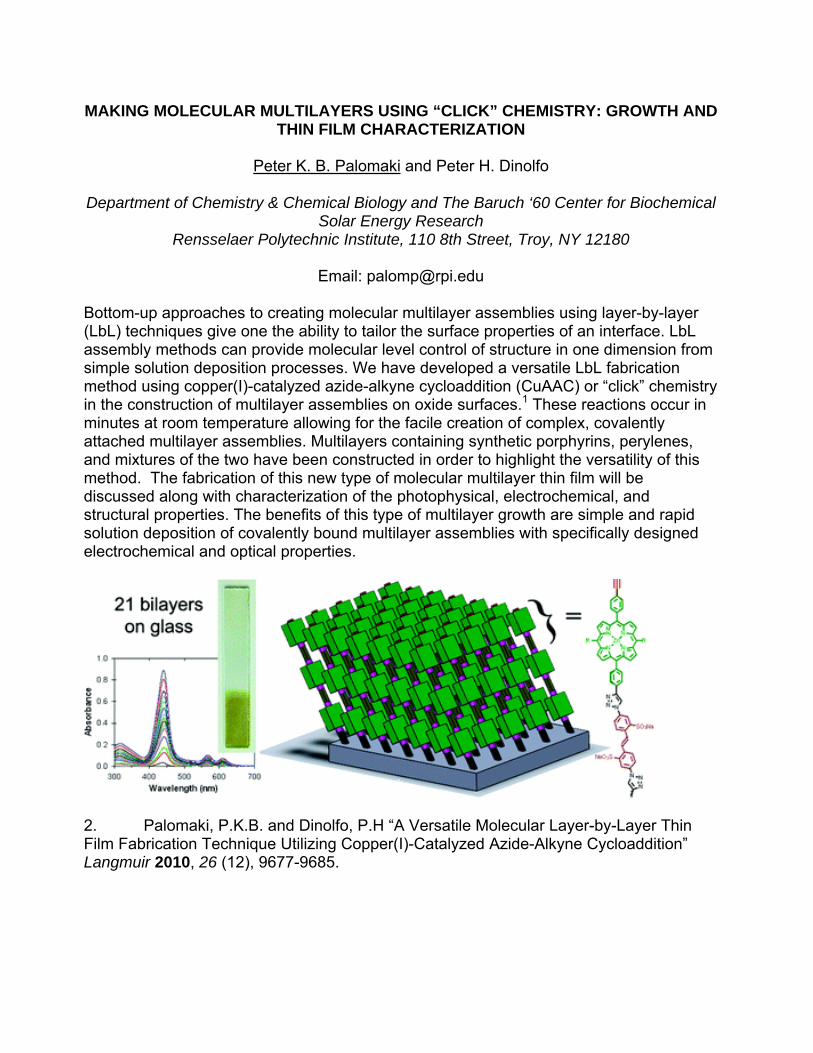
Bottom-up approaches to creating molecular multilayer assemblies using layer-by-layer (LbL) techniques give one the ability to tailor the surface properties of an interface. LbL assembly methods can provide molecular level control of structure in one dimension from simple solution deposition processes. We have developed a versatile LbL fabrication method using copper(I)-catalyzed azide-alkyne cycloaddition (CuAAC) or “click” chemistry in the construction of multilayer assemblies on oxide surfaces.1 These reactions occur in minutes at room temperature allowing for the facile creation of complex, covalently attached multilayer assemblies. Multilayers containing synthetic porphyrins, perylenes, and mixtures of the two have been constructed in order to highlight the versatility of this method. The fabrication of this new type of molecular multilayer thin film will be discussed along with characterization of the photophysical, electrochemical, and structural properties. The benefits of this type of multilayer growth are simple and rapid solution deposition of covalently bound multilayer assemblies with specifically designed electrochemical and optical properties.
1. Palomaki, P.K.B. and Dinolfo, P.H “A Versatile Molecular Layer-by-Layer Thin Film Fabrication Technique Utilizing Copper(I)-Catalyzed Azide-Alkyne Cycloaddition” Langmuir 2010, 26 (12), 9677-9685.
RAMAN STUDY OF INTERFACIAL LOAD TRANSFER IN GRAPHENE-POLYMER NANOCOMPSOITES
Iti Srivastava1, Linda Schadler1 and Nikhil Koratkar 2
1 Department of Material Science and Engineering 2 Department of Mechanical, Aerospace and Nuclear Engineering,
Rensselaer Polytechnic Institute, Troy, NY 12180, USA
Characteristic Raman band shifts have proven to be a valuable technique to study load transfer mechanisms in polymer nanocomposites. The stress transfer to the reinforcing filler imposes elastic strains in the filler materials, proportionally shifting their characteristic Raman bands. Tracking the strain-sensitive filler Raman band shifts with respect to the stress state applied to the nanocomposite reveals insights regarding the filler-matrix interactions at the micro-mechanical level, which we used to probe the extent of graphene-polymer interfacial interactions and determine the basis for strengthening. In our previous work, we have demonstrated greatly improved mechanical properties in polymer nanocomposites using small quantities (<0.1 wt. %) of graphene platelets. We relate the macroscopic mechanical behavior to the nanoscopic mechanisms at the interface by studying the strain-induced Raman bands shifts in these nanocomposites. We tracked the strain-sensitive characteristic Raman G-band shift of graphene platelets in poly-dimethyl-siloxane nanocomposites. We obtained large debonding strains of ~7% for graphene in PDMS, with the peak shift rate with strain being ~2.4 cm-1/composite strain% in comparison to single walled carbon nanotube composites, where a relatively low rate of ~0.1 cm-1/composite strain% was obtained, suggesting enhanced load-transfer effectiveness for graphene. A surprising observation was that for large strains (>1.5%) the graphene fillers went into compression under uniaxial tensile deformation and vice versa. This effect is related to the high mobility of the poly-dimethyl-siloxane chains at room temperature. We performed thermo-mechanical experiments, where an increase in the glass transition temperature by 10 deg C the nanocomposite verified the strong bonding between graphene platelets and polymer matrix. We also utilize atomic force microscopy to unravel the interphase between graphene and epoxy. These insights of the stress transfer mechanism would enable rational design of strategies to circumvent existing failure mechanisms through graphene-polymer interfacial engineering.
A NOVEL APPROACH TO CREATE VERTICALLY ALIGNED BIAXIAL TEXTURED TUNGSTEN NANORODS
Rahul Krishnan1 *, Yu Liu2, Churamani Gaire2, Liang Chen, Gwo-Ching Wang2 and Toh-
Ming Lu2 1Department of Materials Science and Engineering, Rensselaer Polytechnic Institute, 110
8th St., Troy, NY 12180, USA 2Department of Physics, Applied Physics and Astronomy, Rensselaer Polytechnic
Institute, 110 8th St., Troy, NY 12180, USA *Correspondence: [email protected]
Recently there has been keen interest in creating biaxial metal or dielectric films as a substrate for further growth of functional materials such as high Tc superconductors and semiconductors. Oblique angle deposition is one convenient approach to grow biaxial films. However, so far for oblique angle deposition of biaxial metal films, often the out-of-plane crystal orientation is not normal to the substrate but with an angle leaning towards the incident flux. Here we report vertical biaxial textured tungsten nanorods (A15 crystal structure) that have been grown by oblique angle (α = 85º from the surface normal) DC magnetron sputtering using a novel substrate rotation mode called ‘two-step rotation’ [1]. In this mode, the substrate is given a fast rotation through 180˚ at 90 rpm followed by a rest period of 30 seconds. As a result of this rotation mode, the flux is incident from two diametrically opposite directions on the sample at an oblique angle, averaging out the growth into vertical columns that retain the in-plane texture. These nanorods of thickness ~390 nm have a [002] out-of-plane orientation along with a [11̄ 0] in-plane texture as shown by X-ray pole figure analysis. The in-plane texture is selected so as to obtain maximum capture area. In contrast, the tungsten nanorods of thickness ~390 nm obtained without substrate rotation are slanted with an angle of ~45˚ towards the flux. In this case, the [002] texture axis is tilted ~17˚ away from the substrate normal (towards the flux) and the selection of a [03̄ 1] in-plane texture does not maintain maximum in-plane capture area. The vertical nanorods with different thicknesses (10 nm, 25 nm, 50 nm and 100 nm) were also grown and analyzed for biaxial texture evolution using a highly surface sensitive Reflection High-Energy Electron Diffraction (RHEED) pole figure technique [2, 3]. The initial polycrystalline film begins to show the inception of biaxial texture with a fiber background between 10 and 25 nm. Biaxial texture development is eventually completed between 50 and 100 nm thicknesses of the film. Scanning Electron Microscopy and Atomic Force Microscopy show that the vertical tungsten nanorods have a (112) crystal habit which is a minimum surface energy plane for the cubic A15 crystal structure. References [1] R. Krishnan, T. Parker, S. Lee and T-M. Lu, Nanotechnology, 20, 465609, 2009 [2] R. Krishnan, Y. Liu, C. Gaire, L. Chen, G-C. Wang and T-M. Lu, Nanotechnology, 21, 325704, 2010 [3] F. Tang, T. Parker, G-C. Wang and T-M. Lu, J. Phys. D: Appl. Phys., 40, p R427, 2007
REDUCTION KINETICS OF GRAPHENE OXIDE DETERMINED BY TEMPERATURE PROGRAMMED DESORPTION
Carl A. Ventrice, Jr1, Daniel A. Field2, Nicholas J. Clark2, Heike Geisler3, Inhwa Jung4,
Dongxing Yang4, Richard Piner4, and Rodney S. Ruoff4
1College of Nanoscale Science & Engineering, University at Albany, Albany, NY 12203 2Department of Physics, Texas State University, San Marcos, TX 78666
3Inst. for Environmental & Industrial Sci., Texas State University, San Marcos, TX 78666 4Department of Mechanical Engineering, University of Texas, Austin, TX 78712
Email: [email protected]
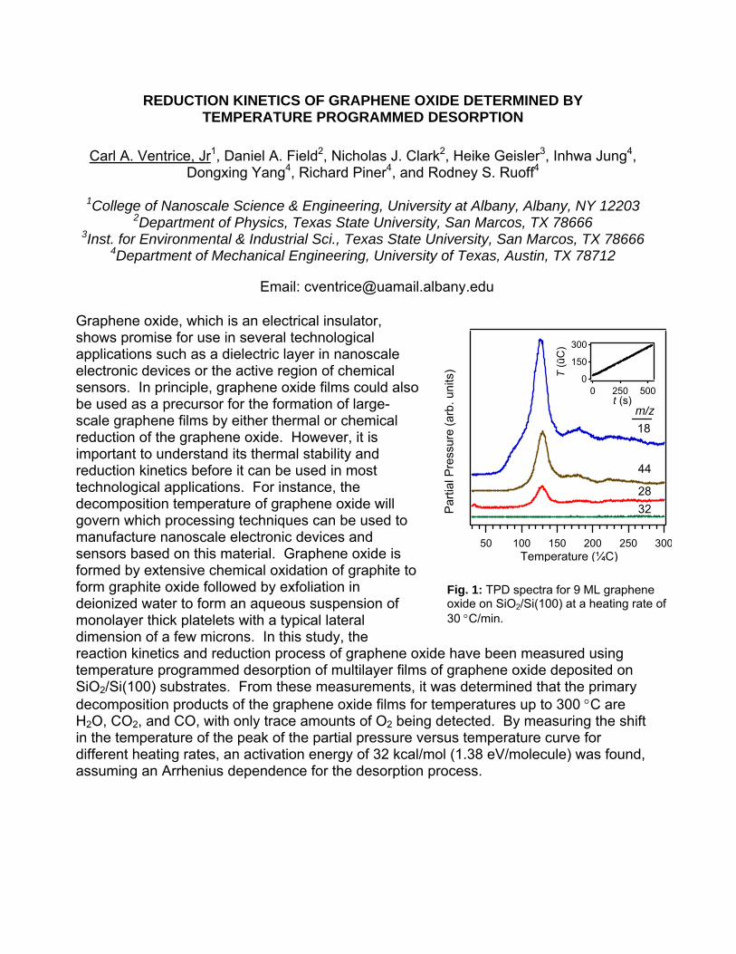
Graphene oxide, which is an electrical insulator, shows promise for use in several technological applications such as a dielectric layer in nanoscale electronic devices or the active region of chemical sensors. In principle, graphene oxide films could also be used as a precursor for the formation of large-scale graphene films by either thermal or chemical reduction of the graphene oxide. However, it is important to understand its thermal stability and reduction kinetics before it can be used in most technological applications. For instance, the decomposition temperature of graphene oxide will govern which processing techniques can be used to manufacture nanoscale electronic devices and sensors based on this material. Graphene oxide is formed by extensive chemical oxidation of graphite to form graphite oxide followed by exfoliation in deionized water to form an aqueous suspension of monolayer thick platelets with a typical lateral dimension of a few microns. In this study, the reaction kinetics and reduction process of graphene oxide have been measured using temperature programmed desorption of multilayer films of graphene oxide deposited on SiO2/Si(100) substrates. From these measurements, it was determined that the primary decomposition products of the graphene oxide films for temperatures up to 300 C are H2O, CO2, and CO, with only trace amounts of O2 being detected. By measuring the shift in the temperature of the peak of the partial pressure versus temperature curve for different heating rates, an activation energy of 32 kcal/mol (1.38 eV/molecule) was found, assuming an Arrhenius dependence for the desorption process.
Par
tial P
ress
ure
(arb
. un
its)
30025020015010050Temperature (¼C)
m/z
18
44
28
32
300
150
0T (ūC
)
5002500t (s)
Fig. 1: TPD spectra for 9 ML graphene oxide on SiO2/Si(100) at a heating rate of 30 C/min.
CAPACITANCE-VOLTAGE (C-V) AND X-RAY PHOTOELECTRON SPECTROSCOPY (XPS) STUDY OF THE EFFECT OF A La2O3 LAYER IN THE TiN/HfO2/SiO2/p-Si
STACK
*E. Bersch, *M. Di, **S. Consiglio, **R.D. Clark, **G.J. Leusink, and *A.C. Diebold
*College of Nanoscale Science and Engineering, University at Albany, 255 Fuller Rd., Albany, NY 12203
**TEL Technology Center, America, LLC, 255 Fuller Rd., Albany, NY 12203
There has been much attention paid recently to the lowering of the threshold voltage (Vt) that is
accomplished by including an additional ultrathin (~5-10 Å) oxide layer in the high-k/metal gate
metal oxide semiconductor field effect transistor (MOSFET) gate stack. We have investigated the
TiN/HfO2/La2O3/SiO2/p-Si stack, where the La2O3 layer is the so-called Vt-shift layer. For several
variations of this stack, where both the thickness and the position of the La2O3 layer were
systematically varied, we measured two quantities directly related to the Vt, the flatband voltage
(Vfb) and the Si band bending. The Vfb was measured using capacitance-voltage (C-V)
measurements on stacks with 500 Å TiN layers, and the Si band bending was measured on sister
wafers with 30 Å TiN layers. For a set of samples where the thickness of the La2O3 between the
HfO2 and SiO2 layers was varied, we observed that the Vfb and Si band bending both become more
negative as the thickness of the La2O3 was increased. For a set of samples where position of the
La2O3 within the HfO2 layer was varied, we observed that the Vfb and Si band bending became less
negative as the amount of HfO2 between the La2O3 and the SiO2 was increased. These
observations support the proposition that there is a dipole at the La2O3/SiO2 interface which affects
the Si band bending, as has been reported in the literature.1,2 We have also observed that there is a
difference in the Vfb and Si band bending in TiN/HfO2/La2O3/SiO2/p-Si stacks with thermally
grown and chemically grown SiO2 layers. Results of this study as well as one where the thickness
of thermally grown SiO2 layers was varied will be presented, and it implications on the theory of
the interface dipole with be discussed.
1. K. Kita, et al., Appl. Phys. Lett, 94, 132902 (2009).
2. P.D. Kirsch, et al., Appl. Phys. Lett., 92, 092901 (2008).
ToF-SIMS DEPTH PROFILES OF ENZYMATICALLY DEGRADED POLY(PEPTIDE URETHANEUREAS)
Gilad Zorn1, Felix I. Simonovsky2, Jeremy Brison1, Shin Muranoto1,
Buddy D. Ratner1 2, David G. Castner1 2
National ESCA and Surface Analysis Center for Biomedical Problems 1Department of Chemical Engineering and 2Department of Bioengineering
University of Washington, Seattle, WA 98195-1750.
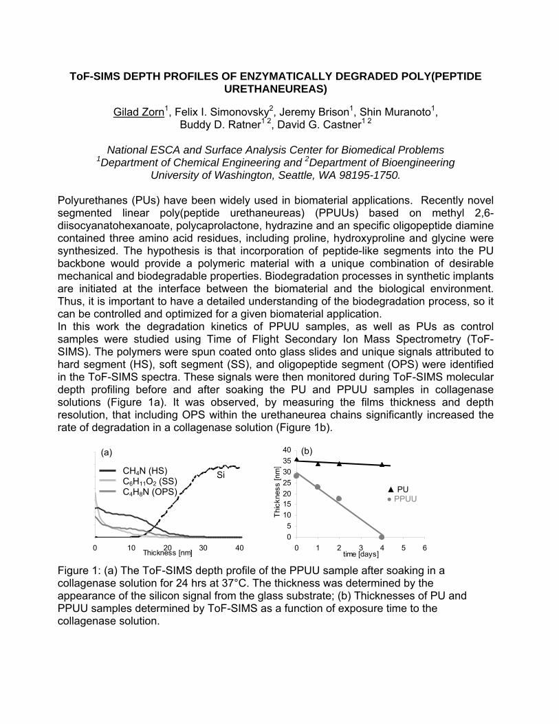
Polyurethanes (PUs) have been widely used in biomaterial applications. Recently novel segmented linear poly(peptide urethaneureas) (PPUUs) based on methyl 2,6-diisocyanatohexanoate, polycaprolactone, hydrazine and an specific oligopeptide diamine contained three amino acid residues, including proline, hydroxyproline and glycine were synthesized. The hypothesis is that incorporation of peptide-like segments into the PU backbone would provide a polymeric material with a unique combination of desirable mechanical and biodegradable properties. Biodegradation processes in synthetic implants are initiated at the interface between the biomaterial and the biological environment. Thus, it is important to have a detailed understanding of the biodegradation process, so it can be controlled and optimized for a given biomaterial application. In this work the degradation kinetics of PPUU samples, as well as PUs as control samples were studied using Time of Flight Secondary Ion Mass Spectrometry (ToF-SIMS). The polymers were spun coated onto glass slides and unique signals attributed to hard segment (HS), soft segment (SS), and oligopeptide segment (OPS) were identified in the ToF-SIMS spectra. These signals were then monitored during ToF-SIMS molecular depth profiling before and after soaking the PU and PPUU samples in collagenase solutions (Figure 1a). It was observed, by measuring the films thickness and depth resolution, that including OPS within the urethaneurea chains significantly increased the rate of degradation in a collagenase solution (Figure 1b). Figure 1: (a) The ToF-SIMS depth profile of the PPUU sample after soaking in a collagenase solution for 24 hrs at 37°C. The thickness was determined by the appearance of the silicon signal from the glass substrate; (b) Thicknesses of PU and PPUU samples determined by ToF-SIMS as a function of exposure time to the collagenase solution.
0 10 20 30 40Thickness [nm]
SiCH4N (HS) C6H11O2 (SS) C4H8N (OPS)
(a)
0
5
10
1520
25
30
35
40
0 1 2 3 4 5 6time [days]
Thi
ckne
ss [n
m]
▲ PU ● PPUU
(b)

Posters
METAL-DIELECTRIC INTERFACE TOUGHENING BY CERAMIZATION OF A MOLECULAR NANOLAYER AND ITS CHARACTERIZATION AT A BURIED
INTERFACE
Saurabh Garg1, Ranganath Teki1, Ashutosh Jain1, K. Chinnathambi1, Binay Singh1, V. S. Smentkowski3, Michael Lane2, Ganpati Ramanath1
1 Materials Science & Engineering Department, Rensselaer Polytechnic Institute, Troy, NY 12180.
2Department of Chemistry, Emory and Henry College, Emory, VA 24237
3General Electric Global Research Center, Niskayuna, NY
Integration of metal-dielectric interfaces using molecular nanolayers (MNLs) is attractive for prospective applications such as laminates in high frequency electronics and packaging, nanodevice wiring and composites. Recent works have shown that annealing-induced siloxane bridging can toughen organosilane-functionalized copper-silica interfaces. While strong bonding of the MNL with the under- and over-layers is essential for promoting adhesion, the nature of the MNL structure and bonding, especially at temperatures where the MNLs are known to degrade on bare surfaces, are unclear. But tracking atomic-level intermixing and interfacial phase formation in a sub-nm-layer is an exacting challenge due to difficulties in distinguishing Si atoms in the organosilane MNL from Si atoms in the silica substrate, and obtaining sufficient contrast by electron microscopy. Here, we study organogermane-tailored interfaces using a combination of electron spectroscopy and microscopy, and density functional theory calculations to obtain insights into the interface chemical changes. Our results reveal that annealing decomposes the organic monolayer into an inorganic network, leading to interface toughening. We assembled Benzyl-trichlorogermane (BTCG) on silica to form a 0.7-nm-thick nanolayer. Four-point bending fracture tests on as-prepared Cu/BTCG/SiO2 sandwiches revealed a low interface toughness of 2.1 J/m2, comparable to pristine Cu/SiO2 structures. However, interfacial toughness increased monotonically with annealing temperature, yielding values as high as 23.3 J/m2 for Tanneal = 500 ºC. Core-level spectra from silica fracture surfaces show a strong Ge signature for Tanneal ≤ 300 ºC that becomes undetectable for Tanneal ≥ 400 ºC, suggesting Ge transport and destruction of the organic MNL. This result is corroborated by time-of-flight secondary ion mass spectroscopy (SIMS) profiles showing the smearing of the interfacial Ge spike into the silica layer upon annealing. Incorporation of Ge in the silica weakens the Si-O-Si network, leading to intermixing of Si, O and Cu, forming nanoscale islands of rhobohedral CuSiO3 observable by cross-sectional transmission electron microscopy and X-ray spectroscopy. For pristine Cu/SiO2 structures there were no changes at the interface and the toughness value was ~ 3 J/m2 for Tanneal ≤ 700 °C. Our findings suggest that molecular degradation of the organic MNL to form nanoscopic layer of inorganic metal-oxide-silicon bonds could be an attractive approach for toughening interfaces.
KINETICS OF TITANIA NANOTUBE FORMATION BY ANODIZATION OF TITANIUM FILMS
Gorun Butail, P. G. Ganesan, M. Raddiar, R. Teki, N. Ravishankar, D. J. Duquette,
Ganpati Ramanath
Department of Materials Science and Engineering, Rensselaer Polytechnic Institute.
[email protected], 646-717-3921.
Titania is a promising photocatalyst used in a variety of photovoltaic, optoelectronic and biofiltering applications. Inexpensive synthesis of high surface area titania nanostructures are attractive for high-efficiency low-cost application because of unidirectional charge transport and low scattering losses. Investigation as well understanding the growth mechanism of these titania nanostructures will help us in efficient application and synthesis of titania nanostructures. Here we investigate a low-cost electrochemical synthesis technique to controllably obtain nanoporous titania films with vertically aligned nanotube arrays and elucidate, for the first time, the key kinetic processes and mechanisms of nanotube formation. Titania nanotubes were formed by anodizing titanium films in a mixture of ethylene glycol and ammonium fluoride at chosen temperatures and potentials between 30 and 80 °C and 30 and 80 V, respectively. Cross-sectional and plan-view electron microscopy and X-ray spectroscopy reveal the formation of ordered arrays of titania nanotubes. Our results show that the nanotube length increase is thermally activated, and governed by voltage-dependent activation energy 0.6 eV Eeff 1.1 eV expressed by Eeff E0 Vanod where is a constant and E0 = 1.6 eV is a voltage-
independent term. The proximity of E0 to that of oxygen diffusion in titania suggests that oxygen transport across the titania walls at the pore bottoms is the rate-limiting step. These results provide insights into the mechanism of titania nanotube formation and a framework for their rational synthesis for applications.
THE EFFECT OF HUMIDITY ON COPPER-SILICA INTERFACE FRACTURE TOUGHNESS
Dandapani Vijayashankar1, Ranganath Teki1, Saurabh Garg1, Ashutosh Jain1, Michael
Lane2, Hong Zhu3, Rampi Ramprasad3 and Ganpati Ramanath1
1Rensselaer Polytechnic Institute, Materials Sci. and Engg. Dept., Troy, NY, 12180, USA 2Emory and Henry College, Chemistry Department, Emory, VA 24327, USA
3University of Connecticut, Materials Science and Engineering Department, Storrs, CT email: [email protected] The fracture toughness (ΓFT) of metal-ceramic interfaces is often determined by the nature of interfacial bonding between the metal and the surface group on the ceramic. The role of humidity in copper-silica interfacial adhesion, i.e. on Cu-O-Si bonding, is of great interest to tailoring durable high-performance interfaces in nanodevice wiring and packaging, and high frequency communication devices. Here, we demonstrate that the room-temperature toughness of copper-silica interfaces is a strong function of humidity. We have studied the effect of moisture on the toughness of Cu/SiO2 and Au/SiO2
interfaces and the role of humidity as a tool in partitioning ΓFT of metal-ceramic interfaces. We also performed density functional theory calculations to understand the energetics of bond-breaking processes happening at the crack tip. Thin film sandwich structures were made by the deposition of Cu or Au on Si (001) wafers with an 85-nm thick thermal silica layer and tested on a four point bend test system in a temperature- and humidity-controlled environment. Our results reveal that increasing water activity aH2O from 0.05 to 0.8 at 323 K results in a three-fold decrease in ΓFT for the
Cu-silica interface from 5.4 to 1.8 J/m2. We attribute this decrease to water-induced Cu-O-Si interfacial bond breaking, similar to stress corrosion cracking in bulk silica glasses. Our results on gold, which does not form a native oxide under ambient conditions, show that the gold-silica interfacial toughness remains constant at 0.5 ± 0.1 J/m2. Examination of the bond free energies reveals that the Cu-O bond needs a lower external stress to break via hydrolysis as compared to the Si-O bond, which is supported by density functional theory calculations. This framework can be adapted to study the effects of environmental degradation in a wide variety of interfacial applications ranging from microelectronics to biological implants through an appropriate choice of chemical environments.
LARGE AREA CROSS SECTIONAL MICROSTRUCTURAL CHARACTERIZATION OF TOF-SIMS DEPTH PROFILE CRATERS
V.S. Smentkowski* and D. Ellis
General Electric Global Research Center
1 River Road Niskayuna NY 12309 *[email protected]
Focused Ion Beam (FIB) techniques [1] are widely used in order to generate cross sections of samples which can then be analyzed using a variety of analytical instrumentation in order to obtain microstructural information. In order to rapidly generate FIB cross sections, small areas (typically 5 to 10 microns) are milled. Time of Flight Secondary Ion Mass Spectrometry (ToF-SIMS) is a powerful surface analytical technique that is able to measure low concentrations of sub surface species [2]. ToF-SIMS depth profile measurements are collected by eroding a large area (50 to 1,000 microns in size) of a sample using an ion beam for a certain amount of time, pausing the erosion, analyzing a smaller (central) region of the eroded area, and repeating the cycle until the desire depth has been reached. Ion images are often recorded at each depth and a full mass spectrum is saved at every volume element allowing for 3 D analysis [3]. Often times, both ToF-SIMS depth profile analysis and high resolution microstructural SEM characterization are required on the same sample. Ideally, these complimentary analyses would be performed in the same region of a sample. In this presentation, we will demonstrate that FIB techniques can be used to clean up the large area craters produced by ToF-SIMS depth profile analysis thereby enabling microstructural characterization over larger areas of samples. Advantages of this approach are: larger FIB cross sections can be prepared since a significant amount of material was removed during the erosion cycles in the ToF-SIMS analysis, combining the chemical information provided from the ToF-SIMS analysis with the large area microstructural characterization provided by FIB-SEM analysis, and having both the ToF-SIMS and the large area cross sectional analysis performed in the same region of the sample. The ToF-SIMS depth profile craters have a slope of about 45 deg (the ion column is positioned at an angle of 45 deg from the sample normal), and hence an advantage of performing the FIB clean up at this angle is the enhancement in the layer thickness that will be available for microstructural analysis. References [1] C.A. Volkert and A.M. Minor. MRS Bulletin 32 (2007) 389. [2] J.C. Vickerman, D. Briggs Eds. ToF-SIMS Surface Analysis by Mass Spectrometry; Surface Spectra/IM Publications: Manchester, U.K., 2001. [3] V.S. Smentkowski, et al., Anal. Chem. 79 (2007) 7719. [4] V.S. Smentkowski, Prog. Surf. Sci. 64 (2000) 1
MULTIVARIATE STATISTICAL ANALYSIS OF 3 DIMENSIONAL MCs+ TIME OF FLIGHT SECONDARY ION MASS SPECTROMETRY DATA
Vincent S. Smentkowski1, Mike Keenan2,
1General Electric Global Research Center
1 River Road Niskayuna NY 12309
28346 Roney Road, Wolcott, NY 14590 [email protected]
Depth profiling via Time of Flight Secondary Ion Mass Spectrometry (ToF-SIMS) is a well established technique that is used to determine the depth distribution of trace species in samples. 3D depth profiling techniques are now being heavily utilized in the ToF-SIMS community since it enables the measurement of both the depth distribution and the lateral distribution of the species. 3D ToF-SIMS analysis are revealing that many samples are not uniform in the lateral dimension. Since a full mass spectrum is saved at every volume element, unexpected species are often found sub-surface, especially in real-world sample. Unfortunately, one often needs to perform two depth profile measurements in order to fully characterize a sample – a positive ion measurement to look for electropositive species with the highest sensitivity and a negative ion measurement in order to analyze electronegative species with the highest sensitivity. The two depth profile measurements are often performed using different erosion sources and experimental conditions which have been optimized for the species to be analyzed and often have significant differences in the erosion rate. Since the analysis are performed in two different regions of the sample, one can not correlate species observed in the two independent measurements. Additionally, there are instances where the amount of material is limited and one can not perform two measurements. MCs+ analysis have been reported in the ToF-SIMS literature. For MCs+ analysis one uses a Cs ion beam to erode the sample, and a Bi3 ion beam to perform the analysis in the positive ion polarity. Electropositive species are detected as M+ and/or M+Cs+ and the electronegative species are detected as M+ and/or M+Cs2
+ (where M is the element being analyzed). In this paper, we will demonstrate, for the first time, the ability to analyze complicated 3D MCs+ ToF-SIMS data sets using multivariate statistical analysis (MVSA) techniques. We will show the advantages of MVSA analysis over univariate analysis.
DIRECTED RAPID SYNTHESIS AND BULK ASSEMBLY OF SCULPTED NANOCRYSTALS WITH TAILORED PROPERTIES FOR THERMOELECTRIC
ENERGY CONVERSION Rutvik J Mehta1,§, Yanliang Zhang2, Priyanka Jood1, C. Karthik1, Binay Singh1, Wei
Jiang1, , Theo Borca-Tasciuc2 and Ganpati Ramanath1
1Materials Science and Engineering Department, 2Mechanical Engineering Department Rensselaer Polytechnic Institute, 110 8th St. Troy, NY 12180, USA
§Email: [email protected]; Phone: 518-894-0821
The fabrication of nanocrystals is an area of active pursuit motivated by new paradigms they enable for energy storage and conversion. For example, nanostructured materials are attractive for realizing high efficiency thermoelectrics for solid-state refrigeration and efficient harvesting of electrical power from waste heat. Ultimate wide-scale adoption of nanocrystals however necessitates economical and eco-sensitive mass-production synthesis techniques. Most state-of-art techniques produce few- to sub-gram quantities of doped nanocrystals. We report a bottom-up wet-chemistry technique using inexpensive organic solvents and non-toxic metal salts to rapidly sculpt large quantities of different nanocrystals (chalcogenides, oxides, metals), with controllable shapes and sizes by the application of microwaves with tunable doping and functionalities, through the use of appropriate organic molecules. Our technique allows ultra-fast (~60-120s) multi-gram (>10g) production of doped functionalized nanocrystal powders. We illustrate the microwave technique by describing the synthesis of doped pnictogen chalcogenide (Bi2Te3, Sb2Te3, Bi2Se3) nanoplates and fabrication of bulk nanostructured thermoelectric materials which outperform non-nanostructured state-of-art commercial counterparts by 25-250 %. Nanostructuring diminishes the lattice thermal conductivity L to ultra-low values of 0.2-0.5 W/mK, while use of innovations like organic-molecule mediated doping, metal-heterostructure formation using microwave chemistry and nanocomposite fabrication by mixing different nanoplates results in enhanced electrical conductivity and Seebeck coefficient . The unique combination of properties results in the realization of a phonon-glass electron-crystal material, ideal for thermoelectric conversion. We elaborate the microwave synthesis of sulfurized nanowires and nanotubes of Sb2Se3 with 104-1010 times higher than bulk and highlight the microwave-induced size-coupled diffusion-driven nanowire to nanotube morphological transformation. We also demonstrate the use of our microwave technique to scalably synthesize ZnO nanoparticles doped with Al, Bi, In and S. We fabricated bulk nanostructured ZnO pellets from the nanoparticles showing L as low as 1 W/mK, more than 2 orders of magnitude lower than the bulk value of ~100 W/mK. Thus our work has great potential for advancing exciting applications like compact solid-state coolers without moving parts and increased efficiencies for cars and power-plants through energy recovery from heat.
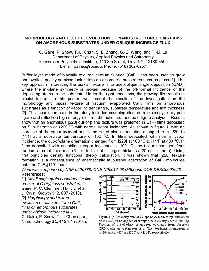
MORPHOLOGY AND TEXTURE EVOLUTION OF NANOSTRUCTURED CaF2 FILMS ON AMORPHOUS SUBSTRATES UNDER OBLIQUE INCIDENCE FLUX
C. Gaire, P. Snow, T.-L. Chan, S. B. Zhang, G.-C. Wang, and T.-M. Lu
Department of Physics, Applied Physics and Astronomy Rensselaer Polytechnic Institute, 110 8th Street, Troy, NY, 12180-3590
E-mail: [email protected], Phone: (518) 362-6257 Buffer layer made of biaxially textured calcium fluoride (CaF2) has been used to grow photovoltaic-quality semiconductor films on disordered substrates such as glass [1]. The key approach in creating the biaxial texture is to use oblique angle deposition (OAD), where the in-plane symmetry is broken because of the off-normal incidence of the depositing atoms to the substrate. Under the right conditions, the growing film results in biaxial texture. In this poster, we present the results of the investigation on the morphology and biaxial texture of vacuum evaporated CaF2 films on amorphous substrates as a function of vapor incident angle, substrate temperature and film thickness [2]. The techniques used in the study included scanning electron microscopy, x-ray pole figure and reflection high energy electron diffraction surface pole figure analyses. Results show that an anomalous [220] out-of-plane texture was preferred in CaF2 films deposited on Si substrates at <200 oC with normal vapor incidence. As shown in figure 1, with an increase of the vapor incident angle, the out-of-plane orientation changed from [220] to [111] at a substrate temperature of 100 oC. In films deposited with normal vapor incidence, the out-of-plane orientation changed from [220] at 100 oC to [111] at 400 oC. In films deposited with an oblique vapor incidence at 100 oC, the texture changed from random at small thickness (5 nm) to biaxial at larger thickness (20 nm or more). Using first principles density functional theory calculation, it was shown that [220] texture formation is a consequence of energetically favourable adsorption of CaF2 molecules onto the CaF2(110) facet. Work was supported by NSF-0506738, ONR N00014-08-0453 and DOE DESC0002623. References: [1] Small angle grain boundary Ge films on biaxial CaF2/glass substrates, C. Gaire, P. C. Clemmer, H.-F. Li et al., J. Cryst. Growth 312, 607 (2010). [2] Morphology and texture evolution of nanostructured CaF2 films on amorphous substrates under oblique incidence flux, C. Gaire, P. Snow, T.-L. Chan et al., Nanotechnology 21, 445701 (2010).
ELECTROCHEMICAL SYNTHESIS AND CHARACTERIZATION OF HIGH-FILLING COPPER NANOWIRE ARRAYS INTO PAAM TEMPLATES
Nan Li, Brian Willis Department of Chemical, Materials and Biomolecular Engineering, University of
Connecticut, Storrs, CT [email protected]
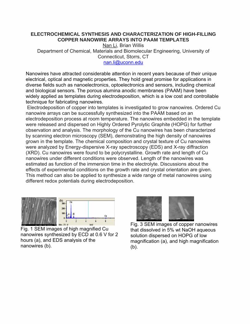
Nanowires have attracted considerable attention in recent years because of their unique electrical, optical and magnetic properties. They hold great promise for applications in diverse fields such as nanoelectronics, optoelectronics and sensors, including chemical and biological sensors. The porous alumina anodic membranes (PAAM) have been widely applied as templates during electrodeposition, which is a low cost and controllable technique for fabricating nanowires. Electrodeposition of copper into templates is investigated to grow nanowires. Ordered Cu nanowire arrays can be successfully synthesized into the PAAM based on an electrodeposition process at room temperature. The nanowires embedded in the template were released and dispersed on Highly Ordered Pyrolytic Graphite (HOPG) for further observation and analysis. The morphology of the Cu nanowires has been characterized by scanning electron microscopy (SEM), demonstrating the high density of nanowires grown in the template. The chemical composition and crystal texture of Cu nanowires were analyzed by Energy-dispersive X-ray spectroscopy (EDS) and X-ray diffraction (XRD). Cu nanowires were found to be polycrystalline. Growth rate and length of Cu nanowires under different conditions were observed. Length of the nanowires was estimated as function of the immersion time in the electrolyte. Discussions about the effects of experimental conditions on the growth rate and crystal orientation are given. This method can also be applied to synthesize a wide range of metal nanowires using different redox potentials during electrodeposition.
Fig. 3 SEM images of copper nanowires that dissolved in 5% wt NaOH aqueous solution dispersed on HOPG of low magnification (a), and high magnification (b).
Fig. 1 SEM images of high magnified Cu nanowires synthesized by ECD at 0.6 V for 2 hours (a), and EDS analysis of the nanowires (b).
OPTICAL PROPERTIES OF POLYCRYSTALLINE CHEMICAL VAPOR DEPOSITED (CVD) GRAPHENE GROWN ON COPPER FOILS INVESTIGATED WITH
SPECTROSCOPIC ELLIPSOMETRY (SE)
F. Nelson, 1 V. Kamineni,1 T. Zhang, 1 E. Comfort, 1 J. Lee, 1 A. C. Diebold1
1College of Nanoscale Science and Engineering
Contact email: [email protected]
The high carrier mobility of graphene makes it a potential material for future transistors and switching devices that may replace transistors. Yet much of the research has utilized the exfoliation, or "scotch-tape" technique of sample preparation. More scalable growth methods have been investigated, such as the thermal decomposition of SiC, and the resulting graphene films have properties dependent on their fabrication parameters. One potentially scalable technique is that of hydrocarbon gas-based CVD onto metallic substrates. Here, we report on the ellipsometric characterization of Single-Layer-Graphene (SLG) grown on copper foils and subsequently transferred to glass substrates). One of the expected challenges with development of a dispersion model for SLG is that the CVD graphene has many "grains" inside the measured area while previous reports of exfoliated graphene were done on single crystal samples. We find that CVD graphene has optical properties similar to exfoliated graphene. The absorption follows the expected ( is the fine structure constant) value over a large wavelength range. CVD Graphene also exhibits a “Van Hove singularity” at ~4.5 eV in the polarizability due to excitonic effects which red-shift the absorption peak found in the single-particle picture.
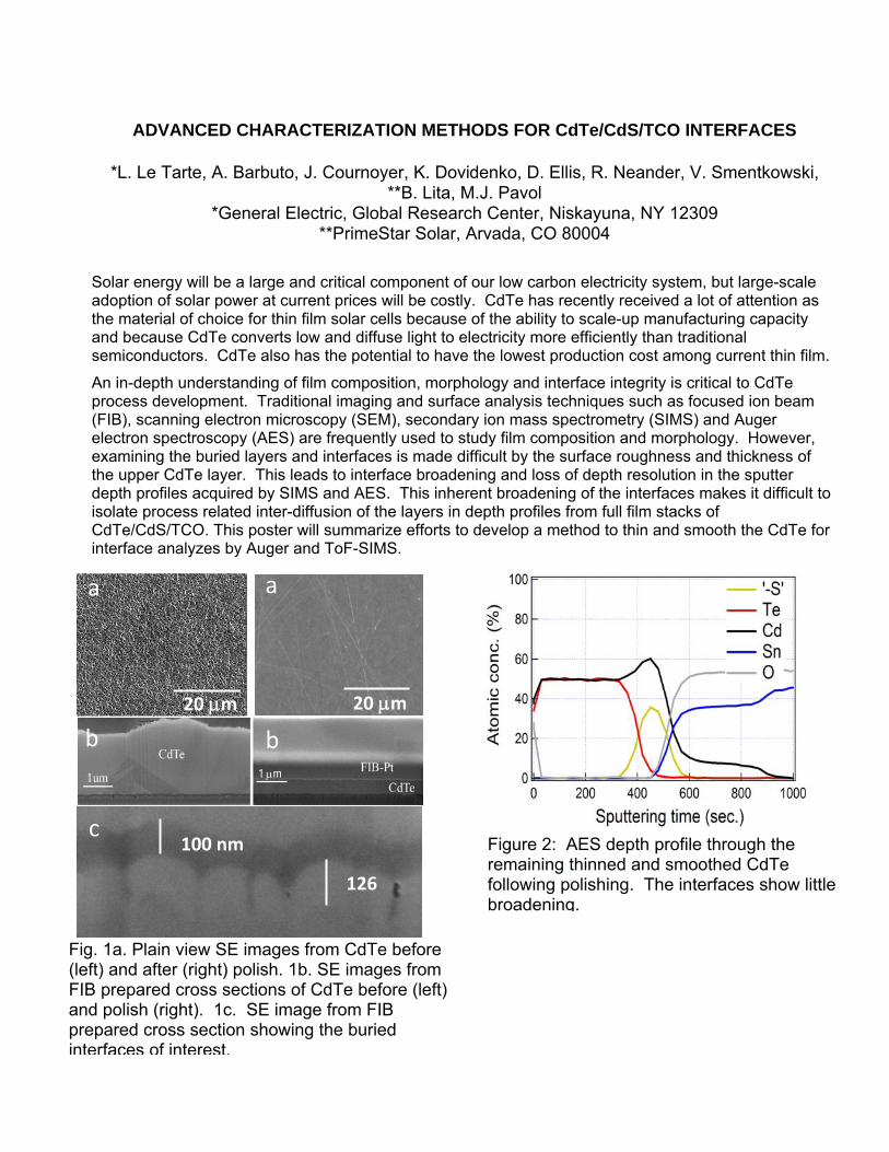
ADVANCED CHARACTERIZATION METHODS FOR CdTe/CdS/TCO INTERFACES
*L. Le Tarte, A. Barbuto, J. Cournoyer, K. Dovidenko, D. Ellis, R. Neander, V. Smentkowski, **B. Lita, M.J. Pavol
*General Electric, Global Research Center, Niskayuna, NY 12309 **PrimeStar Solar, Arvada, CO 80004
Solar energy will be a large and critical component of our low carbon electricity system, but large-scale adoption of solar power at current prices will be costly. CdTe has recently received a lot of attention as the material of choice for thin film solar cells because of the ability to scale-up manufacturing capacity and because CdTe converts low and diffuse light to electricity more efficiently than traditional semiconductors. CdTe also has the potential to have the lowest production cost among current thin film.
An in-depth understanding of film composition, morphology and interface integrity is critical to CdTe process development. Traditional imaging and surface analysis techniques such as focused ion beam (FIB), scanning electron microscopy (SEM), secondary ion mass spectrometry (SIMS) and Auger electron spectroscopy (AES) are frequently used to study film composition and morphology. However, examining the buried layers and interfaces is made difficult by the surface roughness and thickness of the upper CdTe layer. This leads to interface broadening and loss of depth resolution in the sputter depth profiles acquired by SIMS and AES. This inherent broadening of the interfaces makes it difficult to isolate process related inter-diffusion of the layers in depth profiles from full film stacks of CdTe/CdS/TCO. This poster will summarize efforts to develop a method to thin and smooth the CdTe for interface analyzes by Auger and ToF-SIMS.
Figure 2: AES depth profile through the remaining thinned and smoothed CdTe following polishing. The interfaces show little broadening.
20m 20m
100 nm
126
a a
b b
c
Fig. 1a. Plain view SE images from CdTe before (left) and after (right) polish. 1b. SE images from FIB prepared cross sections of CdTe before (left) and polish (right). 1c. SE image from FIB prepared cross section showing the buried interfaces of interest.
1 m
NEW POSSIBILITIES IN HIGH SENSITIVITY LOW ENERGY ION SCATTERING (LEIS) FOR PROBING THE OUTERMOST ATOMIC LAYER
A. Schnieders1,2, Thomas Grehl3, Philipp Brüner3, Hidde Brongersma3,4, Michael Fartmann4, Rik ter Veen4 N. Havercroft2
1 Tascon USA, Inc., 100 Red Schoolhouse Road, Chestnut Ridge, NY 10977, USA 2 ION-TOF USA, Inc., 100 Red Schoolhouse Road, Chestnut Ridge, NY 10977, USA
3 ION-TOF GmbH, Heisenbergstr. 15, 48149 Muenster, Germany 4 Tascon GmbH, Heisenbergstr. 15, 48149 Muenster, Germany
e-mail: [email protected]
Low Energy Ion Scattering (LEIS) is an extremely surface sensitive analytical technique for the characterization and quantification of the composition of the outermost atomic layer. This information is required to understand material properties like catalytic performance or the nucleation and initial growth modes of ultra-thin films, e. g. in nanoelectronics.
The Qtac100 is a high sensitivity and high resolution LEIS instrument with innovative capabilities making a wide range of new applications available.
LEIS gains from the choice of different noble gas ions available on the Qtac100. Helium is used for non-destructive depth profiling and light element surface characterization. For the analysis of higher-mass elements, heavier primary ions can be chosen, which provides superior mass resolution. The higher energy range of the primary ion source of up to 8 keV, also improves the mass resolution. For example, it is now possible to separate Au and Pt or Ag and Pd, which are both relevant to the field of catalysis.
In addition, a time-of-flight (ToF) filter dramatically improves the detection limits by suppressing the signal arising from sputtered ions while allowing the scattered ions to reach the detection system. Our results show that quantification is feasible for real-world samples with coverages of a few 10 ppm of one monolayer, utilising the high primary ion energy and ToF filtering of the Qtac100.
Further possibilities such as localized analysis and depth profiling (both traditional sputter profiling, as well as non-destructive (static) profiling) will be also discussed.
METROLOGY AND MANIPULATION OF HEAT TRANSPORT AT METAL-DIELECTRIC
INTERFACES
Peter O’Brien1, Jianxun Liu2, Ranganath Teki1, Masashi Yamaguchi2, Pawel Keblinski1, Ganpati Ramanath1
1 Department of Materials Science and Engineering, and
2 Department of Physics, Rensselaer Polytechnic Institute, Troy, NY.
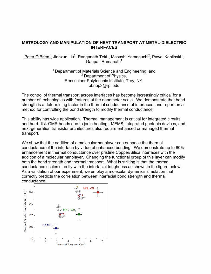
The control of thermal transport across interfaces has become increasingly critical for a number of technologies with features at the nanometer scale. We demonstrate that bond strength is a determining factor in the thermal conductance of interfaces, and report on a method for controlling the bond strength to modify thermal conductance. This ability has wide application. Thermal management is critical for integrated circuits and hard-disk GMR heads due to joule heating. MEMS, integrated photonic devices, and next-generation transistor architectures also require enhanced or managed thermal transport. We show that the addition of a molecular nanolayer can enhance the thermal conductance of the interface by virtue of enhanced bonding. We demonstrate up to 60% enhancement in thermal conductance over pristine Copper/Silica interfaces with the addition of a molecular nanolayer. Changing the functional group of this layer can modify both the bond strength and thermal transport. What is striking is that the thermal conductance scales directly with the interfacial toughness as shown in the figure below. As a validation of our experiment, we employ a molecular dynamics simulation that correctly predicts the correlation between interfacial bond strength and thermal conductance.

NANOSCALE ELECTRON EMITTER LIFETIME: THE ROLE OF HEAT CONDUCTION
J. Scott Price
GE Global Research 1 Research Circle
Niskayuna, NY 12309
Nano-scale devices replace electron emitters that use temperature and electric field to promote emission. Field emission from very thin, robust, emitter structures benefits from the small diameter of tip; modest applied voltage differences produce high electric fields. Some emitter aspects remain the same, however, heat generated due to the passage of electrical current can affect structures to render them better or poorer current dispensing devices. Some calculations will be presented along with comparison to experimental evidence to evaluate the models used to characterize the structures.
VISUALIZE THE EXTRUSION AND VOIDS INDUCED IN COPPER-FILLED THROUGH-SILICON VIAS (TSVS) AT VARIOUS TEMPERATURES USING X-RAY MICROSCOPY
LayWai Kong1, Andrew C. Rudack2, Peter Krueger3, Ehrenfried Zschech3,
Sitaram Arkalgud2, A.C. Diebold1
College of Nanoscale Science and Engineering, University at Albany, Albany, N.Y. 122031
SEMATECH, Albany, N.Y. 122032 Fraunhofer Institute for Nondestructive Testing (IZFP), Dresden, Germany3
255 Fuller Road 12203 Albany, NY 1 [email protected]; (518) 437-8686
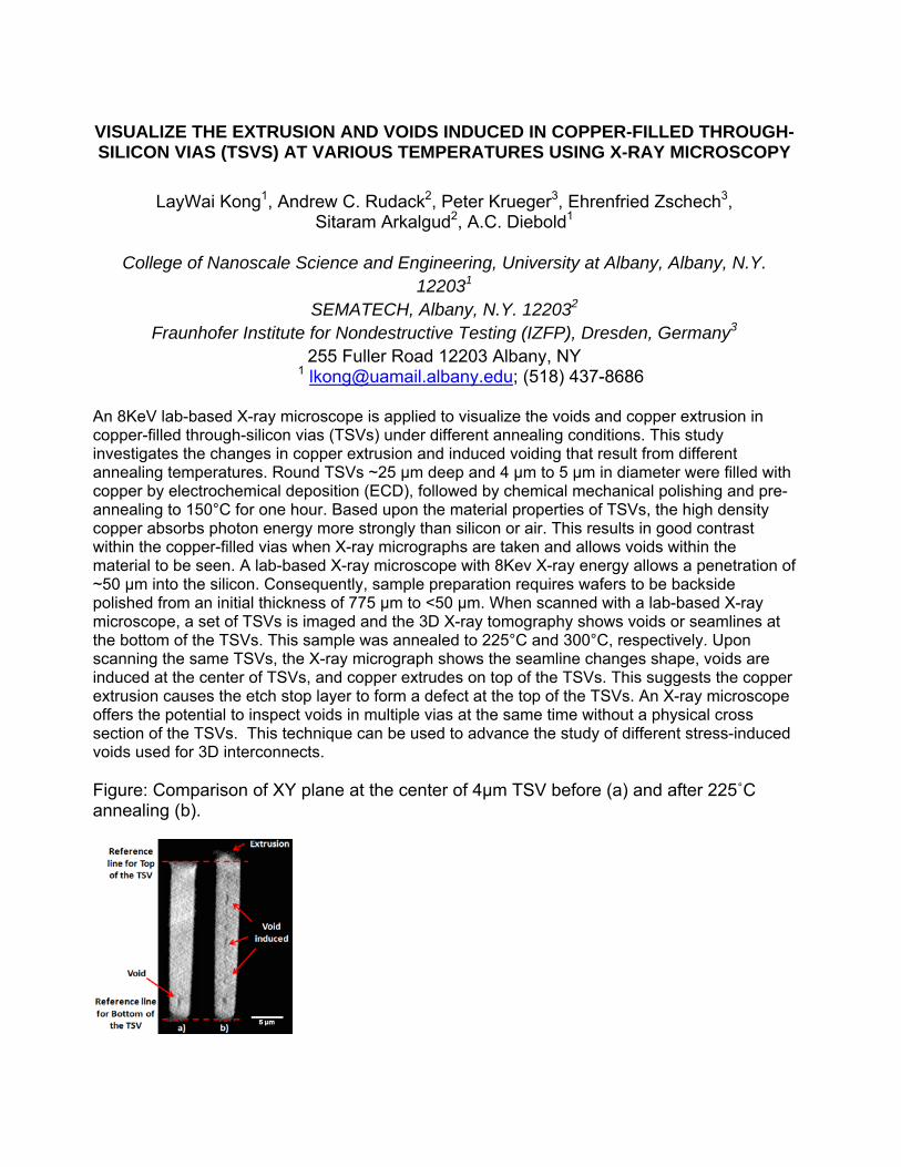
An 8KeV lab-based X-ray microscope is applied to visualize the voids and copper extrusion in copper-filled through-silicon vias (TSVs) under different annealing conditions. This study investigates the changes in copper extrusion and induced voiding that result from different annealing temperatures. Round TSVs ~25 µm deep and 4 µm to 5 µm in diameter were filled with copper by electrochemical deposition (ECD), followed by chemical mechanical polishing and pre-annealing to 150°C for one hour. Based upon the material properties of TSVs, the high density copper absorbs photon energy more strongly than silicon or air. This results in good contrast within the copper-filled vias when X-ray micrographs are taken and allows voids within the material to be seen. A lab-based X-ray microscope with 8Kev X-ray energy allows a penetration of ~50 µm into the silicon. Consequently, sample preparation requires wafers to be backside polished from an initial thickness of 775 µm to <50 µm. When scanned with a lab-based X-ray microscope, a set of TSVs is imaged and the 3D X-ray tomography shows voids or seamlines at the bottom of the TSVs. This sample was annealed to 225°C and 300°C, respectively. Upon scanning the same TSVs, the X-ray micrograph shows the seamline changes shape, voids are induced at the center of TSVs, and copper extrudes on top of the TSVs. This suggests the copper extrusion causes the etch stop layer to form a defect at the top of the TSVs. An X-ray microscope offers the potential to inspect voids in multiple vias at the same time without a physical cross section of the TSVs. This technique can be used to advance the study of different stress-induced voids used for 3D interconnects. Figure: Comparison of XY plane at the center of 4μm TSV before (a) and after 225˚C annealing (b).
MODELING THE IMPACT OF COPPER PLASTICITY ON THERMO-MECHANICAL STRESS INDUCED BY THROUGH-SILICON VIAS (TSVS)
Ben Backes1, Colin McDonough1, Jihan Capulong1, Larry Smith2, Tom Jing1, Robert
Geer1, and Wei Wang1
1 College of Nanoscale Science and Engineering, University at Albany, Albany, NY, 12203
2 SEMATECH, Albany, NY 12203
Email: [email protected], Phone: 708-415-2920 The development of 3D interconnection methods for future generations of integrated circuits is imperative for meeting further device scaling demands, as interconnect delay is fast becoming a performance-limiting factor. In addition, 3D die stacking can significantly improve the areal efficiency and functionality of future chips. The use of copper through-silicon vias (TSVs) is a highly promising avenue for 3D integration, but their propensity for modifying the stress profile in the surrounding silicon leads to concerns about the impact on the performance of nearby devices. While the copper in TSVs can have a complex grain structure and incorporate impurities, an assumption of aggregate elasto-plastic behavior has been shown to approximate measured stress profiles [1]. In this study, we further investigate the impact of copper’s plastic properties on the residual stress profile close to minimally processed TSVs, both isolated and in linear arrays. The results of simulations using a linear isotropic hardening model show that some measure of control over the deposited copper films is desirable, as variability in the films can dramatically change the magnitude of stress near the TSV.
Reference: [1] C. Okoro, et al., "Extraction of the Appropriate Material Property for Realistic Modeling of Through-Silicon-Vias using μ-Raman Spectroscopy," in Proc. IITC, pp. 16-18 (2008).
NANOSCALE FABRICATION AND CHARACTERIZATION FOR MATERIALS FOR BEYOND-CMOS DEVICES
Prabhu Balasubramanian1, Delia Bearup1*, Adam Bross1, See Wee Chee1, Jeremey
Graham2, Li He1, Jessica Murphy1*, Hamed Parvaneh1, Xiaowei Wu1 and Robert Hull1 1. Dept. of Materials Science and Engineering, Rensselaer Polytechnic Institute (*Now
graduated) 2. Dept. of Engineering Physics, University of Virginia
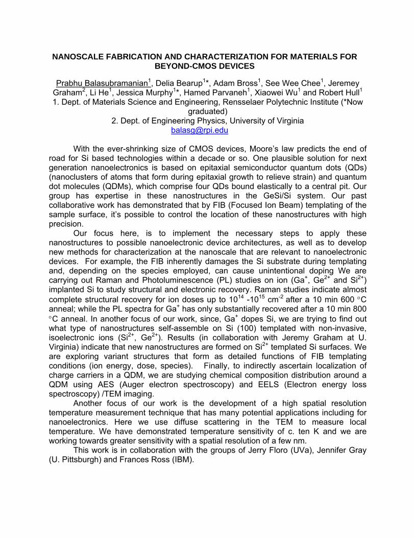
With the ever-shrinking size of CMOS devices, Moore’s law predicts the end of road for Si based technologies within a decade or so. One plausible solution for next generation nanoelectronics is based on epitaxial semiconductor quantum dots (QDs) (nanoclusters of atoms that form during epitaxial growth to relieve strain) and quantum dot molecules (QDMs), which comprise four QDs bound elastically to a central pit. Our group has expertise in these nanostructures in the GeSi/Si system. Our past collaborative work has demonstrated that by FIB (Focused Ion Beam) templating of the sample surface, it’s possible to control the location of these nanostructures with high precision. Our focus here, is to implement the necessary steps to apply these nanostructures to possible nanoelectronic device architectures, as well as to develop new methods for characterization at the nanoscale that are relevant to nanoelectronic devices. For example, the FIB inherently damages the Si substrate during templating and, depending on the species employed, can cause unintentional doping We are carrying out Raman and Photoluminescence (PL) studies on ion (Ga+, Ge2+ and Si2+) implanted Si to study structural and electronic recovery. Raman studies indicate almost complete structural recovery for ion doses up to 1014 -1015 cm-2 after a 10 min 600 C anneal; while the PL spectra for Ga+ has only substantially recovered after a 10 min 800 C anneal. In another focus of our work, since, Ga+ dopes Si, we are trying to find out what type of nanostructures self-assemble on Si (100) templated with non-invasive, isoelectronic ions (Si2+, Ge2+). Results (in collaboration with Jeremy Graham at U. Virginia) indicate that new nanostructures are formed on Si2+ templated Si surfaces. We are exploring variant structures that form as detailed functions of FIB templating conditions (ion energy, dose, species). Finally, to indirectly ascertain localization of charge carriers in a QDM, we are studying chemical composition distribution around a QDM using AES (Auger electron spectroscopy) and EELS (Electron energy loss spectroscopy) /TEM imaging. Another focus of our work is the development of a high spatial resolution temperature measurement technique that has many potential applications including for nanoelectronics. Here we use diffuse scattering in the TEM to measure local temperature. We have demonstrated temperature sensitivity of c. ten K and we are working towards greater sensitivity with a spatial resolution of a few nm. This work is in collaboration with the groups of Jerry Floro (UVa), Jennifer Gray (U. Pittsburgh) and Frances Ross (IBM).
MAKING MOLECULAR MULTILAYERS USING “CLICK” CHEMISTRY: GROWTH AND THIN FILM CHARACTERIZATION
Peter K. B. Palomaki and Peter H. Dinolfo
Department of Chemistry & Chemical Biology and The Baruch ‘60 Center for Biochemical
Solar Energy Research Rensselaer Polytechnic Institute, 110 8th Street, Troy, NY 12180
Email: [email protected]
Bottom-up approaches to creating molecular multilayer assemblies using layer-by-layer (LbL) techniques give one the ability to tailor the surface properties of an interface. LbL assembly methods can provide molecular level control of structure in one dimension from simple solution deposition processes. We have developed a versatile LbL fabrication method using copper(I)-catalyzed azide-alkyne cycloaddition (CuAAC) or “click” chemistry in the construction of multilayer assemblies on oxide surfaces.1 These reactions occur in minutes at room temperature allowing for the facile creation of complex, covalently attached multilayer assemblies. Multilayers containing synthetic porphyrins, perylenes, and mixtures of the two have been constructed in order to highlight the versatility of this method. The fabrication of this new type of molecular multilayer thin film will be discussed along with characterization of the photophysical, electrochemical, and structural properties. The benefits of this type of multilayer growth are simple and rapid solution deposition of covalently bound multilayer assemblies with specifically designed electrochemical and optical properties.
2. Palomaki, P.K.B. and Dinolfo, P.H “A Versatile Molecular Layer-by-Layer Thin Film Fabrication Technique Utilizing Copper(I)-Catalyzed Azide-Alkyne Cycloaddition” Langmuir 2010, 26 (12), 9677-9685.

Electronic Poster
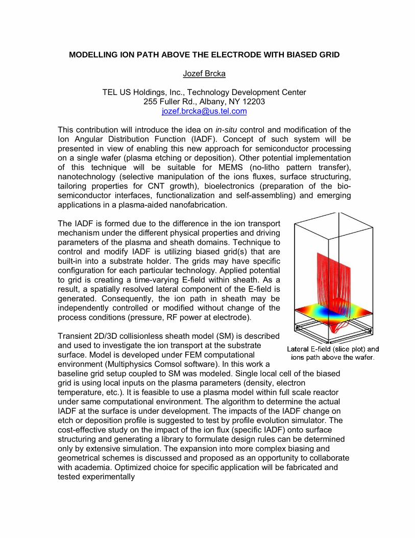
MODELLING ION PATH ABOVE THE ELECTRODE WITH BIASED GRID
Jozef Brcka
TEL US Holdings, Inc., Technology Development Center 255 Fuller Rd., Albany, NY 12203
[email protected] This contribution will introduce the idea on in-situ control and modification of the Ion Angular Distribution Function (IADF). Concept of such system will be presented in view of enabling this new approach for semiconductor processing on a single wafer (plasma etching or deposition). Other potential implementation of this technique will be suitable for MEMS (no-litho pattern transfer), nanotechnology (selective manipulation of the ions fluxes, surface structuring, tailoring properties for CNT growth), bioelectronics (preparation of the bio-semiconductor interfaces, functionalization and self-assembling) and emerging applications in a plasma-aided nanofabrication. The IADF is formed due to the difference in the ion transport mechanism under the different physical properties and driving parameters of the plasma and sheath domains. Technique to control and modify IADF is utilizing biased grid(s) that are built-in into a substrate holder. The grids may have specific configuration for each particular technology. Applied potential to grid is creating a time-varying E-field within sheath. As a result, a spatially resolved lateral component of the E-field is generated. Consequently, the ion path in sheath may be independently controlled or modified without change of the process conditions (pressure, RF power at electrode). Transient 2D/3D collisionless sheath model (SM) is described and used to investigate the ion transport at the substrate surface. Model is developed under FEM computational environment (Multiphysics Comsol software). In this work a baseline grid setup coupled to SM was modeled. Single local cell of the biased grid is using local inputs on the plasma parameters (density, electron temperature, etc.). It is feasible to use a plasma model within full scale reactor under same computational environment. The algorithm to determine the actual IADF at the surface is under development. The impacts of the IADF change on etch or deposition profile is suggested to test by profile evolution simulator. The cost-effective study on the impact of the ion flux (specific IADF) onto surface structuring and generating a library to formulate design rules can be determined only by extensive simulation. The expansion into more complex biasing and geometrical schemes is discussed and proposed as an opportunity to collaborate with academia. Optimized choice for specific application will be fabricated and tested experimentally