Embed Size (px)
Citation preview
i
Enterprise Server GroupIntel N440BX Server
Technical Product Specification
Version 2.0Order Number: 243701-002
April, 1999
The Intel N440BX Server may contain design defects or errors known as errata. Characterized errata that may cause the
N440BX Server’s behavior to deviate from published specifications are documented in the N440BX Server Specification Update.
ii
Revision History
Revision Revision History Date
Rev 1.0 Initial release of the Intel N440BX Server Technical Product Specification 2/98
Rev 2.0 Updated and included specification updates changes. 4/99
NOTE: If printing this document from an electronic file, use a PostScript printer with the appropriatePostScript print driver to insure the drawings print clearly.
Information in this document is provided in connection with Intel products. No license, express or implied, by estoppel or
otherwise, to any intellectual property rights is granted by this document. Except as provided in Intel’s Terms and
Conditions of Sale for such products, Intel assumes no liability whatsoever, and Intel disclaims any express or implied
warranty, relating to sale and/or use of Intel products including liability or warranties relating to fitness for a particular
purpose, merchantability, or infringement of any patent, copyright or other intellectual property right. Intel products are not
intended for use in medical, life saving, or life sustaining applications. Intel may make changes to specifications and
product descriptions at any time, without notice.
The Intel products referred to in this document may contain design defects or errors known as errata which may cause
the product to deviate from published specifications. Current characterized errata are available on request.
Contact your local Intel sales office or your distributor to obtain the latest specifications and before placing your product
order.
Copyright © Intel Corporation 1998. *Third-party brands and names are the property of their respective owners.
iv
Table of Contents
1. Board Set Descriptions........................................................................................................................ 7
1.1. Product Overview .........................................................................................................................................7
1.2. Baseboard Diagram .....................................................................................................................................9
1.3 Back Panel Connectors ..............................................................................................................................10
1.4 Jumpers......................................................................................................................................................11
1.5. Baseboard Architecture Overview ..............................................................................................................14
1.6. Pentium® II/ Pentium® III Processor(s) .....................................................................................................15
1.7. VRM ...........................................................................................................................................................15
1.8. 440BX Host Bridge / Memory Controller ....................................................................................................15
1.9. PCI SCSI Subsystem .................................................................................................................................16
1.10. PCI Network Interface Subsystem..............................................................................................................16
1.11. PCI Video Subsystem.................................................................................................................................16
1.12. ISA I/O Subsystem .....................................................................................................................................17
1.13. National 87309 SuperI/O Controller ...........................................................................................................17
1.14. I/O APIC .....................................................................................................................................................17
1.15. Flash BIOS .................................................................................................................................................17
1.16. Server Management Subsystem ................................................................................................................17
1.17. Basic Utility Device .....................................................................................................................................18
1.18. Universal Retention Module .......................................................................................................................18
1.19. Processor Bus Termination/Regulation/Power...........................................................................................19
1.20. Termination Card........................................................................................................................................19
1.21. Functional Architecture...............................................................................................................................19
1.22. Processor/PCI Host Bridge/Memory Subsystem ........................................................................................21
1.23. APIC Bus....................................................................................................................................................22
1.24. Miscellaneous Processor/Memory Subsystem Circuitry .............................................................................23
1.25. Processor Core Frequency and Memory Configuration Logic....................................................................23
1.26 Processor Card Presence Detection ..........................................................................................................23
1.27. PCI I/O Subsystem.....................................................................................................................................23
1.28. PCI Arbitration ............................................................................................................................................24
1.29. PIIX4...........................................................................................................................................................25
1.30. SCSI Subsystem ........................................................................................................................................28
1.31. PCI Video ...................................................................................................................................................31
1.32. Video Chip PCI Signals ..............................................................................................................................31
1.33. Network Interface Controller (NIC) .............................................................................................................35
1.34. ISA I/O Subsystem .....................................................................................................................................36
1.35. Compatibility I/O Controller Subsystem......................................................................................................37
1.37. System Reset Control.................................................................................................................................38
1.38. Clock Generation and Distribution..............................................................................................................40
v
1.39. Interrupts and I/O APIC ..............................................................................................................................41
1.40. Interrupt Sources........................................................................................................................................43
1.41. Boot Order..................................................................................................................................................45
1.42. System Management Interrupt Handling ....................................................................................................45
1.43. Basic Utility Device (BUD) ..........................................................................................................................45
2. Server Management ........................................................................................................................... 50
2.1. Overview ....................................................................................................................................................50
2.2. Server Management Bus............................................................................................................................51
2.3. Intelligent Management Bus.......................................................................................................................51
2.4. Chassis Intrusion........................................................................................................................................53
2.5. Baseboard Management Controller (BMC) ................................................................................................54
2.6. Emergency Management Port (EMP).........................................................................................................56
2.7. Fault Resilient Booting ...............................................................................................................................57
2.8. System Fan Interface .................................................................................................................................57
3. Memory and Other Resource Mappings .......................................................................................... 59
3.1. Memory Space ...........................................................................................................................................59
3.2. DOS Compatibility Region..........................................................................................................................60
3.3. DOS Area ...................................................................................................................................................61
3.4. ISA Window Memory..................................................................................................................................61
3.5. Video or SMM Memory...............................................................................................................................61
3.6. Add-in Card BIOS and Buffer Area.............................................................................................................61
3.7. Extended System BIOS..............................................................................................................................61
3.8. System BIOS..............................................................................................................................................61
3.9. Extended Memory ......................................................................................................................................61
3.10. Main Memory..............................................................................................................................................62
3.11. PCI Memory Space ....................................................................................................................................62
3.12. High BIOS ..................................................................................................................................................63
3.13. I/O APIC Configuration Space....................................................................................................................63
3.14. Extended Pentium II/Pentium III Processor Region (above 4GB) ..............................................................63
3.15. Memory Shadowing....................................................................................................................................63
3.16. SMM Mode Handling..................................................................................................................................63
3.17. I/O Map.......................................................................................................................................................64
3.18. Accessing Configuration Space..................................................................................................................66
3.19. Error Handling ............................................................................................................................................68
3.20. Hardware Initialization and Configuration...................................................................................................68
3.21. System Initialization Sequence...................................................................................................................68
3.22. Server Management Programming Interface .............................................................................................69
3.23. PCI Interrupt to IRQ Routing Control..........................................................................................................69
4. BIOS..................................................................................................................................................... 71

vi
4.1. BIOS...........................................................................................................................................................71
4.2. System BIOS..............................................................................................................................................74
4.3. Security Features .......................................................................................................................................74
4.4. Auto-Configuration Features ......................................................................................................................77
4.5. Performance Features................................................................................................................................81
4.6. Reliability Features.....................................................................................................................................83
4.7. Console Redirection ...................................................................................................................................88
4.8. BIOS Revision History Format....................................................................................................................90
5. Configuration Utility........................................................................................................................... 91
5.1 Configuration Utilities Overview..................................................................................................................91
5.2 Configurable Options..................................................................................................................................91
5.3. Setup Utility Operation ...............................................................................................................................95
6. Flash Update Utility .......................................................................................................................... 107
6.1 Loading the System BIOS ........................................................................................................................107
6.2 User Binary Area ......................................................................................................................................108
6.3 Diagnostic Boot Loader Partition..............................................................................................................108
6.4 Language Area.........................................................................................................................................108
6.5 Recovery Mode ........................................................................................................................................108
7. Error Handling .................................................................................................................................. 109
7.1 Error Sources and Types..........................................................................................................................109
7.2 Error Handlers ..........................................................................................................................................109
7.3 Handling and logging System Errors ........................................................................................................110
7.4 Error Messages and Error Codes.............................................................................................................114
8. Board Set Specifications ................................................................................................................. 122
8.1. Absolute Maximum Ratings......................................................................................................................122
8.2. Electrical Specifications............................................................................................................................122
8.3. Power Connection ....................................................................................................................................123
8.4. Power Consumption .................................................................................................................................124
8.5. Power Supply Specifications ....................................................................................................................125
9. Errata Listing .................................................................................................................................... 128
9.1. Summary Errata Table .............................................................................................................................128
9.2. ERRATA...................................................................................................................................................129
7
1. Board Set Descriptions
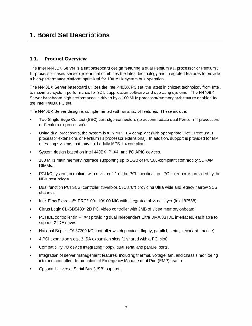
1.1. Product Overview
The Intel N440BX Server is a flat baseboard design featuring a dual Pentium® II processor or Pentium®III processor based server system that combines the latest technology and integrated features to providea high-performance platform optimized for 100 MHz system bus operation.
The N440BX Server baseboard utilizes the Intel 440BX PCIset, the latest in chipset technology from Intel,to maximize system performance for 32-bit application software and operating systems. The N440BXServer baseboard high performance is driven by a 100 MHz processor/memory architecture enabled bythe Intel 440BX PCIset.
The N440BX Server design is complemented with an array of features. These include:
• Two Single Edge Contact (SEC) cartridge connectors (to accommodate dual Pentium II processorsor Pentium III processor).
• Using dual processors, the system is fully MPS 1.4 compliant (with appropriate Slot 1 Pentium IIprocessor extensions or Pentium III processor extensions). In addition, support is provided for MPoperating systems that may not be fully MPS 1.4 compliant.
• System design based on Intel 440BX, PIIX4, and I/O APIC devices.
• 100 MHz main memory interface supporting up to 1GB of PC/100-compliant commodity SDRAMDIMMs.
• PCI I/O system, compliant with revision 2.1 of the PCI specification. PCI interface is provided by theNBX host bridge
• Dual function PCI SCSI controller (Symbios 53C876*) providing Ultra wide and legacy narrow SCSIchannels.
• Intel EtherExpress™ PRO/100+ 10/100 NIC with integrated physical layer (Intel 82558)
• Cirrus Logic CL-GD5480* 2D PCI video controller with 2MB of video memory onboard.
• PCI IDE controller (in PIIX4) providing dual independent Ultra DMA/33 IDE interfaces, each able tosupport 2 IDE drives.
• National Super I/O* 87309 I/O controller which provides floppy, parallel, serial, keyboard, mouse).
• 4 PCI expansion slots, 2 ISA expansion slots (1 shared with a PCI slot).
• Compatibility I/O device integrating floppy, dual serial and parallel ports.
• Integration of server management features, including thermal, voltage, fan, and chassis monitoringinto one controller. Introduction of Emergency Management Port (EMP) feature.
• Optional Universal Serial Bus (USB) support.
8
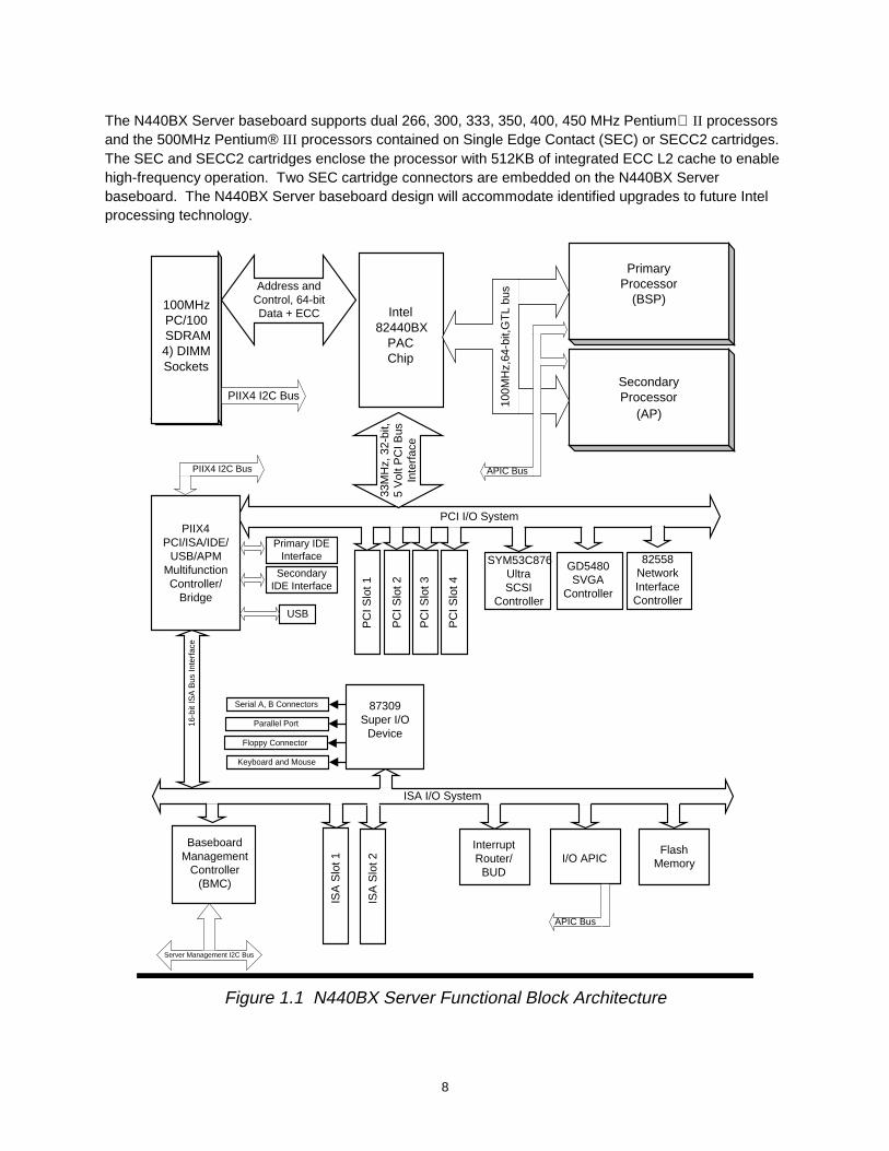
The N440BX Server baseboard supports dual 266, 300, 333, 350, 400, 450 MHz Pentium II processorsand the 500MHz Pentium® III processors contained on Single Edge Contact (SEC) or SECC2 cartridges.The SEC and SECC2 cartridges enclose the processor with 512KB of integrated ECC L2 cache to enablehigh-frequency operation. Two SEC cartridge connectors are embedded on the N440BX Serverbaseboard. The N440BX Server baseboard design will accommodate identified upgrades to future Intelprocessing technology.
100M
Hz,
64-b
it,G
TL
bus
16-b
it IS
A B
us In
terf
ace
PCI I/O System
87309Super I/O
Device
Serial A, B Connectors
Parallel Port
Floppy Connector
Keyboard and Mouse
ISA I/O System
PrimaryProcessor
(BSP)Intel
82440BXPACChip
33M
Hz,
32-
bit,
5 V
olt P
CI B
usIn
terf
ace
SecondaryProcessor
(AP)
BaseboardManagement
Controller(BMC)
I/O APICFlash
Memory
ISA
Slo
t 1
ISA
Slo
t 2P
CI S
lot 1
PC
I Slo
t 2
PC
I Slo
t 3
PC
I Slo
t 4
Server Management I2C Bus
InterruptRouter/
BUD
USB
PIIX4PCI/ISA/IDE/
USB/APMMultifunctionController/
Bridge
Primary IDEInterface
SecondaryIDE Interface
100MHzPC/100 SDRAM4) DIMMSockets
Address andControl, 64-bitData + ECC
PIIX4 I2C Bus
PIIX4 I2C Bus APIC Bus
APIC Bus
82558NetworkInterfaceController
GD5480SVGA
Controller
SYM53C876UltraSCSI
Controller
Figure 1.1 N440BX Server Functional Block Architecture
9
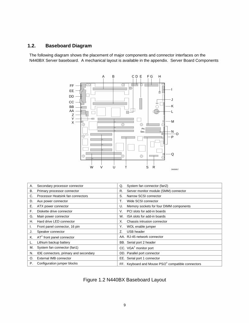
1.2. Baseboard Diagram
The following diagram shows the placement of major components and connector interfaces on theN440BX Server baseboard. A mechanical layout is available in the appendix. Server Board Components
Z
F G HA C D EB
I
L
J
NO
P
Q
K
MX
W UV T S R
Y
DD
BBCC
AA
Pri.Sec.
OM06957
EE
FF
A. Secondary processor connector Q. System fan connector (fan2)
B. Primary processor connector R. Server monitor module (SMM) connector
C. Processor Heatsink fan connectors S. Narrow SCSI connector
D. Aux power connector T. Wide SCSI connector
E. ATX power connector U. Memory sockets for four DIMM components
F. Diskette drive connector V. PCI slots for add-in boards
G. Main power connector W. ISA slots for add-in boards
H. Hard drive LED connector X. Chassis intrusion connector
I. Front panel connector, 16 pin Y. WOL enable jumper
J. Speaker connector Z. USB header
K. AT† front panel connector AA. RJ-45 network connector
L. Lithium backup battery BB. Serial port 2 header
M. System fan connector (fan1) CC. VGA† monitor port
N. IDE connectors, primary and secondary DD. Parallel port connector
O. External IMB connector EE. Serial port 1 connector
P. Configuration jumper blocks FF. Keyboard and Mouse PS/2† compatible connectors
Figure 1.2 N440BX Baseboard Layout
10
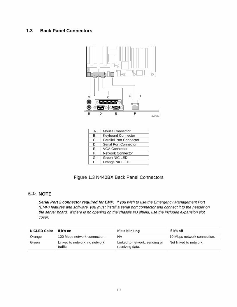
1.3 Back Panel Connectors
OM07054B D F
A
E
C G H
A. Mouse ConnectorB. Keyboard ConnectorC. Parallel Port ConnectorD. Serial Port ConnectorE. VGA ConnectorF. Network ConnectorG. Green NIC LEDH. Orange NIC LED
Figure 1.3 N440BX Back Panel Connectors
NOTE
Serial Port 2 connector required for EMP: If you wish to use the Emergency Management Port(EMP) features and software, you must install a serial port connector and connect it to the header onthe server board. If there is no opening on the chassis I/O shield, use the included expansion slotcover.
NICLED Color If it’s on If it’s blinking If it’s off
Orange 100 Mbps network connection. NA 10 Mbps network connection.
Green Linked to network, no networktraffic.
Linked to network, sending orreceiving data.
Not linked to network.

11
1.4 Jumpers
One 12-pin single inline header and one 9-pin single inline header provide seven 3-pin jumper blocks thatcontrol various configuration options, as shown in the figure below. The shaded areas show defaultjumper placement for each configurable option. Refer to the N440BX Product Guide for moreinformation.
OM08097
9
5
1
13
C
B
A
F
G
E
D
9
5
1
11
J3J2
IJ5B1
31
31
HJ3J1
Figure 1.4 N440BX Jumper Connectors
Jumper Block Pins (default in bold) What it does at system reset
A. BMC Forced Update Mode 9-10, Normal System boots normally.
10-11, Program System tries to update BMC firmware.
B. Chassis Intrusion Detection 5-6, Enable Switch installed on chassis indicates when cover has been removed.
6-7, Disable Chassis intrusion switch is bypassed.
C. FRB Timer Enable 1-2, Enable FRB operation is enabled (system boots from processor 1 ifprocessor 0 fails).
2-3, Disable FRB is disabled.
D. Boot Block Write Protect 13-14, Protect BIOS boot block is write-protected.
14-15Erase/Program
BIOS boot block is erasable and programmable.
E. Recovery Boot 9-10, Normal System attempts to boot using the BIOS stored in flash memory.
10-11, Recovery BIOS attempts a recovery boot, loading BIOS code from a floppydiskette into the flash device. This is typically used when the BIOScode has been corrupted.
F. Password clear 5-6, Protect Maintains the current system password.
6-7, Erase Clears the password.
G. CMOS clear 1-2, Protect Preserves the contents of NVRAM.
2-3, Erase Replaces the contents of NVRAM with the manufacturing defaultsettings.
H. BMC boot block write protect 1-2, Protect BMC boot block is write protected.
2-3, Erase/Program BMC boot block is erasable and programmable.
I. WOL Enable 1-2, Disabled Disables Wake On LAN. If your power supply does not provide 0.8 Aof +5 V Standby current, you must move the WOL Enable jumper to

12
this position.
2-3, Enabled Enables Wake On LAN.
CAUTIONMoving either of the boot block write protect jumpers (J3J2-D or J3J1) may cause significantdamage to the server board. Only move these jumpers when directed to by your customer servicerepresentative.
NOTE
+5 V Standby required for WOL: If you wish to use the WOL feature, your power supply mustprovide 0.8 A of +5 V Standby current. If it does not, your server board may not boot. Move theWOL Enable jumper to the Disabled position if your power supply does not provide the requiredcurrent.
13
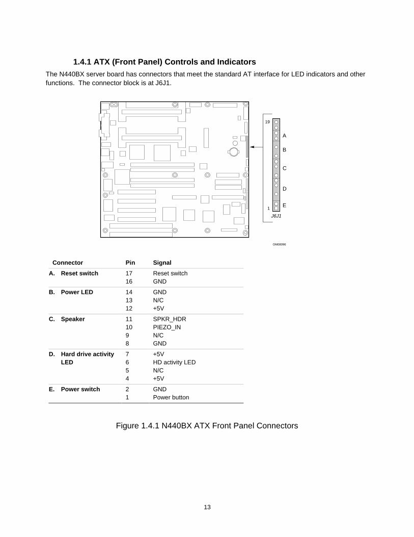
1.4.1 ATX (Front Panel) Controls and IndicatorsThe N440BX server board has connectors that meet the standard AT interface for LED indicators and otherfunctions. The connector block is at J6J1.
OM08096
A
B
C
D
E
19
1
J6J1
Connector Pin Signal
A. Reset switch 1716
Reset switchGND
B. Power LED 141312
GNDN/C+5V
C. Speaker 111098
SPKR_HDRPIEZO_INN/CGND
D. Hard drive activityLED
7654
+5VHD activity LEDN/C+5V
E. Power switch 21
GNDPower button
Figure 1.4.1 N440BX ATX Front Panel Connectors
14
1.5. Baseboard Architecture Overview
N440BX Server baseboard architecture is based on a design supporting dual processor operation usingPentium® II SEC or SECC2 cartridges, Pentium® III SECC2 cartridges and the Intel 440BX PCIset.N440BX provides a PCI-based I/O subsystem containing embedded devices for video, NIC, SCSI, andIDE, along with an ISA bridge to support compatibility devices. The baseboard also provides ServerManagement, and monitoring hardware support and interrupt control that supports dual processor andPC/AT compatible operation. This section provides an overview of these N440BX Server subsystems:
• Support for one to two identical Pentium II processor SEC or SECC2 cartridges, and Pentium IIIprocessor SECC2 cartridges.
• Two “Slot 1” edge connectors operating at 100MHz
• Two embedded VRM 8.1-compliant voltage regulators for primary and secondary processor cards.
• Intel 440BX chipset providing processor host interface, PCI bridge, and memory controller with100MHz pathway to memory.
• 4 DIMM sockets that support PC/100-compliant SDRAM devices.
• 33MHz, 5V PCI segment with four expansion connectors and four embedded devices.
• PCI/ISA/IDE Accelerator (PIIX4) for PCI-to-ISA bridge, and PCI IDE interface, USB controller, andpower management controller.
• PCI video controller - Cirrus Logic GD5480.
• PCI dual function SCSI controller - Symbios SYM53C876, supporting narrow and wide SCSIinterfaces onboard.
• “RAID-upgradeable” PCI slot with special interrupt capabilities supporting I2O RAID card by AMI(RAIDExpress* 762).
• PCI Network Interface Controller (NIC) with integrated physical layer - Intel 82558.
• ISA bus segment with two expansion connectors and four embedded devices.
• National Semiconductor 87309 SuperI/O controller chip providing all PC-compatible I/O (floppy,parallel, serial, keyboard, mouse).
• I/O APIC
• Flash memory for system BIOS.
• Server management host interface.
• Interrupt Router and BUD (Basic Utility Device) implemented using an Altera PLD.
• Single server management micro-controller providing monitoring, alerting, and logging of criticalsystem information from embedded sensors on baseboard. N440BX introduces the EMP (EmergencyManagement Port) interface for remote access to this information, along with reset and power control,via external modem.
15
1.6. Pentium® II/ Pentium® III Processor(s)
The N440BX Server is optimized to function with the Pentium II processor SEC or SECC2cartridges and Pentium® III processor cartridges. The Pentium II processor and Pentium IIIprocessor core/L1 cache appears on one side of a pre-assembled printed circuit board,approximately 2.5" x 5" in size, with the L2 cache on the backside. The L2 cache and processorcore/L1 cache connect using a private bus isolated from the processor host bus. The L2 cache busoperates at half of the processor core frequency.
The Pentium II and Pentium III processor packages follows Single Edge Contact (SEC) or SECC2cartridge form factor, and provides a thermal plate for heatsink attachment with a plastic coverlocated opposite the thermal plate.
The Pentium II processor and Pentium III processor internal core can operate at frequencies of266, 300, 333, 350, 400, 450, and 500MHz.
The Pentium II processor’s and the Pentium III processor's external interface is designed to be MP-ready. Each processor contains a local APIC section for interrupt handling. When two processorsare installed, the pair must be of identical revision, core voltage, and bus/core speeds. If only oneprocessor is installed, the other Slot 1 connector must have a terminator card installed.
1.7. VRM
The N440BX Server provides two embedded VRM 8.1-compliant voltage regulator (DC-to-DCconverter) to provide VCCP to each of the Pentium II processors or Pentium III processor. OneVRM is powered from the 5V supply and the other by the 12V supply. Each VRM automaticallydetermines the proper output voltage as required by each processor.
1.8. 440BX Host Bridge / Memory Controller
N440BX architecture is designed around the Intel 440BX PCIset. This device provides 100MHzprocessor host bus interface support, DRAM controller, PCI bus interface, AGP interface (not usedon N440BX), and power management functions. The host bus/memory interface in the NBX isoptimized for 100MHz operation, using 100MHz SDRAM main memory. The PCI interface is PCI2.1-compliant, providing a 33 MHz / 5V signaling environment for embedded controllers and slots inthe single PCI segment on N440BX. The NBX memory controller supports up to 1 GB of ECCmemory, using PC/100 compliant Synchronous DRAM (SDRAM) devices on DIMM plug-in modules.ECC can detect and correct single-bit errors, and detect multiple-bit errors.
The AGP interface is not used on N440BX.
16
1.8.1. MemoryThe N440BX Server baseboard only supports 100MHz, PC/100-compliant SDRAM DIMMs. Twotypes of memory devices on the DIMMs are supported: registered or unbuffered. The baseboardprovides four DIMM sites. Only ECC (72-bit) DIMMs are specified for use in the N440BX Serversystem.
The PIIX4 provides a local IMB interface to SDRAM DIMM information, SDRAM clock buffer control,and processor core speed configuration. The BIOS code uses this interface during auto-configuration of the processor/memory subsystem, as part of the overall server managementscheme.
1.8.2. PCI I/O SubsystemThe primary I/O bus for N440BX Server is PCI, compliant with revision 2.1 of the PCI specification.The PCI bus on N440BX Server supports embedded SCSI, network control, video, and a multi-function device that provides a PCI-to-ISA bridge, bus master IDE controller, Universal Serial Bus(USB) controller, and power management controller. The PCI bus also supports four slots for full-length PCI add-in cards (one shared with an ISA slot).
1.9. PCI SCSI Subsystem
The embedded SCSI controller on N440BX Server is the Symbios SYM53C876 dual functioncontroller. This device provides both Ultra wide and legacy narrow SCSI interfaces as twoindependent PCI functions1. PCI slot 3 is RAID-upgradeable, providing additional support for anIntelligent I/O (I2O) RAID controller by AMI.
1.10. PCI Network Interface Subsystem
The network interface on N440BX Server is implemented using an Intel 82558, which provides a10/100Mbit Ethernet interface supporting 10baseT and 10baseTX, integrated with an RJ45 physicalinterface. The 82558 also provides Wake-On-LAN functionality if the power supply supports aminimum of 800mA of 5V standby current (configurable via baseboard jumper).
1.11. PCI Video Subsystem
The embedded SVGA-compatible video controller on N440BX Server is a Cirrus Logic GD5480SGRAM GUI Accelerator. The SVGA subsystem also contains 2MB of SGRAM (synchronousgraphics RAM), which is provided as a factory built option and is not upgradeable.
1 The PIIX4 and SYM53C876 are “Multi-function” PCI devices that provide separate sets of configuration registers foreach function, while sharing a single PCI hardware connection. Refer to the PCI specification.
17
1.12. ISA I/O Subsystem
N440BX Server contains a full-featured ISA I/O subsystem with two full length ISA slots (one sharedwith a PCI slot), and local ISA bus interface to embedded SuperI/O, I/O APIC, Flash BIOS, BasicUtility Device (BUD), and server management features.
1.13. National 87309 SuperI/O Controller
Compatibility I/O on N440BX Server is implemented using a National PC87309VLJ component.This device integrates a floppy disk controller, keyboard and mouse controller, two enhancedUARTs, full IEEE 1284 parallel port, and support for power management. The chip providesseparate configuration register sets for each supported function. Connectors are provided for allcompatibility I/O devices.
1.14. I/O APIC
The N440BX Server baseboard incorporates an Intel S82093AA Advanced Programmable InterruptController to handle interrupts in accordance with Multiprocessor Specification 1.4.
1.15. Flash BIOS
The BIOS for the N440BX Server baseboard resides in an Intel 28F008S5 FlashFile MemoryFamily, 8Mbit, symmetrically blocked (64KB) flash device.
1.16. Server Management Subsystem
The N440BX Server incorporates a Dallas 82CH10 micro-controller as baseboard managementcontroller (BMC). The BMC controls and monitors server management features on the baseboard,and provides the ISA interface to two independent IMB-based serial buses. In previous Intel Serverbaseboard products, the Server Management features were handled by three controllers. On theN440BX Server, all functions of the former Front Panel Controller (FPC) and the Processor BoardController (PBC) are integrated into the BMC. This includes power supply on/off control, hard resetcontrol, video blanking, watchdog timers, Fault Resilient Booting (FRB) functionality, and alltemperature, voltage, fan and chassis intrusion monitoring. The BMC can be polled for currentstatus, or configured to automatically send an alert message when an error condition is detectedeither manually or by software.
In addition, the N440BX Server baseboard provides a new server management feature: EMP(Emergency Management Port). This allows, when using an external modem, remote reset, powerup/down control, and access to the event log, or run-time information. This port also supportsconsole redirection and with additional software support, the EMP can also be used to downloadfirmware and BIOS upgrades in future upgrades.
18
1.17. Basic Utility Device
The N440BX Server provides the Basic Utility Device (BUD) for ISA and PCI interrupt routing,SMI/NMI routing, and PCI arbitration expansion. The physical device is an Altera 7128 CPLD.Other features formerly handled by an external CPLD on previous servers, such as the host ISAinterface to server management functions, now appear in the BMC.
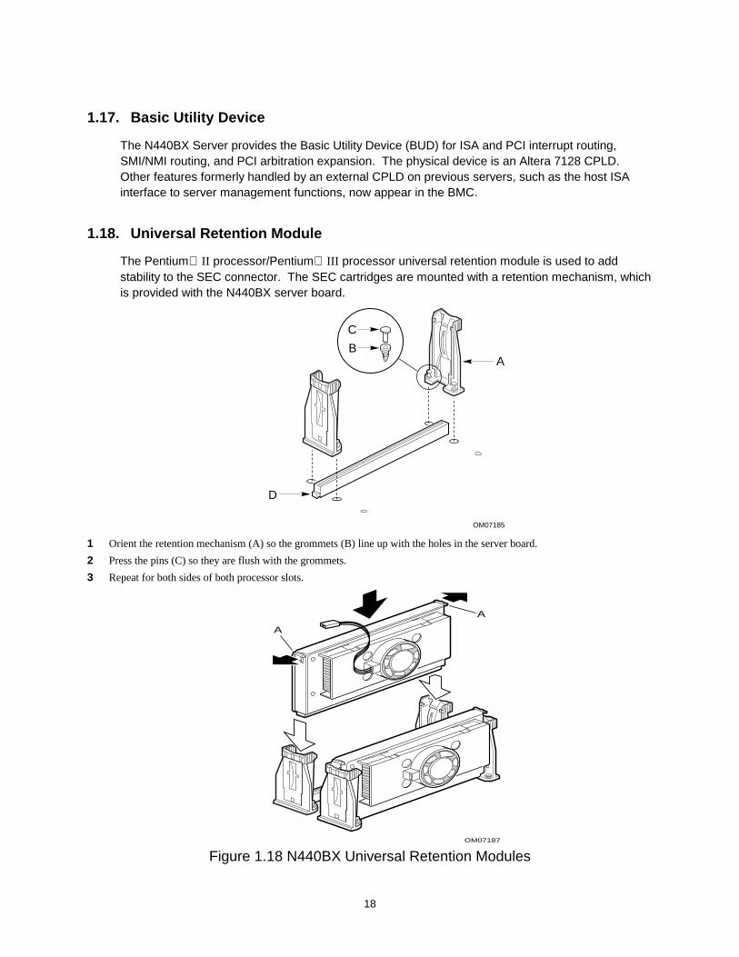
1.18. Universal Retention Module
The Pentium II processor/Pentium III processor universal retention module is used to addstability to the SEC connector. The SEC cartridges are mounted with a retention mechanism, whichis provided with the N440BX server board.
D
OM07185
A
C
B
1 Orient the retention mechanism (A) so the grommets (B) line up with the holes in the server board.
2 Press the pins (C) so they are flush with the grommets.
3 Repeat for both sides of both processor slots.
A
A
OM07187
Figure 1.18 N440BX Universal Retention Modules
19
1.18.1. Cartridge ConnectorThe Pentium® II processor/Pentium® III processor SEC connector conforms to the “Slot 1”specification, which can also accommodate future processor SEC cartridges. The baseboardprovides two SEC/SECC2 cartridge connectors. Processors and Slot 1 connectors are keyed toensure proper orientation.
1.18.2. Processor Heat/Fan SinksThe N440BX Server baseboard is not dependent on having fansinks. The term “fansinks” comesfrom the fan assembly that attaches to the SEC cartridge. The use of the fansink is not required,unless the thermal characteristics of the chassis require extra cooling. For the proper cooling ofthe processor please refer to the Pentium II processor and Pentium III processor specifications.
1.19. Processor Bus Termination/Regulation/Power
The termination circuitry required by the Pentium II processor/Pentium III processor bus (GTL+)signaling environment and the circuitry to set the GTL+ reference voltage, are implemented directlyon the SEC or SECC2 cartridges. The baseboard provides 1.5V GTL+ termination power (VTT),and VRM 8.1-compliant DC-to-DC converters to provide processor power (VCCP) at eachconnector. Power for primary processor is derived from the +12V supply, and the secondaryprocessor utilizes the +5V supply using an embedded DC-DC converter onboard. Both VRM’s areon the baseboard.
1.20. Termination Card
Logic is provided on the baseboard to detect the presence and identity of installed processor ortermination cards. If only one Pentium II processor or Pentium III processor is installed in asystem, a termination card must be installed in the vacant SEC connector to ensure reliable systemoperation. The termination card contains GTL+ termination circuitry, clock signal termination, andTest Access Port (TAP) bypassing for the vacant connector.
The board will not boot if a termination card is not installed in the vacant slot.
1.21. Functional Architecture
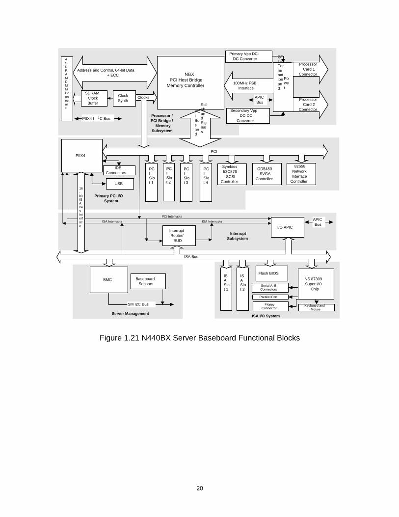
The following diagram illustrates the functional architecture of the N440BX Server baseboard, withdotted lines showing major functional blocks. This chapter describes the operation of each blockand associated circuitry. In addition, this chapter provides high level descriptions of functionalitydistributed between functional blocks (e.g., interrupt structure, clocks, resets, and servermanagement).
20
PIIX4
I/O APIC
BMC
PCI
Symbios53C876
SCSIControllerUSB
IDEConnectors
ISASlot 2
NS 87309Super I/O
ChipSerial A, BConnectors
Parallel Port
FloppyConnector
Keyboard andMouse
Flash BIOSBaseboard
Sensors
NBXPCI Host Bridge
Memory Controller
PCIBusand
SidebandSignals
4SDRAMDIMMConnectors
Clocks
Address and Control, 64-bit Data+ ECC
Processor /PCI Bridge /
MemorySubsystem
ISA Bus
Server ManagementISA I/O System
Primary PCI I/OSystem
GTL+Terminationand
Power
ProcessorCard 1
Connector
ProcessorCard 2
Connector
100MHz FSBInterface
PIIX4 I 2C Bus
PCISlot 1
PCISlot 2
PCISlot 3
Secondary VppDC-DC
Converter
APICBus
APICBus
Primary Vpp DC-DC Converter
ClockSynth
PCISlot 4
SDRAMClockBuffer
GD5480SVGA
Controller
82558NetworkInterface
Controller
SM I2C Bus
ISASlot 1
InterruptRouter/
BUD
ISA InterruptsISA Interrupts
PCI Interrupts
InterruptSubsystem
16-bitISABusInterface
Figure 1.21 N440BX Server Baseboard Functional Blocks
21
1.22. Processor/PCI Host Bridge/Memory Subsystem
The processor/PCI bridge/memory subsystem consists of support for one to two identical Pentium®II processor or Pentium® III processor cartridges, and up to four SDRAM DIMMs. This supportcircuitry on the baseboard consists of the following:
• Intel 440BX (NBX) PCI host bridge, memory, and power management2 controller chip.
• Dual 100MHz system bus Slot 1 edge connectors that accept identical processor cards (if using1 processor, a GTL+ terminator card goes in the empty slot).
• Four 168-pin DIMM connectors for interface to SDRAM memory.
• Processor host bus GTL+ support circuitry, including termination power supply.
• Embedded DC-to-DC voltage converters for processor power.
• APIC bus.
• Miscellaneous logic for reset configuration, processor card presence detection, and ITP port.
1.22.1. N440BX Host Bridge The NBX is a BGA device with a 3.3V core and mixed 5V, 3.3V, and GTL+ signal interface pins.The PCI host bridge in the NBX provides the sole pathway between processor and I/O systems,performing control signal translations and managing the data path in transactions with PCIresources onboard. This includes translation of 64-bit operations in the GTL+ signalingenvironment at 100MHz, to a 32-bit PCI Rev. 2.1 compliant, 5V signaling environment at 33MHz.The NBX also handles arbitration for PCI bus master access. For more information on N440BXServer arbitration specifics, refer to “PCI Arbitration” later in this chapter. Although the NBX iscapable of being clocked to operate with multiple processor system bus frequencies, on N440BXServer the host bridge only supports a 100MHz system bus. The device also features 32-bitaddressing (not 36-bit), 4 or 1 deep in-order and request queue (IOQ), dynamic deferred transactionsupport, and Desktop Optimized (DTO) GTL bus driver support (gated transceivers for reducedpower operation). The PCI interface provides greater than 100 MB/s data streamlining for PCI toSDRAM accesses (120 MB/s for writes), while supporting concurrent processor host bus and PCItransactions to main memory. This is accomplished using extensive data buffering, with processor-to-SDRAM and PCI-to-SDRAM write data buffering and write-combining support for processor-to-PCI burst writes.
1.22.2. N440BX Memory Controller The N440BX performs the function of memory controller for N440BX Server. Total memory of32MB to 256MB per DIMM is supported. Although the memory controller supports a variety ofmemory devices, the N440BX Server implementation only supports PC/100 compliant, 72-bit,unbuffered or registered SDRAM DIMMs. For complete information on supported devices, refer tothe PC/100 SDRAM Specification, 4-Clock 100MHz 64-bit and 72-bit Unbuffered SDRAM DIMM,and 4-Clock 100MHz 64-bit and 72-bit Unbuffered SDRAM DIMM documents.
2 Refer to “Power Management” later in this chapter, for information on how NBX and PIIX4 power managementfeatures are used on N440BX Server.
22
The N440BX provides ECC that can detect and correct single-bit errors (SED/SEC), and detect alldouble-bit and some multiple-bit errors (DED). Parity checking and ECC can be configured undersoftware control; higher performance is possible if ECC is disabled (1 clock savings). At initialpower-up, ECC and parity checking are disabled.
1.22.3. SDRAM Memory DIMM Sites N440BX Server provides 4 connectors that accept 168-pin JEDEC, 3.3V, 72-bit unbuffered orregistered SDRAM DIMMs. You cannot use EDO DIMMs, only SDRAM DIMMs are allowed. Youcan mix various sizes of DIMMs, mixing unbuffered and registered DIMMs is not allowed. Bestperformance is obtained using unbuffered DIMMs. Registered DIMMs stack memory devices oneach DIMM for greater memory capacity, but they require additional time (1 clock) for memoryaccesses.
CAUTION, single-processor configurations If you install only one processor in a system, it must go in the primary connector (closest to theDIMM sockets and the center of the server board). With a single-processor configuration, you mustinstall a termination board and termination latch assembly in the empty secondary connector(closest to the edge of the server board) to ensure proper operation of your system. A terminationboard is provided with the N440BX server board.
OM07188
A
B
Figure 1.23 N440BX Server Baseboard Termination Card
1.23. APIC Bus
Interrupt notification and generation for the dual processors is done using an independent pathbetween local APICs in each processor and the Intel I/O APIC located on the baseboard. Thissimple bus consists of 2 data signals and one clock line. PC-compatible interrupt handling is doneby the PIIX4, with all interrupts delivered to the processor via the INTR line. However, reducedinterrupt latency is possible when the APIC bus delivers interrupts in uni-processor operation (ifsupported by the OS).
23
1.24. Miscellaneous Processor/Memory Subsystem Circuitry
In addition to the circuitry described above, the processor subsystem contains the following:
• Processor core frequency configuration circuitry
• DIMM presence detection and auto-configuration logic
• Processor card presence detection circuitry
• ITP port for boundary scan support.
1.25. Processor Core Frequency and Memory Configuration Logic
The PIIX4 provides an independent IMB segment, the PIIX4 System Management Bus (PIIX4SMB), supporting an IMB EEMUX device (PCF8550) for configuration of processor core speed.The PIIX4 IMB segment also provides access to information stored in IMB ROMs on installedDIMMs, and control of the SDRAM clock buffer that gates synchronous clocks to each DIMM. Thisfeature allows a defective DIMM to be disabled, and total memory resized automatically. BIOS codecontrols these features using IMB operations performed by the PIIX4. Refer to “ServerManagement”, for a description of the other two IMB segments on N440BX Server, and informationon how the PIIX4 SMB fits into the overall server management scheme.
1.26 Processor Card Presence Detection
Logic is provided on the baseboard to detect the presence and identity of installed processor ortermination cards. A termination card must be installed in a vacant processor card slot to ensurereliable system operation. If the logic senses an empty connector, the system will not power up,preventing operation of the system with an improperly terminated GTL+ processor bus.
1.27. PCI I/O Subsystem
All I/O for N440BX Server, including PCI and PC-compatible, is directed through the PCI interface.On N440BX Server, the PCI bus supports the following embedded devices and connectors:
• Four 120-pin, 32-bit, 5 Volt, PCI expansion slot connectors, one is Intelligent I/O (I2O) ready
• PIIX4 PCI-to-ISA bridge / IDE / USB / Power Management (and PIIX4 SMB) controller
• PCI video controller, Cirrus Logic CL-GD5480
• PCI Ultra SCSI Controller, Symbios Logic SYM53C876
• PCI Network Interface Controller, Intel 82558
Each device under the PCI host bridge has its IDSEL signal connected to one bit out of the PCIAddress/Data lines AD[31::11], which acts as a device select on the PCI bus. This determines aunique PCI device ID value for use in configuration cycles. The following table shows the bit towhich each IDSEL signal is attached, along with its corresponding device number.
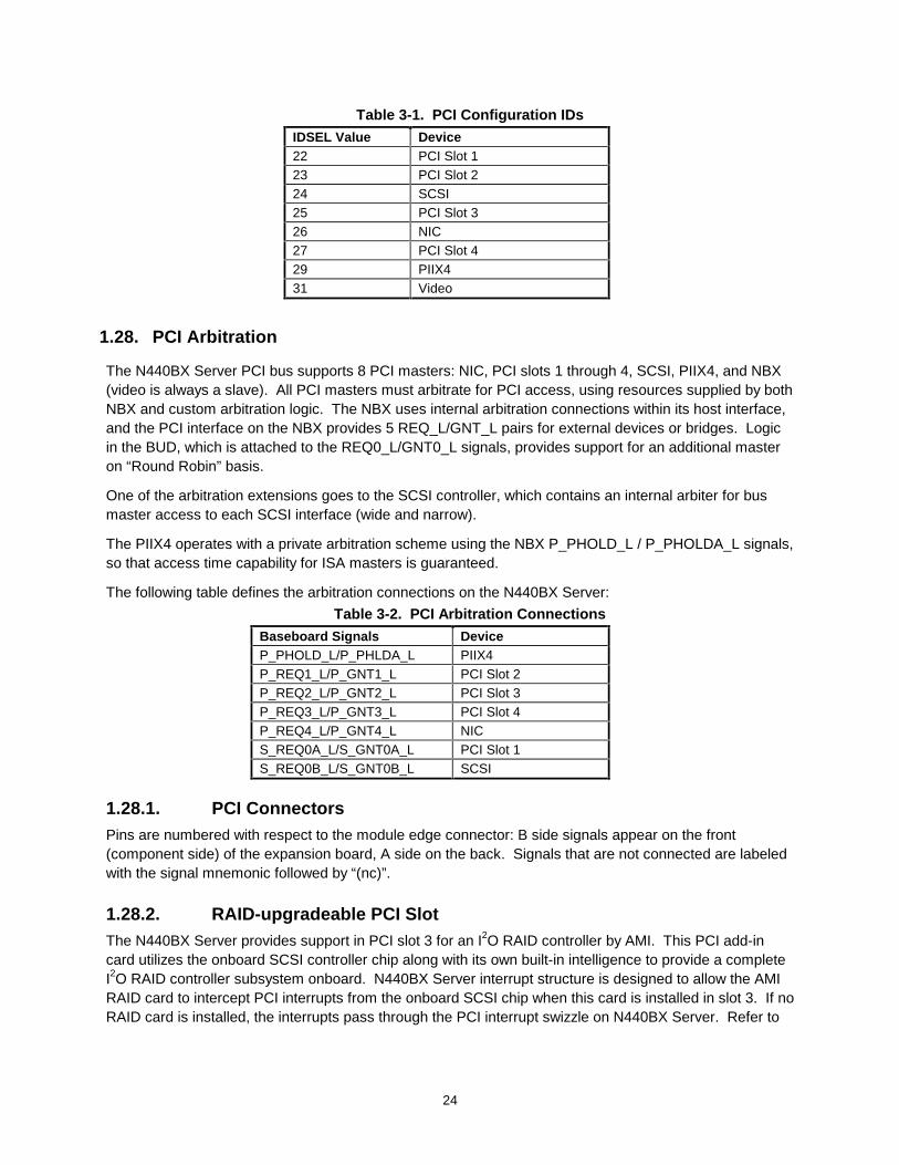
24
Table 3-1. PCI Configuration IDs
IDSEL Value Device 22 PCI Slot 1 23 PCI Slot 2 24 SCSI 25 PCI Slot 3 26 NIC 27 PCI Slot 4 29 PIIX4 31 Video
1.28. PCI Arbitration
The N440BX Server PCI bus supports 8 PCI masters: NIC, PCI slots 1 through 4, SCSI, PIIX4, and NBX(video is always a slave). All PCI masters must arbitrate for PCI access, using resources supplied by bothNBX and custom arbitration logic. The NBX uses internal arbitration connections within its host interface,and the PCI interface on the NBX provides 5 REQ_L/GNT_L pairs for external devices or bridges. Logicin the BUD, which is attached to the REQ0_L/GNT0_L signals, provides support for an additional masteron “Round Robin” basis.
One of the arbitration extensions goes to the SCSI controller, which contains an internal arbiter for busmaster access to each SCSI interface (wide and narrow).
The PIIX4 operates with a private arbitration scheme using the NBX P_PHOLD_L / P_PHOLDA_L signals,so that access time capability for ISA masters is guaranteed.
The following table defines the arbitration connections on the N440BX Server:
Table 3-2. PCI Arbitration Connections
Baseboard Signals Device P_PHOLD_L/P_PHLDA_L PIIX4 P_REQ1_L/P_GNT1_L PCI Slot 2 P_REQ2_L/P_GNT2_L PCI Slot 3 P_REQ3_L/P_GNT3_L PCI Slot 4 P_REQ4_L/P_GNT4_L NIC S_REQ0A_L/S_GNT0A_L PCI Slot 1 S_REQ0B_L/S_GNT0B_L SCSI
1.28.1. PCI Connectors Pins are numbered with respect to the module edge connector: B side signals appear on the front(component side) of the expansion board, A side on the back. Signals that are not connected are labeledwith the signal mnemonic followed by “(nc)”.
1.28.2. RAID-upgradeable PCI Slot The N440BX Server provides support in PCI slot 3 for an I2O RAID controller by AMI. This PCI add-incard utilizes the onboard SCSI controller chip along with its own built-in intelligence to provide a completeI2O RAID controller subsystem onboard. N440BX Server interrupt structure is designed to allow the AMIRAID card to intercept PCI interrupts from the onboard SCSI chip when this card is installed in slot 3. If noRAID card is installed, the interrupts pass through the PCI interrupt swizzle on N440BX Server. Refer to
25
“Interrupts and I/O APIC” later in this chapter for more information on N440BX Server interrupt structure.Refer to the AMI Web site for details on the RAID card.
1.28.3. PCI Bus Termination Certain PCI signals on N440BX Server have “functional” termination, i.e., either pull-up or pull-downresistors. In addition, certain PCI signals may require additional termination to meet signal qualityrequirements. These are driven through the board topology definition and simulation process, and are notspecified in this document. The table in the appendix describes functional termination for PCI signals onN440BX Server. ACK64_L, PRSNT1_L, PRSNT2_L, REQ_L, REQ64_L, SBO_L, SDONE, and TRST_Lare terminated at each PCI device and slot. All other signals listed in the table below are bussed, andrequire only a single pull-up or pull-down resistor. This also applies to the boundary scan signals TCK,TDI, and TMS which are unused in the system (TDO is unterminated).
The N440BX Server implementation of TRST_L does not follow the PCI guideline, but instead implementsa more robust solution by providing individual pull-down resistors for each slot. This is done tocompensate for numerous PCI components that violate the PCI input low leakage current (Iil)specification. If an add-in card directly connects the TRST_L pin on one of these components to the PCIconnector, the system would not work with that card installed if the TRST_L signals were bussed and thestandard pull-down guideline were used.
SBO_L and SDONE are unused on N440BX Server, but have separate pull-up resistors for each slot perthe PCI specification. PRSNT1_L and PRSNT2_L are also not used, and are terminated on eachconnector with 0.1µF caps to ground on each slot. ACK64_L and REQ64_L have pull-up resistors since64-bit PCI is not supported on N440BX Server. REQ_L for each slot also has a separate pull-up resistorsince these signals are not bussed. Note that REQ_L from onboard PCI components do not require pull-up resistors since they are always driven.
1.29. PIIX4
The PIIX4 is a multi-function PCI device, providing four PCI functions in a single package: PCI-to-ISAbridge, PCI IDE interface, PCI USB controller, and power management controller. Each function withinthe PIIX4 has its own set of configuration registers and once configured, each appears to the system as adistinct hardware controller sharing the same PCI bus interface. Refer to “Accessing ConfigurationSpace” for more information on programming configuration space for multi-function devices.
The PIIX4 on N440BX Server primary role is to provide the gateway to all PC-compatible I/O devices andfeatures. N440BX Server uses the following PIIX4 features:
• PCI interface
• ISA bus interface
• Dual IDE interfaces
• Power management control
• System reset control
• ISA-compatible interrupt control
• PC-compatible timer/counters and DMA controllers
• Baseboard plug-n-play support

26
• General purpose I/O
• Real-time Clock and CMOS configuration RAM.
Following are descriptions of each supported PIIX4 feature on the N440BX Server, and relatedconnector pinouts.
1.29.1. PIIX4 PCI Interface The PIIX4 fully implements a 32-bit PCI master/slave interface, in accordance with the PCI LocalBus Specification, Rev. 2.1. On the N440BX Server, the PCI interface operates at 33 MHz, using a5V signaling environment.
1.29.2. ISA Interface Function 0 in the PIIX4 provides an ISA bus interface, operating at 8.33 MHz, that supports two ISAexpansion connectors, Flash memory, server management interface, and the SuperI/O chip(PC87309VLJ). Refer to “ISA I/O Subsystem”, later in this chapter, for more information.
1.29.3. PCI Bus Master IDE Interface Function 1 in the PIIX4 provides a PCI bus master controller for dual IDE channels, each capable ofprogrammed I/O (PIO) operation for transfer rates up to 14 MB/s, and Ultra DMA operation fortransfer rates up to 33 MB/s. Each IDE channel supports two drives (0 and 1). Two IDEconnectors, each featuring 40 pins (2 x 20), are provided on the baseboard, pinout is specified inthe appendix. Unused signals are labeled with the signal mnemonic followed by the N440BX Serverimplementation in parentheses: “p/u” = pull-up resistor, “nc” = no connection.
1.29.4. Power Management Controller One of the embedded functions in the PIIX4 is a power management controller. On N440BXServer, power management features are obtained using ACPI-compatible software control. For acomplete discussion of power management architecture on N440BX Server, refer to “PowerManagement” later in this chapter.
1.29.5. Compatibility Interrupt Control The PIIX4 provides the functionality of two 82C59 PIC devices, for ISA-compatible interrupthandling. For a complete discussion of interrupt handling on N440BX Server, refer to “Interruptsand I/O APIC” later in this chapter.
1.29.6. Real-time Clock The PIIX4 contains an MC14681A compatible real-time clock with battery backup from an externalbattery. The device also contains 242 bytes of general purpose battery backed CMOS systemconfiguration RAM. On N440BX Server, these functions are duplicated in the SuperI/O chip.However, the N440BX Server implementation uses the PIIX4 RTC and CMOS facilities.
1.29.7. General Purpose Input and Output Pins The PIIX4 provides a number of general purpose input and output pins. Some of the pins aremultiplexed with specific signals and are unavailable as GPIOs, and some perform dedicated GPIOfunctions on N440BX Server, as shown in the following table.
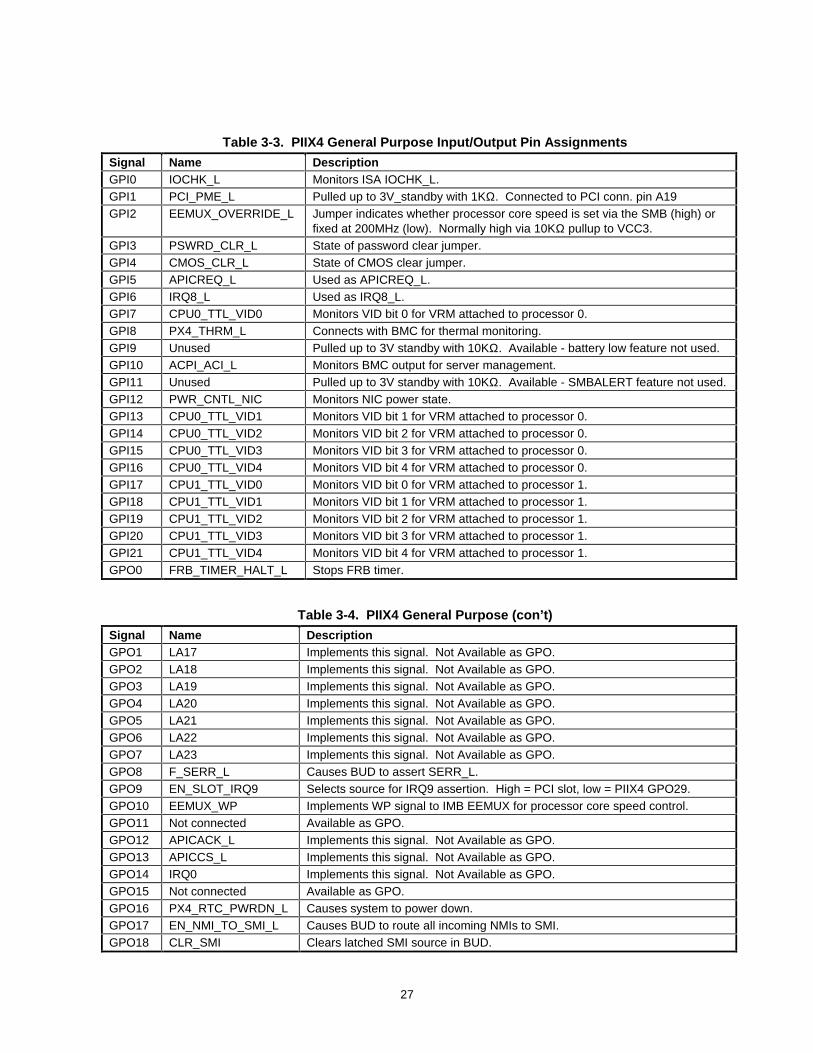
27
Table 3-3. PIIX4 General Purpose Input/Output Pin Assignments
Signal Name Description GPI0 IOCHK_L Monitors ISA IOCHK_L. GPI1 PCI_PME_L Pulled up to 3V_standby with 1KΩ. Connected to PCI conn. pin A19 GPI2 EEMUX_OVERRIDE_L Jumper indicates whether processor core speed is set via the SMB (high) or
fixed at 200MHz (low). Normally high via 10KΩ pullup to VCC3. GPI3 PSWRD_CLR_L State of password clear jumper. GPI4 CMOS_CLR_L State of CMOS clear jumper. GPI5 APICREQ_L Used as APICREQ_L. GPI6 IRQ8_L Used as IRQ8_L. GPI7 CPU0_TTL_VID0 Monitors VID bit 0 for VRM attached to processor 0. GPI8 PX4_THRM_L Connects with BMC for thermal monitoring. GPI9 Unused Pulled up to 3V standby with 10KΩ. Available - battery low feature not used. GPI10 ACPI_ACI_L Monitors BMC output for server management. GPI11 Unused Pulled up to 3V standby with 10KΩ. Available - SMBALERT feature not used. GPI12 PWR_CNTL_NIC Monitors NIC power state. GPI13 CPU0_TTL_VID1 Monitors VID bit 1 for VRM attached to processor 0. GPI14 CPU0_TTL_VID2 Monitors VID bit 2 for VRM attached to processor 0. GPI15 CPU0_TTL_VID3 Monitors VID bit 3 for VRM attached to processor 0. GPI16 CPU0_TTL_VID4 Monitors VID bit 4 for VRM attached to processor 0. GPI17 CPU1_TTL_VID0 Monitors VID bit 0 for VRM attached to processor 1. GPI18 CPU1_TTL_VID1 Monitors VID bit 1 for VRM attached to processor 1. GPI19 CPU1_TTL_VID2 Monitors VID bit 2 for VRM attached to processor 1. GPI20 CPU1_TTL_VID3 Monitors VID bit 3 for VRM attached to processor 1. GPI21 CPU1_TTL_VID4 Monitors VID bit 4 for VRM attached to processor 1. GPO0 FRB_TIMER_HALT_L Stops FRB timer.
Table 3-4. PIIX4 General Purpose (con’t)
Signal Name Description GPO1 LA17 Implements this signal. Not Available as GPO. GPO2 LA18 Implements this signal. Not Available as GPO. GPO3 LA19 Implements this signal. Not Available as GPO. GPO4 LA20 Implements this signal. Not Available as GPO. GPO5 LA21 Implements this signal. Not Available as GPO. GPO6 LA22 Implements this signal. Not Available as GPO. GPO7 LA23 Implements this signal. Not Available as GPO. GPO8 F_SERR_L Causes BUD to assert SERR_L. GPO9 EN_SLOT_IRQ9 Selects source for IRQ9 assertion. High = PCI slot, low = PIIX4 GPO29. GPO10 EEMUX_WP Implements WP signal to IMB EEMUX for processor core speed control. GPO11 Not connected Available as GPO. GPO12 APICACK_L Implements this signal. Not Available as GPO. GPO13 APICCS_L Implements this signal. Not Available as GPO. GPO14 IRQ0 Implements this signal. Not Available as GPO. GPO15 Not connected Available as GPO. GPO16 PX4_RTC_PWRDN_L Causes system to power down. GPO17 EN_NMI_TO_SMI_L Causes BUD to route all incoming NMIs to SMI. GPO18 CLR_SMI Clears latched SMI source in BUD.
28
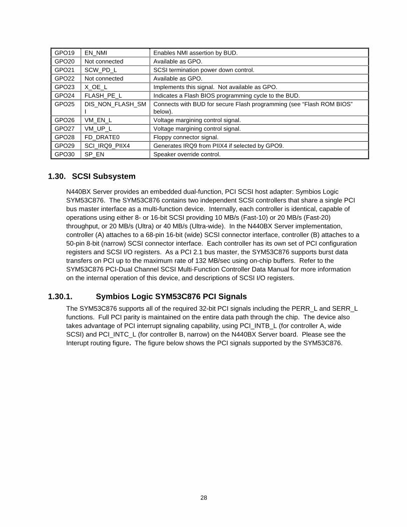
GPO19 EN_NMI Enables NMI assertion by BUD. GPO20 Not connected Available as GPO. GPO21 SCW_PD_L SCSI termination power down control. GPO22 Not connected Available as GPO. GPO23 X_OE_L Implements this signal. Not available as GPO. GPO24 FLASH_PE_L Indicates a Flash BIOS programming cycle to the BUD. GPO25 DIS_NON_FLASH_SM
I Connects with BUD for secure Flash programming (see “Flash ROM BIOS”below).
GPO26 VM_EN_L Voltage margining control signal. GPO27 VM_UP_L Voltage margining control signal. GPO28 FD_DRATE0 Floppy connector signal. GPO29 SCI_IRQ9_PIIX4 Generates IRQ9 from PIIX4 if selected by GPO9. GPO30 SP_EN Speaker override control.
1.30. SCSI Subsystem
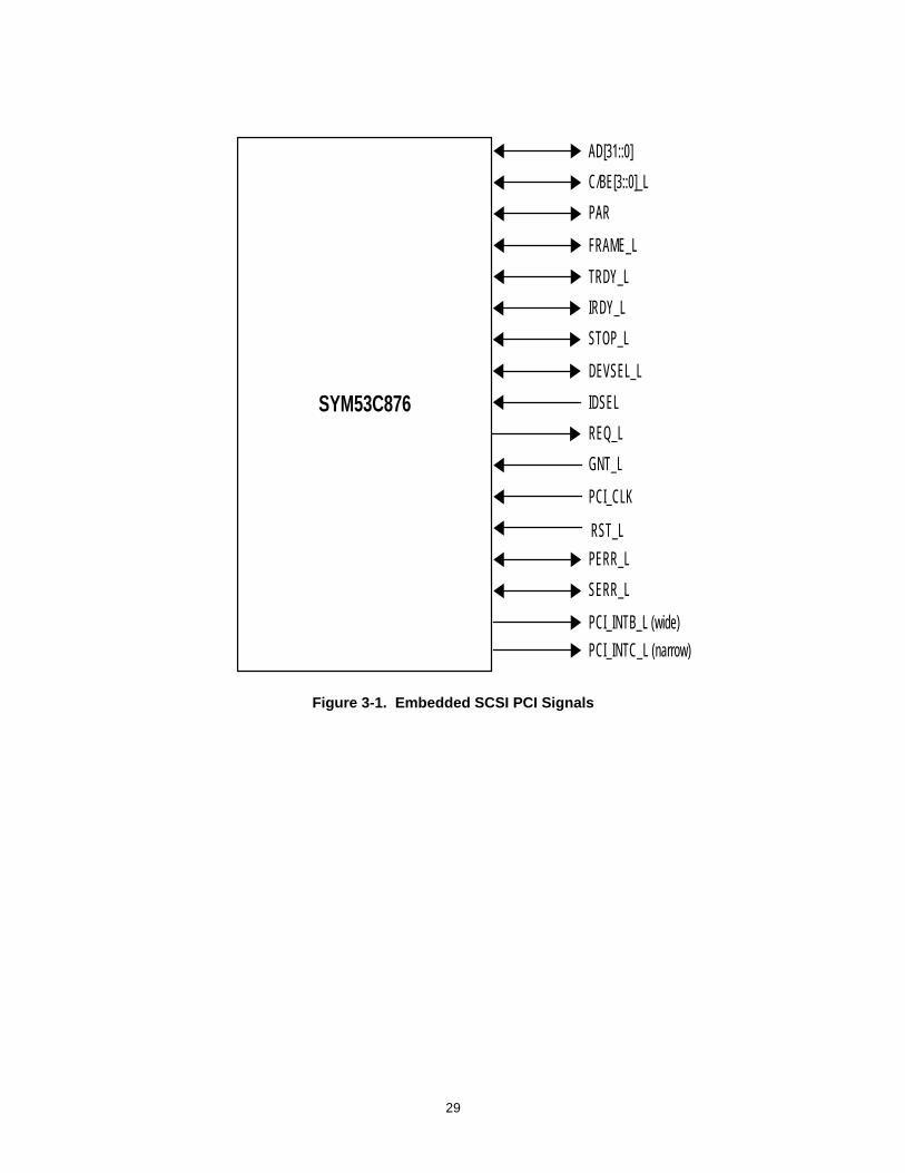
N440BX Server provides an embedded dual-function, PCI SCSI host adapter: Symbios LogicSYM53C876. The SYM53C876 contains two independent SCSI controllers that share a single PCIbus master interface as a multi-function device. Internally, each controller is identical, capable ofoperations using either 8- or 16-bit SCSI providing 10 MB/s (Fast-10) or 20 MB/s (Fast-20)throughput, or 20 MB/s (Ultra) or 40 MB/s (Ultra-wide). In the N440BX Server implementation,controller (A) attaches to a 68-pin 16-bit (wide) SCSI connector interface, controller (B) attaches to a50-pin 8-bit (narrow) SCSI connector interface. Each controller has its own set of PCI configurationregisters and SCSI I/O registers. As a PCI 2.1 bus master, the SYM53C876 supports burst datatransfers on PCI up to the maximum rate of 132 MB/sec using on-chip buffers. Refer to theSYM53C876 PCI-Dual Channel SCSI Multi-Function Controller Data Manual for more informationon the internal operation of this device, and descriptions of SCSI I/O registers.
1.30.1. Symbios Logic SYM53C876 PCI Signals The SYM53C876 supports all of the required 32-bit PCI signals including the PERR_L and SERR_Lfunctions. Full PCI parity is maintained on the entire data path through the chip. The device alsotakes advantage of PCI interrupt signaling capability, using PCI_INTB_L (for controller A, wideSCSI) and PCI_INTC_L (for controller B, narrow) on the N440BX Server board. Please see theInterupt routing figure. The figure below shows the PCI signals supported by the SYM53C876.
29
SYM53C876
PAR
STOP_L
TRDY_L
C/BE[3::0]_L
FRAME_L
AD[31::0]
SERR_L
PCI_CLK
RST_L
PERR_L
GNT_L
IRDY_L
DEVSEL_L
IDSEL
REQ_L
PCI_INTB_L (wide)
PCI_INTC_L (narrow)
Figure 3-1. Embedded SCSI PCI Signals
30
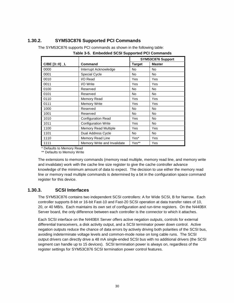
1.30.2. SYM53C876 Supported PCI Commands The SYM53C876 supports PCI commands as shown in the following table:
Table 3-5. Embedded SCSI Supported PCI Commands
SYM53C876 Support C/BE [3::0] _L Command Target Master
0000 Interrupt Acknowledge No No 0001 Special Cycle No No 0010 I/O Read Yes Yes 0011 I/O Write Yes Yes 0100 Reserved No No 0101 Reserved No No 0110 Memory Read Yes Yes 0111 Memory Write Yes Yes 1000 Reserved No No 1001 Reserved No No 1010 Configuration Read Yes No 1011 Configuration Write Yes No 1100 Memory Read Multiple Yes Yes 1101 Dual Address Cycle No No 1110 Memory Read Line Yes* Yes 1111 Memory Write and Invalidate Yes** Yes
* Defaults to Memory Read** Defaults to Memory Write
The extensions to memory commands (memory read multiple, memory read line, and memory writeand invalidate) work with the cache line size register to give the cache controller advanceknowledge of the minimum amount of data to expect. The decision to use either the memory readline or memory read multiple commands is determined by a bit in the configuration space commandregister for this device.
1.30.3. SCSI Interfaces The SYM53C876 contains two independent SCSI controllers: A for Wide SCSI, B for Narrow. Eachcontroller supports 8-bit or 16-bit Fast-10 and Fast-20 SCSI operation at data transfer rates of 10,20, or 40 MB/s. Each maintains its own set of configuration and run-time registers. On the N440BXServer board, the only difference between each controller is the connector to which it attaches.
Each SCSI interface on the N440BX Server offers active negation outputs, controls for externaldifferential transceivers, a disk activity output, and a SCSI terminator power down control. Activenegation outputs reduce the chance of data errors by actively driving both polarities of the SCSI bus,avoiding indeterminate voltage levels and common-mode noise on long cable runs. The SCSIoutput drivers can directly drive a 48 mA single-ended SCSI bus with no additional drivers (the SCSIsegment can handle up to 15 devices). SCSI termination power is always on, regardless of theregister settings for SYM53C876 SCSI termination power control features.
31
1.30.4. SCSI Bus The SCSI data bus is 8- or 16-bits wide with odd parity generated per byte. SCSI control signals arethe same for either bus width. To accommodate 8-bit devices on the 16-bit Wide SCSI connector,the SYM53C876 assigns the highest arbitration priority to the low byte of the 16-bit word. This way,16-bit targets can be mixed with 8-bit if the 8-bit devices are placed on the low data byte. For 8-bitmode, the unused high data byte is self-terminated and need not be connected. During chip powerdown, all inputs are disabled to reduce power consumption. Please see the Appendix for pin outs ofthe narrow and wide SCSI connectors.
1.31. PCI Video
N440BX Server provides a Cirrus Logic CL-GD5480 video controller, along with video SGRAM andsupport circuitry for an embedded SVGA video subsystem. The CL-GD5480 64-bit VGA GraphicsAccelerator chip contains an SVGA video controller, clock generator, BitBLT engine, and RAMDAC.256K x 32 SGRAM chips provide 2 MB (factory build option, no socket) of 10ns video memory. TheSVGA subsystem supports a variety of modes: up to 1600 x 1200 resolution, and up to 16.7 Mcolors. It also supports analog VGA monitors, single- and multi-frequency, interlaced and non-interlaced, up to 100 Hz vertical retrace frequency. The N440BX Server board also provides astandard 15 pin VGA connector, and external video blanking logic for server management consoleredirection support.
1.32. Video Chip PCI Signals
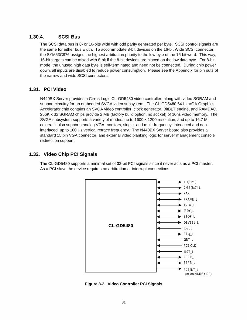
The CL-GD5480 supports a minimal set of 32-bit PCI signals since it never acts as a PCI master.As a PCI slave the device requires no arbitration or interrupt connections.
CL-GD5480
PAR
STOP_L
TRDY_L
C/BE[3::0]_L
FRAME_L
AD[31::0]
SERR_L
PCI_CLK
RST_L
PERR_L
GNT_L
IRDY_L
DEVSEL_L
IDSEL
REQ_L
PCI_INT_L (nc on N440BX DP)
Figure 3-2. Video Controller PCI Signals
32
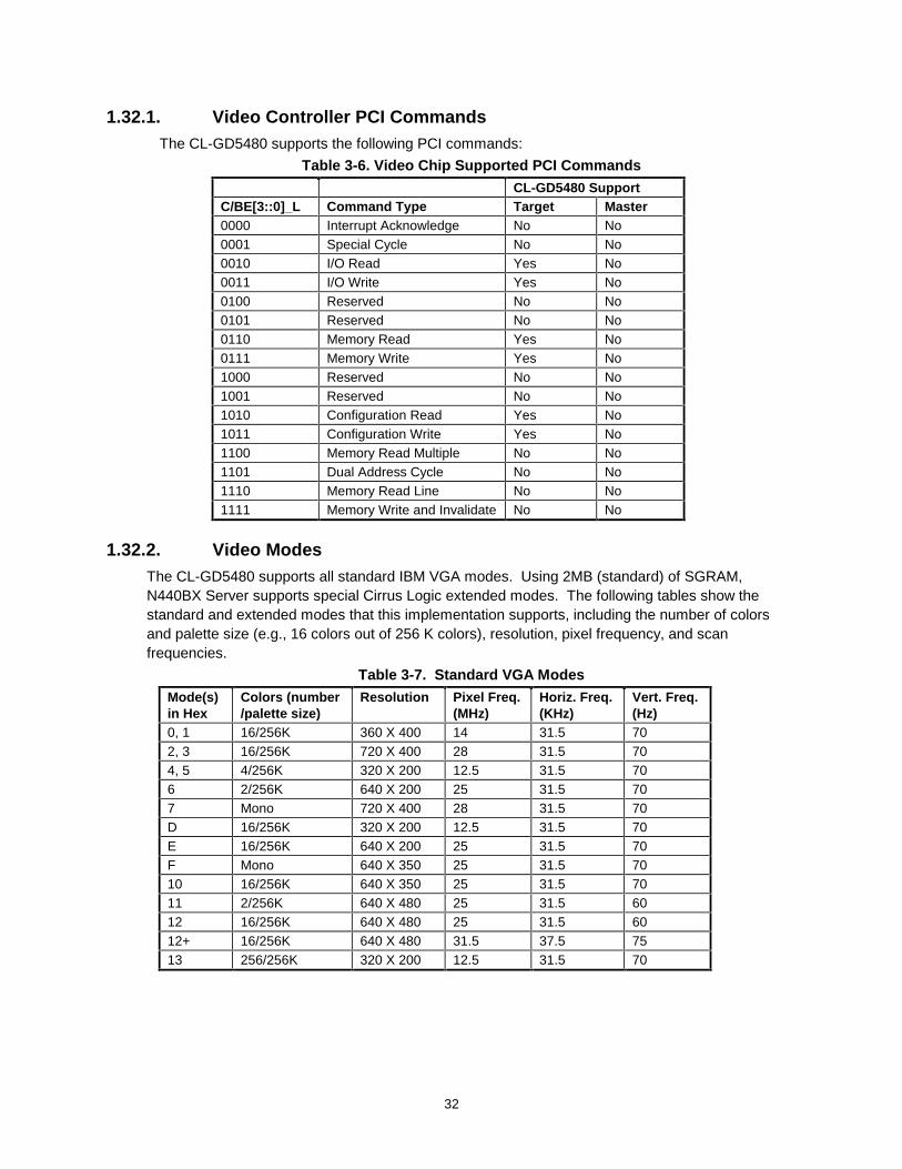
1.32.1. Video Controller PCI Commands The CL-GD5480 supports the following PCI commands:
Table 3-6. Video Chip Supported PCI Commands
CL-GD5480 Support C/BE[3::0]_L Command Type Target Master 0000 Interrupt Acknowledge No No 0001 Special Cycle No No 0010 I/O Read Yes No 0011 I/O Write Yes No 0100 Reserved No No 0101 Reserved No No 0110 Memory Read Yes No 0111 Memory Write Yes No 1000 Reserved No No 1001 Reserved No No 1010 Configuration Read Yes No 1011 Configuration Write Yes No 1100 Memory Read Multiple No No 1101 Dual Address Cycle No No 1110 Memory Read Line No No 1111 Memory Write and Invalidate No No
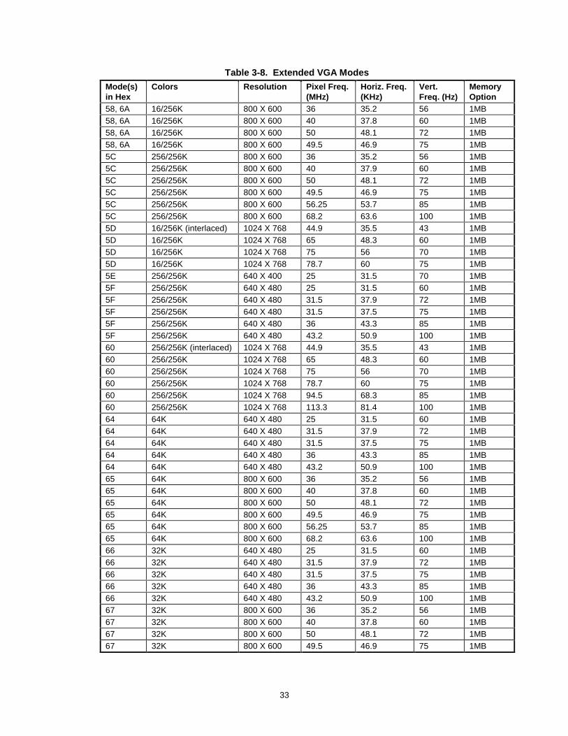
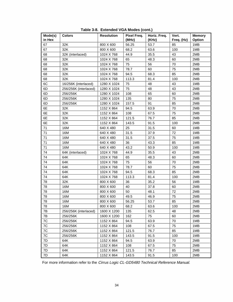
1.32.2. Video Modes The CL-GD5480 supports all standard IBM VGA modes. Using 2MB (standard) of SGRAM,N440BX Server supports special Cirrus Logic extended modes. The following tables show thestandard and extended modes that this implementation supports, including the number of colorsand palette size (e.g., 16 colors out of 256 K colors), resolution, pixel frequency, and scanfrequencies.
Table 3-7. Standard VGA Modes
Mode(s)in Hex
Colors (number/palette size)
Resolution Pixel Freq.(MHz)
Horiz. Freq.(KHz)
Vert. Freq.(Hz)
0, 1 16/256K 360 X 400 14 31.5 70 2, 3 16/256K 720 X 400 28 31.5 70 4, 5 4/256K 320 X 200 12.5 31.5 70 6 2/256K 640 X 200 25 31.5 70 7 Mono 720 X 400 28 31.5 70 D 16/256K 320 X 200 12.5 31.5 70 E 16/256K 640 X 200 25 31.5 70 F Mono 640 X 350 25 31.5 70 10 16/256K 640 X 350 25 31.5 70 11 2/256K 640 X 480 25 31.5 60 12 16/256K 640 X 480 25 31.5 60 12+ 16/256K 640 X 480 31.5 37.5 75 13 256/256K 320 X 200 12.5 31.5 70
33
Table 3-8. Extended VGA Modes
Mode(s)in Hex
Colors Resolution Pixel Freq.(MHz)
Horiz. Freq.(KHz)
Vert.Freq. (Hz)
MemoryOption
58, 6A 16/256K 800 X 600 36 35.2 56 1MB 58, 6A 16/256K 800 X 600 40 37.8 60 1MB 58, 6A 16/256K 800 X 600 50 48.1 72 1MB 58, 6A 16/256K 800 X 600 49.5 46.9 75 1MB 5C 256/256K 800 X 600 36 35.2 56 1MB 5C 256/256K 800 X 600 40 37.9 60 1MB 5C 256/256K 800 X 600 50 48.1 72 1MB 5C 256/256K 800 X 600 49.5 46.9 75 1MB 5C 256/256K 800 X 600 56.25 53.7 85 1MB 5C 256/256K 800 X 600 68.2 63.6 100 1MB 5D 16/256K (interlaced) 1024 X 768 44.9 35.5 43 1MB 5D 16/256K 1024 X 768 65 48.3 60 1MB 5D 16/256K 1024 X 768 75 56 70 1MB 5D 16/256K 1024 X 768 78.7 60 75 1MB 5E 256/256K 640 X 400 25 31.5 70 1MB 5F 256/256K 640 X 480 25 31.5 60 1MB 5F 256/256K 640 X 480 31.5 37.9 72 1MB 5F 256/256K 640 X 480 31.5 37.5 75 1MB 5F 256/256K 640 X 480 36 43.3 85 1MB 5F 256/256K 640 X 480 43.2 50.9 100 1MB 60 256/256K (interlaced) 1024 X 768 44.9 35.5 43 1MB 60 256/256K 1024 X 768 65 48.3 60 1MB 60 256/256K 1024 X 768 75 56 70 1MB 60 256/256K 1024 X 768 78.7 60 75 1MB 60 256/256K 1024 X 768 94.5 68.3 85 1MB 60 256/256K 1024 X 768 113.3 81.4 100 1MB 64 64K 640 X 480 25 31.5 60 1MB 64 64K 640 X 480 31.5 37.9 72 1MB 64 64K 640 X 480 31.5 37.5 75 1MB 64 64K 640 X 480 36 43.3 85 1MB 64 64K 640 X 480 43.2 50.9 100 1MB 65 64K 800 X 600 36 35.2 56 1MB 65 64K 800 X 600 40 37.8 60 1MB 65 64K 800 X 600 50 48.1 72 1MB 65 64K 800 X 600 49.5 46.9 75 1MB 65 64K 800 X 600 56.25 53.7 85 1MB 65 64K 800 X 600 68.2 63.6 100 1MB 66 32K 640 X 480 25 31.5 60 1MB 66 32K 640 X 480 31.5 37.9 72 1MB 66 32K 640 X 480 31.5 37.5 75 1MB 66 32K 640 X 480 36 43.3 85 1MB 66 32K 640 X 480 43.2 50.9 100 1MB 67 32K 800 X 600 36 35.2 56 1MB 67 32K 800 X 600 40 37.8 60 1MB 67 32K 800 X 600 50 48.1 72 1MB 67 32K 800 X 600 49.5 46.9 75 1MB
34
Table 3-8. Extended VGA Modes (cont.)
Mode(s)in Hex
Colors Resolution Pixel Freq.(MHz)
Horiz. Freq.(KHz)
Vert.Freq. (Hz)
MemoryOption
67 32K 800 X 600 56.25 53.7 85 1MB 67 32K 800 X 600 68.2 63.6 100 1MB 68 32K (interlaced) 1024 X 768 44.9 35.5 43 2MB 68 32K 1024 X 768 65 48.3 60 2MB 68 32K 1024 X 768 75 56 70 2MB 68 32K 1024 X 768 78.7 60 75 2MB 68 32K 1024 X 768 94.5 68.3 85 2MB 68 32K 1024 X 768 113.3 81.4 100 2MB 6C 16/256K (interlaced) 1280 X 1024 75 48 43 1MB 6D 256/256K (interlaced) 1280 X 1024 75 48 43 2MB 6D 256/256K 1280 X 1024 108 65 60 2MB 6D 256/256K 1280 X 1024 135 80 75 2MB 6D 256/256K 1280 X 1024 157.5 91 85 2MB 6E 32K 1152 X 864 94.5 63.9 70 2MB 6E 32K 1152 X 864 108 67.5 75 2MB 6E 32K 1152 X 864 121.5 76.7 85 2MB 6E 32K 1152 X 864 143.5 91.5 100 2MB 71 16M 640 X 480 25 31.5 60 1MB 71 16M 640 X 480 31.5 37.9 72 1MB 71 16M 640 X 480 31.5 37.5 75 1MB 71 16M 640 X 480 36 43.3 85 1MB 71 16M 640 X 480 43.2 50.9 100 1MB 74 64K (interlaced) 1024 X 768 44.9 35.5 43 2MB 74 64K 1024 X 768 65 48.3 60 2MB 74 64K 1024 X 768 75 56 70 2MB 74 64K 1024 X 768 78.7 60 75 2MB 74 64K 1024 X 768 94.5 68.3 85 2MB 74 64K 1024 X 768 113.3 81.4 100 2MB 78 32K 800 X 600 36 35.2 56 1MB 78 16M 800 X 600 40 37.8 60 2MB 78 16M 800 X 600 50 48.1 72 2MB 78 16M 800 X 600 49.5 46.9 75 2MB 78 16M 800 X 600 56.25 53.7 85 2MB 78 16M 800 X 600 68.2 63.6 100 2MB 7B 256/256K (interlaced) 1600 X 1200 135 62.5 48 2MB 7B 256/256K 1600 X 1200 162 75 60 2MB 7C 256/256K 1152 X 864 94.5 63.9 70 1MB 7C 256/256K 1152 X 864 108 67.5 75 1MB 7C 256/256K 1152 X 864 121.5 76.7 85 1MB 7C 256/256K 1152 X 864 143.5 91.5 100 1MB 7D 64K 1152 X 864 94.5 63.9 70 2MB 7D 64K 1152 X 864 108 67.5 75 2MB 7D 64K 1152 X 864 121.5 76.7 85 2MB 7D 64K 1152 X 864 143.5 91.5 100 2MB
For more information refer to the Cirrus Logic CL-GD5480 Technical Reference Manual.
35
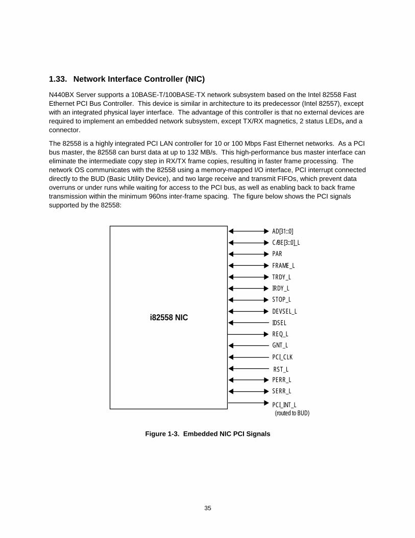
1.33. Network Interface Controller (NIC)
N440BX Server supports a 10BASE-T/100BASE-TX network subsystem based on the Intel 82558 FastEthernet PCI Bus Controller. This device is similar in architecture to its predecessor (Intel 82557), exceptwith an integrated physical layer interface. The advantage of this controller is that no external devices arerequired to implement an embedded network subsystem, except TX/RX magnetics, 2 status LEDs, and aconnector.
The 82558 is a highly integrated PCI LAN controller for 10 or 100 Mbps Fast Ethernet networks. As a PCIbus master, the 82558 can burst data at up to 132 MB/s. This high-performance bus master interface caneliminate the intermediate copy step in RX/TX frame copies, resulting in faster frame processing. Thenetwork OS communicates with the 82558 using a memory-mapped I/O interface, PCI interrupt connecteddirectly to the BUD (Basic Utility Device), and two large receive and transmit FIFOs, which prevent dataoverruns or under runs while waiting for access to the PCI bus, as well as enabling back to back frametransmission within the minimum 960ns inter-frame spacing. The figure below shows the PCI signalssupported by the 82558:
i82558 NIC
PAR
STOP_L
TRDY_L
C/BE[3::0]_L
FRAME_L
AD[31::0]
SERR_L
PCI_CLK
RST_L
PERR_L
GNT_L
IRDY_L
DEVSEL_L
IDSEL
REQ_L
PCI_INT_L (routed to BUD)
Figure 1-3. Embedded NIC PCI Signals
36
1.33.1. Supported Network Features The 82558 contains an IEEE MII compliant interface to the components necessary to implement a IEEE802.3 100BASE-TX network connection. N440BX Server supports the following features of the 82557controller:
• Glueless 32-bit PCI Bus Master Interface (Direct Drive of Bus), compatible with PCI BusSpecification, revision 2.1
• 82596-like chained memory structure, with improved dynamic transmit chaining for enhancedperformance
• Programmable transmit threshold for improved bus utilization
• Early receive interrupt for concurrent processing of receive data
• On-chip counters for network management
• Autodetect and autoswitching for 10 or 100 Mbps network speeds
• Support for both 10 Mbps and 100 Mbps Networks, full or half duplex-capable, with back-to-back transmit at 100 Mbps
• Integrated physical interface to TX magnetics.
The magnetics component terminates the 100BASE-TX connector interface. A Flash device storesthe network ID.
1.33.2. NIC Connector and Status LEDs The 82558 drives LEDs on the network interface connector that indicate transmit/receive activity on theLAN, valid link to the LAN, and 10/100 Mbps operation.
1.34. ISA I/O Subsystem
On the N440BX Server, the PIIX4 provides a bridge to an ISA I/O subsystem that supports the followingconnectors and devices:
• Two ISA slots, one physically shared with PCI slot 1
• Flash memory for BIOS ROM and extensions
• National Semiconductor PC87309VLJ SuperI/O chip, which supports the following:
• Two PC-compatible serial ports
• Enhanced parallel port
• Floppy controller
• Keyboard/Mouse ports
The ISA I/O subsystem also connects with the Intel I/O APIC and BMC. The I/O APIC relays interruptsproduced by ISA devices in dual processor operation (or in uni-processor operation for increasedperformance with certain OS implementations. The BUD, a programmable logic device performsrerouting of PCI interrupts as ISA interrupts for MP OS implementations that are not fully MPS 1.4compatible, and management interrupt (NMI_L and SMI_L) control. Refer to “Interrupts and I/O APIC”later in this chapter for more information on these devices and how they are used in the N440BX Serverinterrupt structure. The BMC controls server management features on N440BX Server. Refer to “Server
37
Management” later in this chapter for details. For details on pin out and termination please refer to theAppendix.
1.35. Compatibility I/O Controller Subsystem
The National PC87309VLJ SuperI/O device is a plug and play (PnP) compatible standard I/Osubsystem chip. This device contains all of the necessary circuitry to control two serial ports, oneparallel port, floppy disk, and PS/2-compatible keyboard and mouse. N440BX Server provides theconnector interface for each. In addition, the SuperI/O contains a real-time clock, which is unusedon N440BX Server.
Note:
Unlike it predecessor (87307), the PC87309VLJ provides no general purpose I/O bits orprogrammable chip selects. All GPIOs required by N440BX Server subsystems are supplied by thePIIX4 as specified above.
1.36.1. Serial Ports Two connectors are provided, one 9-pin D-Sub in the stacked housing for Serial port A, and thesecond via 10-pin header for Serial port B. Both ports are compatible with 16550A and 16450UARTs, supporting relocatable I/O addresses. Each serial port can be set to 1 of 4 different COMports, and can be enabled separately. When enabled, each port can be programmed to generateedge or level sensitive interrupts. When disabled, serial port interrupts are available to add-incards. The pinout for the two connectors are available in the appendix.
1.36.2. Parallel Port The 25/15 pin high rise connector stacks the parallel port connector over the VGA and serial Port Aconnector. The 87309 provides an IEEE 1284-compliant 25-pin bi-directional parallel port. BIOSprogramming of the SuperI/O registers enable the parallel port, and determine the port address andinterrupt. When disabled, the interrupt is available to add-in cards. Pin out of the Parallel port isavailable in the appendix.
1.36.3. Floppy Disk Controller The FDC on the SuperI/O is functionally compatible with the PC8477, which contains a superset ofthe floppy disk controllers in the DP8473 and N82077. The baseboard provides the 24 MHz clock,termination resistors, and chip selects. All other FDC functions are integrated into the SuperI/O,including analog data separator and 16-byte FIFO. Pinout is available in the appendix.
1.36.4. Keyboard and Mouse Connectors The keyboard and mouse connectors are mounted within a single stacked housing. The mouseconnector is stacked over the keyboard connector. External to the board they appear as twoconnectors. The keyboard and mouse controller are software compatible with the 8042AH andPC87911. The keyboard and mouse connectors are PS/2 compatible, with pinout available in theappendix.
38
1.36.5. Front Panel Header (AT, System) An inline AT header is provided for AT-style front panel connections, e.g., power, LED indicators,and reset as well has a Front panel 2x16 post socket header. Both pin outs are available in theappendix.
1.36.6. Flash ROM BIOS An 8Mbit flash memory (Intel 28F008S5) provides non-volatile storage space for BIOS and generalpurposes. The device is byte wide, of the Smart 5 FlashFile family and symmetrically blocked. TheFlash device is directly addressed as 16 64-kbyte blocks of 8-bit ISA memory. Refer to the Byte-Wide Smart 5 FlashFile Memory Family 4, 8, and 16 MB Data Book for additional deviceinformation.
1.36.7. Secure Flash Programming Mechanism On N440FX DP, the BUD detects any write operation to Flash and asserts SMI_L. The SMI_Lhandler (part of BIOS) then looks for a signature from the Flash Memory Update utility (FMUP)before allowing any writes to Flash. This prevents accidental loading of non-compatible BIOS codeinto Flash.
1.37. System Reset Control
Reset circuitry on the N440BX Server board monitors reset from the front panel, PIIX4, I/Ocontroller, and processor subsystem to determine proper reset sequencing for all types of reset.The reset logic is designed to accommodate a variety of ways to reset the system, which can bedivided into the following categories:
• Power-up reset
• Hard reset
• Soft (programmed) reset
1.37.1. Power-up Reset Power-up reset occurs on the initial application of power to the system. The power supply assertsits "power good" signal within 400 to 2000ms of its output voltages being stable. The BMC monitorsthis signal, and asserts its power good output 30 to 40ms after detecting the power supply’s powergood signal asserted (the onboard VRMs are designed to provide stable processor power 30 to40ms after the main power is stable).
1.37.2. Hard Reset Hard reset may be initiated by software, or by the user resetting the system through the front panel.For software initiated hard reset, the PIIX4 Reset Control register should be used. The front panelreset is routed to the PIIX4 through the reset and power micro-controller. Both sources of hardreset cause the PIIX4 to assert ISA bus reset (RST_RSTDRV) and PCI reset (RST_P_RST_LB).RST_RSTDRV resets the ISA subsystem, while RST_P_RST_L resets the PCI bus. The NBXreceives the PCI reset signal and propagates it to the processor subsystem
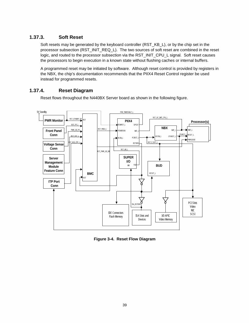
39
1.37.3. Soft Reset Soft resets may be generated by the keyboard controller (RST_KB_L), or by the chip set in theprocessor subsection (RST_INIT_REQ_L). The two sources of soft reset are combined in the resetlogic, and routed to the processor subsection via the RST_INIT_CPU_L signal. Soft reset causesthe processors to begin execution in a known state without flushing caches or internal buffers.
A programmed reset may be initiated by software. Although reset control is provided by registers inthe NBX, the chip’s documentation recommends that the PIIX4 Reset Control register be usedinstead for programmed resets.
1.37.4. Reset Diagram Reset flows throughout the N440BX Server board as shown in the following figure.
NBX
RSTIN_L CPURST_L
INIT_L
IDE ConnectorsFlash Memory
ISA_RSTDRV
RST_P_RST_L
PIIX4
POWEROK
RCIN_L PCIRST_L
RSTDRV
INIT_L
SUPERI/O
MR P20
RST_KB_L
Processor(s)
RESET_L
INIT_L
CPURST_L
RST_OC_INIT_CPU_LRST_STNDBY_FP
RST_FP_L
PWR_GD_PS
RST_SFC_L
5V Standby FRB_TIMERHALT_L
RST_PWR_GD_BB
GPO21
RST
RST_PIIX4_L
RST
Front PanelConn
ServerManagement
ModuleFeature Conn
PWR Monitor
Voltage SenseConn
ITP Port Conn
RST_REQ_ITP_L
RSMRST_L
BMC
BUD
RESET_L
PWRGOOD
ISA Slots andDevices
PCI SlotsVideoNIC
SCSII/O APICVideo Memory
Figure 3-4. Reset Flow Diagram
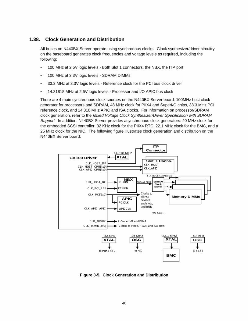
40
1.38. Clock Generation and Distribution
All buses on N440BX Server operate using synchronous clocks. Clock synthesizer/driver circuitryon the baseboard generates clock frequencies and voltage levels as required, including thefollowing:
• 100 MHz at 2.5V logic levels - Both Slot 1 connectors, the NBX, the ITP port
• 100 MHz at 3.3V logic levels - SDRAM DIMMs
• 33.3 MHz at 3.3V logic levels - Reference clock for the PCI bus clock driver
• 14.31818 MHz at 2.5V logic levels - Processor and I/O APIC bus clock
There are 4 main synchronous clock sources on the N440BX Server board: 100MHz host clockgenerator for processors and SDRAM, 48 MHz clock for PIIX4 and SuperI/O chips, 33.3 MHz PCIreference clock, and 14.318 MHz APIC and ISA clocks. For information on processor/SDRAMclock generation, refer to the Mixed Voltage Clock Synthesizer/Driver Specification with SDRAMSupport. In addition, N440BX Server provides asynchronous clock generators: 40 MHz clock forthe embedded SCSI controller, 32 KHz clock for the PIIX4 RTC, 22.1 MHz clock for the BMC, and a25 MHz clock for the NIC. The following figure illustrates clock generation and distribution on theN440BX Server board.
CLK_APIC_CPU[1::0]
CLK_APIC_APIC
CLK_PCI_REF
CLK_HOST_CPU[1::0]
CLK_HOST_BX
CLK_HOST_ITP
to NICto PIIX4 RTC
CK100 DriverSlot 1 Conns.
CLK_APICCLK_HOST
ITPConnector
Clocks toall PCIdevicesand slots,and BUD
NBXHCLKIN
PCLKIN
APIC
APICCLK
PCICLK
BMC
XTALXTAL32 KHz
XTAL14.318 MHz
CLK_PCI[6::0]Memory DIMMs
SDRAM_CLKS
CLK_HOST_SDRAM[15::0]
CLK_48MHZ to Super I/O and PIIX4
CLK_14MHZ[3::0] Clocks to Video, PIIX4, and ISA slots
22.1 MHz
SDRAMClockBuffer
40 MHz
OSC
25 MHz
OSC25 MHz
to SCSI
Figure 3-5. Clock Generation and Distribution
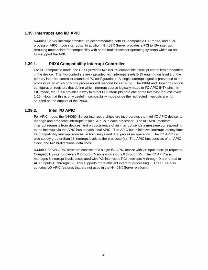
41
1.39. Interrupts and I/O APIC
N440BX Server interrupt architecture accommodates both PC-compatible PIC mode, and dual-processor APIC mode interrupts. In addition, N440BX Server provides a PCI to ISA interruptrerouting mechanism for compatibility with some multiprocessor operating systems which do notfully support the APIC.
1.39.1. PIIX4 Compatibility Interrupt ControllerFor PC-compatible mode, the PIIX4 provides two 82C59-compatible interrupt controllers embeddedin the device. The two controllers are cascaded with interrupt levels 8-15 entering on level 2 of theprimary interrupt controller (standard PC configuration). A single interrupt signal is presented to theprocessors, to which only one processor will respond for servicing. The PIIX4 and SuperI/O containconfiguration registers that define which interrupt source logically maps to I/O APIC INTx pins. InPIC mode, the PIIX4 provides a way to direct PCI interrupts onto one of the interrupt request levels1-15. Note that this is only useful in compatibility mode since the redirected interrupts are notsourced on the outputs of the PIIX4.
1.39.2. Intel I/O APICFor APIC mode, the N440BX Server interrupt architecture incorporates the Intel I/O APIC device, tomanage and broadcast interrupts to local APICs in each processor. The I/O APIC monitorsinterrupt requests from devices, and on occurrence of an interrupt sends a message correspondingto the interrupt via the APIC bus to each local APIC. The APIC bus minimizes interrupt latency timefor compatibility interrupt sources, in both single and dual processor operation. The I/O APIC canalso supply greater than 16 interrupt levels to the processor(s). The APIC bus consists of an APICclock, and two bi-directional data lines.
N440BX Server APIC structure consists of a single I/O APIC device with 24 input interrupt requests.Compatibility interrupt levels 0 through 15 appear on inputs 0 through 15. The I/O APIC alsomanages 8 interrupt levels associated with PCI interrupts: PCI interrupts A through D are routed toAPIC inputs 16 through 19. This supports more efficient interrupt processing. The PIIX4 alsocontains I/O APIC features that are not used in the N440BX Server platform.
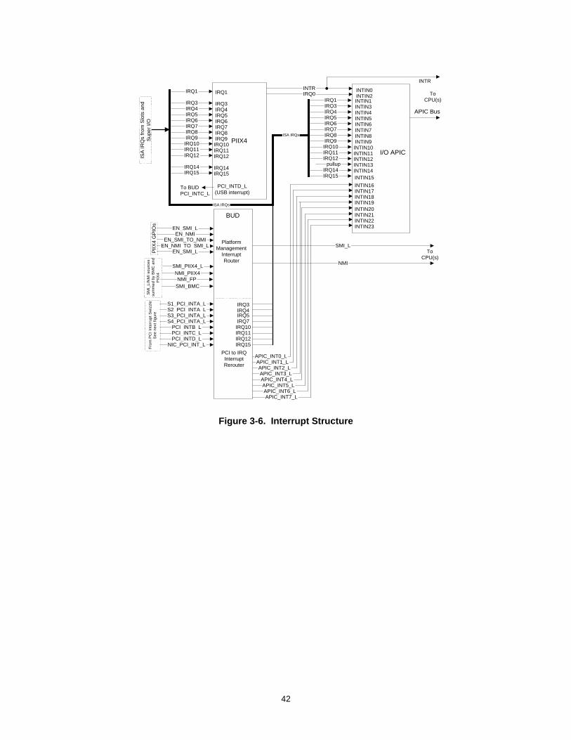
42
PIIX4
IRQ1
BUD
S1_PCI_INTA_L
S4_PCI_INTA_L
IRQ1
IRQ3IRQ4IRQ5IRQ6IRQ7IRQ8IRQ9
IRQ10IRQ11IRQ12
IRQ14IRQ15
PCI_INTD_L(USB interrupt)
IRQ3IRQ4IRQ5IRQ6IRQ7IRQ8IRQ9
IRQ10IRQ11IRQ12
IRQ15IRQ14
IRQ0 INTIN2
IRQ3IRQ4IRQ5IRQ6IRQ7IRQ8IRQ9IRQ10IRQ11IRQ12
IRQ15IRQ14
IRQ1 INTIN1
INTR INTIN0
INTIN4INTIN5
INTIN3
INTIN7INTIN8
INTIN6
INTIN10INTIN11
INTIN9
INTIN12INTIN13INTIN14INTIN15
pullup
INTIN17INTIN18
INTIN16
INTIN19
INTIN21INTIN22
INTIN20
INTIN23
APIC_INT7_LAPIC_INT6_L
APIC_INT5_LAPIC_INT4_LAPIC_INT3_L
IRQ3IRQ4IRQ5IRQ7
IRQ12
IRQ10IRQ11
IRQ15
APIC_INT2_LAPIC_INT1_L
APIC_INT0_L
S2_PCI_INTA_LS3_PCI_INTA_L
PCI_INTB_LPCI_INTC_LPCI_INTD_L
NIC_PCI_INT_L
Fro
m P
CI
Inte
rrup
t S
wiz
zle
See
nex
t fig
ure
EN_SMI_L
EN_NMI_TO_SMI_L
EN_NMIEN_SMI_TO_NMI
SMI_PIIX4_L
SMI_BMCNMI_FP
NMI_PIIX4
EN_SMI_L
PCI to IRQInterruptRerouter
PlatformManagement
InterruptRouter
SMI_L
NMI
ToCPU(s)
ToCPU(s)
APIC Bus
INTR
PIIX
4 G
PIO
sI/O APIC
ISA IRQs
ISA IRQs
To BUDPCI_INTC_L
SM
I_L/
NM
I so
urce
ssu
mm
ed
by
BM
C a
nd
PIIX
4
ISA
IRQ
s fr
om S
lots
and
Sup
er I/
O
Figure 3-6. Interrupt Structure
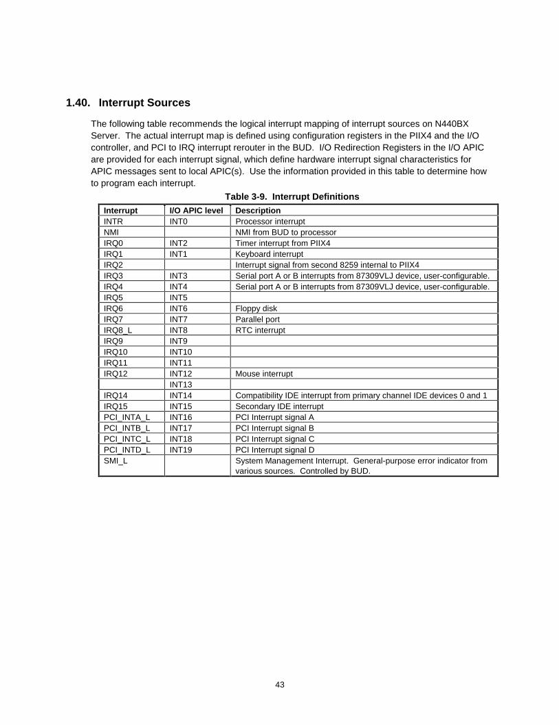
43
1.40. Interrupt Sources
The following table recommends the logical interrupt mapping of interrupt sources on N440BXServer. The actual interrupt map is defined using configuration registers in the PIIX4 and the I/Ocontroller, and PCI to IRQ interrupt rerouter in the BUD. I/O Redirection Registers in the I/O APICare provided for each interrupt signal, which define hardware interrupt signal characteristics forAPIC messages sent to local APIC(s). Use the information provided in this table to determine howto program each interrupt.
Table 3-9. Interrupt Definitions
Interrupt I/O APIC level DescriptionINTR INT0 Processor interruptNMI NMI from BUD to processorIRQ0 INT2 Timer interrupt from PIIX4IRQ1 INT1 Keyboard interruptIRQ2 Interrupt signal from second 8259 internal to PIIX4IRQ3 INT3 Serial port A or B interrupts from 87309VLJ device, user-configurable.IRQ4 INT4 Serial port A or B interrupts from 87309VLJ device, user-configurable.IRQ5 INT5IRQ6 INT6 Floppy diskIRQ7 INT7 Parallel portIRQ8_L INT8 RTC interruptIRQ9 INT9IRQ10 INT10IRQ11 INT11IRQ12 INT12 Mouse interrupt
INT13IRQ14 INT14 Compatibility IDE interrupt from primary channel IDE devices 0 and 1IRQ15 INT15 Secondary IDE interruptPCI_INTA_L INT16 PCI Interrupt signal APCI_INTB_L INT17 PCI Interrupt signal BPCI_INTC_L INT18 PCI Interrupt signal CPCI_INTD_L INT19 PCI Interrupt signal DSMI_L System Management Interrupt. General-purpose error indicator from
various sources. Controlled by BUD.
44
1.40.1. PCI Add-in Card Slot Interrupt SharingThe following figure shows how PCI interrupts, shared between slots and embedded controllers, arerouted to the BUD. The BUD manages each PCI_INT_A from each slot, cascaded PCI_INTs B through Cfrom each slot, and PCI interrupts from SCSI and NIC devices, to avoid conflicts (since most PCI cardsuse PCI_INTA_L as their interrupt pin). The arrows indicate the direction of interrupt flow from slot to slot,with final destination at the BUD interrupt inputs. The BUD then delivers each interrupt to the appropriatePIIX4 compatibility IRQ and I/O APIC INTIN pins.
*PCISlot 2
NIC PCIInterrupt
Wide SCSI PCIInterrupt C
S1_PCI_INT_A
PCI_INT_B
PCI_INT_C
PCI_INT_D
PCISlot 1
A
B
C
D
A
B
C
D
PCISlot 3
A
B
C
D
PCISlot 4
A
B
C
D
Narrow SCSIPCI Interrupt B
S2_PCI_INT_A
S3_PCI_INT_A
S4_PCI_INT_A
NIC_PCI_INT
BUD
Slot 3RAID-upgradeable PCI slot
Figure 3-7. PCI Slot Interrupt Swizzle
1.40.2. PCI Interrupt ReroutingSome multiprocessor operating systems are unable to handle interrupts from PCI slots and devices aspure PCI interrupts, via inputs 16-19 (allocated to PCI) of the I/O APIC. Rather, they expect PCI interruptsto be delivered as ISA IRQs. Multiprocessor operating systems may also expect some interrupts from thePC-compatible PIC in the PIIX4, and others from the I/O APIC (Mixed Mode). Some device drivers checkwhether the device uses one of the traditional IRQs, and if not (when the PCI interrupt is connecteddirectly to the I/O APIC), the driver fails to install or run properly. The PIIX4 performs internal PCI to IRQinterrupt steering so that PCI interrupts can be delivered to the PIC. However, the PCI interrupt steeringfeature is unidirectional, which means that it cannot redirect PCI interrupts to the I/O APIC.
For these reasons, N440BX Server incorporates an external PCI to IRQ rerouter circuit in the BUD, thatcan be programmed to pass PCI interrupts through to inputs 16-19 of the I/O APIC, or deliver a specificPCI interrupt to an ISA IRQ. Under software control, a PCI interrupt can be individually rerouted to an ISAIRQ signal. This functionality is contained in the BUD.
Two 8-bit registers are provided in the rerouter circuit, with each nibble of a register controlling a specificPCI Interrupt line via PIO commands. The PIIX4 decodes the address of the PIO command and producesa chip select, which is controlled using the PIIX4 Programmable Chip Select Control register (78h - 79h).The rerouter uses only 2 bytes of the minimum 4 selectable, so aliases are provided. Refer to “PCIInterrupt to IRQ Routing Control” for run-time programming information. Refer to PIIX4 ProgrammableChip Select Control register description for initialization-time requirements.
45
1.40.3. Working with PCI InterruptsThe N440BX DP Server baseboard shares PCI bus resources with onboard devices. The list below givessome guidelines to reduce the possibility of conflicts and performance restrictions.
1) Try to stay away from installing a LAN adapter in Slot 3. Either the configuration may not workor it may reduce the performance quality on the network. If the server needs an additional LANadapter, install it in Slot 1 or 2 and this will allow for maximum throughput. Slot 4 could have thesame results as Slot 3 and should not be used if possible
2) When configuring a RAID controller in the N440BX Server baseboard, Slots 1 and 2 are betterfor performance and configuration. This is due to the onboard resources that are being used.Another consideration is to have this RAID pack as the boot device. (Refer to Table 14 BootOrder.)
When integrating peripherals into a server system, taking into consideration the architecture of the PCIbus and the onboard resources can help in making the right choices and offering a reliable server.
1.41. Boot Order
The baseboard boot order for non-multi-boot cards is outlined in the following table. On the N440BXServer baseboard multi-boot cards will always sign-on ahead of all other cards and onboard SCSI.
Table 1 Boot Order
Order Boot Device
1 Onboard IDE
2 Onboard SCSI
3 PCI Slot 1
4 PCI Slot 2
5 PCI Slot 3
6 PCI Slot 4
1.42. System Management Interrupt Handling
N440BX Server is designed to report these types of system errors: ISA bus, PCI bus, ECC memory,and System limit. Errors are reported by the BMC and PIIX4 using SMI_L. SMI is used for servermanagement and advanced error processing. All errors can be intercepted by SMI forpreprocessing (if SMI_L is enabled), or handled directly by NMI handlers. Some errors have togenerate an NMI even if they are intercepted by the SMI, because the traditional way to handleerrors in PC architecture is via the NMI. NMI/SMI handling logic in the BUD emulates non-ISAerrors as ISA-compatible using NMI and SMI_L.
1.43. Basic Utility Device (BUD)
In addition to the PCI arbitration and interrupt rerouting functions described above, the BUD alsogates and redirects SMI_L and NMI to generate SERR_L, and performs other miscellaneous logic

46
functions (e.g., PCI arbitration expansion). The BUD contains an I/O mapped ISA interface forcontrol of PCI-to-IRQ interrupt rerouting. Functional specifications for BUD signal pins are given inthe following table.
47
Table 3-10. BUD Signal Descriptions
Signal Pin Type*
Description
AD0 92 I Driven by ISA address bit SA0.AD1 93 I Driven by ISA address bit SA1.APIC_INT0_L 32 O INT0 signal to I/O APIC via series 10Ω resistor.APIC_INT1_L 30 O INT1 signal to I/O APIC via series 10Ω resistor.APIC_INT2_L 31 O INT2 signal to I/O APIC via series 10Ω resistor.APIC_INT3_L 7 O INT3 signal to I/O APIC via series 10Ω resistor.APIC_INT4_L 33 O INT4 signal to I/O APIC via series 10Ω resistor.APIC_INT5_L 40 O INT5 signal to I/O APIC via series 10Ω resistor.APIC_INT6_L 9 O INT6 signal to I/O APIC via series 10Ω resistor.APIC_INT7_L 5 O INT7 signal to I/O APIC via series 10Ω resistor.BMC_SUSCLK 85 O BMC suspend clock. The BUD divides the 32KHz
PX4_SUSCLK (pin 41) by 256 to generate BMC_SUSCLKfor BMC timestamping of SM events.
CLK_APIC 29 I APIC clock from CK100 driverCLK_PCI_BUD 90 I Synchronous PCI master clock from CK100 driverCLR_SMI 61 I Driven by a PIIX4 GPIO bit 18 to clear a latched SMI
condition. On assertion, clears the latched SMI signal in theBUD.
CPU_NMI 69 O NMI to the processor(s), asserted when EN_NMI (pin 46)and NMI_PIIX4 (pin 50) are asserted, or when the FrontPanel NMI switch is pressed.
CPU_SMI_L 83 O Generates an SMI_L to the processor(s). This signal isgated by EN_SMI_L (pin 35) assertion and pending NMIrequest.
D0 94 I/O Connects to ISA bus data bit SD0.D1 96 I/O Connects to ISA bus data bit SD1.D2 97 I/O Connects to ISA bus data bit SD2.D3 98 I/O Connects to ISA bus data bit SD3.D4 99 I/O Connects to ISA bus data bit SD4.D5 100 I/O Connects to ISA bus data bit SD5.D6 1 I/O Connects to ISA bus data bit SD6.D7 2 I/O Connects to ISA bus data bit SD7.DIS_NON_FLASH_SMI
8 I Driven by PIIX4 GPIO bit 25 as part of secure Flashprogramming mechanism.
EN_NMI 46 I Driven by PIIX4 GPIO bit 19 to gate NMI generation (otherthan Front Panel NMI).
EN_NMI_TO_SMI_L 36 I Driven by PIIX4 GPIO bit 17 to redirect NMI to SMI.EN_SMI_L 35 I Driven by PIIX4 GPIO bit 9, to enable the generation of SMI
to the processor(s).EN_SMI_TO_NMI 62 I Driven by the BMC to redirect SMI_L to NMI, which is
controlled from the ISA interface using BMC mailboxregisters. SMI_L redirection occurs by default.
F_SERR 54 I Driven by PIIX4 GPIO bit 8 to force assertion of SERR_L onPCI. The BUD converts the signal to a pulse synchronouswith PCI, which generates SERR_L.
* I = Input, O = Output
48
Table 3-10. BUD Signal Descriptions (cont.)Signal Pin Typ
e*Description
FLASH_PE_L 48 I Driven by PIIX4 GPIO bit 24 to indicate a Flash BIOS programming cycle.The BUD generates SMI_L in response, which supports the secure Flashprogramming mechanism on N440BX DP (see “Flash ROM BIOS” above).
IORD_L 87, 14 I I/O read command driven by the ISA IORD_L signal.IOWR_L 10 I I/O write command driven by the ISA IOWC_L signal.IRQ3 12 O ISA IRQ3 signal from PCI to IRQ re-router in the BUD.IRQ4 68 O ISA IRQ4 signal from PCI to IRQ re-router in the BUD.IRQ5 13 O ISA IRQ5 signal from PCI to IRQ re-router in the BUD.IRQ7 44 O ISA IRQ7 signal from PCI to IRQ re-router in the BUD.IRQ10 65 O ISA IRQ10 signal from PCI to IRQ re-router in the BUD.IRQ11 67 O ISA IRQ11 signal from PCI to IRQ re-router in the BUD.IRQ12 49 O ISA IRQ12 signal from PCI to IRQ re-router in the BUD.IRQ15 64 O ISA IRQ15 signal from PCI to IRQ re-router in the BUD.ISA_BALE 72 I Driven by ISA BALE signal.ISA_RSTDRV_L 88 I Reset to the BUD from ISA interface reset signal.NMI_FP_L 42 I Front Panel NMI directly from the momentary push button switch on the
Front Panel (in parallel with BMC connection). Pressing of this switch iscaptured by NMI latch circuitry in the BUD.
NMI_PIIX4 50 I NMI indication from the PIIX4, which causes the assertion of CPU_NMI(pin 69) to occur if EN_NMI (pin 46) is also asserted.
P_GNT0_L 25 I GNT0_L signal from NBX for arbitration expansion logic in BUDP_INT_B_L 19 I Interrupt B from cascaded PCI_INTB,C,D_L PCI slot interrupt swizzle, and
SCSI controller PCI_INTB_L (wide).P_INT_C_L 18 I Interrupt C from cascaded PCI_INTB,C,D_L PCI slot interrupt swizzle, and
SCSI controller PCI_INTC_L (narrow).P_INT_D_L 17 I Interrupt D from cascaded PCI_INTB,C,D_L PCI slot swizzle.P_INT_NIC_L 20 I Interrupt from NIC PCI_INTA_LP_INT_PCI1_L 24 I Interrupt from PCI slot 1 PCI_INTA_LP_INT_PCI2_L 23 I Interrupt from PCI slot 2 PCI_INTA_LP_INT_PCI3_L 22 I Interrupt from PCI slot 3 PCI_INTA_LP_INT_PCI4_L 21 I Interrupt from PCI slot 4 PCI_INTA_LP_REQ0_L 79 O REQ_L signal to NBX from PCI arbitration logic expansion logic in BUD.P_SERR_L 80 O PCI SERR_L signal forced by the BUD.PD_CS_L 57 I Driven by PIIX4 PCS0 as part of ISA I/O interface to the BUD.PS_FRAME_L 37 I FRAME_L signal from PCI interface for arbitration expansion logic in BUD.PS_IRDY_L 55 I IRDY_L signal from PCI interface for arbitration expansion logic in BUD.PS_STOP_L 6 I STOP_L signal from PCI interface for arbitration expansion logic in BUD.PS_TRDY_L 52 I TRDY_L signal from PCI interface for arbitration expansion logic in BUD.PX4_SUSCLK 41 I PIIX4 suspend clock. 32KHz clock source for BMC suspend clock.RST_P_RST_L 89 I Reset to the BUD from PCI interface reset signal.S_GNT0A_L 71 O GNT_L signal to PCI slot 1S_GNT0B_L 84 O GNT_L signal to SCSI controller chipS_REQ0A_L 45 I REQ_L signal from PCI slot 1S_REQ0B_L 47 I REQ_L signal from SCSI controller chipSMI_BMC_L 27 I Driven by the BMC to indicate the occurrence of an SMI condition.SMI_PIIX4_L 56 I Asserted by the PIIX4 on occurrence of an SMI_L condition, to indicate a
request for handler service.TCK 62 I/O

49
Signal Pin Type*
Description
TDI 4 I/O IEEE 1149.1 Boundary Scan SignalsTDO 73 I/O (for prototype only)TMS 15 I/O
* I = Input, O = Output
50
2. Server Management
2.1. Overview
On N440BX Server, three serial buses that follow IMB protocol provide independent pathways forserver management functions. The PIIX4 system management bus mentioned above (PIIX4 SMB)connects with each DIMM, and controls SDRAM clocks and processor speed configuration. Asingle micro-controller referred to as the Baseboard Management Controller (BMC) manages theother two IMB segments:
• Server Management Bus supporting 8K SEEPROM and processor/baseboard temperaturesensors.
• Intelligent Management Bus (IMB) supporting connectors to system-wide server managementdevices.
In addition, the BMC manages sensors directly using I/O and ADC lines, controls the EmergencyManagement Port (EMP), detects and reports system fan failures, and manages Fault ResilientBooting (FRB). The BMC provides the Host ISA and IMB interfaces to server managementfeatures on N440BX Server. The following diagram illustrates server management architecture onthe N440BX Server baseboard.
BASEBOARDPROCESSOR SLOTS
Power Button Front Panel NMI
Reset Button Chassis Intrusion
SMSI/F
ISA BUS NMI
PIIX4 NMI
PIIX4 SMI
I/O and ADC Lines
BMC SMI
INTELLIGENT
MANAGEMENTBU
Auxiliary I2CConnector
SMM CardConnector
PowerConnector
To PowerShareBoard
Front Panel Connector
ServerManagementBus
RAM
Flash Memoryfor BMC
ProgrammingCode
16K
48K
SMI
Platform Mgt.Interrupt Router
in BUD
Non-volatile, read-write storage
SENSORDATA
RECORDS
SYSTEMEVENT
LOG
FRU INFO& CONFIG
DEFAULTS
8K SEEPROM
SMM-BIOS
I/F
ISOL
BASEBOARDMANAGEMENTCONTROLLER
(BMC)
ISA I/FPORTS
Front PanelControl
D101NIC
Baseboard TempSensor 2
SCSI-W Term.
FANs (2)
12V
-12V
IERR 1,2
Thermal Trip (2)
CPU Voltage (2)
CPU enable/disable (2)
GTL 1.5V
Chipset 2.5V
CPU1 Temp
CPU2 TempBaseboard Temp
Sensor 1
FANs (2)
COM2
COMMMUX
BBD COM2
ISOL
-5V
5V
3.3V
PIIX4
DIMM 3
DIMM 2
CPU Speed Set
SDRAM ClockBuffer
DIMM 1
DIMM 4
PIIX4 SM Bus
EMP
Figure 2-1. Server Management Block Diagram

51
2.2. Server Management Bus
The Server Management Bus (SMB) is a single master, open-drain, serial bus which is electricallyand timing compatible with the 100 Kbps version of the IMB bus specification. The SMB extendsthroughout the baseboard providing an independent pathway for the BMC to communicate with 2baseboard and 2 processor slot temperature sensors. In addition, the SMB supports an 8KSEEPROM device for non-volatile storage of the System Event Log (SEL), Sensor Data RecordRepository (SDRR), FRU information, and configuration defaults. The BMC controls access to thisdevice and manages the data structures within (refer to BMC description below).
Buffers are provided to isolate the baseboard and processor temperature sensors from the rest ofthe SMB. These buffers, running on 5V_Standby, keep the bus alive to the BMC even though mainpower is switched off. This allows the BMC to communicate with its SEEPROM at all times.
2.3. Intelligent Management Bus
The Intelligent Management Bus (IMB) is a multi-master, open-drain, serial bus which is alsoelectrically and timing compatible with the 100 Kbps version of the IMB bus specification. The IMBattaches to connectors on the baseboard creating a server management network that extendsthroughout the baseboard and system chassis, providing an independent pathway forcommunications between the BMC and system-level server management devices (e.g., Hot-swapSCSI controller). In addition, the IMB provides inter-chassis communications extensions for acomplete server management network solution.
The communication protocol for the IMB is defined in the Intelligent Management BusCommunications Protocol Specification. The protocol is designed to work with micro-controllers andother IMB masters, and slave devices such as IMB temperature sensors.
The IMB attaches to the following connector interfaces on the N440BX Server board:
• Auxiliary IMB connector
• Server Monitor Module (SMM) card feature connector
• Front panel connector
• Auxiliary power connector (via isolation buffer)
The N440BX Server board provides the main pull-ups on the clock (IMB_SCL) and data (IMB_SDA)lines of the IMB. This termination is sized to drive the full IMB, i.e., capacitive loading for not onlythe board, but for the chassis, SMM Card IMB, and auxiliary IMB connections. Sufficient pull-upcapability is provided on the isolated side of the IMB for the BMC, SMM Card, SMM Card IMB, FrontPanel IMB, and aux. IMB connections. These pull-ups are driven by 5V Standby. Since a full set ofpull-ups is provided on the board, additional pull-ups are not necessary for external devicesconnecting to the IMB. Only the N440BX Server board should provide pull-ups for theseconnections.
Following are definitions of aux. IMB, SMM card, aux. power and main front panel connectors.
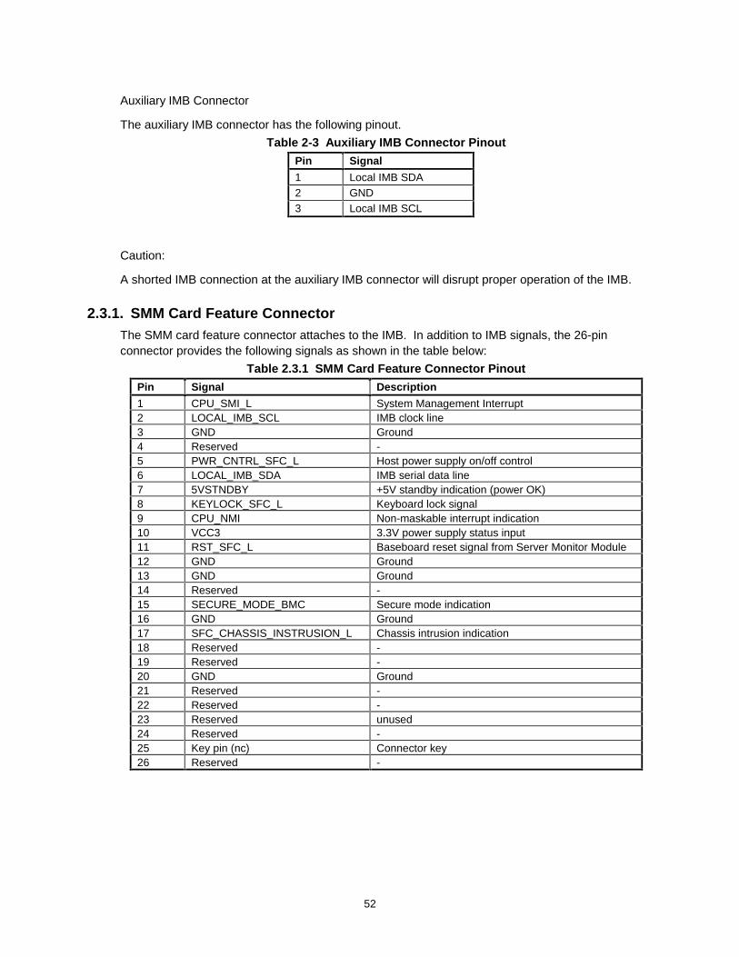
52
Auxiliary IMB Connector
The auxiliary IMB connector has the following pinout.
Table 2-3 Auxiliary IMB Connector Pinout
Pin Signal
1 Local IMB SDA 2 GND 3 Local IMB SCL
Caution:
A shorted IMB connection at the auxiliary IMB connector will disrupt proper operation of the IMB.
2.3.1. SMM Card Feature Connector The SMM card feature connector attaches to the IMB. In addition to IMB signals, the 26-pinconnector provides the following signals as shown in the table below:
Table 2.3.1 SMM Card Feature Connector Pinout
Pin Signal Description
1 CPU_SMI_L System Management Interrupt 2 LOCAL_IMB_SCL IMB clock line 3 GND Ground 4 Reserved - 5 PWR_CNTRL_SFC_L Host power supply on/off control 6 LOCAL_IMB_SDA IMB serial data line 7 5VSTNDBY +5V standby indication (power OK) 8 KEYLOCK_SFC_L Keyboard lock signal 9 CPU_NMI Non-maskable interrupt indication 10 VCC3 3.3V power supply status input 11 RST_SFC_L Baseboard reset signal from Server Monitor Module 12 GND Ground 13 GND Ground 14 Reserved - 15 SECURE_MODE_BMC Secure mode indication 16 GND Ground 17 SFC_CHASSIS_INSTRUSION_L Chassis intrusion indication 18 Reserved - 19 Reserved - 20 GND Ground 21 Reserved - 22 Reserved - 23 Reserved unused 24 Reserved - 25 Key pin (nc) Connector key 26 Reserved -

53
2.3.2. Auxiliary Power Connector A 14-pin connector is provided for power supply status indication, as well as the IMB connection. Otherpower connector pin outs are specified in the Appendix. The aux. power connector has the followingpinout:
Table 2.3.2. Auxiliary Power Connector PinoutPin Signal Pin Signal1 +5V standby power mode
sense Return2 +5V standby power mode
Sense
3 +3V Sense 4 +3V Sense Return
5 IMB Clock line 6 IMB Data line
7 GND 8 POWER_GOOD
9 PS_POWER_ON 10 GND
11 +5V standby power mode 12 nc (Key)
13 Reserved 14 VCC 24
2.4. Chassis Intrusion
The chassis intrusion header has been added to the baseboard of the N440BX Server. It is a 3-pin,shrouded and keyed connector located near the NIC indicator LEDs. Intrusion has occurred when thesignal is open, chassis is secure when pulled to ground. The chassis intrusion header has the followingpin out.
Table 2.4 Chassis Intrusion Pin-out
Pin Signal 1 Chassis Intrusion 2 GND 3 Chassis Intrusion
2.4.1. Front Panel Connector A 16-pin header is provided that attaches to the system front panel, which contains reset, NMI, and powercontrol switches, LED indicators, as well as the IMB connection. The connector has the following pinout:
Table 2.4.1. Front Panel Connector Pinout
Pin Signal Pin Signal1 GND 2 Hard disk activity LED
3 Front panel reset switch 4 Front panel power switch
5 +5V standby mode 6 nc (key)
7 Front panel NMI switch 8 POWER_COL_FP_LED_L(Power LED/blink forACPI Sleep)
9 Fan failure indicator LED 10 Chassis intrusion switch
11 Power fault LED 12 +5V standby power mode
13 IMB Data line 14 RJ45_ACTLED(LAN Active LED; supported on Astorchassis only
15 IMB Clock line 16 GND
54
2.5. Baseboard Management Controller (BMC)
On N440BX Server, all server management functionality formerly distributed between threecontrollers is concentrated in the BMC. The BMC and associated circuitry are powered from5V_Standby, which remains active when system power is switched off. The BMC is implementedusing a Dallas Semiconductor DS82CH10 micro-controller.
The primary function of the BMC is to autonomously monitor system platform management events,and log their occurrence in the non-volatile SEL. (Sensor Error Log). These events include such asover-temperature and over-voltage conditions, fan failure, or chassis intrusion. While monitoring,the BMC maintains the non-volatile SDRR (Sensor Data Record Repository), from which run-timeinformation can be retrieved. The BMC provides an ISA host interface to SDRR information, sosoftware running on the server can poll and retrieve the current status of the platform. A sharedregister interface is defined for this purpose.
SEL contents can be retrieved after system failure, for analysis by field service personnel using theSystem Setup Utility (SSU) and system management tools, such as Intel LANDesk® ServerManager. Since the BMC is powered by 5V_Standby, SEL (and SDRR) information is also availablevia the IMB. An Emergency Management Card, such as the Intel LANDesk SMM card, can obtainthe SEL and make it remotely accessible using a LAN or telephone line connection. N440BXServer introduces the Emergency Management Port (EMP), which allows remote access to the SELand other features using the COM2 port. During its watch, the BMC performs the followingfunctions:
• Baseboard temperature and voltage monitoring
• VID Bit reading
• Processor presence monitoring and FRB control
• Baseboard fan failure detection and indicator control
• SEL interface management
• SDR Repository interface management
• SDR/SEL time stamp clock
• Baseboard Field Replaceable Unit (FRU) information interface
• System management watchdog timer
• Periodic SMI timer
• Front panel NMI handling
• Event receiver
• ISA host and IMB interface management
• Secure mode control, video blank and floppy write protect monitoring and control, front panellock/unlock initiation.
• Sensor event initialization agent

55
• Wake-on LAN (WOL) via Magic Packet support
• ACPI Support
2.5.1. BMC Front Panel Control The BMC performs all front panel controller functions on N440BX Server. These include control ofsystem power, hard-resets, and the power failure LED. The BMC drives system power-on/off orhard reset from the following sources:
• Front panel push-button
• SMM card feature connector signal (controlled by secure mode)
• Transition of PIIX real-time clock alarm/suspend signal
• Command from IMB via front panel connector, aux. IMB, or SMM card
• Magic Packet signal from NIC
• Command from EMP
• Command from ISA interface
• BMC watchdog timer
2.5.2. Secure Mode The BMC monitors the SECURE_MODE signal from the baseboard keyboard controller. When thesystem is powered up, and SECURE_MODE asserted, the BMC prevents power off or reset via thefront panel power and reset push buttons. A ‘Secure Mode Violation Attempt’ event is flagged bythe BMC whenever a front panel push button is pressed. The BMC also provides options forblanking the onboard video, and write-protecting the onboard floppy interface when Secure Mode isactive.
2.5.3. Power Fault LED The BMC controls the front panel Power Fault LED signal. The BMC asserts this signal whenever itattempts to power on the system without success, and when the BMC detects a power supplyfailure. The BMC can also be directed to assert this signal via an IMB ‘Force Power Fault LED On’command.

56
2.6. Emergency Management Port (EMP)
The COM2 serial port on the N440BX Server can be configured for use as an EmergencyManagement Port (EMP). EMP provides a level of system management via RS-232 duringpowered-down, pre-boot, and post-boot situations. This allows System Management Software(SMS) interactions via point-to-point RS-232 connections, or external modem. EMP providesaccess to these basic management features:
• System power up
• System power down (Not available in restricted mode).
• System Reset (Not available in restricted mode).
• Access to the System Event Log, FRU, and Sensor Data Records.
• Access to BIOS Console Redirection.
• Password Protection
The EMP is intended for use in a secure environment. A simple password can be configured toprovide a rudimentary level of security on the interface. System configuration options can be usedto disable this interface.
The COM2 port can be used on N440BX Server for three different purposes: EMP, consoleredirection, or normal COM usage. If the BMC is using the port for EMP purposes, it is unavailableto the BIOS or SMS during this mode. If the System BIOS is using the port for console redirection,it is unavailable to the BMC or SMS (since the machine is still doing POST). Under normal usageCOM2 appears to the OS as a normal serial port; in this case the BMC and System BIOS cannotuse the port.
The N440BX Server EMP architecture supports several remote access modes, selectable using theF2 BIOS Setup Screen, as follows:
1. Pre-boot only mode - The EMP is only available while the machine is powered off and duringPOST. Just prior to booting the OS, the System BIOS disables the EMP by sending acommand to the BMC. COM2 is then available as a normal serial port.
2. SMS activated mode - Essentially the same as Pre-boot only, except that SMS software mayelect to take ownership or release control of COM2. This mode allows SMS to configure thesystem for remote access.
3. Always active mode - EMP and Console Redirect are available under the same conditions aslisted in #1 above. However, the System BIOS leaves the port enabled for run-time EMP andSMS usage. The BIOS configures the hardware such that the O/S can not “see” the port.
4. Always disabled mode - EMP and Console Redirection are not available under any conditions.
5. Restricted mode - This option can be selected in conjunction with either the ‘Pre-boot Only’ or‘Always Active’ modes listed above, using the BIOS setup interface. When activated, PowerDown control, Front Panel NMI, and Reset Control via the EMP are disabled. Power On control,System Event Log access, FRU Inventory, and Sensor Data Repository access remain enabled.Console redirection operation is unaffected by Restricted Mode.
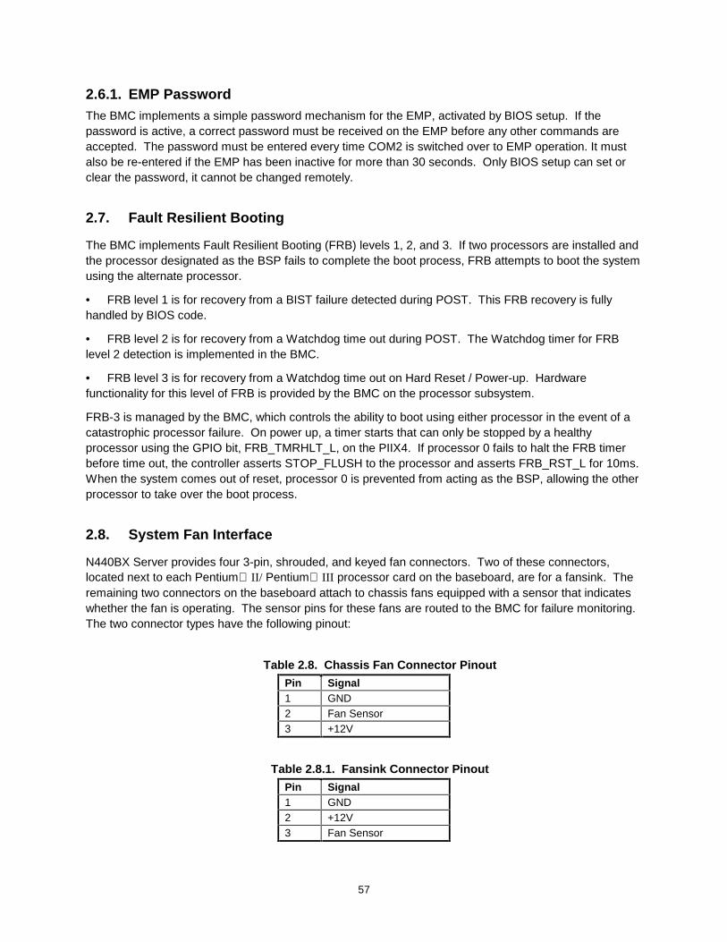
57
2.6.1. EMP PasswordThe BMC implements a simple password mechanism for the EMP, activated by BIOS setup. If thepassword is active, a correct password must be received on the EMP before any other commands areaccepted. The password must be entered every time COM2 is switched over to EMP operation. It mustalso be re-entered if the EMP has been inactive for more than 30 seconds. Only BIOS setup can set orclear the password, it cannot be changed remotely.
2.7. Fault Resilient Booting
The BMC implements Fault Resilient Booting (FRB) levels 1, 2, and 3. If two processors are installed andthe processor designated as the BSP fails to complete the boot process, FRB attempts to boot the systemusing the alternate processor.
• FRB level 1 is for recovery from a BIST failure detected during POST. This FRB recovery is fullyhandled by BIOS code.
• FRB level 2 is for recovery from a Watchdog time out during POST. The Watchdog timer for FRBlevel 2 detection is implemented in the BMC.
• FRB level 3 is for recovery from a Watchdog time out on Hard Reset / Power-up. Hardwarefunctionality for this level of FRB is provided by the BMC on the processor subsystem.
FRB-3 is managed by the BMC, which controls the ability to boot using either processor in the event of acatastrophic processor failure. On power up, a timer starts that can only be stopped by a healthyprocessor using the GPIO bit, FRB_TMRHLT_L, on the PIIX4. If processor 0 fails to halt the FRB timerbefore time out, the controller asserts STOP_FLUSH to the processor and asserts FRB_RST_L for 10ms.When the system comes out of reset, processor 0 is prevented from acting as the BSP, allowing the otherprocessor to take over the boot process.
2.8. System Fan Interface
N440BX Server provides four 3-pin, shrouded, and keyed fan connectors. Two of these connectors,located next to each Pentium II/ Pentium III processor card on the baseboard, are for a fansink. Theremaining two connectors on the baseboard attach to chassis fans equipped with a sensor that indicateswhether the fan is operating. The sensor pins for these fans are routed to the BMC for failure monitoring.The two connector types have the following pinout:
Table 2.8. Chassis Fan Connector Pinout
Pin Signal 1 GND 2 Fan Sensor 3 +12V
Table 2.8.1. Fansink Connector Pinout
Pin Signal 1 GND 2 +12V 3 Fan Sensor
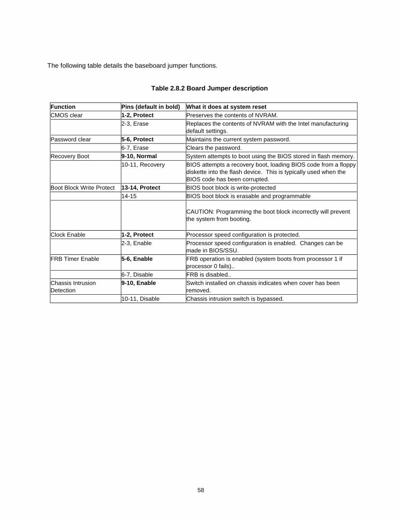
58
The following table details the baseboard jumper functions.
Table 2.8.2 Board Jumper description
Function Pins (default in bold) What it does at system reset CMOS clear 1-2, Protect Preserves the contents of NVRAM. 2-3, Erase Replaces the contents of NVRAM with the Intel manufacturing
default settings. Password clear 5-6, Protect Maintains the current system password. 6-7, Erase Clears the password. Recovery Boot 9-10, Normal System attempts to boot using the BIOS stored in flash memory. 10-11, Recovery BIOS attempts a recovery boot, loading BIOS code from a floppy
diskette into the flash device. This is typically used when theBIOS code has been corrupted.
Boot Block Write Protect 13-14, Protect BIOS boot block is write-protected 14-15 BIOS boot block is erasable and programmable
CAUTION: Programming the boot block incorrectly will preventthe system from booting.
Clock Enable 1-2, Protect Processor speed configuration is protected. 2-3, Enable Processor speed configuration is enabled. Changes can be
made in BIOS/SSU. FRB Timer Enable 5-6, Enable FRB operation is enabled (system boots from processor 1 if
processor 0 fails).. 6-7, Disable FRB is disabled.. Chassis IntrusionDetection
9-10, Enable Switch installed on chassis indicates when cover has beenremoved.
10-11, Disable Chassis intrusion switch is bypassed.
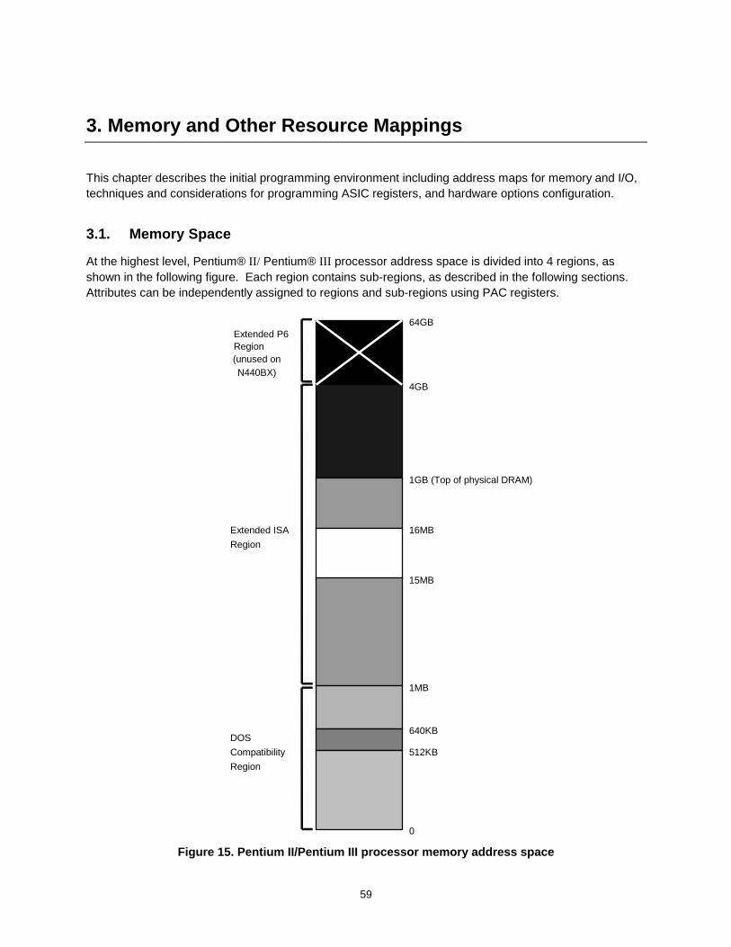
59
3. Memory and Other Resource Mappings
This chapter describes the initial programming environment including address maps for memory and I/O,techniques and considerations for programming ASIC registers, and hardware options configuration.
3.1. Memory Space
At the highest level, Pentium® II/ Pentium® III processor address space is divided into 4 regions, asshown in the following figure. Each region contains sub-regions, as described in the following sections.Attributes can be independently assigned to regions and sub-regions using PAC registers.
0
512KB
640KB
1MB
15MB
16MB
1GB (Top of physical DRAM)
4GB
64GBExtended P6Region
Extended ISA
Region
DOS
Compatibility
Region
(unused onN440BX)
Figure 15. Pentium II/Pentium III processor memory address space
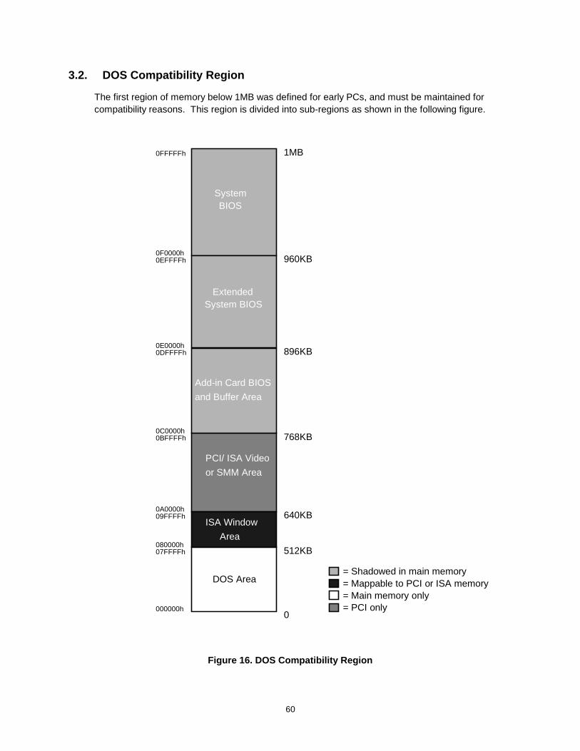
60
3.2. DOS Compatibility Region
The first region of memory below 1MB was defined for early PCs, and must be maintained forcompatibility reasons. This region is divided into sub-regions as shown in the following figure.
0
512KB
640KB
896KB
960KB
1MB
SystemBIOS
PCI/ ISA Video
or SMM Area
DOS Area
ISA Window
Area
Extended
Add-in Card BIOS
768KB
000000h
07FFFFh080000h
09FFFFh0A0000h
0BFFFFh0C0000h
and Buffer Area
0DFFFFh0E0000h
System BIOS
0EFFFFh0F0000h
0FFFFFh
= Main memory only= Mappable to PCI or ISA memory= Shadowed in main memory
= PCI only
Figure 16. DOS Compatibility Region
61
3.3. DOS Area
The DOS region is 512KB in the address range 0 to 07FFFFh. This region is fixed and all accesses go tomain memory.
3.4. ISA Window Memory
The ISA Window Memory is 128KB between the addresses of 080000h to 09FFFFh. This area can bemapped to the PCI bus or main memory.
3.5. Video or SMM Memory
The 128KB Graphics Adapter Memory region at 0A0000h to 0BFFFFh is normally mapped to the VGAcontroller on the PCI bus. This region is also the default region for SMM space. The SMM region can beremapped by programming the SMRAM Control Register in the PAC.
3.6. Add-in Card BIOS and Buffer Area
The 128KB region between addresses 0C0000h and 0DFFFFh is divided into eight segments of 16KBsegments mapped to ISA memory space, each with programmable attributes, for expansion card buffers.Historically, the 32KB region from 0C0000h to 0C7FFFh has contained the video BIOS location on a videocard. However, on N440BX Server, the video BIOS is located in the Extended BIOS or System BIOSareas.
3.7. Extended System BIOS
This 64KB region from 0E0000h to 0EFFFFh is divided into 4 blocks of 16KB each, and may be mappedwith programmable attributes to map to either main memory or to the PCI bus. Typically, this area is usedfor RAM or ROM.
3.8. System BIOS
The 64KB region from 0F0000h to 0FFFFFh is treated as a single block. By default this area is normallyRead/Write disabled with accesses forwarded to the PCI bus. Through manipulation of R/W attributes,this region can be shadowed into main memory.
3.9. Extended Memory
Extended memory on N440BX Server is defined as all address space greater than 1MB. The ExtendedMemory region covers 4GB of address space from addresses 0100000h to FFFFFFFFh, as shown in thefollowing figure.
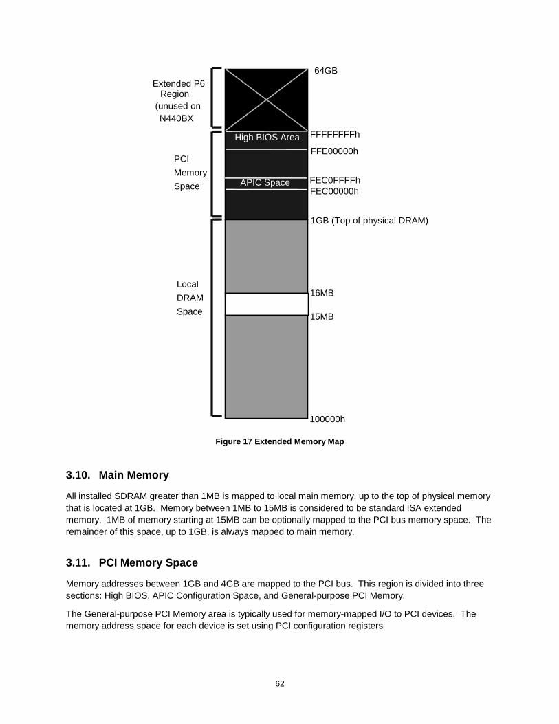
62
100000h
15MB
16MB
1GB (Top of physical DRAM)
FFFFFFFFh
64GBExtended P6
Region
DRAM
Space
(unused on
Local
Memory
Space
PCI
High BIOS Area
FFE00000h
FEC0FFFFhAPIC SpaceFEC00000h
N440BX
Figure 17 Extended Memory Map
3.10. Main Memory
All installed SDRAM greater than 1MB is mapped to local main memory, up to the top of physical memorythat is located at 1GB. Memory between 1MB to 15MB is considered to be standard ISA extendedmemory. 1MB of memory starting at 15MB can be optionally mapped to the PCI bus memory space. Theremainder of this space, up to 1GB, is always mapped to main memory.
3.11. PCI Memory Space
Memory addresses between 1GB and 4GB are mapped to the PCI bus. This region is divided into threesections: High BIOS, APIC Configuration Space, and General-purpose PCI Memory.
The General-purpose PCI Memory area is typically used for memory-mapped I/O to PCI devices. Thememory address space for each device is set using PCI configuration registers
63
3.12. High BIOS
The top 2MB of Extended Memory is reserved for the system BIOS, extended BIOS is for PCI devices,and A20 aliasing by the system BIOS. The Pentium II/Pentium III processor begins executing from theHigh BIOS region after reset. Only 256KB of the high BIOS area is actually required by the BIOS, but2MB is required by Pentium II/Pentium III processor MTRR programming.
3.13. I/O APIC Configuration Space
A 64KB block located 20MB below 4GB (0FEC00000h to 0FEC0FFFFh) is reserved for the I/O APICconfiguration space.
I/O APIC units are located beginning at a base address determined by subtracting 013FFFF0h from thereset vector. The first I/O APIC is located at FEC00000h. Each I/O APIC unit is located at FEC0x000hwhere x is the I/O APIC unit (0 through F).
3.14. Extended Pentium II/Pentium III Processor Region (above 4GB)
A Pentium II / Pentium III processor-based system can have up to 64GB of addressable memory.However, the 82440BX PCIset only supports 32-bit addressing, with the BIOS operating in 4GB ofaddress space (the memory DIMMs provide up to 512MB of main memory). All accesses to the regionfrom 4GB to 64GB are claimed by the PAC and terminated. Write data is dropped and zeroes arereturned on reads.
3.15. Memory Shadowing
Any block of memory that can be designated as read-only or write-only can be “shadowed” into memorylocated on the Pentium II/Pentium III processor bus. Typically, this is done to allow ROM code to executemore rapidly out of RAM. ROM is designated read-only during the copy process while RAM at the sameaddress is designated write-only. After copying, the RAM is designated read-only and the ROM isdesignated write-only (shadowed). Processor bus transactions are routed accordingly. Transactionsoriginating from the PCI bus or ISA masters and targeted at shadowed memory blocks will not appear onthe processor's bus.
3.16. SMM Mode Handling
A Pentium II/Pentium III processor asserts SMMEM_L in its Request Phase if it is operating in SystemManagement Mode (SMM). SM code resides in SMRAM. SMRAM can overlap with memory residing onthe Pentium II/ Pentium III processor bus or memory normally residing on the PCI bus. The PACdetermines where SMRAM space is located through the value of the SMM Range configuration spaceregister.
The SMRAM Enable bit in the SMRAM Enable configuration register will determine how the SM accessesare handled by the PAC component. When the SMRAM Enable bit is zero (SMRAM disabled), accessesto the SMM Range with SMMEM_L asserted are ignored by the PAC. When the SMRAM Enable bit isone (SMRAM enabled), accesses to the SMM range with SMMEM_L asserted are claimed by the PAC.
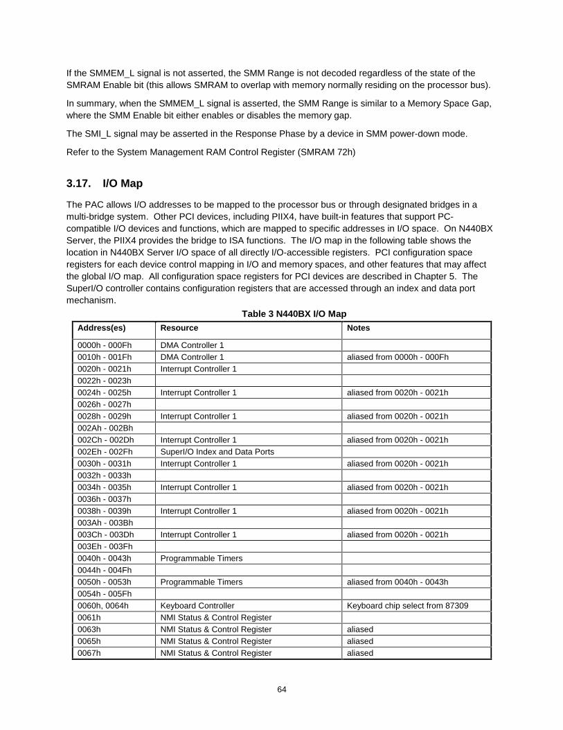
64
If the SMMEM_L signal is not asserted, the SMM Range is not decoded regardless of the state of theSMRAM Enable bit (this allows SMRAM to overlap with memory normally residing on the processor bus).
In summary, when the SMMEM_L signal is asserted, the SMM Range is similar to a Memory Space Gap,where the SMM Enable bit either enables or disables the memory gap.
The SMI_L signal may be asserted in the Response Phase by a device in SMM power-down mode.
Refer to the System Management RAM Control Register (SMRAM 72h)
3.17. I/O Map
The PAC allows I/O addresses to be mapped to the processor bus or through designated bridges in amulti-bridge system. Other PCI devices, including PIIX4, have built-in features that support PC-compatible I/O devices and functions, which are mapped to specific addresses in I/O space. On N440BXServer, the PIIX4 provides the bridge to ISA functions. The I/O map in the following table shows thelocation in N440BX Server I/O space of all directly I/O-accessible registers. PCI configuration spaceregisters for each device control mapping in I/O and memory spaces, and other features that may affectthe global I/O map. All configuration space registers for PCI devices are described in Chapter 5. TheSuperI/O controller contains configuration registers that are accessed through an index and data portmechanism.
Table 3 N440BX I/O Map
Address(es) Resource Notes
0000h - 000Fh DMA Controller 1 0010h - 001Fh DMA Controller 1 aliased from 0000h - 000Fh 0020h - 0021h Interrupt Controller 1 0022h - 0023h 0024h - 0025h Interrupt Controller 1 aliased from 0020h - 0021h 0026h - 0027h 0028h - 0029h Interrupt Controller 1 aliased from 0020h - 0021h 002Ah - 002Bh 002Ch - 002Dh Interrupt Controller 1 aliased from 0020h - 0021h 002Eh - 002Fh SuperI/O Index and Data Ports 0030h - 0031h Interrupt Controller 1 aliased from 0020h - 0021h 0032h - 0033h 0034h - 0035h Interrupt Controller 1 aliased from 0020h - 0021h 0036h - 0037h 0038h - 0039h Interrupt Controller 1 aliased from 0020h - 0021h 003Ah - 003Bh 003Ch - 003Dh Interrupt Controller 1 aliased from 0020h - 0021h 003Eh - 003Fh 0040h - 0043h Programmable Timers 0044h - 004Fh 0050h - 0053h Programmable Timers aliased from 0040h - 0043h 0054h - 005Fh 0060h, 0064h Keyboard Controller Keyboard chip select from 87309 0061h NMI Status & Control Register 0063h NMI Status & Control Register aliased 0065h NMI Status & Control Register aliased 0067h NMI Status & Control Register aliased
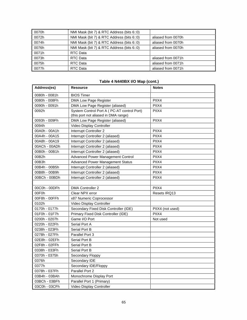
65
0070h NMI Mask (bit 7) & RTC Address (bits 6::0) 0072h NMI Mask (bit 7) & RTC Address (bits 6::0) aliased from 0070h 0074h NMI Mask (bit 7) & RTC Address (bits 6::0) aliased from 0070h 0076h NMI Mask (bit 7) & RTC Address (bits 6::0) aliased from 0070h 0071h RTC Data 0073h RTC Data aliased from 0071h 0075h RTC Data aliased from 0071h 0077h RTC Data aliased from 0071h
Table 4 N440BX I/O Map (cont.)
Address(es) Resource Notes
0080h - 0081h BIOS Timer 0080h - 008Fh DMA Low Page Register PIIX4 0090h - 0091h DMA Low Page Register (aliased) PIIX4 0092h System Control Port A ( PC-AT control Port)
(this port not aliased in DMA range) PIIX4
0093h - 009Fh DMA Low Page Register (aliased) PIIX4 0094h Video Display Controller 00A0h - 00A1h Interrupt Controller 2 PIIX4 00A4h - 00A15 Interrupt Controller 2 (aliased) PIIX4 00A8h - 00A19 Interrupt Controller 2 (aliased) PIIX4 00ACh - 00ADh Interrupt Controller 2 (aliased) PIIX4 00B0h - 00B1h Interrupt Controller 2 (aliased) PIIX4 00B2h Advanced Power Management Control PIIX4 00B3h Advanced Power Management Status PIIX4 00B4h - 00B5h Interrupt Controller 2 (aliased) PIIX4 00B8h - 00B9h Interrupt Controller 2 (aliased) PIIX4 00BCh - 00BDh Interrupt Controller 2 (aliased) PIIX4 00C0h - 00DFh DMA Controller 2 PIIX4 00F0h Clear NPX error Resets IRQ13 00F8h - 00FFh x87 Numeric Coprocessor 0102h Video Display Controller 0170h - 0177h Secondary Fixed Disk Controller (IDE) PIIX4 (not used) 01F0h - 01F7h Primary Fixed Disk Controller (IDE) PIIX4 0200h - 0207h Game I/O Port Not used 0220h - 022Fh Serial Port A 0238h - 023Fh Serial Port B 0278h - 027Fh Parallel Port 3 02E8h - 02EFh Serial Port B 02F8h - 02FFh Serial Port B 0338h - 033Fh Serial Port B 0370h - 0375h Secondary Floppy 0376h Secondary IDE 0377h Secondary IDE/Floppy 0378h - 037Fh Parallel Port 2 03B4h - 03BAh Monochrome Display Port 03BCh - 03BFh Parallel Port 1 (Primary) 03C0h - 03CFh Video Display Controller
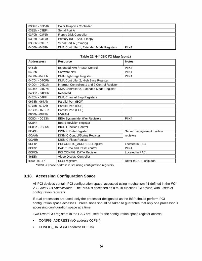
66
03D4h - 03DAh Color Graphics Controller 03E8h - 03EFh Serial Port A 03F0h - 03F5h Floppy Disk Controller 03F6h - 03F7h Primary IDE - Sec. Floppy 03F8h - 03FFh Serial Port A (Primary) 0400h - 043Fh DMA Controller 1, Extended Mode Registers. PIIX4
Table 22 N440BX I/O Map (cont.)
Address(es) Resource Notes
0461h Extended NMI / Reset Control PIIX4 0462h Software NMI PIIX4 0480h - 048Fh DMA High Page Register. PIIX4 04C0h - 04CFh DMA Controller 2, High Base Register. 04D0h - 04D1h Interrupt Controllers 1 and 2 Control Register. 04D4h - 04D7h DMA Controller 2, Extended Mode Register. 04D8h - 04DFh Reserved 04E0h - 04FFh DMA Channel Stop Registers 0678h - 067Ah Parallel Port (ECP) 0778h - 077Ah Parallel Port (ECP) 07BCh - 07BEh Parallel Port (ECP) 0800h - 08FFh NVRAM 0C80h - 0C83h EISA System Identifier Registers PIIX4 0C84h Board Revision Register 0C85h - 0C86h BIOS Function Control 0CA9h DISMIC Data Register Server management mailbox 0CAAh DISMIC Control/Status Register registers. 0CABh DISMIC Flags Register 0CF8h PCI CONFIG_ADDRESS Register Located in PAC 0CF9h PAC Turbo and Reset control PIIX4 0CFCh PCI CONFIG_DATA Register Located in PAC 46E8h Video Display Controller xx00 - xx1F* SCSI registers Refer to SCSI chip doc.
*SCSI I/O base address is set using configuration registers.
3.18. Accessing Configuration Space
All PCI devices contain PCI configuration space, accessed using mechanism #1 defined in the PCI2.1 Local Bus Specification. The PIIX4 is accessed as a multi-function PCI device, with 3 sets ofconfiguration registers.
If dual processors are used, only the processor designated as the BSP should perform PCIconfiguration space accesses. Precautions should be taken to guarantee that only one processor isaccessing configuration space at a time.
Two Dword I/O registers in the PAC are used for the configuration space register access:
• CONFIG_ADDRESS (I/O address 0CF8h)
• CONFIG_DATA (I/O address 0CFCh)
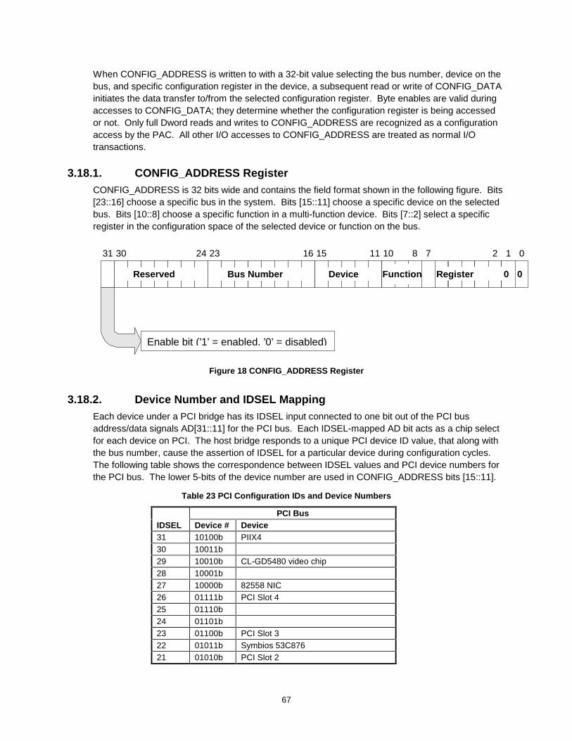
67
When CONFIG_ADDRESS is written to with a 32-bit value selecting the bus number, device on thebus, and specific configuration register in the device, a subsequent read or write of CONFIG_DATAinitiates the data transfer to/from the selected configuration register. Byte enables are valid duringaccesses to CONFIG_DATA; they determine whether the configuration register is being accessedor not. Only full Dword reads and writes to CONFIG_ADDRESS are recognized as a configurationaccess by the PAC. All other I/O accesses to CONFIG_ADDRESS are treated as normal I/Otransactions.
3.18.1. CONFIG_ADDRESS Register CONFIG_ADDRESS is 32 bits wide and contains the field format shown in the following figure. Bits[23::16] choose a specific bus in the system. Bits [15::11] choose a specific device on the selectedbus. Bits [10::8] choose a specific function in a multi-function device. Bits [7::2] select a specificregister in the configuration space of the selected device or function on the bus.
30 2
0
110 8 715 111624 2331
0
0
Reserved Bus Number FunctionDevice Register
Enable bit (’1’ = enabled, ’0’ = disabled)
Figure 18 CONFIG_ADDRESS Register
3.18.2. Device Number and IDSEL Mapping Each device under a PCI bridge has its IDSEL input connected to one bit out of the PCI busaddress/data signals AD[31::11] for the PCI bus. Each IDSEL-mapped AD bit acts as a chip selectfor each device on PCI. The host bridge responds to a unique PCI device ID value, that along withthe bus number, cause the assertion of IDSEL for a particular device during configuration cycles.The following table shows the correspondence between IDSEL values and PCI device numbers forthe PCI bus. The lower 5-bits of the device number are used in CONFIG_ADDRESS bits [15::11].
Table 23 PCI Configuration IDs and Device Numbers
PCI Bus IDSEL Device # Device 31 10100b PIIX4 30 10011b 29 10010b CL-GD5480 video chip 28 10001b 27 10000b 82558 NIC 26 01111b PCI Slot 4 25 01110b 24 01101b 23 01100b PCI Slot 3 22 01011b Symbios 53C876 21 01010b PCI Slot 2
68
20 01001b PCI Slot 1 19 01000b 18 00111b 17 00110b 16 00101b 15 00100b 14 00011b 13 00010b IDSEL Device # Device 12 00001b 11 00000b Hardwired to host bridge
3.19. Error Handling
The N440BX Server is designed to report the following types of system errors: ISA bus, PCI bus, ECCmemory, and System limit. Errors are reported using SMI_L. SMI is used for server management andadvanced error processing. All errors can be intercepted by SMI for preprocessing (if SMI_L is enabled),or handled directly by NMI handlers. Some errors have to generate an NMI even if they are intercepted bythe SMI, because the traditional way to handle errors in PC architecture is via the NMI. The N440BXemulates non-ISA errors as ISA-compatible using NMI and SMI_L.
Three error handlers are required: BIOS NMI handler, OS NMI handler, and SMI handler. The SMI hasthe highest priority to process the errors and is OS-transparent. The OS NMI handler can process allerrors as well, even when the SMI is disabled. In this case, some errors are SMI resources that can berouted to the NMI. The BIOS NMI handler processes the ISA-compatible errors and disables the NMIonly.
3.20. Hardware Initialization and Configuration
This section describes the following:
• System initialization
• Programming considerations for various portions of the I/O system
3.21. System Initialization Sequence
A Pentium II / Pentium II processor system based on the 82440BX PCIset is initialized and configuredin the following manner.
System power is applied. The power-supply provides resets using the RST_PWR_GD_BB signal. PCIreset (RST_P_RST_L) is driven to tri-state the PCI bus in order to prevent PCI output buffers from shortcircuiting when the PCI power rails are not within the specified tolerances. The PAC assertsG_CPURST_L to reset the processor(s).
The PAC is initialized, with its internal registers set to default values.
Before G_CPURST_L is deasserted, the PAC asserts BREQ0_L. Processor(s) in the system determinewhich host bus agents they are, Agent 0 or Agent 1, according whether their BREQ0_L or BREQ1_L isasserted. This determines bus arbitration priority and order.
69
The processor(s) in the system determines which processor will be the BSP by issuing BootstrapInter-Processor Interrupts (BIPI) on the APIC data bus. The non-BSP processor becomes anapplication processor and idles, waiting for a Startup Inter-Processor Interrupt (SIPI).
The BSP begins by fetching the first instruction from the reset vector.
PAC registers are updated to reflect memory configuration. SDRAM is sized and initialized.
All PCI and ISA I/O subsystems are initialized and prepared for booting.
3.22. Server Management Programming Interface
DISMIC mailbox registers provide a mechanism for communications between IMB servermanagement bus agents, and SMS or SMI handler code running on the server. DISMIC mailboxregister space, physically located in the device, is mapped to BMC external data memory and ISAI/O space. This shared register space consists of three byte-wide registers:
• Flags Register - provides semaphores for use in various defined operations
• Control/Status Register - accepts commands and returns completion codes
• Data Register - provides a port for transactions that exchange data
In addition to the ports described above, the DISMIC contains a port 070h snoop register. See thesection titled "Port 70h Snoop Register" below for further information.
SMS and SMI handler code interacts with the register interface using a variety of read and writecommands encapsulated in messages. The origin of a message is specified during a particulartransaction using Control Codes that are unique to the transaction, allowing the interface to allocatepriority to various sources, and control SMI handler and SMS precedence (the SMI handler canalways abort or temporarily interrupt any transaction).
3.22.1. Port 70h Snoop Register The Port 70h Snoop Register reads back the state of bit 7 of I/O port 70h (RTC NMI enable bit) tothe BMC. This register shadows any ISA write to port 70h. Due to architectural constraints in theDISMIC, the contents of this register cannot be made available for direct I/O read access at analternate address location on the ISA bus. Access to the register’s contents is provided onlythrough the BMC using a command defined for this purpose.
3.23. PCI Interrupt to IRQ Routing Control
Embedded in a separate programmable logic device is logic for rerouting of PCI interrupts to ISAIRQs. Two I/O locations are reserved by the BIOS using the PIIX4 Programmable Chip SelectControl register, for control of the PCI to IRQ re-router feature: CA4h and CA5h. Writes to theupper and lower nibble of each byte determine whether the interrupt is passed through to the I/OAPIC, or rerouted to an ISA IRQ input on the PIIX4. The following figure shows the PCI interruptline associated with each nibble. The following table defines the encoding of each nibble.
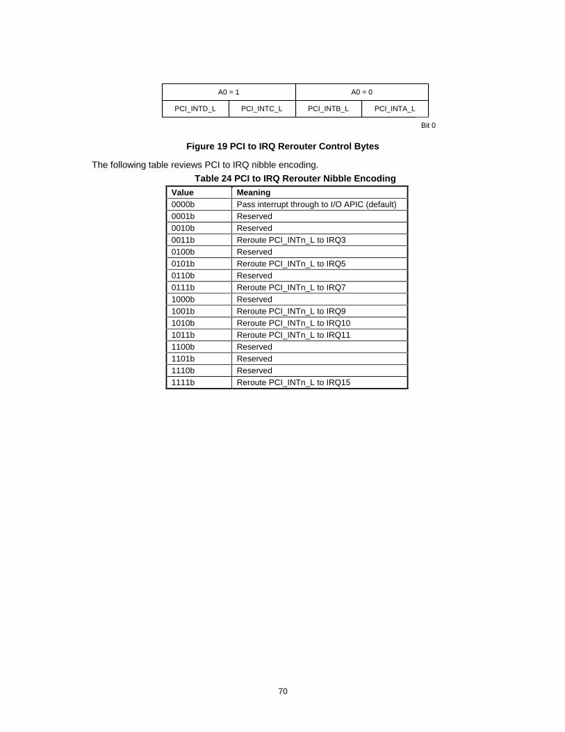
70
A0 = 1 A0 = 0
PCI_INTD_L PCI_INTA_LPCI_INTB_LPCI_INTC_L
Bit 0
Figure 19 PCI to IRQ Rerouter Control Bytes
The following table reviews PCI to IRQ nibble encoding.
Table 24 PCI to IRQ Rerouter Nibble Encoding
Value Meaning 0000b Pass interrupt through to I/O APIC (default) 0001b Reserved 0010b Reserved 0011b Reroute PCI_INTn_L to IRQ3 0100b Reserved 0101b Reroute PCI_INTn_L to IRQ5 0110b Reserved 0111b Reroute PCI_INTn_L to IRQ7 1000b Reserved 1001b Reroute PCI_INTn_L to IRQ9 1010b Reroute PCI_INTn_L to IRQ10 1011b Reroute PCI_INTn_L to IRQ11 1100b Reserved 1101b Reserved 1110b Reserved 1111b Reroute PCI_INTn_L to IRQ15
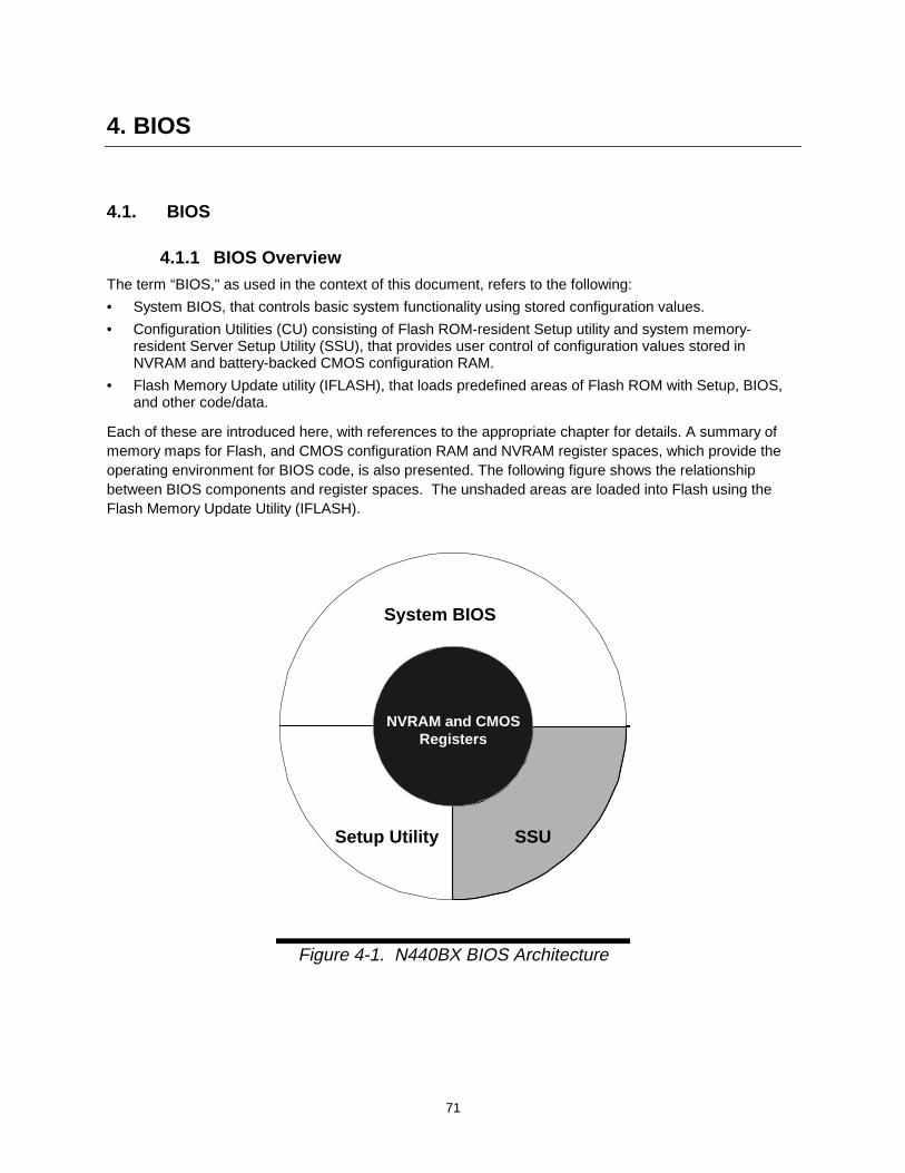
71
4. BIOS
4.1. BIOS
4.1.1 BIOS OverviewThe term “BIOS," as used in the context of this document, refers to the following:
• System BIOS, that controls basic system functionality using stored configuration values.
• Configuration Utilities (CU) consisting of Flash ROM-resident Setup utility and system memory-resident Server Setup Utility (SSU), that provides user control of configuration values stored inNVRAM and battery-backed CMOS configuration RAM.
• Flash Memory Update utility (IFLASH), that loads predefined areas of Flash ROM with Setup, BIOS,and other code/data.
Each of these are introduced here, with references to the appropriate chapter for details. A summary ofmemory maps for Flash, and CMOS configuration RAM and NVRAM register spaces, which provide theoperating environment for BIOS code, is also presented. The following figure shows the relationshipbetween BIOS components and register spaces. The unshaded areas are loaded into Flash using theFlash Memory Update Utility (IFLASH).
System BIOS
Setup Utility SSU
NVRAM and CMOSRegisters
Figure 4-1. N440BX BIOS Architecture
72
4.1.1. System BIOS over viewThe system BIOS is the core of the Flash ROM-resident portion of the BIOS. The system BIOS providesstandard PC-BIOS services and some new industry standards, such as I2O, Plug and Play, DMI andACPI. In addition, the system BIOS provides support for these N440BX specific features: securityfeatures, multiple-speed processor support, SMP support, fault resilient booting (FRB), logging of criticalevents, server management features, CMOS configuration RAM defaults, multiple language support,defective DIMM detection and remapping, automatic detection of video adapters, PCI BIOS interface,option ROM shadowing, system information reporting, ECC support, SMI support, user-supplied BIOSsupport, L2 cache support, memory sizing, boot drive sequencing, and resource allocation support.
4.1.2. Configuration UtilitiesThe SSU provides the means to configure on board hardware devices and add-in cards. The SSUconsists of the following:
• Standard PC-AT Setup utility, embedded in Flash ROM, for configuration of on board resources.
• SSU, for configuration of add-in cards as well as on board resources, which must be run from a bootdiskette or CD-ROM shipped with the system.
4.1.3. Flash Update UtilityThe system BIOS and the setup utility is resident in partitioned Flash ROM. The device is in-circuit re-programmable, except for the recovery boot block, which is electrically protected from erasure. A jumperon the baseboard can enable writing to boot block.
To reload Flash memory from a floppy disk (or from CD-ROM), use a Flash update utility. The file to beloaded contains a new copy of BIOS code. The utility must match the board ID with the one in the load fileto protect against reprogramming the Flash with BIOS for another platform. Baseboard revisions mayshare a common SSU but may require different BIOS code.
4.1.3.1. System Flash ROM layout
The Flash ROM contains system initialization routines, Setup utility, and runtime support routines. Theexact layout is subject to change, as determined by Intel. All areas are 64KB in size (symmetric flash).64KB is reserved for diagnostic boot loader and an 8KB User block is available for user ROM code orcustom logos. 64KB area is used to store the string database. The complete ROM is visible, starting atphysical address 4GB less 512KB. The Flash Memory Update utility loads BIOS components to blocks ofspecified length and location, as summarized in Table 4-1: Flash Map Summary. This is a typical exampleof a Flash block table.

73
Table 4-1. Flash ROM Map Summary
Length Base Address Usage
1000h 0FFF80000h ESCD (4k) see below9000h 0FFF81000h DMI , SCSI NVRAM, Multiboot data10000h 0FFF90000h Console Redirection2000h 0FFF98000h User Binary4000h 0FFF9C000h Diagnostic Boot Area10000h 0FFFA0000h BIOS block10000h 0FFFB0000h BIOS block (smm handler)10000h 0FFFC0000h BIOS block (strings, SCSI BIOS)10000h 0FFFD0000h BIOS block (video BIOS, setup)C000h 0FFFE0000h BIOS block4000h 0FFFEC000h Recovery Block10000h 0FFFF0000h BIOS block
None of the above blocks are visible at the aliased addresses below 1 MB due to shadowing. The abovetable is representative only of the information contained in the Flash ROM. The BIOS alone needs to knowthe exact map. Intel reserves the right to change the Flash map without notice. All block in this flash partare 64k (10000h) in length. The BIOS will adjust the size of each component to fit in a given block. Onlythe Recovery block, ESCD and DMI are fixed at a given location.
Offset Length Description0 1000h Plug-n-Play ESCD1000h 0180h DMI information1180h 0080h Mfg.1200h 0100h Custom CMOS1300h 0200h Multiboot1500h 0020h Hard Drive1520h 0080h SCSI B1700h 01F4h Scratch18f4h 070ch SCSI A2000h 2810h Processor Patch BIOS Update4810h 0040h System ID4850h 0020h OEM Throttle Register
74
4.2. System BIOS
This chapter describes those features of the system BIOS that are unique to N440BX. The N440BXplatform does not provide legacy support USB. Legacy mode of USB keyboard emulating a PS/2 keyboardvia SMM is not supported on N440BX. While devices such as USB keyboards will work with OS drivers,these keyboards will not respond during BIOS POST. The following groups of system BIOS features aredescribed here:
• Security features
• Auto-configuration features
• Performance features
• Reliability features
• System services
• OEM customization hooks
• Console redirection
• I2O support
• DMI support
• POST Memory Manager Support
• ACPI support
4.3. Security Features
The BIOS provides a number of security features. This section describes the security features andoperating model.
4.3.1. Operating ModelThe following table summarizes the operation of security features supported by the BIOS.
Table 4-2. Security Features Operating Model
Mode Entry Method/Event
EntryCriteria
Behavior ExitCriteria
After Exit
Securemode
KeyboardInactivity Timer,Runtime activationof KBC Hotkey
UserPasswordenabled inSSU
• Screen goes blank (ifenabled in SSU).
• Floppy writes aredisabled (if selected inSSU).
• Power and Resetswitches on the frontpanel are disabled(ifenabled in Setup).
• No mouse or keyboardinput is accepted.
UserPassword
• Video isrestored.
• Floppy writes areenabled.
• Power and Resetswitches areenabled.
• Keyboard andmouse inputs areaccepted.
75
Table 4-3. Security Features Operating Model
Mode Entry Method/Event
EntryCriteria
Behavior ExitCriteria
After Exit
Secure boot Power On/Reset UserPasswordandSecure BootEnabled inSSU
• Enter secure mode.• Prompts for Password, if
booting from drive A.• Video is blanked (if
enabled in Setup).• Floppy writes are
disabled (if programmedin SSU ).
• Power and Resetswitches on the frontpanel are disabled(ifprogrammed in SSU ).
• No mouse or keyboardinput is accepted;however, the Mousedriver will be allowed toload before a passwordis required.
• If booting from drive A,and the user enterscorrect password, thesystem boots normally.
UserPassword
• Floppy writes areenabled.
• Power and Resetswitches areenabled.
• Keyboard andmouse inputs areaccepted.
• System attemptsto boot from driveA. If the userenters correctpassword, anddrive A isbootable, thesystem bootsnormally
Password onboot UserPasswordboot (ATstyle)
Power On/Reset UserPasswordset andpassword onbootenabledandSecure BootDisabled inSSU
• System halts for UserPassword before booting.The system is not insecure mode.
• Video is blanked (ifenabled in SSU ).
• Floppy writes aredisabled (if programmedso by SSU ).
• No mouse or keyboardinput is accepted.
UserPassword
• Keyboard andmouse inputs areaccepted.
• The systemboots normally.Boot sequence isdetermined bySSUoptions.
DisketteAccess
Power On/Reset Set featureto Admin inSSU
User is prevented fromaccessing the floppy drive.Administrator is alwaysprevented from accessing thefloppy drive.
Setfeature toUser inSSU
User is allowed toaccess the floppydrive.
Fixed diskboot sector
Power On/Reset Set featureto WriteProtect inSSU
Will write protect the bootsector of the hard drive toprevent viruses fromcorrupting the drive.
Setfeature toNormal inSSU
Hard drive willbehave normally.
4.3.2. Password ProtectionThrough the use of passwords, the BIOS prevents unauthorized tampering with the system. Once securemode is enacted, access to the system is allowed only after you have entered the correct password(s).Each of two passwords, for User and Administrator, can be created during system configuration using theSSU .
Once secure mode is enacted, access to the system is allowed only after you have entered the correctpassword. Each password, User and Administrator, can be created during system configuration using theSSU . Once set, a password can be disabled by changing it to a null string. The Administrator password
76
can still modify the time and date, but other fields can only be modified if the user password is entered.For example, system hardware configuration can be controlled by the User password, while Administratorcontrol access to the machine’s file system. If only an administrator password is set (no User password),this password is requested when entering Setup and must be entered before the majority of the fields canbe modified. If only the User password is set (no administrator password), the User password must beentered to access Setup, but all fields can be modified once entered.
Once set, a password can be disabled by changing it to a null string.
4.3.2.1. Inactivity timer
If the inactivity timer function is enabled, and no keyboard or mouse actions have occurred for thespecified time-out period, the following occurs until the User password is entered:
• Keyboard and mouse input is disabled
• Video is blanked (if programmed in SSU )
• Floppy drive is write protected (if enabled)
• Front panel reset and power switches are locked (if enabled)
• A time-out period may be specified with the SSU .
4.3.2.2. Hot key activation
A Hotkey combination can activate secure mode immediately, rather than having to wait for the inactivitytime-out to expire. The Hotkey combination is set using the SSU . The following keys are valid hot keys :A-Z, 0-9.
4.3.2.3. Password clear switch
The BIOS determines if the password clear jumper is set. If set, any passwords are cleared from CMOSand password protection is disabled.
4.3.3. Floppy Write ProtectionIf enabled by the SSU , floppy disk writes are blocked when the system is in secure mode. Floppy writeprotection is only in effect while the system is in secure mode. Otherwise, write protection is disabled.
4.3.4. Power Switch and Reset Button LockIf enabled by the SSU , the power switch and reset button are disabled when in secure mode.
4.3.5. Secure Boot (Unattended Start)Secure Boot allows the system to boot and run the OS. However, until the User password is entered,mouse and keyboard input is not accepted and the front panel reset/power switches are disabled. TheSSUis used to place the system into secure boot mode. In secure boot mode, if the BIOS detects a floppydisk in the A drive at boot time, it prompts the User for a password. When the password is entered, thesystem can boot from the floppy and secure mode is disabled. Any one of the secure mode triggers causethe system to go back into secure mode. If there is no disk in drive A, the system boots from the next bootdevice and is placed in secure mode automatically. All of the enabled secure mode features go into effectat boot time.
77
4.3.6. Interaction with External UtilitiesExternal utilities that need to perform password validation, such as SSU, can call the appropriate BIOSinterface. The BIOS performs the password validation and returns the status. The interface is notdescribed here for security reasons.
4.4. Auto-Configuration Features
The BIOS provides support for auto-configuration of the following:
• Plug and Play
• Processor speed
• SMP initialization
• Memory sizing
• Boot drive selection
• Mouse and keyboard swapping
• Pentium® II/ Pentium® III processor BIOS update
• LCD support
4.4.1. Plug and PlayThe BIOS supports the following industry standards for full Plug and Play capabilities:
• Plug and Play (PnP) ISA specification
• Desktop Management Interface (DMI) BIOS specification
• Extended System Configuration Data Specification (EISA is not supported).
• PCI local Bus specification
4.4.1.1. Resource allocation
The system BIOS identifies, allocates, and initializes resources in a manner consistent with other Intelservers. The BIOS scans for the following, in order:
1. ISA devices: If an ISA device is found, it is initialized and given resource priority over other devicesof the same type plugged into the system.
2. Off board PCI devices: If found, the BIOS initializes and allocates resources to these devices.
3. On board Video, IDE, and SCSI devices: If equivalent functionality is not found off board, the BIOSallocates resources according to the parameters set up by the SSU.
4.4.1.2. PnP ISA auto-configuration
The BIOS:
• Fully supports the PnP ISA protocol
• Reads the PnP ISA configuration port
• Assigns the system I/O, memory, DMA channels, and IRQs from the resource pool
· The Super I/O* chip is an example of a PnP ISA device.
4.4.1.3. PCI auto-configuration
The BIOS supports the INT 1Ah, AH = B1h functions, in conformance with the PCI specification, Rev. 2.1.BIOS also supports the 16 and 32-bit protected mode interfaces as required by the PCI BIOSspecification. System POST performs auto-detection and auto-configuration of ISA, ISA Plug-N-Play, and
78
PCI devices. This process maps each device into memory and/or I/O space, and assigns IRQs and DMAchannels as required, so that there are no conflicts prior to booting the system. BIOS scans the PCIdevices on each PCI bus in low to high sequence. The PCI busses are also scanned in the same order.The BIOS programs the PCI-ISA interrupt routing logic in MISSMIC to steer PCI interrupts to compatibleISA IRQs.
The BIOS detects the presence of I2O compliant intelligent controllers, such as i960 RD and configuresthem as documented in the I2O BIOS specification. The BIOS queries each I2O IOP to find out if a PCIdevice is controlled by IOP and does not enable the devices under IOP control and does not allocate IRQresources to such devices.
Drivers and OS programs can determine the installed devices and their assigned resources using theBIOS interface functions. The BIOS does not support devices behind PCI-to-PCI bridges that requiremapping to the first 1 MB of memory space due to architectural limitation. (Refer to PCI-to-PCIArchitecture Specifications). The User can override the IRQ assigned to a PCI card by using SSU.
4.4.1.4. Legacy ISA configuration
Unlike Plug-N-Play cards, legacy ISA cards do not provide any mechanism by which the BIOS can find outtheir resource requirements. Further, legacy ISA cards cannot be configured and require fixed resources.The SSU utility helps the user configure the Legacy ISA devices. The SSU utility allows the end user toreserve the Legacy ISA system resource and save the information into NVRAM. The POST resourcemanagement will not allocate the resources that are reserved for legacy ISA cards to PnP devices.
4.4.1.5. On board device auto-configuration
The BIOS detects all on board devices and assigns appropriate resources. The BIOS dispatches theoption ROM code for the on board devices to DOS compatibility hole (C0000h to E7FFFh) and transferscontrol to the entry point. User may disable scanning of the on-board Symbios SCSI ROM using the SSU .
4.4.1.6. Automatic detection of video adapters
The BIOS looks for video adapters in the following order:
1. ISA
2. PCI
3. Baseboard
The on board (or off board) video BIOS is shadowed, starting at address C0000h, and is initialized beforememory tests begin in POST. Precedence is always given to off board devices.
4.4.2. Multiple Processor SupportThe BIOS supports one or two Pentium® II/ Pentium® III processors. The processors and IO APIC IRQrouting are described in a table specified in the next section. If only one processor is installed the otherslot must be populated with a terminator. In a single processor system the APIC table and ACPI tables aredynamically updated to reflect the actual status of good processors in the system.
4.4.2.1. Multiprocessor specification support
The BIOS complies with all requirements of the Intel Multi-Processor Specification (MPS) version 1.4 forSymmetric Multi-Processor (SMP) support, as well as MPS version 1.1, for backward compatibility. Theversion number can be configured using the SSU . The base MP Configuration Table contains thefollowing entries:
79
• MP table header
• Processor entries
• PCI bus entries
• I/O APIC entries
• I/O interrupt entries
• Local interrupt entries
The extended MP table is constructed if MPS version 1.4 is selected. It contains these entries:
• System address space mapping entries
• Bus hierarchy descriptor
• Compatibility bus address space modifier entries
· Note: The MP APIC table and ACPI table are the only places where the number of processors aredynamically reported from boot to boot.
4.4.2.2. Multiple processor support
On reset, the Primary Processor is selected by the BMC to become the BootStrap Processor (BSP). Theslot labeled Primary CPU will always be examined first. If a serious error is detected during Built-In SelfTests (BIST), that processor does not participate in the initialization protocol and the Secondary processorthen becomes the BSP and the Primary is halted and removed from the MP table. Whichever processorsuccessfully passes BIST is automatically selected by the hardware as the BSP and starts executing fromthe reset vector (F000:FFF0h). A processor that does not perform the role of BSP is referred to as anApplication Processor (AP).
The BSP is responsible for executing POST and preparing the machine to boot the OS. BIOS performsseveral other tasks in addition to those required for MPS support. These tasks are part of the faultresilient booting algorithm. At the time of booting, the system is in virtual wire mode and the BSP alone isprogrammed to accept local interrupts (INTR driven by the PIC and NMI). As a part of the boot process,the BSP wakes up the APs. When woken up, the AP programs its memory type range registers (MTRRs)so that they are identical to those of the BSP. All APs execute a halt instruction with their local interruptsdisabled.
4.4.2.3. Multiple Processor speed support
The BIOS supports different steppings of Pentium® II/Pentium® III processors as long as they are within 1release of each other. Both processors must be of the same cache size. Two processor modules ofdifferent operating frequency are allowed within a single system configuration however the system will onlyoperate reliably at the slower of the two. All installed processors must run at the same frequency (forexample, the bus and core frequencies of all processors must be identical). Also, for best performance, allprocessors must be of the same CPU ID.
The type and speed of all detected processors are also reported by the SSU .
4.4.3. Memory SizingDuring POST the BIOS:
• Tests and sizes memory
• Configures the memory controller
80
Nightshade supports various size and configurations of ECC SDRAM DIMMS. Memory sizing andconfiguration are only guaranteed for qualified DIMMs approved by Intel. The BIOS gathers all type, size,speed and memory attributes from the on-board EEPROM or SPD on the memory DIMM. It is requiredthat the memory be stuffed from the lowest DIMM socket to the highest for the memory to work in allconfigurations over the full environmental range of the server.
The memory sizing algorithm determines the size of each row of DIMMs. The BIOS reads the DIMMspeed information and programs the PAC accordingly. BIOS does not perform the extended memory testif instructed by the user via SSU . Disabling the extended memory test reduces the boot time. In any case,the BIOS always initializes ECC memory. The BIOS is capable of detecting, sizing, and testing anyamount of RAM, up to the physical maximum of 1 GB. The BIOS is capable of reporting up to 64 MBusing INT 15h, AH = 88h, or INT 15h, function E801h, which can report up to 4,096 MB. INT 15h, functionE820h supports reporting of the system memory regions.
4.4.4. Boot Device SelectionThe BIOS conforms to the Phoenix BIOS boot specification 1.01. The BIOS boot specification describes amethod where the BIOS identifies all Initial Program Load (IPL) devices in the system, prioritizes them inthe order the user selects, and then sequentially goes through each device and attempts to boot. It ispossible to use the SSUto change the boot order of devices connected to the system. In the case wherethe order has been changed by a user, the system boots in the order chosen, with the exception of legacydevices. Legacy devices are those devices that tend to take control of the boot process altogether byhooking boot vector (interrupt 19h). Further, they provide no means for identifying themselves as an IPLdevice. Therefore, the BIOS cannot selectively boot from one of several Legacy IPL devices in a system.The user can choose whether the first boot device is a floppy, a CDROM, a hard drive, an I2O devicethrough SSU . The system BIOS will try and boot from devices in the order specified by the user. Further,the user can reorder the hard drives and choose the C: drive to be any IDE drive or any drive that iscontrolled by a Boot BIOS Specification compliant option ROM BIOS, such as the on-board SymbiosBIOS. Hard drives that are controlled by all other controllers will appear as ‘Other bootable cards” in thesetup menu, and the user cannot control the order on drive by drive basis for such controllers. Some bootBIOS compliant option ROM BIOS’s may present all the drives as a single device, and may not allow theuser to manipulate the order on a drive by drive basis. The user is responsible for making sure that the C:drive has a bootable image, if booting from a hard drive.
4.4.5. Mouse and Keyboard SwappingThe BIOS allows users to swap the keyboard and PS/2 mouse connectors before system the is poweredon. It detects the combination during POST and initializes the KBC accordingly. Hot plugging of the mouseand keyboard is not supported by Nightshade and may have unpredictable results.
4.4.6. Pentium® II/Pentium® III Processor BIOS Update APIThe Pentium® II/Pentium® III processor has the capability to correct specific errata through the loading ofan Intel supplied data block. The Pentium Pro processor BIOS update specification defines a way ofincorporating future releases of such data block (also called the “update”) into a system BIOS. The BIOSis responsible for storing the update in a non-volatile memory block and loading it into each Pentium II/Pentium III processor during POST sequence. The Pentium Pro processor BIOS update specificationrequires the system BIOS to implement function calls to read the update and overwrite the existing updatewith a new release. These functions can be accessed from real mode by executing INT 15 withAX=0xD042. The corresponding 16-bit protected mode interface is not implemented. BIOS performs allthe recommended security checks before validating an update.
81
4.4.7. Boot Without KeyboardThe system can boot with or without a keyboard. There is no entry in the SSU for keyboardenable/disable. The presence of the keyboard is detected automatically during POST, and the keyboard istested if present. The BIOS will not detect or use USB keyboards.
4.5. Performance Features
For enhanced performance, the BIOS sets up the L2 cache controller for the Pentium® II/ Pentium® IIIprocessor and performs option ROM shadowing.
4.5.1. L2 cache initializationThere are differences between the Pentium® II/Pentium® III processor cache implementation andprevious Intel processor architectures. To boost system performance, the Pentium II/Pentium IIIprocessor contains an L2 cache and cache controller; which previously had been handled by externaldevices. BIOS programs L2 cache controllers of each processor in a manner that is consistent with theother processor and the PCIset.
L2 cache is tested as a part of the Pentium II/Pentium III processor BIST. If L2 cache is bad, the PentiumII/ Pentium III processor indicates the error in the BIST and the BIOS disables the Processor. The BIOSdetects the cache size and cache type (ECC or non-ECC), and programs the cache controller accordinglybefore performing any cache operations. The BIOS displays a warning message on the screen if the twoprocessors have different cache sizes. Not all bus to core ratio settings support L2 cache being on.Some bus to core ratios are not allowed by the processor and the BIOS will disable the cache accordinglywith the registers in the processor.
4.5.1.1. Cache state on boot
The BIOS looks at a bit in CMOS to determine if the system caches should be enabled or disabled. Theuser can modify the bit in the Boot Options of the Setup Main menu. If the cache is enabled, cachecontrollers in all Pentium II/ Pentium III processors are initialized in a consistent manner with each otherand the 82440BX PCI Set.
4.5.2. Option ROM ShadowingAll on board adapter ROMs (stored in compressed form in the system Flash ROM), and PCI adapterROMs are shadowed into RAM in the ISA-compatible ROM adapter memory space between C0000h toE7FFFh. The BIOS ROM found on ISA devices are shadowed (if capable) into adapter memory space inthe same range after initialization. Shadowing for ISA devices can be disabled for various regions usingthe SSU . PCI BIOS ROMs are always shadowed. Typically the onboard video bios is shadowed atC0000h.
4.5.3. Memory speed optimizationThe BIOS detects the system memory speed and bus speed and optimizes the memory controller for thebest performance.
The system bus speed can be detected by the processor internal speed and the bus ratio. The memoryDIMM speed can be detected by its ID. Using this information the BIOS can set up the memory controllerregister for the best performance.

82
4.5.4. PCIset performance optimizationThe BIOS detects the system configuration, such as board ID, PCIset stepping, processor stepping, andoptimizes the PCIset for the best performance. Most of the PCIset registers are automatically. The biosno longer supports 1 Megabyte holes at 15-16 Megabyte memory regions. The user may be allowed tocontrol a limited number of performance features. It is not recommended for the user to change any ofthe default PCI timing settings.
83
4.6. Reliability Features
The BIOS supports several features to create a robust computing environment including the following:
• ECC memory and defective DIMM handling
• Fault resilient booting
• Logging of critical events
• I2C system management bus
• CMOS default override
• Emergency Management port
4.6.1. Defective DIMM detection and remappingThe ECC memory subsystem on N440BX is able to detect single-bit errors (SBE) and certain multi-biterrors (MBE) during reads from and writes to system DRAM. Single-bit errors can be detected andcorrected. Certain patterns of MBEs can be detected but cannot be corrected, whereas other types ofMBEs cannot be detected.
During POST memory testing, detection of single-bit and multi-bit errors in DRAM banks is enabled. Anyerror is avoided by reducing the usable memory in that bank so that the byte containing the hard error isno longer accessible. This is done automatically by the BIOS during POST and does not require any userintervention. The BIOS logs the errors in the nonvolatile system event log. The BIOS detects the speed ofindividual DIMMs. The BIOS disables a DIMM that is slower than what the hardware requires and displaysa warning message.
4.6.1.1. Memory configuration algorithm
The algorithm for determining memory configuration is as follows:
If there is no DIMM population, or the DIMMs are all bad, or have the wrong speed, the BIOS sounds abeep code error and POST is terminated. The BIOS requires at least 4 MB of good memory for POST tostart up. The BIOS individually probes each bank for the size of installed DIMMs. The BIOS detects thespeed and type of the DIMM SDRAM and programs the PCIset accordingly. If the bank does not matchone of the allowable configurations, the BIOS reports the error with an error message. EDO memory isnot physically supported due to the memory socket used on the baseboard. Non ECC memory will besupported but not tested or validated by Intel. The BIOS will automatically shut off all ECC capability forthe system if detected. All configuration data for the memory DIMMs is gathered by the BIOS from theSPD or EEPROM on the DIMM. This is done via the SMBUS interface on the PIIX4.
In the event that the BIOS disables or resizes a bank, an error message displays with the DIMM numberof the failing memory. Another message informs the user that the amount of usable memory in that bankis being reduced to eliminate the failing location. Eliminating hard errors in this way during POST is doneas a precaution to prevent an SBE from becoming an MBE after the system has booted and to preventSBEs from being detected and logged each time the failed location(s) are accessed. This is recorded inthe SEL (System Event Log) at both post time as well as runtime with an SMI. See the Servermanagement specification for the format of the memory errors in the SEL. This is implemented as anEEPROM that the BMC can access directly with the server on or off.
If the error is an SBE, the 440BX automatically corrects the data before it is returned to memory. The440BX memory controller scrubs the memory location where the error occurred to correct the SBE and
84
the BIOS will record the SBE via an SMI to the SEL. If the error is an MBE, this condition is consideredfatal, and after the error is logged, an NMI is generated, telling the OS to handle this fatal error.
4.6.1.2. ECC Memory Initialization
The system BIOS handles ECC memory initialization. All memory locations, including SystemManagement RAM and shadow memory region, are unconditionally initialized during POST (set to 0).Error detection is disabled while ECC memory is initialized to prevent false alarms caused by un-initialized memory bytes. If hard errors are detected during the memory test, the memory partitioncontaining the errors is resized to eliminate the failing locations.
4.6.1.3. ECC and SMI support
During normal operation, any SBEs (single bit errors) are detected and are handled by the SMI supportcode. The SMI code logs the SBE, keeping up to 3 records of the last SBE logs in the system event log.The 440BX memory controller cannot locate the exact address of the error, but can only point to the rowthat contains the error location. Scrubbing is always automatically enabled when ECC memory isdetected. The row containing the failing location is scrubbed by reading the corrected data and writingback the correct data automatically by the memory controller. If read from shadow memory results in anSBE, the BIOS must enable writes to that area, scrub the locations and disable writes. Scrubbing helps toprevent a single-bit correctable error from turning into multiple-bit errors in the future. Scrubbing an entirerow is a time consuming operation and might affect correct functioning of certain operating systems. IfMBEs are detected, the BIOS SMI handler will log an event into the SEL (System Event Log) and thengenerate an NMI to the OS. This is part of the server management control functions which the BMCprovides with its non-volatile storage device (available out of band).
The ECC memory feature may be disabled if significant performance increase is measured in thePlatform. The BIOS setup will provide a switch to disable ECC memory. The default will be for ECC to beenabled. This switch will disappear in the shipping release if the performance is not deemed significant.
4.6.2. Fault Resilient Booting (FRB)The BIOS and firmware provides a feature to guarantee that the system will boot even if one processorfails during POST or hangs while booting to the O/S. The BMC contains 2 watchdog timers that if they tripwill reset the system. The first timer(FRB-3) starts counting down whenever the system comes out of hardreset and usually is about 5 seconds. If the BSP successfully resets and starts executing the BIOS willdisable the FRB-3 timer in the BMC and system will continue on with POST. If the timer expires becauseof the BSP’s failure to fetch or execute BIOS code, the BMC resets the system and disables the failedprocessor. The system will continue to reset alternating BSP’s between the primary and secondaryprocessor socket until the BIOS POST gets past disabling the FRB-3 timer in the BMC.
The second watchdog timer(FRB-2) in the BMC is set to 5-6 minutes and is designed to guarantee thatthe system will complete BIOS POST. Near the end of POST, before the options ROMs are initialized, theBIOS will disable the FRB-2 timer in the BMC. If the system hangs during POST, the BIOS will fail todisable the timer in the BMC which generates an ASR (Asynchronous System Reset).
In a dual processor system the BIOS will register the AP in the MP table. When started by the BSP, if anAP fails to complete initialization within a certain time, it is assumed to be non-functional. This AP is notlisted in the MP table (refer to the MP Specifications, Rev. 1.4) and is invisible to the OS. If eitherprocessor fails the BIST (Built-In Self Test) it is marked bad and removed from the MP table. The BIOSwill disable the processor and reset the system to make sure the failed processor will be electricallydisabled on the next boot.
85
The BMC maintains a flag bit in non-volatile ROM for each processor. This bit is used to store aprocessor’s track record. It is set whenever a processor fails and remains so until the user forces thesystem to retest the processor and it successfully makes it past both FRB timers. The BIOS reminds theuser about a previous processor failure during each boot cycle and keeps that processor disabled until thestatus flag is cleared by the user. Processors that have failed in the past are not allowed to become theBSP3, and are not listed in the MP table. It might happen that all the processors in the system are markedbad. An example is a uniprocessor system where the processor has failed in the past. If all the processorsare bad, the BIOS does not alter the BSP and attempts to boot from the original BSP. It also informs theuser that it is trying to boot from a failed processor if the POST gets executed. Error messages aredisplayed on the console, errors are logged in the event log if a processor fails. The failed processor isidentified by its number.
If the user replaces a processor marked bad by the BIOS, the system BIOS must be informed about thischange by running BIOS setup and selecting that processor to be re-tested. If a bad processor is removedfrom the system, the BMC automatically detects this condition and clears the status flag for thatprocessor.
There will be 4 choices for each slot that the user is presented in BIOS setup for processor status:
1.) processor installed (user may not select this, indicates processor has passed BIOS POST )
2.) processor failed (user can force this to disable for a questionable processor or the processor mayhave failed FRB-2, FRB-3 or BIST and the BIOS is removing it from the system).
3.) processor not installed (user selects this option in the BIOS setup to notify the system that theprocessor is not present in that slot and a terminator has been placed in it).
4.) force retest ( used to add a new processor to the system. Next reboot BIOS will test the processor andwill go to state “processor installed” if it passes FRB-3,FRB-2 and BIST. Also used to force re-testingof processors marked as failed.)
Conditions BIOS will automatically force a retest on a processor.
1.) if a processor was added to the system that was previously marked as not installed
(replacing a terminator card with a processor).
2.) CMOS was cleared.
3.) FRB-3 or FRB-2 timer tripped and the system rebooted.
4.) failed BIST on a processor
The BIOS will not automatically re-test a processor that was previously marked as failed. It cannot tell thata new processor has been added since it will not re-test the processor until the user has marked it so.The BIOS will report to the screen that a processor has failed and will continue to do so until the usereither marks it as failed or marks it as not installed and removes it.
Removing a processor and replacing it with a terminator module when it previously was marked asinstalled will cause the BIOS to indicate that it is no longer installed.
3 Since BSP selection is done in hardware by Pentium II/ Pentium III processors, it may be possible for aprocessor that has failed in the past, or one that has failed BIST to become the BSP. The BIOS can detect suchconditions and transfer BSP ownership to another “good” processor, if available.
86
Any one of the failures (FRB-3, FRB-2 and BIST) are recorded to the BMC server event log. Theprocessor (s) that failed are recorded as well.
If the FRB jumper on the baseboard is set to disable the frb-3 and frb-2 timer shall never time-out. Thiseffectively disables all FRB time-out features on the baseboard.
4.6.3. Logging System eventsIf enabled by the configuration utility or BIOS setup, the BIOS can log critical and informational events tononvolatile memory. This area is managed by BMC and can be accessed by sending commands to BMC.A Critical event is one that might result in the system being shut down to prevent catastrophic side effectsfrom propagating to other parts of the system. Multi-bit and parity errors in the memory subsystem areconsidered critical errors, as are most errors that generate a Non-Maskable-Interrupt (NMI), which mightsubsequently generate a System Management Interrupt (SMI). These errors include I/O channel check,software generated NMI, and PCI SERR events.
During POST, the BIOS initializes System Management RAM (SMRAM) with error handling and loggingcode. Each processor has a private area of SMRAM dedicated to it for SMI processing. The DRAMcontroller and PIIX4 are programmed to generate an SMI for PCI SERR, software generated NMI, I/Ochannel check, and ISA watchdog time-out and NMIs generated by the PAC. The PAC generates anSERR if parity/ECC errors are observed in the memory subsystem. The PAC generates an interrupt if asingle-bit correctable error is observed in the memory subsystem. The PIIX4 can be programmed togenerate an SMI on this interrupt. When these errors are detected, the SMI routines log the error or eventin a manner that is transparent to the OS and then causes an NMI to be generated for certain events, sothat the OS can respond appropriately. The BIOS also logs an event on another type of memory errorcalled Single Bit Error (SBE). For this error, the BIOS will not generate an NMI to the OS. BMC mayindependently log events and is responsible for serializing accesses to the area.
If the OS device driver is using the watchdog timer to detect software or hardware failures and that timerexpires, an Asynchronous Reset (ASR) is generated, which is equivalent to a hard reset. The POSTportion of the BIOS can query BMC for watchdog reset event as the system reboots, and logs this event tothe logging area. Failure of a processor during POST will also be logged in the Flash during POST.
4.6.3.1. I2C Diagnostic Bus (Intelligent Management Bus)The I2C interface on the baseboard provides an independent interconnect between various devices in thesystem (for example, memory subsystem, processor subsystem, etc.), for diagnostic or other purposesnormally unavailable to the system. The I2C bus acts as system management bus and carries informationabout system events. The BIOS must go through the BUD interface of BMC in order to send messages toI2C devices and receive messages. The BMC is accessible to the processor at I/O addresses 0CA0-0CA3on the ISA bus. The BMC acts as a gateway to other I2C devices.
4.6.4. Emergency Management Port (EMP)Nightshade provides a communication serial port with the BMC. A multiplexer which is controlled by theBMC determines if the COM2 external connector is attached to the BMC or the standard serial port in theSuper I/O*. The following features are available over this port:
• System power control (on/off remotely)
• Access to the event log, system serial no. and model no. and sensor data logs in the BMC
• System reset
87
• NMI control
• Allows BIOS console redirection through the BMC serial port
• Password security protection for EMP serial port
• Access to status of real time events in BMC
Multiplexer configuration on COM2 connector
The BIOS supports 4 different modes which the EMP can be configured for in F1 BIOS setup:
Disabled:
COM2 is connected to the Super I/O* and never is connected to the BMC. COM2 acts like a serial port ona normal system.
Pre-boot only:
Only available when the machine is powered down and during post. If the BIOS is setup in this mode themultiplexed for COM2 is connected to the BMC during post and when the machine is off and on standbypower. This requires that AC power be connected to the system. Just before boot to O/S (Int 18,19) theBIOS will switch the multiplexer via BMC command on its ISA interface over to the standard Super I/O*COM2 port. The O/S or server management drivers may at anytime submit commands to the BMC toswitch the multiplexer back.
Always Active:
COM2 is dedicated to the serial port on the BMC. COM2 is removed from the system resources availableto the O/S and BIOS. Baud rate is fixed by the BMC at 19200 baud. The BIOS does not send anycommands to the BMC for this mode regarding EMP.
Security:
The EMP allows password security similar to the BIOS password security. In the F1 BIOS setup, the usermay select a password which will be downloaded to the BMC during setup. The BMC will wait until thepassword is submitted to the serial port. System power down, reset and NMI control are unavailable untilthis password is submitted. The EMP security only effects security to the BMC services and does notimpact any other BIOS or O/S services in the system.
BIOS will download all configuration information such as password and operation mode on saving of theBIOS setup screen (F10) to the BMC via the ISA interface.
BIOS console redirection
If the option in the BIOS for console redirection is turned on for COM2 there are some added functionsallowed if the BMC EMP is setup for “Always active” or “Pre-boot” mode.
Escape characters for multiplexer control of COM2 port. The BIOS console redirection will support anextra control escape sequence to force COM2 port over to the BMC. Once this command is sent, theCOM2 port will be attached to the BMC EMP serial port and the Super I/O* COM2 data will be ignored.This feature is available to the remote user to allow them to monitor the status of POST as the BIOScomes up over COM2 and then take control of the system reset or power from the BMC. If the systemdoes not come up a watchdog time-out feature in the BMC will automatically switch the port over in casethe system does not make it through POST.
88
The character sequence will be “ESC O 9”(also denoted as ^[O9) to switch the multiplexer to the BMCserial port. This key sequence is above the normal ANSI function keys and will never be used by an ANSIterminal.
A restriction of using COM2 for both EMP with BIOS console redirection is that the baud rate is fixed to19200 baud and the port is setup for N,8,1 Xon/Xoff.
See the section on Console Redirection for further details on how it works.
Modem support on EMP
BIOS setup will also provide a field for modem setup to the BMC. The BMC will be responsible forcontrolling the modem if it is attached to COM2 since the BMC will always have control of COM2 beforesystem reset .
4.7. Console Redirection
The BIOS supports redirection of both video and keyboard via a serial link (COM 1 or COM 2). Whenconsole redirection is enabled, local (Host Server) keyboard input and video output is passed both to thelocal keyboard and video connections, and to the remote console via the serial link. Keyboard inputs fromboth sources are considered valid and video is displayed to both outputs. Optionally, the system can beoperated without a host keyboard or monitor attached to the system and run entirely via the remoteconsole. Both Setup and the SSU can be accessed via console redirection. This feature is only designedto work with BIOS POST and DOS in standard text mode since most operating systems today no longeruse real mode BIOS calls to communicate to the keyboard and video. This feature was intended to allowremote operation of the server for BIOS setup and the SSU. It is not tested or maintained under any othersoftware.
4.7.1. OperationWhen redirecting through a modem (as opposed to a Null modem cable), the modem needs to beconfigured with the following:
1. Auto-answer (for example, ATS0=2, to answer after 2 rings)
2. Modem reaction to DTR set to return to command state (for example, AT&D1)
3. Failure to provide #2 above causes the modem to either drop the link when the Server reboots (as inAT&D0), or make the modem unresponsive to Server baud rate changes (as in AT&D2).
The BIOS Setup/SSU option for handshaking must be set to CTS/RTS + CD. The CD refers to CarrierDetect. In selecting this form of handshaking, the Server is prevented from sending video updates to amodem that is not connected to a remote modem. If this is not selected, video update data being sent tothe modem disables many modems from answering an incoming call.
Once Console Redirection is selected via BIOS Setup or SSU, redirection is loaded into memory andactivated during POST. While redirection cannot be “removed” without rebooting, it can be disabled andrestarted. When disabled, the serial port is released by redirection and might be used by anotherapplication. Restarting reclaims the serial port and continues redirection. Disabling/restarting isaccomplished through the following INT 16h mechanism. The standard INT 16h (Keyboard handler)function ah=05h places a keystroke in the key buffer, just as if an actual key had been pressed.Keystrokes so buffered are examined by redirection, and if a valid command string has been sent, it isexecuted. The following commands are supported in this fashion:
Esc-CDZ0 - Disable Console Redirection.

89
Esc-CDZ1 - Restart Console Redirection.
In order to disable redirection, the software must call INT 16h, function ah=05h five times to place the fivekeys in the key buffer. Keystrokes sent to the INT 16h buffers for purposes of invoking a command arebuffered, and should be removed via the normal INT 16h calls to prevent these keystrokes from beingpassed on to another application. This feature was intended to allow downloading of files via Zmodem orXmodem to the host server system from the remote target. BIOS iFlash update or the SSU could bedownloaded to the host system in this manner and run remotely. This allows remote upgrade of thesystem software.
4.7.2. LimitationsConsole redirection is a Real Mode BIOS extension, and does not operate outside of Real Mode. Consoleredirection does not work once the OS or a driver like EMM386 takes the processor into protected mode.If an application takes the processor in and out of protected mode, it should disable redirection beforeentering protected mode and restart it once back into real mode. Video is redirected by scanning andsending changes in text video memory. Thus, console redirection is unable to redirect video in graphicsmode. Keyboard redirection functions via the BIOS INT 16h handler. Software bypassing this handler doesnot receive redirected keystrokes.
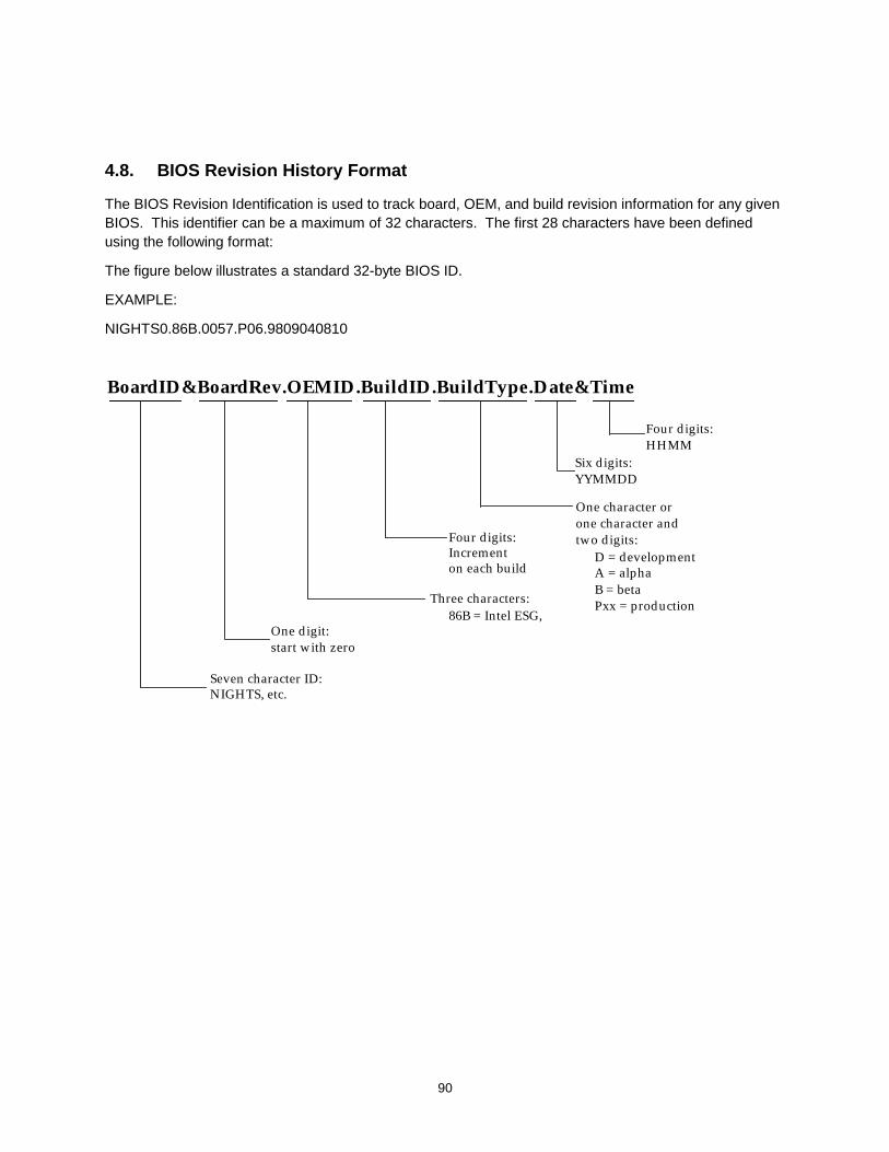
90
4.8. BIOS Revision History Format
The BIOS Revision Identification is used to track board, OEM, and build revision information for any givenBIOS. This identifier can be a maximum of 32 characters. The first 28 characters have been definedusing the following format:
The figure below illustrates a standard 32-byte BIOS ID.
EXAMPLE:
NIGHTS0.86B.0057.P06.9809040810
BoardID&BoardRev.OEMID.BuildID.BuildType.Date&Time
Four digits:HHMM
Six digits:YYMMDD
One character orone character andtwo digits:
A = alphaB = betaPxx = production
D = developmentFour digits:Incrementon each build
Three characters:86B = Intel ESG,
One digit:start with zero
Seven character ID:NIGHTS, etc.
91
5. System Setup Utility / Configuration Utility
This chapter describes the Configuration Utilities that provide the means to configure on board resourcesand add-in cards. The utilities are provided in two forms: the diskette-loadable SSU and the ROM-residentBIOS Setup utility. The following topics are covered here:
• Configuration utilities overview
• Configurable options
• BIOS Setup utility operation
• Configuration CMOS RAM definition
5.1 Configuration Utilities Overview
Configuration of on board devices is done using the BIOS Setup utility embedded in Flash ROM. Setupprovides enough configuration functionality to boot a system diskette, shipped with the hardware, thatcontains the SSU. The booted SSU is required for configuration of PCI and ISA add-in cards. The SSU isreleased on diskette or CDROM. Setup is always provided in Flash for basic system configuration.
The SSU is PCI-aware and conforms to the ISA Plug and Play Specification version 1.1. The SSU workswith any compliant CFG or OVL files supplied by the peripheral device manufacturer. Intel supplies onlythe OVL and CFG files for the system baseboard.
The configuration utilities modify the CMOS RAM and NVRAM, under direction of the user. The actualhardware configuration is accomplished by the BIOS POST routines and the BIOS Plug-N-Play Auto-Configuration Manager. The configuration utilities always update a checksum for both areas, so that anypotential data corruption is detectable by the BIOS, before actual hardware configuration takes place. Ifthe data is corrupted, the BIOS requests that you configure the system before the system is rebooted.
If the disk-based SSU is used, a logo is automatically displayed before the SSU is executed. The logo canbe customized by the OEM.
5.2 Configurable Options
The following table defines most of the configurable options available in the SSU. More options may alsobe supported.
Note that the BIOS detects the state of the “CMOS default” jumper (on the baseboard). If set prior topower-on or hard reset, the BIOS changes CMOS and NVRAM settings to their default state. Thisguarantees the system’s ability to boot from floppy (CMOS clear) to execute the SSU. The default valuesare highlighted.
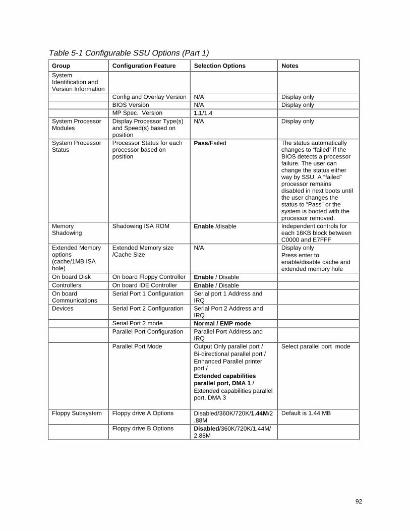
92
Table 5-1 Configurable SSU Options (Part 1)
Group Configuration Feature Selection Options Notes
SystemIdentification andVersion Information
Config and Overlay Version N/A Display onlyBIOS Version N/A Display onlyMP Spec. Version 1.1/1.4
System ProcessorModules
Display Processor Type(s)and Speed(s) based onposition
N/A Display only
System ProcessorStatus
Processor Status for eachprocessor based onposition
Pass/Failed The status automaticallychanges to “failed” if theBIOS detects a processorfailure. The user canchange the status eitherway by SSU. A “failed”processor remainsdisabled in next boots untilthe user changes thestatus to “Pass” or thesystem is booted with theprocessor removed.
MemoryShadowing
Shadowing ISA ROM Enable /disable Independent controls foreach 16KB block betweenC0000 and E7FFF
Extended Memoryoptions(cache/1MB ISAhole)
Extended Memory size/Cache Size
N/A Display onlyPress enter toenable/disable cache andextended memory hole
On board Disk On board Floppy Controller Enable / DisableControllers On board IDE Controller Enable / DisableOn boardCommunications
Serial Port 1 Configuration Serial port 1 Address andIRQ
Devices Serial Port 2 Configuration Serial Port 2 Address andIRQ
Serial Port 2 mode Normal / EMP modeParallel Port Configuration Parallel Port Address and
IRQParallel Port Mode Output Only parallel port /
Bi-directional parallel port /Enhanced Parallel printerport /Extended capabilitiesparallel port, DMA 1 /Extended capabilities parallelport, DMA 3
Select parallel port mode
Floppy Subsystem Floppy drive A Options Disabled/360K/720K/1.44M/2.88M
Default is 1.44 MB
Floppy drive B Options Disabled/360K/720K/1.44M/2.88M
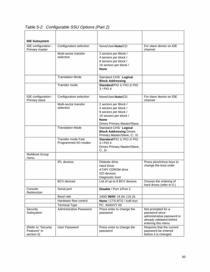
93
Table 5-2. Configurable SSU Options (Part 2)
IDE Subsystem
IDE configuration -Primary master
Configuration selection None/User/Auto/CD For slave device on IDEchannel
Multi-sector transferselection
2 sectors per Block /4 sectors per block /8 sectors per block /16 sectors per block /None,
Translation Mode Standard CHS/ LogicalBlock Addressing
Transfer mode Standard/PIO 1/ PIO 2/ PIO3 / PIO 4
IDE configuration -Primary slave
Configuration selection None/User/Auto/CD For slave device on IDEchannel
Multi-sector transferselection
2 sectors per Block /4 sectors per block /8 sectors per block /16 sectors per block /NoneDrives Primary Master/Slave,
Translation Mode Standard CHS/ LogicalBlock Addressing DrivesPrimary Master/Slave, C:, D:
Transfer mode FastProgrammed I/O modes
Standard/PIO 1/ PIO 2/ PIO3 / PIO 4Drives Primary Master/Slave,C:, D:
Multiboot Groupmenu
IPL devices Diskette driveHard DriveATAPI CDROM driveI2O devicesDiagnostic boot
Press plus/minus keys tochange the boot order
BCV devices List of up to 8 BCV devices Choose the ordering ofhard drives (refer to 0 )
ConsoleRedirection
Serial port Disable / Port 1/Port 2
Baud rate 2400/ 9600/ 19.2k/ 115.2kHardware flow control None / CTS-RTS / Xoff-XonTerminal Type PC ANSI/VT 00
SecuritySubsystem
Administrative Password Press enter to change thepassword
Not prompted for apassword sinceadministrative password isalready validated beforeentering this menu
(Refer to “SecurityFeatures” insection 0)
User Password Press enter to change thepassword
Requires that the currentpassword be enteredbefore it is changed

94
Secure Mode Hotkey Ctrl-Alt-key or None This is the key to presswith Ctrl-Alt keys to entersecure mode immediately.Valid keys are A-Z, 0-9
Secure Boot Mode Enable / DisableVideo Blanking Enable / DisableReset Button and PowerSwitch Locking
Enable / Disable Firmware/bios onlysupports enable.
Keyboard Inactivity Timer 2 min/ 5 min. / 10 min / 20min / 1 hr / 2 hr
Floppy Writes DuringSecure Mode
Enable / Disable
Password on boot Disabled/EnabledOn board SCSISubsystem
On board SCSI ROM Scan Enable / Disable All on board SCSI fullyconfigured, but ROM scanskipped if disabled
Language Support Language Support options English/Italian/Spanish/French/German
OEM may replace any ofthese languages withanother
Keyboard/Mouse NumLock State at Boot On / OffSubsystem Typematic Speed Slow / Medium / Fast
Mouse Control Enabled/Disabled
95
Table 5-3 Configurable SSU Options (Part 3)
ServerManagement
SystemManagementOptions
SMM Enable Enable / Disable
Event Logging Enable / Disable Controls on board eventlogging.
5.3. Setup Utility Operation
The ROM-resident Setup utility configures only on board devices. Configuration of added PCI or ISA cardsrequires the use of the diskette-loadable SSU.
The Setup utility screen is divided into four functional areas:
Keyboard Command Bar Located at the bottom of the screen. This bar displays thekeyboard commands supported by the Setup utility.
Menu Selection Bar Located at the top of the screen. Displays the various major menuselections available to the user. The Server Setup utility majormenus are: Main Menu, Advanced Menu, Security Menu, ServerMenu, Boot Menu, and the Exit Menu.
Options Menu Each Options menu occupies the left and center sections of thescreen. Each menu contains a set of features. Selecting certainfeatures within a major Options menu drops you into sub-menus.
Item Specific Help Screen Located at the right side of the screen is an item-specific Helpscreen.
5.3.1. Entering Setup UtilityDuring POST operation, the user is prompted to enter Setup using the F2 function key as follows:
Press <F2> to enter Setup
Note that a few seconds might pass before Setup is entered. This is the result of POST completing testand initialization functions that must be completed before Setup can be entered. When Setup is entered,the Main Menu options page is displayed.
5.3.2 Keyboard Command BarThe bottom portion of the Setup screen provides a list of commands that are used for navigating the SetupUtility. These commands are displayed at all times, for every menu and sub-menu.
Each Setup menu page contains a number of features. Except those used for informative purposes, eachfeature is associated with a value field. This field contains user-selectable parameters. Depending on thesecurity option chosen and in effect via password, a menu feature’s value can be changeable or not. If a

96
value is non-changeable due to insufficient security privilege (or other reasons), the feature’s value field isinaccessible. The Keyboard Command Bar supports the following:
F1 Help
Pressing F1 on any menu invokes the general Help window. This window describes the Setup key legend.The up arrow, down arrow, Page Up, Page Down, Home, and End keys scrolls the text in this window.
Enter Execute Command
The Enter key is used to activate sub-menus when the selected feature is a sub-menu, or to display a picklist if a selected feature has a value field, or to select a sub-field for multi-valued features like time anddate. If a pick list is displayed, the Enter key will undo the pick list, and allow another selection in theparent menu.
ESC Exit
The ESC key provides a mechanism for backing out of any field. This key will undo the pressing of theEnter key. When the ESC key is pressed while editing any field or selecting features of a menu, the parentmenu is re-entered. When the ESC key is pressed in any sub-menu, the parent menu is re-entered. Whenthe ESC key is pressed in any major menu, the Exit menu page displays.
↑ Select Item
The up arrow is used to select the previous value in a pick list, or the previous feature in a menu item’soption list. The selected item must then be activated by pressing the Enter key.
↓ Select Item
The down arrow is used to select the next value in a menu item’s option list, or a value field’s pick list. Theselected item must then be activated by pressing the Enter key.
↔ Select Menu
The left and right arrow keys are used to move between the major menu pages. The keys have no affect ifa sub-menu or pick list is displayed.
- Change Value
The minus key is used to change the value of the current item to the previous value. This key scrollsthrough the values in the associated pick list without displaying the full list.
+ Change Value
The plus key is used to change the value of the current menu item to the next value. This key scrollsthrough the values in the associated pick list without displaying the full list.
F9 Setup Defaults
Pressing F9 causes the following to appear:
97
Setup Confirmation
Load default configuration now?
[Yes] [No]
If the “Yes” is selected and the Enter key is pressed, all Setup fields are set to their default values. If “No”is selected and the Enter key is pressed, or if the ESC key is pressed, then you are returned to where youwere before F9 was pressed without affecting any existing field values.
F10 Save and Exit
Pressing F10 causes the following message to appear:
Setup Confirmation
Save Configuration changes and exit now?
[Yes] [NO]
If “Yes” is selected and the Enter key is pressed, all changes are saved and Setup is exited. If “No” isselected and the Enter key is pressed, or the ESC key is pressed, you are returned to where you werebefore F10 was pressed without affecting any existing values.
5.3.3 Menu Selection BarThe Menu Selection Bar is located at the top of the screen. It displays the various major menu selectionsavailable to the user:
• Main Menu
• Advanced Menu
• Security Menu
• Server Menu
• Boot Menu
• Exit Menu
These and associated sub-menus are described below.
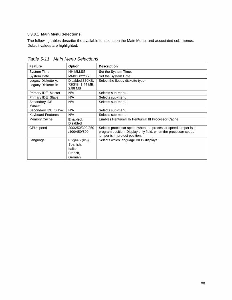
98
5.3.3.1 Main Menu Selections
The following tables describe the available functions on the Main Menu, and associated sub-menus.Default values are highlighted.
Table 5-11. Main Menu Selections
Feature Option Description
System Time HH:MM:SS Set the System Time.System Date MM/DD/YYYY Set the System Date.Legacy Diskette A:Legacy Diskette B:
Disabled,360KB,720KB, 1.44 MB,2.88 MB
Select the floppy diskette type.
Primary IDE Master N/A Selects sub-menu.Primary IDE Slave N/A Selects sub-menu.Secondary IDEMaster
N/A Selects sub-menu.
Secondary IDE Slave N/A Selects sub-menu.Keyboard Features N/A Selects sub-menu.Memory Cache Enabled,
DisabledEnables Pentium® II/ Pentium® III Processor Cache
CPU speed 200/250/300/350/400/450/500
Selects processor speed when the processor speed jumper is inprogram position. Display only field, when the processor speedjumper is in protect position.
Language English (US),Spanish,Italian,French,German
Selects which language BIOS displays.

99
Table 5-12. Primary IDE Master and Slave Adapters Sub-menu Selections
Feature Option Description
Type AutoNoneCDROMUser
Auto allows the system to attempt auto-detection of the drive type.None informs the system to ignore this drive.CDROM allows the manual entry of fields described below.User allows the manual entry of all fields described below.
Cylinders 1 to 9999 Number of Cylinders on Drive. This field is only changeable for Type User.This field is informational only, for Type Auto.*
Heads 1 to 16 Number of read/write heads on Drive.This field is only available for Type User.This field is informational only, for Type Auto.*
Sectors 0 to 63 Number of Sectors per Track. This field only available for Type User.This field is informational only, for Type Auto.*
Maximum Capacity seedescription
Computed size of Drive from Cylinders, Heads, and Sectors entered.This field is only available for Type User.This field is informational only, for Type Auto.*
LBA Format information onlyTotal Sectors information onlyMaximum Capacity information onlyMulti-Sector Transfer Disabled
2, 4, 8, or16 Sectors
Determines the number of sectors per block for multiple sector transfers.This field is informational only, for Type Auto.
LBA Mode Control DisabledEnabled
Enabling LBA causes Logical Block Addressing to be used in place ofCylinders, Heads, and Sectors.This field is informational only, for Type Auto.
32 Bit I/O DisabledEnabled
Enabling allows 32 bit IDE data transfers.This field is informational only, for Type Auto.
Transfer Mode StandardFast PIO 1Fast PIO 2Fast PIO 3Fast PIO 4
Select the method for moving data to/from the drive.This field is informational only, for Type Auto.
Ultra DMA DisabledEnabled
For use with Ultra DMA drives.This field is informational only, for Type Auto.
* These fields appear only for Type Auto if a drive is detected.
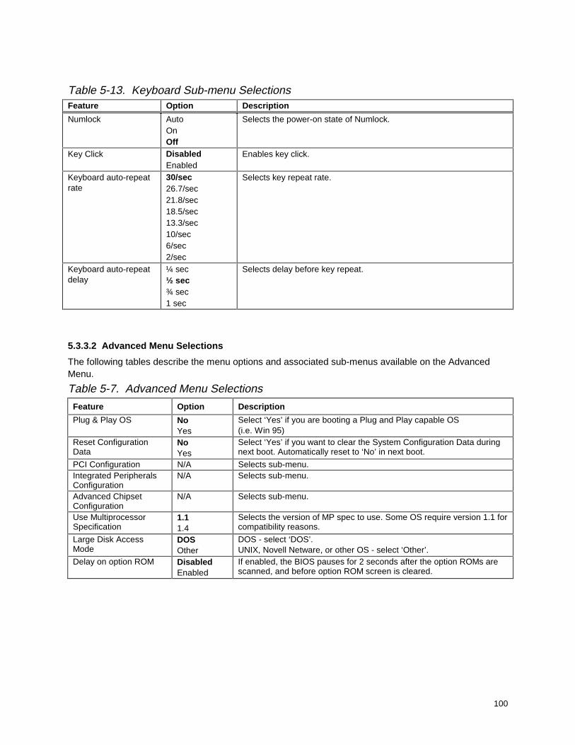
100
Table 5-13. Keyboard Sub-menu SelectionsFeature Option Description
Numlock AutoOnOff
Selects the power-on state of Numlock.
Key Click DisabledEnabled
Enables key click.
Keyboard auto-repeatrate
30/sec26.7/sec21.8/sec18.5/sec13.3/sec10/sec6/sec2/sec
Selects key repeat rate.
Keyboard auto-repeatdelay
¼ sec½ sec¾ sec1 sec
Selects delay before key repeat.
5.3.3.2 Advanced Menu Selections
The following tables describe the menu options and associated sub-menus available on the AdvancedMenu.
Table 5-7. Advanced Menu Selections
Feature Option Description
Plug & Play OS NoYes
Select ‘Yes’ if you are booting a Plug and Play capable OS(i.e. Win 95)
Reset ConfigurationData
NoYes
Select ‘Yes’ if you want to clear the System Configuration Data duringnext boot. Automatically reset to ‘No’ in next boot.
PCI Configuration N/A Selects sub-menu.Integrated PeripheralsConfiguration
N/A Selects sub-menu.
Advanced ChipsetConfiguration
N/A Selects sub-menu.
Use MultiprocessorSpecification
1.11.4
Selects the version of MP spec to use. Some OS require version 1.1 forcompatibility reasons.
Large Disk AccessMode
DOSOther
DOS - select ‘DOS’.UNIX, Novell Netware, or other OS - select ‘Other’.
Delay on option ROM DisabledEnabled
If enabled, the BIOS pauses for 2 seconds after the option ROMs arescanned, and before option ROM screen is cleared.
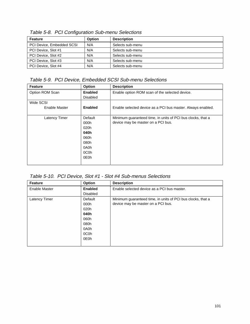
101
Table 5-8. PCI Configuration Sub-menu SelectionsFeature Option Description
PCI Device, Embedded SCSI N/A Selects sub-menuPCI Device, Slot #1 N/A Selects sub-menuPCI Device, Slot #2 N/A Selects sub-menuPCI Device, Slot #3 N/A Selects sub-menuPCI Device, Slot #4 N/A Selects sub-menu
Table 5-9. PCI Device, Embedded SCSI Sub-menu SelectionsFeature Option Description
Option ROM Scan EnabledDisabled
Enable option ROM scan of the selected device.
Wide SCSIEnable Master Enabled Enable selected device as a PCI bus master. Always enabled.
Latency Timer Default000h020h040h060h080h0A0h0C0h0E0h
Minimum guaranteed time, in units of PCI bus clocks, that adevice may be master on a PCI bus.
Table 5-10. PCI Device, Slot #1 - Slot #4 Sub-menus SelectionsFeature Option Description
Enable Master EnabledDisabled
Enable selected device as a PCI bus master.
Latency Timer Default000h020h040h060h080h0A0h0C0h0E0h
Minimum guaranteed time, in units of PCI bus clocks, that adevice may be master on a PCI bus.
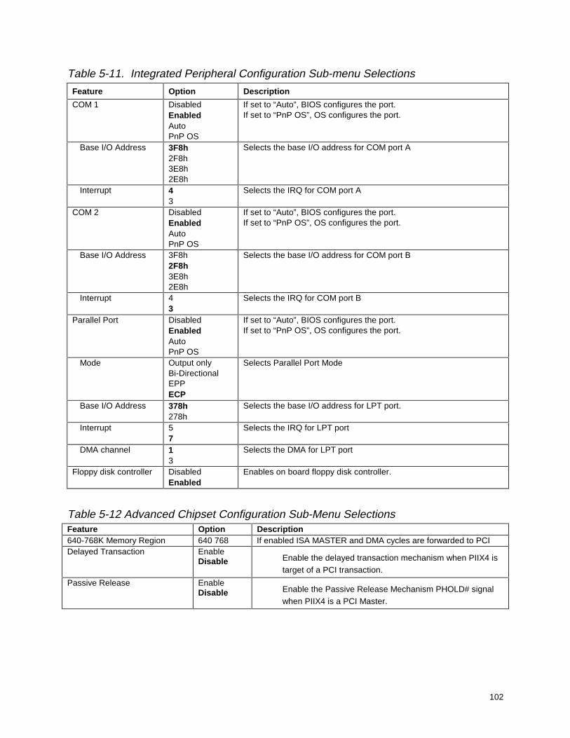
102
Table 5-11. Integrated Peripheral Configuration Sub-menu Selections
Feature Option Description
COM 1 DisabledEnabledAutoPnP OS
If set to “Auto”, BIOS configures the port.If set to “PnP OS”, OS configures the port.
Base I/O Address 3F8h2F8h3E8h2E8h
Selects the base I/O address for COM port A
Interrupt 43
Selects the IRQ for COM port A
COM 2 DisabledEnabledAutoPnP OS
If set to “Auto”, BIOS configures the port.If set to “PnP OS”, OS configures the port.
Base I/O Address 3F8h2F8h3E8h2E8h
Selects the base I/O address for COM port B
Interrupt 43
Selects the IRQ for COM port B
Parallel Port DisabledEnabledAutoPnP OS
If set to “Auto”, BIOS configures the port.If set to “PnP OS”, OS configures the port.
Mode Output onlyBi-DirectionalEPPECP
Selects Parallel Port Mode
Base I/O Address 378h278h
Selects the base I/O address for LPT port.
Interrupt 57
Selects the IRQ for LPT port
DMA channel 13
Selects the DMA for LPT port
Floppy disk controller DisabledEnabled
Enables on board floppy disk controller.
Table 5-12 Advanced Chipset Configuration Sub-Menu SelectionsFeature Option Description640-768K Memory Region 640 768 If enabled ISA MASTER and DMA cycles are forwarded to PCIDelayed Transaction Enable
Disable Enable the delayed transaction mechanism when PIIX4 istarget of a PCI transaction.
Passive Release EnableDisable Enable the Passive Release Mechanism PHOLD# signal
when PIIX4 is a PCI Master.

103
5.3.3.3 Security Menu Selections
The following options are available on the Security Menu.
Table 3-13. Security Menu Selections
Feature Option Description
User Password is ClearSet
Status only; user cannot modify. Once set, it can be disabled bysetting to a null string, or clearing via the clear password jumperon board.
Administrator Password is Clear Set Status only; user cannot modify. Once set, it can be disabled bysetting to a null string, or clearing via the clear password jumperon board.
Set User Password is Press Enter When the Enter key is pressed, the user is prompted for apassword; press ESC key to abort. Once set, can be disabled bysetting to a null string, or clearing via the clear password jumperon board
Set Administrator Passwordis
Press Enter When the Enter key is pressed, the user is prompted for apassword; press ESC key to abort. Once set, can be disabled bysetting to a null string, or clearing via the clear password jumperon board
Password on boot DisabledEnabled
If enabled, and the user password is set, the system will promptthe user for a password before system boots.
Diskette Access UserAdmin
User is prevented from accessing the floppy drive if set to Admin.Administrator is always prevented from accessing the floppydrive.
Fixed disk boot sector NormalWrite protect
Will write protect the boot sector of the hard drive to preventviruses from corrupting the drive under DOS if set to writeprotect.
Secure Mode Timer Disabled2 min, 5 min,10 min, 20min, 1 hr, 2 hr
Period of keyboard and PS/2 mouse inactivity specified forSecure Mode to activate. A password is required for SecureMode to function. Cannot be enabled unless at least onepassword is enabled.
Secure Mode Hot Key(Ctrl-Alt- )
[ ][A, B, ..., Z][0-9]
Key assigned to invoke the secure mode feature. Cannot beenabled unless at least one password is enabled. Can bedisabled by entering a new key followed by a backspace.
Secure Mode Boot DisabledEnabled
System boots in Secure Mode. The user must enter a passwordto unlock the system. Cannot be enabled unless at least onepassword is enabled.
Video Blanking DisabledEnabled
Blank video when Secure mode is activated. A password isrequired to unlock the system. Cannot be enabled unless at leastone password is enabled.
Floppy Write Protect DisabledEnabled
When Secure mode is activated, the floppy drive is writeprotected. A password is required to re-enable floppy writes.Cannot be enabled unless at least one password is enabled.
Reset and Power SwitchLock
DisabledEnabled
When Secure Mode is activated, the Reset and Power switchesare locked. A password is required to unlock the system. Cannotbe enabled unless at least one password is enabled.
System backup reminder DisabledDailyWeeklyMonthly
Before booting the BIOS, the gives the user a reminder toperform system backup if set.
Virus check reminder DisabledDailyWeeklyMonthly
Before booting the BIOS, this gives the user a reminder toperform a virus check if set.
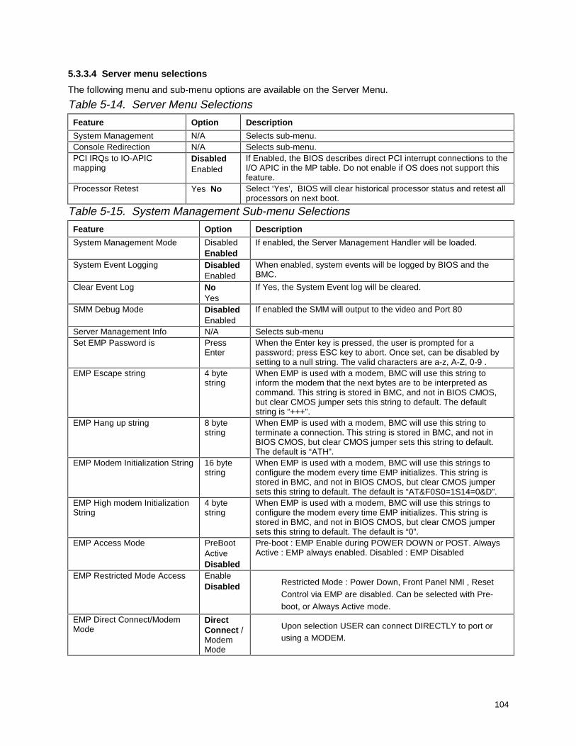
104
5.3.3.4 Server menu selections
The following menu and sub-menu options are available on the Server Menu.
Table 5-14. Server Menu Selections
Feature Option Description
System Management N/A Selects sub-menu.Console Redirection N/A Selects sub-menu.PCI IRQs to IO-APICmapping
DisabledEnabled
If Enabled, the BIOS describes direct PCI interrupt connections to theI/O APIC in the MP table. Do not enable if OS does not support thisfeature.
Processor Retest Yes No Select ‘Yes’, BIOS will clear historical processor status and retest allprocessors on next boot.
Table 5-15. System Management Sub-menu Selections
Feature Option Description
System Management Mode DisabledEnabled
If enabled, the Server Management Handler will be loaded.
System Event Logging DisabledEnabled
When enabled, system events will be logged by BIOS and theBMC.
Clear Event Log NoYes
If Yes, the System Event log will be cleared.
SMM Debug Mode DisabledEnabled
If enabled the SMM will output to the video and Port 80
Server Management Info N/A Selects sub-menuSet EMP Password is Press
EnterWhen the Enter key is pressed, the user is prompted for apassword; press ESC key to abort. Once set, can be disabled bysetting to a null string. The valid characters are a-z, A-Z, 0-9 .
EMP Escape string 4 bytestring
When EMP is used with a modem, BMC will use this string toinform the modem that the next bytes are to be interpreted ascommand. This string is stored in BMC, and not in BIOS CMOS,but clear CMOS jumper sets this string to default. The defaultstring is “+++”.
EMP Hang up string 8 bytestring
When EMP is used with a modem, BMC will use this string toterminate a connection. This string is stored in BMC, and not inBIOS CMOS, but clear CMOS jumper sets this string to default.The default is “ATH”.
EMP Modem Initialization String 16 bytestring
When EMP is used with a modem, BMC will use this strings toconfigure the modem every time EMP initializes. This string isstored in BMC, and not in BIOS CMOS, but clear CMOS jumpersets this string to default. The default is “AT&F0S0=1S14=0&D”.
EMP High modem InitializationString
4 bytestring
When EMP is used with a modem, BMC will use this strings toconfigure the modem every time EMP initializes. This string isstored in BMC, and not in BIOS CMOS, but clear CMOS jumpersets this string to default. The default is “0”.
EMP Access Mode PreBootActiveDisabled
Pre-boot : EMP Enable during POWER DOWN or POST. AlwaysActive : EMP always enabled. Disabled : EMP Disabled
EMP Restricted Mode Access EnableDisabled Restricted Mode : Power Down, Front Panel NMI , Reset
Control via EMP are disabled. Can be selected with Pre-boot, or Always Active mode.
EMP Direct Connect/ModemMode
DirectConnect /ModemMode
Upon selection USER can connect DIRECTLY to port orusing a MODEM.
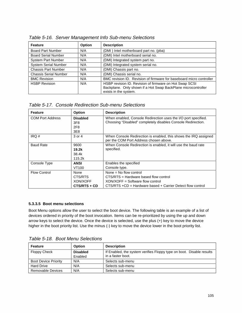
105
Table 5-16. Server Management Info Sub-menu Selections
Feature Option Description
Board Part Number N/A (DMI ) Intel motherboard part no. (pba)Board Serial Number N/A (DMI) Intel motherboard serial no.System Part Number N/A (DMI) Integrated system part no.System Serial Number N/A (DMI) Integrated system serial no.Chassis Part Number N/A (DMI) Chassis part no.Chassis Serial Number N/A (DMI) Chassis serial no.BMC Revision N/A BMC revision ID. Revision of firmware for baseboard micro controllerHSBP Revision N/A HSBP revision ID. Revision of firmware on Hot Swap SCSI
Backplane. Only shown if a Hot Swap BackPlane microcontrollerexists in the system.
Table 5-17. Console Redirection Sub-menu Selections
Feature Option Description
COM Port Address Disabled3F82F83E8
When enabled, Console Redirection uses the I/O port specified.Choosing “Disabled” completely disables Console Redirection.
IRQ # 3 or 4 When Console Redirection is enabled, this shows the IRQ assignedper the COM Port Address chosen above.
Baud Rate 960019.2k38.4k115.2k
When Console Redirection is enabled, it will use the baud ratespecified.
Console Type ANSIVT100
Enables the specifiedConsole type.
Flow Control NoneCTS/RTSXON/XOFFCTS/RTS + CD
None = No flow controlCTS/RTS = Hardware based flow controlXON/XOFF = Software flow controlCTS/RTS +CD = Hardware based + Carrier Detect flow control
5.3.3.5 Boot menu selections
Boot Menu options allow the user to select the boot device. The following table is an example of a list ofdevices ordered in priority of the boot invocation. Items can be re-prioritized by using the up and downarrow keys to select the device. Once the device is selected, use the plus (+) key to move the devicehigher in the boot priority list. Use the minus (-) key to move the device lower in the boot priority list.
Table 5-18. Boot Menu Selections
Feature Option Description
Floppy Check DisabledEnabled
If Enabled, the system verifies Floppy type on boot. Disable resultsin a faster boot.
Boot Device Priority N/A Selects sub-menuHard Drive N/A Selects sub-menuRemovable Devices N/A Selects sub-menu
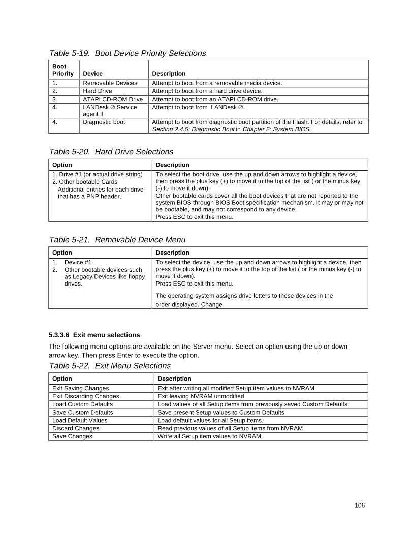
106
Table 5-19. Boot Device Priority Selections
BootPriority Device Description
1. Removable Devices Attempt to boot from a removable media device.2. Hard Drive Attempt to boot from a hard drive device.3. ATAPI CD-ROM Drive Attempt to boot from an ATAPI CD-ROM drive.4. LANDesk ® Service
agent IIAttempt to boot from LANDesk ®.
4. Diagnostic boot Attempt to boot from diagnostic boot partition of the Flash. For details, refer toSection 2.4.5: Diagnostic Boot in Chapter 2: System BIOS.
Table 5-20. Hard Drive Selections
Option Description
1. Drive #1 (or actual drive string)2. Other bootable Cards
Additional entries for each drivethat has a PNP header.
To select the boot drive, use the up and down arrows to highlight a device,then press the plus key (+) to move it to the top of the list ( or the minus key(-) to move it down).Other bootable cards cover all the boot devices that are not reported to thesystem BIOS through BIOS Boot specification mechanism. It may or may notbe bootable, and may not correspond to any device.Press ESC to exit this menu.
Table 5-21. Removable Device Menu
Option Description
1. Device #12. Other bootable devices such
as Legacy Devices like floppydrives.
To select the device, use the up and down arrows to highlight a device, thenpress the plus key (+) to move it to the top of the list ( or the minus key (-) tomove it down).Press ESC to exit this menu.
The operating system assigns drive letters to these devices in the
order displayed. Change
5.3.3.6 Exit menu selections
The following menu options are available on the Server menu. Select an option using the up or downarrow key. Then press Enter to execute the option.
Table 5-22. Exit Menu Selections
Option Description
Exit Saving Changes Exit after writing all modified Setup item values to NVRAMExit Discarding Changes Exit leaving NVRAM unmodifiedLoad Custom Defaults Load values of all Setup items from previously saved Custom DefaultsSave Custom Defaults Save present Setup values to Custom DefaultsLoad Default Values Load default values for all Setup items.Discard Changes Read previous values of all Setup items from NVRAMSave Changes Write all Setup item values to NVRAM
107
6. Flash Update Utility
The Flash Memory Update utility (IFLASH) loads a fresh copy of the BIOS into Flash ROM. The loadedcode and data include the following:
• On board Video BIOS and SCSI BIOS
• BIOS Setup utility
• User-definable Flash area (User Binary Area)
• Diagnostic boot loader binary
• Language file
When running IFLASH in interactive mode, you may choose to update a particular Flash area. Updating aFlash area takes a file or series of files from a hard or floppy disk, and loads it in the specified area ofFlash ROM. In interactive mode, IFLASH can display the header information of the selected files.
NOTEThe utility iFLASH must be run without the presence of a Protected mode controlprogram, such as Windows or EMM386 (Do not run in a DOS window under NT, Win95or Win98. IFLASH uses the processor’s flat addressing mode to update the Flash part.
Other platforms have shown interactions between system sensor event logging, and the IFLASH. With theNightshade, Sensor event logging is not performed via SMI, thus there are no potential interactions toeffect/corrupt FLASH.
6.1 Loading the System BIOS
A new BIOS is contained in .BIx files. The number of .BIx files is determined by the size of the BIOS areain the Flash part. For further information on logical area 1 - System BIOS, see Table 4-1: Flash Table. Asof this writing, the system BIOS area is 8 files (512KB). They are named as follows:
xxxxxxxx.BIO
xxxxxxxx.BI1
xxxxxxxx.BI2
etc til xxxxxx.BI7
The first 8 letters of each filename on the release diskette can be any value, but cannot be renamed. Eachfile contains a link to the next file in the sequence. IFLASH does a link check before updating to ensurethat the process is successful. However, the first file in the list can be renamed, but all subsequentfilenames must remain unchanged. (See Section 6.5: Recovery Mode in Chapter 6: Flash Update Utility.)
Once an update of the system BIOS is complete, you are prompted for a reboot. Language files areoverwritten by updating the system BIOS. If a custom language file has been created, it must be Flashedin after the system BIOS has been updated. The user binary area and diagnostic loader binary image isalso updated during a system BIOS update. User binary can be updated independent of the system BIOS.
108
6.2 User Binary Area
Nightshade includes an 8KB area in Flash for implementation-specific OEM add-ons. The User Binaryarea can be saved and updated exactly as described above in the System BIOS section. Only one file isneeded. The valid extension for user files is USR.
6.3 Diagnostic Boot Loader Partition
Nightshade supports 32KB of diagnostic boot loader, which can be saved and updated like the UserBinary area, without having to update the rest of the BIOS. The valid extension for the diagnostic bootloader partition is .DBL.
6.4 Language Area
The system BIOS language area can be updated without having to update the entire BIOS. Nightshadesupports English, Spanish, French, German, and Italian (from Intel). These languages are selectableusing the SSU . When additional language files (*.LNG) are made available, they can be loaded into thesystem BIOS using IFLASH (in interactive mode, as described above), in the same manner as updatingthe system BIOS and the user binaries.
6.5 Recovery Mode
In the case of a corrupt .BIx image or an unsuccessful update of the system BIOS, Nightshade can boot inrecovery mode. To place Nightshade into recovery mode, move the boot option jumper to recoveryposition. The jumper connects pins 1 and 2 (normal BIOS) by default.
Recovery mode requires at least 8 MB of RAM in the first DIMM socket, and drive A: must be set up tosupport a 3.5” 1.44 MB floppy drive. This is the mode of last resort, used only when the main system BIOSwill not come up. In recovery mode operation, IFLASH (in non-interactive mode only) automaticallyupdates only the main system BIOS. IFLASH senses that N440BX is in recovery mode and automaticallyattempts to update the system BIOS. It is recommended to turn off FRB by setting the jumper to disablewhile doing recovery.
Before powering up Nightshade, obtain a bootable MS DOS diskette that contains a copy of the BIOSrelease. Boot the system from drive A: using this diskette, which executes a special AUTOEXEC.BAT filefrom the BIOS release. The batch file invokes IFLASH, which updates the Flash ROM with the BIOSfound on the diskette.
NOTE
During recovery mode, video will not be initialized. One high-pitched beep announces the start of therecovery process. The entire process takes two to four minutes. A successful update ends with two high-pitched beeps. Failure is indicated by a long series of short beeps.
If a failure occurs, it is most likely that one or more of the system BIOS IFLASH files is corrupt or missing.After a successful update, power down the system and move the recovery jumper back to pins 1 and 2.Power up the system and verify that the BIOS version number matches the version of the entire BIOS thatyou originally attempted to update. CMOS is not cleared when the system BIOS is updated.Configuration information like ESCD is not overwritten during BIOS flash update. Remember that any
109
additional or different languages or User Binaries or diagnostic binaries that were present before updatingneed to be reloaded to Flash.
7. Error Handling
This chapter defines how errors are handled by system BIOS on the Nightshade platform. This chapterprovides the role of BIOS in error handling and the interaction between the BIOS, platform hardware andserver management firmware as far as error handling is concerned. In addition, error logging techniquesare described, and beep codes for errors are defined.
7.1 Error Sources and Types
One of the major requirements of server management is to correctly and consistently handle systemerrors. System errors on Nightshade, which can be disabled and enabled individually or as a group, canbe categorized as follows:
• ISA bus
• PCI bus
• Memory single and multi-bit errors
• Sensors
• processor internal error, thermal trip error, temperatures and voltages, GTL voltage levels
The BIOS cannot detect errors on the Pentium® II/ Pentium® III processor bus because PAC does notmonitor these.
ISA and PCI bus errors can be further classified as ‘standard bus’ errors, which have a standard registerinterface across all platforms. All other errors, such as Pentium II/ Pentium III processor and ECC errors,are referred to as ‘product-specific’ errors, which require special consideration depending upon the systemconfiguration. Product-specific errors can be emulated as standard bus errors, if specific routing of certainhardware signals, as documented in this chapter, are followed. This emulation is important to both OS andBIOS NMI handlers, which have no knowledge of product-specific errors, but need to recover and shutdown the system gracefully. In Nightshade, sensors are managed by the BMC. The BMC is capable ofreceiving event messages from individual sensors and log system events. The BIOS programs the BMCnot to generate a SMI on a sensor events such as fan failure.
7.2 Error Handlers
The BIOS has an NMI handler that gets invoked when an NMI occurs in POST. Generally, the OS trapsthe NMI and does not pass it onto the BIOS NMI handler. Therefore, the BIOS NMI handler is rarelyinvoked in real operating environment. The SMI handler cannot be bypassed by the OS, and is used tohandle and log system level events that are not visible to the server management firmware.
7.2.1 BIOS NMI handlerTo maintain DOS compatibility, the BIOS NMI handler only processes enabled standard bus errors, suchas ISA Parity check or IOCHK# errors. It displays an error message, issues a beep signal, and halts. Itdisables NMI using bit 7 of I/O port 70h (RTC Index Port) on the occurrence of an unknown or spuriousNMI. This can cause unusual side effects because it allows a spurious NMI to block a subsequent validNMI.
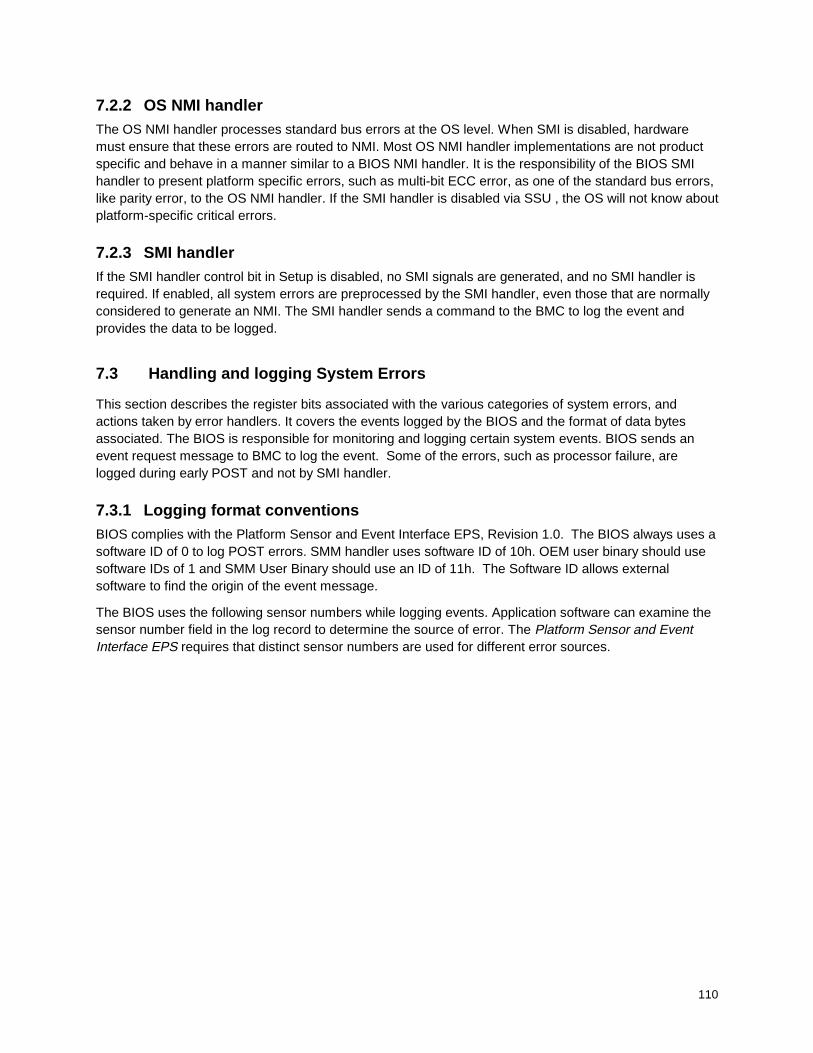
110
7.2.2 OS NMI handlerThe OS NMI handler processes standard bus errors at the OS level. When SMI is disabled, hardwaremust ensure that these errors are routed to NMI. Most OS NMI handler implementations are not productspecific and behave in a manner similar to a BIOS NMI handler. It is the responsibility of the BIOS SMIhandler to present platform specific errors, such as multi-bit ECC error, as one of the standard bus errors,like parity error, to the OS NMI handler. If the SMI handler is disabled via SSU , the OS will not know aboutplatform-specific critical errors.
7.2.3 SMI handlerIf the SMI handler control bit in Setup is disabled, no SMI signals are generated, and no SMI handler isrequired. If enabled, all system errors are preprocessed by the SMI handler, even those that are normallyconsidered to generate an NMI. The SMI handler sends a command to the BMC to log the event andprovides the data to be logged.
7.3 Handling and logging System Errors
This section describes the register bits associated with the various categories of system errors, andactions taken by error handlers. It covers the events logged by the BIOS and the format of data bytesassociated. The BIOS is responsible for monitoring and logging certain system events. BIOS sends anevent request message to BMC to log the event. Some of the errors, such as processor failure, arelogged during early POST and not by SMI handler.
7.3.1 Logging format conventionsBIOS complies with the Platform Sensor and Event Interface EPS, Revision 1.0. The BIOS always uses asoftware ID of 0 to log POST errors. SMM handler uses software ID of 10h. OEM user binary should usesoftware IDs of 1 and SMM User Binary should use an ID of 11h. The Software ID allows externalsoftware to find the origin of the event message.
The BIOS uses the following sensor numbers while logging events. Application software can examine thesensor number field in the log record to determine the source of error. The Platform Sensor and EventInterface EPS requires that distinct sensor numbers are used for different error sources.
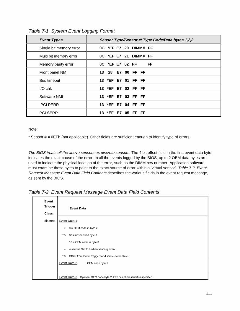
111
Table 7-1. System Event Logging Format
Event Types Sensor Type/Sensor #/ Type Code/Data bytes 1,2,3.
Single bit memory error 0C *EF E7 20 DIMM# FF
Multi bit memory error 0C *EF E7 21 DIMM# FF
Memory parity error 0C *EF E7 02 FF FF
Front panel NMI 13 28 E7 00 FF FF
Bus timeout 13 *EF E7 01 FF FF
I/O chk 13 *EF E7 02 FF FF
Software NMI 13 *EF E7 03 FF FF
PCI PERR 13 *EF E7 04 FF FF
PCI SERR 13 *EF E7 05 FF FF
Note:
* Sensor # = 0EFh (not applicable). Other fields are sufficient enough to identify type of errors.
The BIOS treats all the above sensors as discrete sensors. The 4 bit offset field in the first event data byteindicates the exact cause of the error. In all the events logged by the BIOS, up to 2 OEM data bytes areused to indicate the physical location of the error, such as the DIMM row number. Application softwaremust examine these bytes to point to the exact source of error within a ‘virtual sensor’. Table 7-2, EventRequest Message Event Data Field Contents describes the various fields in the event request message,as sent by the BIOS.
Table 7-2. Event Request Message Event Data Field Contents
Event
Trigger
Class
Event Data
discrete Event Data 1
7 0 = OEM code in byte 2
6:5 00 = unspecified byte 3
10 = OEM code in byte 3
4 reserved. Set to 0 when sending event.
3:0 Offset from Event Trigger for discrete event state
Event Data 2 OEM code byte 1
Event Data 3 Optional OEM code byte 2. FFh or not present if unspecified.
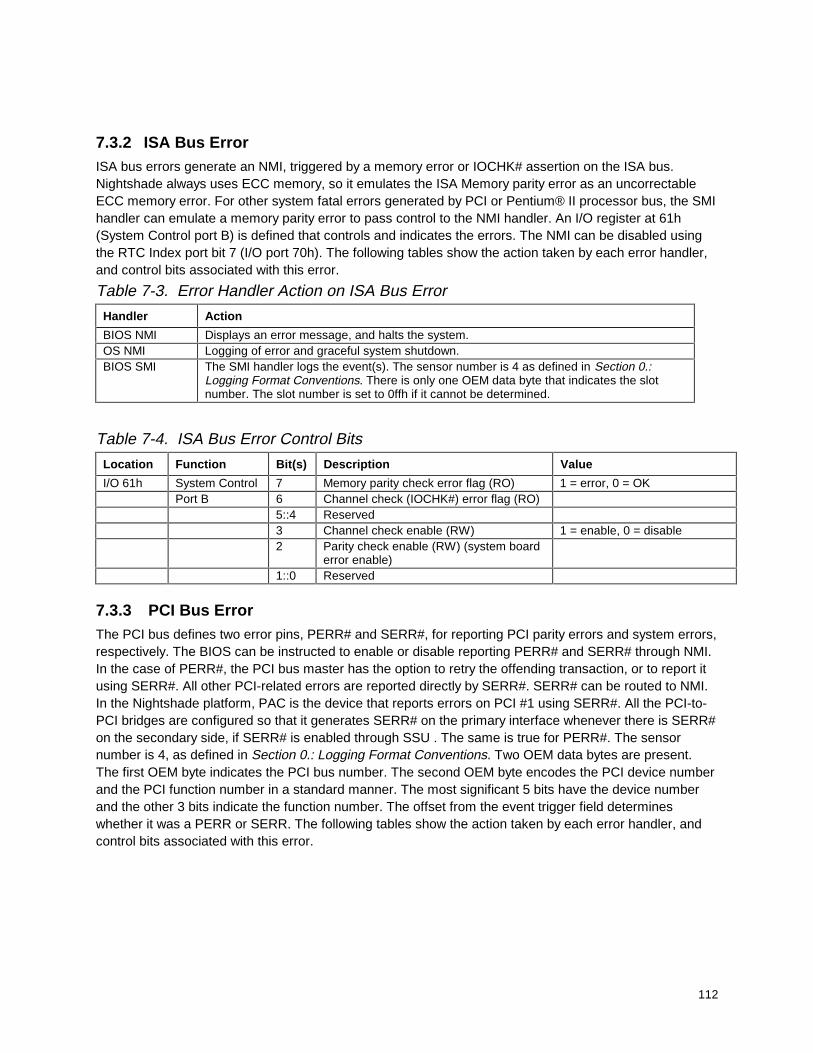
112
7.3.2 ISA Bus ErrorISA bus errors generate an NMI, triggered by a memory error or IOCHK# assertion on the ISA bus.Nightshade always uses ECC memory, so it emulates the ISA Memory parity error as an uncorrectableECC memory error. For other system fatal errors generated by PCI or Pentium® II processor bus, the SMIhandler can emulate a memory parity error to pass control to the NMI handler. An I/O register at 61h(System Control port B) is defined that controls and indicates the errors. The NMI can be disabled usingthe RTC Index port bit 7 (I/O port 70h). The following tables show the action taken by each error handler,and control bits associated with this error.
Table 7-3. Error Handler Action on ISA Bus Error
Handler Action
BIOS NMI Displays an error message, and halts the system.OS NMI Logging of error and graceful system shutdown.BIOS SMI The SMI handler logs the event(s). The sensor number is 4 as defined in Section 0.:
Logging Format Conventions. There is only one OEM data byte that indicates the slotnumber. The slot number is set to 0ffh if it cannot be determined.
Table 7-4. ISA Bus Error Control Bits
Location Function Bit(s) Description Value
I/O 61h System Control 7 Memory parity check error flag (RO) 1 = error, 0 = OKPort B 6 Channel check (IOCHK#) error flag (RO)
5::4 Reserved3 Channel check enable (RW) 1 = enable, 0 = disable2 Parity check enable (RW) (system board
error enable)1::0 Reserved
7.3.3 PCI Bus ErrorThe PCI bus defines two error pins, PERR# and SERR#, for reporting PCI parity errors and system errors,respectively. The BIOS can be instructed to enable or disable reporting PERR# and SERR# through NMI.In the case of PERR#, the PCI bus master has the option to retry the offending transaction, or to report itusing SERR#. All other PCI-related errors are reported directly by SERR#. SERR# can be routed to NMI.In the Nightshade platform, PAC is the device that reports errors on PCI #1 using SERR#. All the PCI-to-PCI bridges are configured so that it generates SERR# on the primary interface whenever there is SERR#on the secondary side, if SERR# is enabled through SSU . The same is true for PERR#. The sensornumber is 4, as defined in Section 0.: Logging Format Conventions. Two OEM data bytes are present.The first OEM byte indicates the PCI bus number. The second OEM byte encodes the PCI device numberand the PCI function number in a standard manner. The most significant 5 bits have the device numberand the other 3 bits indicate the function number. The offset from the event trigger field determineswhether it was a PERR or SERR. The following tables show the action taken by each error handler, andcontrol bits associated with this error.
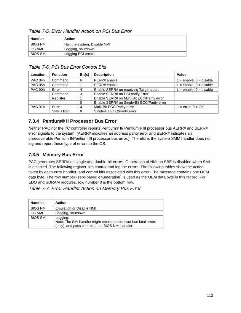
113
Table 7-5. Error Handler Action on PCI Bus Error
Handler Action
BIOS NMI Halt the system, Disable NMIOS NMI Logging, shutdownBIOS SMI Logging PCI errors.
Table 7-6. PCI Bus Error Control Bits
Location Function Bit(s) Description Value
PAC 04h Command 6 PERR# enable 1 = enable, 0 = disablePAC 05h Command 1 SERR# enable 1 = enable, 0 = disablePAC 90h Error 4 Enable SERR# on receiving Target abort 1 = enable, 0 = disable
Command 3 Enable SERR# on PCI parity ErrorRegister 1 Enable SERR# on Multi-Bit ECC/Parity error
0 Enable SERR# on Single-Bit ECC/Parity errorPAC 91h Error 4 Multi-Bit ECC/Parity error 1 = error, 0 = OK
Status Reg. 0 Single-Bit ECC/Parity error
7.3.4 Pentium® II Processor Bus ErrorNeither PAC nor the I2C controller reports Pentium® II/ Pentium® III processor bus AERR# and BERR#error signals to the system. (AERR# indicates an address parity error and BERR# indicates anunrecoverable Pentium II/Pentium III processor bus error.) Therefore, the system SMM handler does notlog and report these type of errors to the OS.
7.3.5 Memory Bus ErrorPAC generates SERR# on single and double-bit errors. Generation of NMI on SBE is disabled when SMIis disabled. The following register bits control and log the errors. The following tables show the actiontaken by each error handler, and control bits associated with this error. The message contains one OEMdata byte. The row number (zero-based enumeration) is used as the OEM data byte in this record. ForEDO and SDRAM modules, row number 0 is the bottom row.
Table 7-7. Error Handler Action on Memory Bus Error
Handler Action
BIOS NMI Emulation or Disable NMIOS NMI Logging, shutdownBIOS SMI Logging.
Note: The SMI handler might emulate processor bus fatal errors(only), and pass control to the BIOS NMI handler.
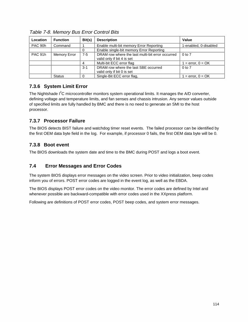
114
Table 7-8. Memory Bus Error Control Bits
Location Function Bit(s) Description Value
PAC 90h Command 1 Enable multi-bit memory Error Reporting 1-enabled, 0-disabled0 Enable single-bit memory Error Reporting
PAC 91h Memory Error 7-5 DRAM row where the last multi-bit error occurredvalid only if bit 4 is set
0 to 7
4 Multi-bit ECC error flag 1 = error, 0 = OK3-1 DRAM row where the last SBE occurred
valid only if bit 0 is set0 to 7
Status 0 Single-Bit ECC error flag, 1 = error, 0 = OK
7.3.6 System Limit ErrorThe Nightshade I2C microcontroller monitors system operational limits. It manages the A/D converter,defining voltage and temperature limits, and fan senses and chassis intrusion. Any sensor values outsideof specified limits are fully handled by BMC and there is no need to generate an SMI to the hostprocessor.
7.3.7 Processor FailureThe BIOS detects BIST failure and watchdog timer reset events. The failed processor can be identified bythe first OEM data byte field in the log. For example, if processor 0 fails, the first OEM data byte will be 0.
7.3.8 Boot eventThe BIOS downloads the system date and time to the BMC during POST and logs a boot event.
7.4 Error Messages and Error Codes
The system BIOS displays error messages on the video screen. Prior to video initialization, beep codesinform you of errors. POST error codes are logged in the event log, as well as the EBDA.
The BIOS displays POST error codes on the video monitor. The error codes are defined by Intel andwhenever possible are backward-compatible with error codes used in the XXpress platform.
Following are definitions of POST error codes, POST beep codes, and system error messages.

115
7.4.1 POST CodesThe BIOS indicates the current testing phase during POST after the video adapter has been successfullyinitialized by writing a 2-digit hex code to I/O location 80h. If a Port-80h card (Post card*) is installed, itdisplays this 2-digit code on a pair of hex display LEDs.
Table 7-9. Port-80h Code Definition
Code Meaning
CP Phoenix check point (port-80) code
The following table contains the port-80 codes displayed during the boot process. A beep code is a seriesof individual beeps on the PC speaker, each of equal length. The following table describes the errorconditions associated with each beep code and the corresponding POST check point code as seen by a‘port 80h’ card (for example, if an error occurs at check point 22h, a beep code of 1-3-1-1 is generated).The - means there s a pause between the sequence that delimits the sequence.

116
Table 7-10. Standard BIOS Port-80 Codes in execution sequence during post
CP Beeps Reason
02 Verify Real Mode12 Restore processor control word during warm boot (only occurs on warm reboot)24 Set ES segment register to 4GB04 Get processor type06 Initialize system hardware18 8254 timer initialization08 Initialize PCIset registers with initial POST valuesC4 Initialize system flags in cmos11 Load alternate registers with initial POST values0E Initialize I/O0C Initialize caches to initial POST values16 1-2-2-3 BIOS ROM checksum17 turn cache off28 Autosize DRAM2A Clear 512K base RAM2C 1-3-4-1 RAM failure on address line xxxx*2E 1-3-4-3 RAM failure on data bits xxxx* of low byte of memory bus (1st 4 meg)2F Initialize L2 cache if enabled in cmos38 Shadow system BIOS ROM20 1-3-1-1 Test DRAM refresh29 Post Memory Manager Initialization (PMM)33 Post Dispatch manager Initialization34 Test CMOSC1 Post error manager Intialization09 Set in POST flag0A Initialize processor registers and cpu microcode3A Autosize cache0B Enable processor cache0F Initialize the local bus IDE (not used anymore but here for phx std)10 Initialize Power Management (APM not used in Nightshade)14 Initialize keyboard controller1A 8237 DMA controller initialization1C Reset Programmable Interrupt Controller22 1-3-1-3 Test 8742 Keyboard Controller32 read processor bus-clock frequency and compute boot processor speed67 Initialize and register other cpu via SMM through apic bus69 Initialize SMI handler for all processors00 wait for secondary processor to execute init smi handlerF4 exit Smi handler (secondary processor executed halt in smi)3C Configure advanced PCIset registers and reset coprocessor3D Load alternate registers with CMOS values42 Initialize interrupt vectors46 2-1-2-3 Check ROM copyright notice45 Initialize all pre-pnp devices49 Initialize PCI bus and devices (also read escd and allocate resources)48 Check video configuration against CMOS (vga or mda)4A Initialize all video adapters in system4C Shadow video BIOS ROM24 put cpu in big real mode (flat mode memory addressing - up to 4 Gb)

117
Table 7-10. Standard BIOS Port-80 Codes (cont.)
CP Beeps Reason
59 Post display manager initialization (video screen error codes now visible)22 reset and test keyboard first try (only warm reset)
52 reset and test keyboard controller (both warm and cold reset)
54 Set key click if enabled
76 Enable keyboard
58 2-2-3-1 Test for unexpected interrupts
4B Quietboot start (not used in N440BX)4E Display copyright notice50 Display cpu(s) type and speed51 Eisa Init (Not used in N440BX)
5A Display prompt “Press F2 to enter SETUP”
5B Disable cpu L1 cache for memory test
5C Test RAM between 512 and 640k
60 Test extended memory (4Mb to top of memory)
62 Test extended memory address lines
64 Jump to UserPatch1
66 Configure advanced cache registers
68 Enable external and processor caches
6A Display external cache size
6C Display shadow message
6E Display non-disposable segments
70 Display error messages to video
72 Check for configuration errors
74 Test real-time clock
7C Set up hardware interrupt vectors
7E Test coprocessor if present
80 not used
88 Initialize BIOS Data Area , timeouts for detecting parallel, serial and hdd controller
clear cmos shutdown flag
8A Initialize Extended BIOS Data Area
81 late post core initialization of devices
87 configure mcd devices
85 Initialize and detect PC-compatible PnP ISA devices (serial, parallel etc)
82 not used
84 clear intrerrupts from com port detection
86 console redirection initialized
83 configure onboard hard disk controller
89 Enable NMI

118
8C Initialize floppy controller
90 Initialize and detect hard disks
8B Detect and test for Mouse or Auxillary device on keyboard controller
95 Install CD-ROM for boot
92 Jump to UserPatch2
C5 Initialize GPNV areas of DMI
98 1-2 Search for option ROMs. One long, two short beeps on checksum failure of an option rom
93 Scan for User flash roms
MP table initialization (wake up secondary processor and halt it)
9C Set up Power Management (not used)
9D enable security
9E Enable hardware interrupts
A0 Set time of day
A2 Check key lock
A4 Initialize typematic rate
C2 Initialize DMI tables
C3 Log post errors with Post error manager and to SEL in BMC
also update VID bits and memory presence to BMC
display and FRB errors (watchdog timeouts, bist or CPU failures)
A8 Erase F2 prompt
AA Scan for F2 key stroke
AC Initialize EMP port if selected. Remove com2 from BDA if EMP is enabled.
Enter SETUP
AE Clear in-POST flag
B0 Turn on secure boot if enabled(secure front panel, blank video, floppy write protect)
Check for errors
B2 POST done – prepare to boot Operating System
B4 1 One short beep before boot
B5 Display Quietboot (not used)
BE Clear screen
B6 Check password (optional)
BC Clear parity checkers
BA not used
B7 ACPI configuration (table configuration in memory and BDA)
BD Display multiboot menu if esc is hit
BF Display system config summary(if enabled in cmos)
8F get total # of hard drives and put in BDA
91 Program IDE hard drives (timing, pio modes etc)
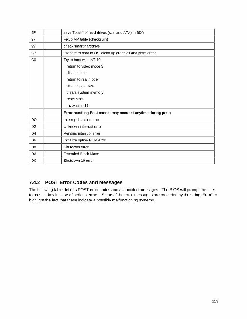
119
9F save Total # of hard drives (scsi and ATA) in BDA
97 Fixup MP table (checksum)
99 check smart harddrive
C7 Prepare to boot to OS, clean up graphics and pmm areas.
C0 Try to boot with INT 19
return to video mode 3
disable pmm
return to real mode
disable gate A20
clears system memory
reset stack
Invokes Int19
Error handling Post codes (may occur at anytime during post)
DO Interrupt handler error
D2 Unknown interrupt error
D4 Pending interrupt error
D6 Initialize option ROM error
D8 Shutdown error
DA Extended Block Move
DC Shutdown 10 error
7.4.2 POST Error Codes and MessagesThe following table defines POST error codes and associated messages. The BIOS will prompt the userto press a key in case of serious errors. Some of the error messages are preceded by the string ‘Error” tohighlight the fact that these indicate a possibly malfunctioning systems.
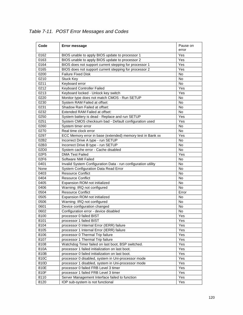
120
Table 7-11. POST Error Messages and Codes
Code Error message Pause onerror
0162 BIOS unable to apply BIOS update to processor 1 Yes0163 BIOS unable to apply BIOS update to processor 2 Yes0164 BIOS does not support current stepping for processor 1 Yes0165 BIOS does not support current stepping for processor 2 Yes0200 Failure Fixed Disk No0210 Stuck Key No0211 Keyboard error No0212 Keyboard Controller Failed Yes0213 Keyboard locked - Unlock key switch Yes0220 Monitor type does not match CMOS - Run SETUP No0230 System RAM Failed at offset: No0231 Shadow Ram Failed at offset: No0232 Extended RAM Failed at offset: No0250 System battery is dead - Replace and run SETUP Yes0251 System CMOS checksum bad - Default configuration used Yes0260 System timer error No0270 Real time clock error No0297 ECC Memory error in base (extended) memory test in Bank xx Yes02B2 Incorrect Drive A type - run SETUP No02B3 Incorrect Drive B type - run SETUP No02D0 System cache error - Cache disabled No02F5 DMA Test Failed Yes02F6 Software NMI Failed No0401 Invalid System Configuration Data - run configuration utility NoNone System Configuration Data Read Error No0403 Resource Conflict No0404 Resource Conflict No0405 Expansion ROM not initialized No0406 Warning: IRQ not configured No0504 Resource Conflict Error0505 Expansion ROM not initialized No0506 Warning: IRQ not configured No0601 Device configuration changed No0602 Configuration error - device disabled No8100 processor 0 failed BIST Yes8101 processor 1 failed BIST Yes8104 processor 0 Internal Error (IERR) failure Yes8105 processor 1 Internal Error (IERR) failure Yes8106 processor 0 Thermal Trip failure Yes8107 processor 1 Thermal Trip failure Yes8108 Watchdog Timer failed on last boot, BSP switched. Yes810A processor 1 failed initialization on last boot. Yes810B processor 0 failed initialization on last boot. Yes810C processor 0 disabled, system in Uni-processor mode Yes810D processor 1 disabled, system in Uni-processor mode Yes810E processor 0 failed FRB Level 3 timer Yes810F processor 1 failed FRB Level 3 timer Yes8110 Server Management Interface failed to function Yes8120 IOP sub-system is not functional Yes

121
8150 NVRAM Cleared by Jumper Yes8151 NVRAM Checksum Error, NVRAM cleared Yes8152 NVRAM Data Invalid, NVRAM cleared Yes
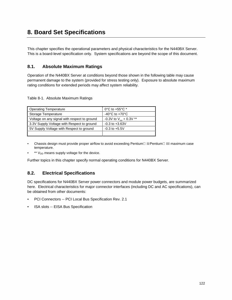
122
8. Board Set Specifications
This chapter specifies the operational parameters and physical characteristics for the N440BX Server.This is a board-level specification only. System specifications are beyond the scope of this document.
8.1. Absolute Maximum Ratings
Operation of the N440BX Server at conditions beyond those shown in the following table may causepermanent damage to the system (provided for stress testing only). Exposure to absolute maximumrating conditions for extended periods may affect system reliability.
Table 8-1. Absolute Maximum Ratings
Operating Temperature 0°C to +55°C * Storage Temperature -40°C to +70°C Voltage on any signal with respect to ground -0.3V to VDD + 0.3V ** 3.3V Supply Voltage with Respect to ground -0.3 to +3.63V 5V Supply Voltage with Respect to ground -0.3 to +5.5V
• Chassis design must provide proper airflow to avoid exceeding Pentium II/Pentium III maximum casetemperature.
• ** VDD means supply voltage for the device.
Further topics in this chapter specify normal operating conditions for N440BX Server.
8.2. Electrical Specifications
DC specifications for N440BX Server power connectors and module power budgets, are summarizedhere. Electrical characteristics for major connector interfaces (including DC and AC specifications), canbe obtained from other documents:
• PCI Connectors -- PCI Local Bus Specification Rev. 2.1
• ISA slots -- EISA Bus Specification
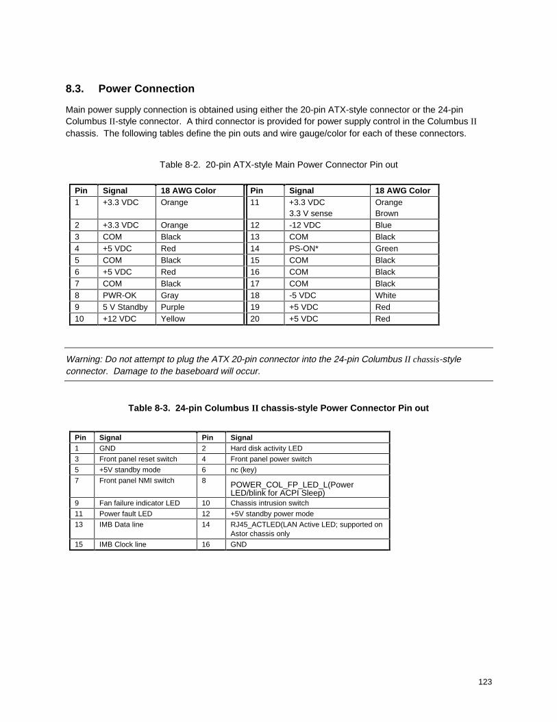
123
8.3. Power Connection
Main power supply connection is obtained using either the 20-pin ATX-style connector or the 24-pinColumbus II-style connector. A third connector is provided for power supply control in the Columbus IIchassis. The following tables define the pin outs and wire gauge/color for each of these connectors.
Table 8-2. 20-pin ATX-style Main Power Connector Pin out
Pin Signal 18 AWG Color Pin Signal 18 AWG Color1 +3.3 VDC Orange 11 +3.3 VDC
3.3 V senseOrangeBrown
2 +3.3 VDC Orange 12 -12 VDC Blue3 COM Black 13 COM Black4 +5 VDC Red 14 PS-ON* Green5 COM Black 15 COM Black6 +5 VDC Red 16 COM Black7 COM Black 17 COM Black8 PWR-OK Gray 18 -5 VDC White9 5 V Standby Purple 19 +5 VDC Red10 +12 VDC Yellow 20 +5 VDC Red
Warning: Do not attempt to plug the ATX 20-pin connector into the 24-pin Columbus II chassis-styleconnector. Damage to the baseboard will occur.
Table 8-3. 24-pin Columbus II chassis-style Power Connector Pin out
Pin Signal Pin Signal1 GND 2 Hard disk activity LED
3 Front panel reset switch 4 Front panel power switch
5 +5V standby mode 6 nc (key)
7 Front panel NMI switch 8 POWER_COL_FP_LED_L(PowerLED/blink for ACPI Sleep)
9 Fan failure indicator LED 10 Chassis intrusion switch
11 Power fault LED 12 +5V standby power mode
13 IMB Data line 14 RJ45_ACTLED(LAN Active LED; supported onAstor chassis only
15 IMB Clock line 16 GND

124
Table 8-4. 14-pin Auxiliary Power Connector Pin out
Pin Signal Pin Signal1 +5V standby power mode
sense Return2 +5V standby power mode
Sense
3 +3V Sense 4 +3V Sense Return
5 IMB Clock line 6 IMB Data line
7 GND 8 POWER_GOOD
9 PS_POWER_ON 10 GND
11 +5V standby power mode 12 nc (Key)
13 Reserved 14 VCC 24
8.4. Power Consumption
The following table shows the power consumed on each supply line for a N440BX Server baseboard with2 processors, 4 DIMMs, 4 PCI slot loads (2A @ 5V per slot), and 1 ISA slot load (Server Monitor Moduleboard).
NOTE:
The following numbers are provided as an example. Actual power consumption will vary depending on theexact N440BX Server configuration. Refer to the appropriate system chassis document for moreinformation.
Table 8-5. Power Consumption
Device(s) 3.3V +5V +12V -12V 5VStandby
Processors 3.04A 8.17A 3.41AMemory DIMMs 3.58AGTL Termination 2.91ANBX 1.20ABaseboard .32A 2.56A .2A .15A .8AFans 1.0AKeyboard/Mouse .5APCI slots 8AISA slot .1A 1.0ATotal Current 11.05 A 19.33 A 5.61 .15A .8A TotalTotal Power 36.47 W 96.65 W 67.32W 1.8W .4W 202.74W
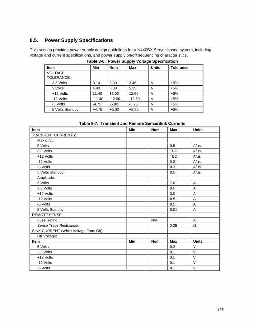
125
8.5. Power Supply Specifications
This section provides power supply design guidelines for a N440BX Server-based system, includingvoltage and current specifications, and power supply on/off sequencing characteristics.
Table 8-6. Power Supply Voltage Specification
Item Min Nom Max Units ToleranceVOLTAGETOLERANCE: 3.3 Volts 3.14 3.30 3.46 V +5% 5 Volts 4.80 5.00 5.25 V +5% +12 Volts 11.40 12.00 12.60 V +5% -12 Volts -11.40 -12.00 -12.60 V +5% -5 Volts -4.75 -5.00 -5.25 V +5% 5 Volts Standby +4.75 +5.00 +5.25 V +5%
Table 8-7. Transient and Remote Sense/Sink Currents
Item Min Nom Max UnitsTRANSIENT CURRENTS: Max dI/dt: 5 Volts 0.5 A/µs 3.3 Volts TBD A/µs +12 Volts TBD A/µs -12 Volts 0.3 A/µs -5 Volts 0.3 A/µs 5 Volts Standby 0.5 A/µs Amplitude: 5 Volts 7.0 A 3.3 Volts 0.5 A +12 Volts 3.0 A -12 Volts 0.5 A -5 Volts 0.5 A 5 Volts Standby 0.01 AREMOTE SENSE: Fuse Rating: N/A A Sense Trace Resistance: 0.05 ΩSINK CURRENT (While Voltage Form Off): Off Voltage:Item Min Nom Max Units 5 Volts 0.2 V 3.3 Volts 0.1 V +12 Volts 0.1 V -12 Volts 0.1 V -5 Volts 0.1 V
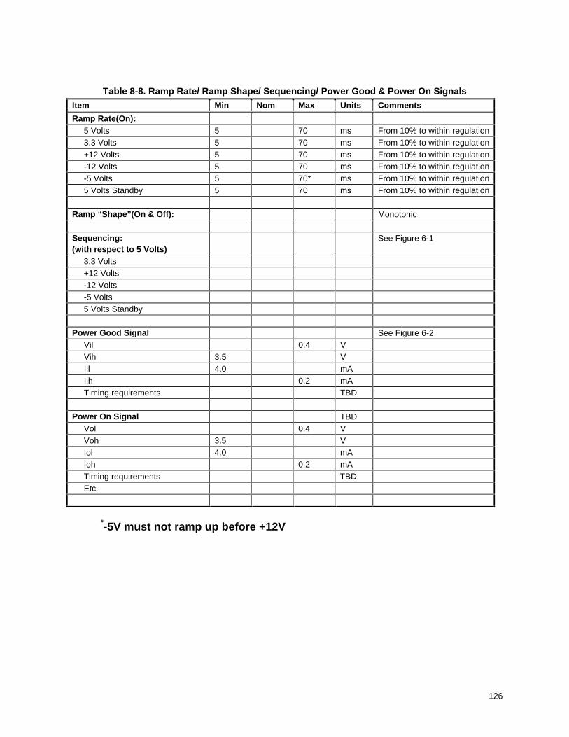
126
Table 8-8. Ramp Rate/ Ramp Shape/ Sequencing/ Power Good & Power On Signals
Item Min Nom Max Units Comments
Ramp Rate(On): 5 Volts 5 70 ms From 10% to within regulation 3.3 Volts 5 70 ms From 10% to within regulation +12 Volts 5 70 ms From 10% to within regulation -12 Volts 5 70 ms From 10% to within regulation -5 Volts 5 70* ms From 10% to within regulation 5 Volts Standby 5 70 ms From 10% to within regulation
Ramp “Shape”(On & Off): Monotonic
Sequencing:(with respect to 5 Volts)
See Figure 6-1
3.3 Volts +12 Volts -12 Volts -5 Volts 5 Volts Standby
Power Good Signal See Figure 6-2 Vil 0.4 V Vih 3.5 V Iil 4.0 mA Iih 0.2 mA Timing requirements TBD
Power On Signal TBD Vol 0.4 V Voh 3.5 V Iol 4.0 mA Ioh 0.2 mA Timing requirements TBD Etc.
*-5V must not ramp up before +12V
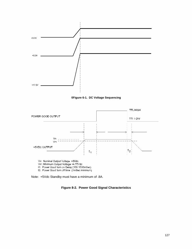
127
0 Figure 6-1. DC Voltage Sequencing
Note: +5Vdc Standby must have a minimum of .8A.
Figure 8-2. Power Good Signal Characteristics
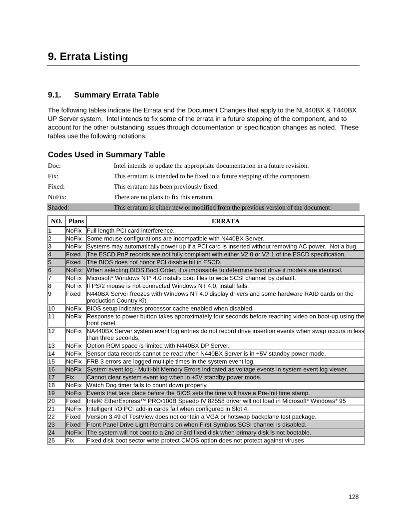
128
9. Errata Listing
9.1. Summary Errata Table
The following tables indicate the Errata and the Document Changes that apply to the NL440BX & T440BXUP Server system. Intel intends to fix some of the errata in a future stepping of the component, and toaccount for the other outstanding issues through documentation or specification changes as noted. Thesetables use the following notations:
Codes Used in Summary TableDoc: Intel intends to update the appropriate documentation in a future revision.
Fix: This erratum is intended to be fixed in a future stepping of the component.
Fixed: This erratum has been previously fixed.
NoFix: There are no plans to fix this erratum.
Shaded: This erratum is either new or modified from the previous version of the document.
NO. Plans ERRATA1 NoFix Full length PCI card interference.2 NoFix Some mouse configurations are incompatible with N440BX Server.3 NoFix Systems may automatically power up if a PCI card is inserted without removing AC power. Not a bug.4 Fixed The ESCD PnP records are not fully compliant with either V2.0 or V2.1 of the ESCD specification.5 Fixed The BIOS does not honor PCI disable bit in ESCD.6 NoFix When selecting BIOS Boot Order, it is impossible to determine boot drive if models are identical.7 NoFix Microsoft* Windows NT* 4.0 installs boot files to wide SCSI channel by default.8 NoFix If PS/2 mouse is not connected Windows NT 4.0, install fails.9 Fixed N440BX Server freezes with Windows NT 4.0 display drivers and some hardware RAID cards on the
production Country Kit.10 NoFix BIOS setup indicates processor cache enabled when disabled.11 NoFix Response to power button takes approximately four seconds before reaching video on boot-up using the
front panel.12 NoFix NA440BX Server system event log entries do not record drive insertion events when swap occurs in less
than three seconds.13 NoFix Option ROM space is limited with N440BX DP Server.14 NoFix Sensor data records cannot be read when N440BX Server is in +5V standby power mode.15 NoFix FRB 3 errors are logged multiple times in the system event log.16 NoFix System event log - Multi-bit Memory Errors indicated as voltage events in system event log viewer.17 Fix Cannot clear system event log when in +5V standby power mode.18 NoFix Watch Dog timer fails to count down properly.19 NoFix Events that take place before the BIOS sets the time will have a Pre-Init time stamp.20 Fixed Intel® EtherExpress™ PRO/100B Speedo IV 82558 driver will not load in Microsoft* Windows* 9521 NoFix Intelligent I/O PCI add-in cards fail when configured in Slot 4.22 Fixed Version 3.49 of TestView does not contain a VGA or hotswap backplane test package.23 Fixed Front Panel Drive Light Remains on when First Symbios SCSI channel is disabled.24 NoFix The system will not boot to a 2nd or 3rd fixed disk when primary disk is not bootable.25 Fix Fixed disk boot sector write protect CMOS option does not protect against viruses
129
9.2. ERRATA
1. Full length PCI card interference
PROBLEM: If there is a cable in the narrow SCSI connector, some full-length PCI add-in cards that areinstalled into the slot closest to processors (PCI 4) will not seat fully. The bracket hinders the add-in cardfrom seating fully.
IMPLICATION: The user will be restricted from using some full-length add-in cards in PCI slot 4.
WORKAROUND: None identified.
STATUS: NoFix.
2. Some mouse configurations are incompatible with the N440BX DP Server
PROBLEM: The N440BX baseboard will not recognize some PS/2 mouse configurations. Specifically whena PS/2 mouse is attached to a 25’ extension, the mouse often fails to be recognized by most operatingsystems. When using a switch box the user is limited to an extension cable that is no longer than 6’.
IMPLICATION: With certain operating systems, when using a long mouse extension cable the mouse will notbe recognized and not be functional.
WORKAROUND: None identified.
STATUS: NoFix.
3. Systems may automatically power up if a PCI card is inserted without removing AC power.Not a bug.
PROBLEM: If the system has been powered down via the front panel power switch, some devices are still ina powered up mode due to the N440BX’s system management features.
IMPLICATION: Inserting a card in the PCI slots without unplugging the system may short some PCI pinstogether, causing the PCI_PME_L signal to bring the system into a fully powered mode. Due to thehazard this poses we recommend users unplug the system before opening the system.
The following is called out in our user guide documentation:
WARNINGSSystem power on/off: The DC push-button on/off switch (a convex button) on the front panelDOES NOT turn off the system AC power. To remove power from system, you must unplug the ACpower cord from the wall outlet.
WORKAROUND: None
STATUS: NoFix.
130
4. The Extended System Configuration Data (ESCD) Plug-n-Play records are not fullycompliant with either V2.0 or V2.1 of the ESCD specification
PROBLEM: The Plug-n-Play ESCD records indicate compliance with v2.0 of the ESCD specification.
IMPLICATION: The Plug-n-Play ESCD records are not completely compliant with either v2.0 or v2.1 of thePlug-n-Play specification.
WORKAROUND: None identified.
STATUS: Fixed. All records have been updated to V2.1 of the ESCD spec in BIOS 9 and newer.
5. BIOS does not honor PCI disable bit in Extended System Configuration Data (ESCD)
PROBLEM: The ESCD free-form record for PCI devices contains a field that indicates if a PCI functionshould be enabled or disabled. The Server Setup Utility (SSU) will set this bit if the user requests todisable a PCI device. On the next boot, the BIOS should turn off the command register in the PCI device,ignore its option ROM, and ignore any resource requirements found in the function’s Base AddressRegisters or Interrupt Pin.
IMPLICATION: If the onboard devices are disabled through the SSU, their resources will be reallocated on thenext system boot.
WORKAROUND: None
STATUS: Fixed. This issue is resolved with SSU3 and BIOS release 9 or newer.
6. When selecting BIOS boot order it is impossible to determine the boot drive if models areidentical
PROBLEM: Using identical drives, it is impossible to determine which drive corresponds to which logical unitnumber (LUN).
IMPLICATION: If two identical drives are installed, the user will not be able to determine which drivecorresponds to which LUN in BIOS setup.
WORKAROUND: None identified.
STATUS: Fix - in a future SCSI BIOS revision.
7. Microsoft* Windows NT* 4.0 installs boot files to the wide SCSI channel by default
PROBLEM: Microsoft Windows NT always installs its boot loader files to the first hard drive it finds in thescan order of the SCSI controller regardless of BIOS configuration. The scan order of the Symbios SCSIcontrollers are wide (hba 0) then narrow (hba 1) channels.
IMPLICATION: To install Microsoft Windows NT to a Narrow SCSI drive while a wide SCSI drive is present,Microsoft Windows NT will place the boot files on hba 0, id=0, which is the drive connected to the widecontroller and the rest of the install on the narrow device.
WORKAROUND: In the Symbios configuration utility, change the default boot order from dev 68 = 0, dev 69 =1 to dev 69 = 0, dev 68 = 1.
STATUS: NoFix.

131
8. If PS/2 mouse is not connected, Microsoft* Windows NT* 4.0 install fails
PROBLEM: When the Microsoft Windows NT 4.0 install process tries to load the kernel and drivers it hangsafter displaying OS version and kernel type if the PS/2 mouse is not connected.
IMPLICATION: Microsoft Windows NT 4.0 cannot install without a pointing device on a N440BX DP Server.
WORKAROUND: None identified.
STATUS: NoFix.
9. Microsoft* Windows NT* 4.0 freezes with production Country Kit video drivers and somehardware RAID cards
PROBLEM: Microsoft Windows NT 4.0 freezes and produces an “orange” or “blank” screen when usingsome hardware RAID solutions and production Country Kit display drivers.
IMPLICATION: The N440BX Server system must boot with the standard VGA option displayed on the NT Bootloader.
WORKAROUND:
STATUS: Fixed-- Version 1.22 of the Cirrus 5480 display drivers for Microsoft Windows NT 4.0 available atthe Intel web site www.intel.com/support.
10. BIOS setup reports processor cache enabled when disabled
PROBLEM: The Pentium® II processor algorithm dictates that the processor cache is disabled if processorspeed is less than 3 times the front side bus speed. This occurs when the CMOS is cleared and the userimmediately enters BIOS setup before setting the CMOS clear jumper back to normal operation. BIOSsetup will indicate that the cache is enabled when it is really disabled.
IMPLICATION: Cache is disabled despite setup reporting that it is enabled during CMOS clear.
WORKAROUND: Setting the clear CMOS jumper back to normal will set the default processor speed to 3times the front side bus speed and enable the cache.
STATUS: NoFix.
11. Response to power button takes approximately four seconds before video display occurson boot-up
PROBLEM: If the N440BX is turned off using the front panel switch before video is reached during POSTthere will be a four second delay in the system shutting down.
IMPLICATION: The PIIX4 does not get initialized until POST 52 (video). If the power button is depressedbefore this time the baseboard management controller (BMC) senses the change in state and will wait fora message from the PIIX4 until its time-out period has reached about four seconds. If there is nomessage, the BMC will then force the system to power down.
WORKAROUND: None identified.
STATUS: NoFix - this is normal operation.

132
12. N440BX Server system event log entries do not record drive insertion events when driveswap occurs in less than three seconds
PROBLEM: In an Astor chassis hot-swap drive bay, insertion events will not be logged if the drive is removedand reinserted in a time span of less than three seconds.
IMPLICATION: The drive may not get an ID or power and will not function correctly.
WORKAROUND: Wait more than 3 seconds before inserting a drive after removing a drive.
STATUS: NoFix.
13. Option ROM space limited on the N440BX DP Server
PROBLEM: When configuring a N440BX with multiple add-in cards using option ROMs, the system mayhang or skip an option ROM while scanning, if there is not enough space to load all ROMs.
IMPLICATION: Every device requires a certain amount of option ROM space to function. The N440BX hasc800 to e000h available for high memory. However, certain configurations will not fit inside of this spacecausing the system to hang or leave out one or more add-in cards.
WORKAROUND: None identified at this time.
STATUS: NoFix.
14. Sensor data records cannot be read when server is in +5V standby power mode
PROBLEM: With the power off and the N440BX Server system in +5V standby power mode, the sensor datarecords cannot be read using the emergency management console or server management software.
IMPLICATION: When querying the baseboard management controller for sensor data records, no error isgiven and zero SDR records are reported even when SDR records are present.
WORKAROUND: None identified at this time.
STATUS: NoFix.
15. FRB3 errors are logged multiple times in the system event log
PROBLEM: Once the baseboard management controller has marked a processor as having a FRB 3 error, it is logged into thesystem event log on every boot. The FRB 3 error should only be logged on the first boot-up. This causes the error to appear as ifan FRB 3 error is occurring on each and every boot, this is not the case.
IMPLICATION: The number of errors in the system event log is artificially inflated.
WORKAROUND: In order to clear the FRB 3 error enter BIOS setup and enable Processor Retest Option.
STATUS: NoFix.
16. Multi-bit memory errors indicated as voltage events in system event log viewer
PROBLEM: A multi-bit memory error is misreported as a voltage event in the system event log.
IMPLICATION: By injecting many multi-bit memory errors while the BIOS is trying to service the original error avoltage event is entered into the system event log. The BIOS handles the event normally and writes theevent out to the BMC when it gets a single occurrence of a multi-bit memory error. The event is reportedcorrectly.
WORKAROUND: None identified at this time.
STATUS: NOFix – This is normal operation.

133
17. Cannot clear the system event log in +5V standby power mode
PROBLEM: In +5V standby power mode with the baseboard management controller and system event logbuffer either full or partially filled, a user can issue the “clear system event log” command. It will appear toexecute normally but a “Get System Event Log” information command indicates the same system eventlog entry count reported just before the clear. Powering the BMC up completely (booting the system) andre-sending the “Get System Event Log” command will indicate that the only two events were power downand power up.
IMPLICATION: It will be necessary to power the system up and re-issue the “Get System Event Log”command to get the accurate system event log entry count after clearing the event log.
WORKAROUND: None identified at this time.
STATUS: Fix.
18. Watch Dog Timer failing to count down properly
PROBLEM: If the count down value is set to 12h or below, the timer counts down to zero very rapidly orinstantaneously. On rare occasions it will count properly and count down to 08h in second intervals.
IMPLICATION: Processor test will fail and system will halt.
WORKAROUND: If the timer is set to 15h which is equivalent to 2 seconds it reliably counts down to 0 in 1second intervals.
STATUS: NoFix.
19. Timing issues when N440BX Server system is in +5V stand-by power mode
PROBLEM: When the server is in +5V stand by power mode, the system event log and sensor data recordstime is zero. If the time is reset, it does not begin to increment while in +5V stand-by power mode.
IMPLICATION: Events that take place before the BIOS sets the time will have a Pre-Init time stamp.
WORKAROUND: None identified at this time.
STATUS: NOFix.
20. Intel EtherExpress™ PRO/100B 82558 driver will not load in Microsoft* Windows* 95
PROBLEM: The driver for the integrated 82558 network component on the N440BX DP Server baseboardwill not load in Windows 95.
IMPLICATION: The integrated network component is inoperable upon installation of this driver.
WORKAROUND:
STATUS: Fixed. Enable PnP OS in the BIOS setup. Install Windows 95 with, or without, network support. InControl Panel, System, remove the network adapter under other bus, under PCI. Reboot the system, afterwhich the system will find the NIC and request the driver. Insert the 2.0 82558 driver and choose the82558 integrated controller with wired for management (wfm) support. Insert the Windows 95 CD andreboot. The network is now installed and it is possible to load other network support packages, such asTCP/IP.
134
21. PCI add-in card failure when configured in Slot 4 of the N440BX DP Server
PROBLEM: PCI add-in cards designed with the Intel i960® or Intelligent I/O cards may fail on the N440BXDP Server when configured in Slot 4 of the baseboard as a result of bus contention.
IMPLICATION: The system may hang if an Intelligent I/O card such as an Intel i960® is used in Slot 4. Thisonly affects slot 4. Slot 4 my be used with any PCI card that does not use more than 1 interrupt line.
WORKAROUND: NONE
STATUS: NoFix:
22. Intel™ TestView Version 3.49 does not contain a VGA or hotswap backplane test package
PROBLEM: Cannot test the VGA or hotswap backplane with TestView V3.49
IMPLICATION:
WORKAROUND:
STATUS: Fixed. Update to the latest version of TestView. Version 4.03S.
23. Front Panel Drive Light Remains on when First Symbios SCSI channel is disabled.
PROBLEM: When the first Symbios channel is disabled and there are no devices attached, the hard driveactivity light remains on after booting to the operating system.
IMPLICATION: HD indicator light is inaccurate.
WORKAROUND: This is fixed by installing the current Symbios driver under the operating system. This doesnot correct the activity light between the scan of the SCSI bus in POST to the point in which the operatingsystem loads the driver.
STATUS: Fix.
135
24. The system will not boot to a 2nd or 3rd fixed disk when primary disk is not bootable.
PROBLEM: The N440BX will not boot to a drive that has a lower boot priority than a non-bootable drive thathas #1 priority, as set in CMOS setup.
IMPLICATION: Explanation:
Each hard drive in the system is numbered sequentially in ascending order starting from 80. The numberassigned to the drive is determined by one of the following methods:
1) For non-PnP compliant option ROMs or devices, the scan option ROM execution order determines thedrive number. When the option ROM is invoked, it claims a range of drive numbers corresponding to thenumber of logical drives it possesses (0, 1, or more). Exact drive numbering can not be controlled by theBIOS when using non-PnP compliant option ROMs or devices.
2) For PnP compliant option ROMs or devices, the multi-boot component of the BIOS controls the orderthat drives are assigned by selectively invoking connection vectors in the option ROMs. Calling aconnection vector signals the option ROM to claim a drive number. By controlling the order of theconnection vector execution, the drive numbers may be assigned in a specific order. In general, once adrive number has been claimed/assigned, it can not be reclaimed or reassigned. The boot drive willalways be drive 80 because the OS boot loader specifically requests data from drive 80. Since a drivenumber can not be reassigned if the drive fails to boot and the boot drive must be drive 80, no other harddrive may be booted from. The order of the drives in the multi-boot menus will determine how drivesattached to the PnP-compliant option ROMs will be numbered.
WORKAROUND: None.
STATUS: NOFix – This is normal operation.
25. Fixed disk boot sector write protect CMOS option does not protect against viruses.
PROBLEM: BIOS Setup option "Fixed Disk Drive Boot Sector- Write Protect" does not prevent viruses fromwriting to the master boot record MBR.
IMPLICATION: The system is susceptible to Virus infections.
WORKAROUND: None
STATUS: Fix.