Embed Size (px)
Citation preview

Enhancing Secure Elements - Technology and Architecture
Bertrand Cambou, Northern Arizona University ABSTRACT: Current secure elements that are mainly flash based operate at
high power, slow access time, and they are vulnerable to side channel attacks. We are suggesting to replace flash with ReRAMs that are faster and operate at much lower power. We are proposing the integration within the secure memory of cryp-tographic primitives such as Physically Unclonable Functions (PUFs), and Ran-dom Number Generators (RNG). Ternary logic, and Machine Learning architec-tures brought to secure elements enable the design of strong PUFs and RNGs.
INTRODUCTION: In the last 20 years secure microcontrollers were success-
fully implemented to create a new class of devices, the smartcards, which have been widely popular to secure hand held terminals in the form factor of SIM cards (Subscriber Identification Module), banking cards, and access cards (ID and transport). About 8 billion of these components are manufactured annually to ful-fill the demand. Initially these microcontrollers were manufactured with embed-ded EEPROM which is now often replaced by Flash to reduce costs. Secure mi-croprocessors, also called “Secure Elements”, are in the process of being widely deployed to enhance hardware security of cyber physical systems (CPS), Internet of Things (IoT), Automotive, smart grid, and many other sensitive systems. Public Key Infrastructure (PKI), an architecture which rely on private cryptographic keys that are kept secret, has been accepted as a way to authenticate users. The success in the adoption of Secure Elements was based on their capability to precisely store these private cryptographic keys for PKI; as well as their ability to perform power-ful cryptographic computations such as encryption, decryption and authentication. The efforts to further enhance secure elements through new Nano-technologies and novel architectures are of strategic importance to reduce cyber-crimes, and to develop a new economy based on trustworthy secure e-commerce.
12.1 GENERAL DESCRIPTION Secure elements [1-5] contain integrated microcontrollers with 32 to 64 bit
RISC engine, a crypto-processor with capability to perform encryption/decryption algorithms such as RSA, ECC, AES, and DES. About 10 to 30Kbyte of SRAM are usually embedded within the CPU and the crypto-processor. The embedded non-volatile memories have a capacity of 100KByte to 1MByte and are driven by a secure memory management unit (MMU). The architecture also includes periph-eral interfaces, analog and glue logic, power management and internal clock gen-erators. A simplified block diagram is described in Fig. 1. International standards such as ISO/IEC 7816 specify contact based smart cards, while ISO/IEC 14443 or 18092 specify contactless identification cards. The Global Platform alliance has successfully driven a standardization of the operating systems (OS) along Java-

2
card and Multos. This has allowed the development of third party value added ap-plications, or Applets, cryptographic methods, deployment of the public key infra-structure (PKI), and client management systems (CMS). Embedded secure ele-ments (eSE) are directly integrated within the final devices, such as a mobile phone. “eSE” does not require the same level of standardization as smart cards, and costs can be reduced by eliminating the micro-module and separate connect-ors. In wireless applications the business model of eSEs is different than SIM cards, e.g. they are not removable from the phone, so a user cannot change carrier or phone while keeping its SIM card.
12.1.1 Encryption and PKI deployment Cryptography is an important technology for SEs, we are summarizing some
elements as background information for this chapter, [6-7]. If P is the plain text that need to be encrypted, K S the symmetrical key, and E is the encryption algo-rithm, the cypher C is given by the equation (1), and can be decrypted with algo-rithm D and the same key:
C = E (P, K S ) (1) P = D (C, K S ) (2)
The Data Encryption Standard (DES) algorithm based on 56 bit keys, devel-oped by IBM and the US government in the 70’s, is inadequate for high security applications. It has been replaced frequently after 2000 by the Advanced Encryp-tion Standard (AES) algorithm that is based on 128 bit keys or larger, as devel-oped by Joan Daemen and Vincent Rijmen; AES is also called the Rijndael code. Both DES and AES algorithms are usually ported into secure elements to perform basic encryption/decryption function. Symmetrical encryption methods are very effective and play an important role in hardware authentication. However these methods are not appropriate to handle large groups of users. The invention of asymmetrical cryptography in the 70’s has been widely adopted for this purpose to secure CPS, mobile and fixed users, access control, and IoT. Each user (i) has two unique cryptographic keys, a public key K PU-i that is shared with other users, and

3
a private key K PR-i that is kept secret [Note: in the case of IoT, and secure ele-ments, both private and public keys are kept secret]. These two keys have a level of symmetry with each other: It is possible to encrypt with one key, public or pri-vate, and to decrypt the result with the other key. Two cyphers C1 and C2 can be created from these two keys following the equations:
C1 = E (P, K PU-i ) ; P = D (C1, K PR-i ) (3) C2 = E (P, K PR-i ) ; P = D (C2, K PU-i ) (4) The method allows two users (i) and (j) to communicate with each other after
exchanging their public keys; the user (i) can send the cypher Ci to user (j) who can decrypt it to retrieve P:
Ci = E [E (P, K PR-i ), K PU-j ] (5) P = D [D (Ci, K PR-j ), K PU-i ] (6) In this double encryption method users (i) and (j) keep their private key secret
from each other. This can offer multiple benefit to the communication: Electronic (digital) signature of user (i). User (j) knows that the message
originate from (i) because it is assumed that only (i) possess the private key K PR-i . So, E (P, K PR-i ) can be considered as an electronic signature.
Protection of the user (j). The only way to decrypt Ci is to possess the pri-vate key K PR-j that is kept secret by user (j).
Non repudiation. To seal the transaction user (j) has to send back to user (i) an encrypted digital signature.
The commercial deployment of asymmetrical cryptography is called public key infrastructure, (PKI). Secure elements were instrumental in the deployment of PKI to enhance access control. In the late 70’s Ronald Rivest, Adi Shamir and Leonard Adleman developed a beautiful algorithm carrying their name, RSA [7], that pro-vides an effective asymmetrical encryption and decryption method. The method exploits the number theory, and in particular the Euler-Fermat theorem; the private and public keys are inverse modulo numbers. To this date the algorithm has been proven as un-breakable; powerful quantum computers might challenge this state-ment in the future. RSA tends to be highly computing intensive, and several orders of magnitude slower than AES. This is no longer a limitation as the compute pow-er of secure elements is now appropriate. Alternate asymmetrical algorithm such as those based on elliptic curves (ECC) are much lighter than RSA, and are widely deployed on the cost sensitive versions of secure elements. In order to strengthen both symmetrical and asymmetrical cryptography it is important to add functions H based on random numbers generators (RNG) to the plain texts P. For example Eq. (1) and Eq. (2) can be written the following way:
C = E (P+H, K S ) (7) P+H = D (C, K S ) (8) In this example both P and H are described by a binary stream of data, and P
length is known by the receiving party. P+H is much longer and complicated to decrypt than P to prevent third party attack. Secure elements need to have a high quality RNG integrated into the component to encrypt important information.

4
What to remember: Secure elements are an essential part of the effective de-
ployment of PKI. They act like vaults hiding cryptographic keys, the private keys for RSA or ECC, and the symmetrical AES keys. Secure embedded non-volatile memories (NVMs) that store these keys are therefore critical. The crypto-processors that decrypt and encrypt messages need access to strong RNGs.
12.1.2 Multi-function authentication In asset, and people protection there is a major difference between “identifica-
tion” and “authentication. “Identification” does not have to be secret as long as they are clear, unique, and unambiguous. “Authentication” is a way to prove that the person or the object is the right one. Authentication factors have to be abso-lutely secret, however they do not have to be unique as long as they can offer a high level of certainty of a match between the person or object involved in the transaction and the ones expected. For example a nice picture with a first and last name are good identification factors, but are not secret and cannot be authentica-tion factors; pin codes are not unique, and cannot be an identification factor, how-ever can be an acceptable authentication factor when kept confidential. In most e-transactions the subject has to provide its ID number as well as the secret pass-word for authentication. The authentication factors are the first line of defense to prevent hackers from breaking a system. Both identification and authentication factors are stored permanently in secure elements, the users have to provide fresh authentication factors when they wish to access a service. The full authentication cycles are done within the secure elements to enhance secrecy [8, 9].
Authentication factors include pin codes, passwords, biometric prints such as finger print, iris, blood vessels in the fingers, facial features, and voice, as well as hardware prints such as PUFs that exploit micro variations occurring during inte-grated circuit fabrication. The use of multiple factors, also referred to as multi-function (or multi-factor) authentication is expected to be stronger than a single authentication that is based on only one factor. Trustworthy authentications incor-porate cryptography to increase the secrecy of system.
Authentication methods have to reduce both the false rejection rates (FRR) re-
sulting in false negative authentication, and the false acceptance rates (FAR) re-sulting in false positive authentications, see Table 1. False negatives are frequent with biometry considering that human based prints are not constant. Fingerprint authentication frequently face high FRR. Error correction is shown to reduce FRR [10, 11]. However, may also correct hostile messages thereby increasing FAR.

5
What to remember: SEs are utilized to provide reliable multi-function authen-
tication for access control. The metrics to quantify the quality of the authentica-tions are FRR for false negatives, and FAR for false positives.
12.1.3 Embedded secure memories – utilization of Flash Embedded memories of secure elements (SE) have to store client related data-
bases, all cryptographic and authentication keys, the operating systems, and act as cache memory for the processor. The size of the embedded memories vary from a few k-bits for ID and RFID applications to the M-byte level for high end applica-tions. At low densities EEPROM is the preferred technology due to its excellent array efficiency. For low power and low density applications ferroelectric memo-ries, FeRAMs, secured a niche market, and have the potential to expand. The dominant technology for SEs remains embedded flash [12-13], this is due to its low cost at high density, and ability to shrink to the 32nm lithographic node. NOR has been the architecture of choice for embedded flash, however embedded NAND was also successfully introduced to reduce the size of the arrays. A cross section of a flash cell is presented Fig. 2.
The basic principle of flash is the modulation of the threshold voltage of the
metal-oxide-semiconductor (MOS) transistor by selectively trapping electrons in a floating/trapping gate (TG). “1s” are programmed by injecting electrons in the TG, thereby increasing the threshold voltage of the transistor. In NOR flash the electrons are injected through the thin dielectric, also called tunnel, using channel hot electrons (CHE). The energy to “heat” the electrons is added by applying at least 3.5Volt between source and drain, the injection occurs near the drain. In NAND flash the electrons are directly injected by Fowler Nordheim (FN) effect through the tunnel oxide. If ΔV is the voltage differential across the tunnel dielec-tric, Tox its thickness, A and B are physical parameters, the current J circulating through the dielectric is:
J = A (∆𝑽𝑽𝑻𝑻𝑻𝑻𝑻𝑻
)2 𝒆𝒆−𝑩𝑩/( ∆𝑽𝑽𝑻𝑻𝑻𝑻𝑻𝑻
) (9)
The tunnel dielectric has to be thick enough, above 5nm, to retain information and prevent charge losses, so the voltage V BG necessary to program a NAND flash
6
cell has to be large enough, usually greater than 15V. Both CHE and FN requires high voltage transistors that are expensive to integrate with high density logic. The programming cycles are done step by step to avoid over programming condi-tions. Multi-bits per cell are commonly obtained by modulating the electrostatic charges in the TG, thereby creating multiple levels of threshold voltage. For 2-bits per cell, 4 levels are needed, for 4-bits per cell, 16 levels are needed. Traditional Flash cells use floating polysilicon gate to trap these electrons. There is a growing interest to replace the polysilicon with silicon rich silicon nitride TG to reduce the thickness of the structure, and cell to cell electrostatic interactions for high density flash memories. Mirrorbit technology can get 2-bits per cell by trapping charges in a non-conductive nitride TG, one bit near the source, the other one near the drain.
The read cycles are based on sensing the source drain currents that are different for “0”s and “1”s. During erase cycles the negative charges are removed from the trapping gate by FN effect to return to the original threshold voltage. Typically embedded flash memories have an endurance of 100,000 program-erase cycles.
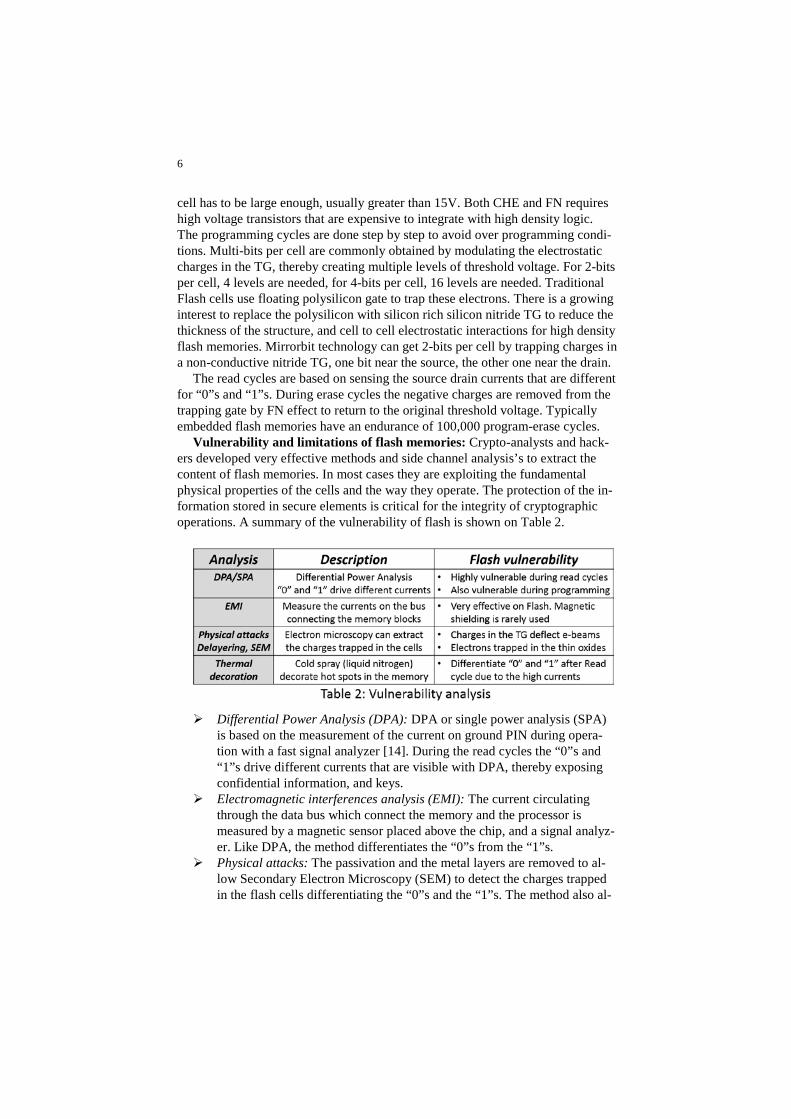
Vulnerability and limitations of flash memories: Crypto-analysts and hack-ers developed very effective methods and side channel analysis’s to extract the content of flash memories. In most cases they are exploiting the fundamental physical properties of the cells and the way they operate. The protection of the in-formation stored in secure elements is critical for the integrity of cryptographic operations. A summary of the vulnerability of flash is shown on Table 2.
Differential Power Analysis (DPA): DPA or single power analysis (SPA)
is based on the measurement of the current on ground PIN during opera-tion with a fast signal analyzer [14]. During the read cycles the “0”s and “1”s drive different currents that are visible with DPA, thereby exposing confidential information, and keys.
Electromagnetic interferences analysis (EMI): The current circulating through the data bus which connect the memory and the processor is measured by a magnetic sensor placed above the chip, and a signal analyz-er. Like DPA, the method differentiates the “0”s from the “1”s.
Physical attacks: The passivation and the metal layers are removed to al-low Secondary Electron Microscopy (SEM) to detect the charges trapped in the flash cells differentiating the “0”s and the “1”s. The method also al-

7
lows the detection of the number of program-erase cycles which leave be-hind charges trapped within the tunnel dielectric.
Thermal decoration: Liquid nitrogen allows the deposition of ice on the chip. The hot spots where electric current circulate melt and decorate the ice. The high power flash technology is vulnerable to these attacks.
Flash memory has also the following limitations for secure elements: High voltage, high power: The programming-erase cycles of flash devices
need high operating voltages (10 to 18 volts). This is challenging for appli-cations, such as RFID, that are power sensitive.
Slow operation: Flash is about 5X slower to read than other memories, and orders of magnitude slower to program. This could open opportunities for the crypto-analyst due to the slowness the crypto-processor.
Complex manufacturing: About 10 additional masking levels are needed to manufacture embedded flash products above and beyond of the basic CMOS flow. It is doubtful that embedded flash will be the preferred solu-tion for secure processors below the 28nm node. Candidate technologies to replace flash in the embedded space include ReRAM, and MRAM. The usage these technologies for SEs is covered in the following sections.
What to remember: Embedded flash is currently the mainstream technology
for mid to high end secure elements. However crypto-analyst are now armed with effective methods to extract the confidential information stored in flash memories.
12.2 USAGE OF ADVANCED MEMORY TECHNOLOGIES
12.2.1 Comparison with Resistive RAM, and Magnetic RAM. ReRAM cells [15 - 17] are based on Nano-materials inserted between two
electrodes switching back and forward between Low Resistivity States (LRS) for “0s”, and High Resistivity States (HRS) for “1s”. Nano-materials such as metal

8
oxides behave as solid electrolytes. As it is shown in Fig. 3 the basic principle be-hind ReRAM, and the switch between LRS and HRS, is the reversible formation of highly conductive filaments between the electrodes. These conductive filaments consist of positively charged oxygen vacancies, or metal ions, migrating toward the cathode. The power necessary to operate ReRAM cells is small compared with flash, and the switching times are lower. Current industrial R&D investments in ReRAM are massive, and this technology is expected to play a major role for fu-ture SEs. Unlike flash, ReRAM can be embedded at advanced CMOS nodes with-out adding too much complexity, due to its compatibility with low power and mainstream manufacturing processes.
Magnetic RAM: Like ReRAM cells, [18], MRAM cells can switch back and
forward between the two states HRS and LRS, see Fig. 4.0. The cells consist of two magnetic domains, a fixed reference, and a second domain that can be pro-grammed in two different directions. A tunnel layer usually made of thin Magne-sium or Aluminum Oxides separates the two domains. When the magnetization of the two domains are aligned, the resistivity of the tunnel oxide is low (LRS) due to the giant magnetoresistance effect; when anti-aligned the resistivity is high (HRS). In the example shown in Fig. 4 the domains have vertical magnetization, and the programming method called STT or spin torque transfer is based on the circulation of a current through the structure. Other MRAMs are based on horizontal magnet-ization and the circulation of a separate current to program the cells through mag-netic field. The small ratio HRS/LRS for MRAMs (about 2 for MRAM compared with 100 or more for ReRAM) is hard to master in volume manufacturing.
Back to back comparison: The typical parameters for embedded flash, Re-RAM, and MRAM are compared in Table 3. For each technology there are large variations, depending on the lithography nodes, the suppliers, and the type of structures. Flash data is the most reliable because ReRAM and MRAM are not yet

9
running in volume production. However, it is clear that embedded flash memories are slower and operate at higher power.
Programming: The ReRAM cells can switch back and forward between
the HRS and the LRS with a few volts, μA currents, and below 10ns. In MRAMs both STT, and TAS need relatively high currents during pro-gramming cycles. Flash can run into an over-programming cycle, and needs to be erased before reprogramming. ReRAM and MRAM do not need erase cycles before programming. For all three technologies the num-ber of guaranteed program-erase cycles is greater than 100 thousand cy-cles, with retentions in excess of 10 years.
Read: Unlike flash, both ReRAMs, and MRAMs can be read quickly at constant current, thereby minimizing exposure to side channel attacks. The high HRS/LRS ratio of ReRAM is particularly attractive to minimize read errors. With flash, charges get trapped in the tunnel oxide during program-erase cycles, so the threshold voltages are drifting faster with the cells that are frequently switched from the two states; the cells storing cryptographic keys tend to be re-programmed less often, and could stick out during cryp-to-analysis. At its forefront, it has been claimed that both ReRAM and MRAM can reach read access times of 1ns versus 50ns for flash.
Erase: It is possible to quickly erase ReRAM at low voltage, low current and in a few ns. This feature is important when a real time attack of the SE is detected. With flash, crypto-analysts can clamp down Vcc below 1.5 volt during side channel attacks preventing a defensive erase cycle and freely analyze the device. During the life cycle of SEs it is also required to reprogram some of the cryptographic keys, this is faster with ReRAMS.

10
What to remember: The back to back comparison of flash, ReRAM, and MRAM for SEs is favorable to ReRAM due to its low power and fast access time. Flash benefit from its legacy position for now, and MRAM lacks manufacturabil-ity.
12.2.2 Usage of Content Addressable Memories (CAM) Internet Protocol (IP) routers and high performance microprocessors are cur-
rently using CAM to accelerate the rate of pattern matching per second. Large CAMs contain data bases of IP addresses that are compared at once with one par-ticular IP address, the input pattern. CAM has a parallel architecture that extracts the location in the memory of these matching IP addresses. The comparison of the input pattern with thousands of IP addresses are done “in situ” without ever read-ing the input pattern. At the level of each cell, the stored bits are XORed (XOR is the Boolean instruction ⊕ defined by: 0⊕0=0; 1⊕1=0; 0⊕1=1; 1⊕0=1) with the bits from the input pattern. Each CAM cell typically contains two 6T SRAM cells, one for the stored bits, one for the input bit, and an XOR logic element.
Beside SRAM, there are methods to design a CAM architecture with flash,
ReRAM or MRAM [19-21]. Fig. 5 shows an example of CAM cell design with ReRAM. In this example two pin codes are stored in the ReRAM. During cycle-1 of the authentication, the four XOR engines (C1, C2, C3, C4) compare pin-1 (the stored pattern is 1110) with the input data 0010; then pin-2 0010 is compared dur-ing cycle 2 of the authentication with the same input data, this is the matching pin. In case of a mismatch the parallel architecture will not disclose which bit is a miss. This design, of Fig. 5, can be generalized by increasing the width of the compare elements to words as large as thousand bits rather than 4, and by adding parallel elements to perform multiple compare cycles at once. When embedded within se-cure elements, the CAM architecture can be very effective in performing some important authentication functions such as password check, pin code verification,

11
or PUF challenge response pairs (CRP) matching. This method can resolve a weakness inherent with traditional RAM architecture where password or pin codes are extracted from the memory array for authentication, exposing the information to Crypto-analysts. One of the side channel analysis to extract secret keys is to bring bad keys to the secure element, and to observe the transfer of data between the memory block and the processing element. The ability to directly compare an input key with stored patterns in a CAM eliminates this potential attack. This solu-tion is not applicable for all cryptographic primitives. For example a private key needs to be extracted from the secure memory to decrypt messages encrypted with the public key. It is then desirable to have both a RAM, and a CAM architecture available in the SE to manage the multiple keys and cryptographic primitives: Storage in the embedded RAM: asymmetric keys (RSA, ECC public and
private keys), symmetric keys (DES, AES…), biometric minutia. Storage in the CAM: pin codes, passwords, PUF responses, biometric print.
What to remember: Authentications such as in situ password verification can
benefit from CAM architectures and reduce the exposure to crypto-analysis. RAM architecture is still needed for cryptographic key storage.
12.3 USAGE OF PHYSICALLY UNCLONABLE FUNCTIONS 12.3.1 PUFs within secure elements
PUFs act as virtual fingerprints for the hardware, and can provide unique signa-tures during the authentication processes [22, 33]. The inherent randomness, and uniqueness of the PUF can be derived from the natural variation obtained during the manufacturing of memory blocks. The underlying mechanism of a PUF is to exploit the variation of the physical parameters of the memory cells to generate an initial digital “fingerprint” called a challenge (i.e. input) of typically 128 bits. This challenge is sent to a secure server for reference. The PUF can generate fresh re-sponses (i.e. output), and produce a set of Challenge-Response-Pairs (CRPs) that are matching during positive authentications.
The CRPs have to be reproducible, and easy to recognize during the authentication process with minimization of both FAR and FRR, see Table 1. As shown on Fig.

12
6, 6T SRAM memory arrays are good PUF candidates. Each SRAM cell, when tuned on, has the opportunity to switch as a “0” or a “1”, however due to small manufacturing asymmetries some cells will always prefer one side. As a result a PUF array consisting of multiple SRAM cells can generate reproducible challeng-es and responses. This method has been exploited for commercial authentications. Such PUFs have a number of limitations and lack trustworthiness that could create a false sense of security. One major concern is the exposure to hacker, and their ability to extract un-encrypted PUF responses, which largely defeats the value of the method. There is value to embed the PUF within a secure encrypted elements that can decrypt the challenges coming from the secure server, see section 12.1.1, and thereby perform “in situ” authentication. Below is an example of authentica-tion with secure element: Assumption 1: the SE A generates a PUF challenge C A that was down-
loaded to the server B, it has RSA keys KprA and KpuA, an identification ID A , and an AES key Ks. The PUF generates responses to RAi for each authentication “i”, and hash functions HAi 1 and HAi 2 based on its own RNG.
Assumption 2: the secure server B has the keys KprB, KpuB, and Ks, as well as a data base with the information related to A that includes C A , KpuA, and ID A , and can generate the hash function HBi.
In this example the authentication is done in three steps: Step 1 the SE A send its encrypted identity ID A to the server B; Step 2 B send an encrypted challenge C A to A; Step 3 A perform the CRP matching to authenticate B, if positive A send back to B the certificate ID A +C A :
C1 = E ((E {ID A , Ks}) +HAi 1 , KpuB) (10) C2 = E [E (E {C A , Ks} +HBi), KprB], KpuA] (11) C3 = E [E (E {ID A +CA , Ks} +HAi 2 , KprA), KpuB]
(12) Such an authentication protects for both parties, A identifies B with the PUF,
and B identifies A with its ID and asymmetrical key. The concept of non-repudiation was incorporated in this communication, because both the SE and the server did use their secret private key in the process.
What to remember: Embedding PUFs, which are acting as hardware “finger-
prints”, within secure elements strengthens the authentication processes, and al-lows all communication between the SE and the server to be encrypted.
12.3.2 PUFs with embedded memories In addition to SRAM, PUFs can be generated from DRAM, ReRAM, MRAM,
and flash memories, see Table 4. Each memory technology has physical parame-ters that can be exploited for the design of PUFs. Variations of properties such as lithographic critical dimensions, doping levels of semiconducting layers, resistivi-ty of connecting materials, threshold voltages of MOS transistors, and others [23 - 33] can make each PUF device unique and identifiable from all others when pro-duced by the same manufacturing process.

13
DRAM: In a DRAM, each cell contains a capacitor that is selectively charged to store a “1” (yes) or a “0” (not charged). Subject to natural leak-ages, these cells need to be recharged during the refresh cycles, typically every 1ms. One way to create a PUF is to program an array, then measure the voltage left after a fixed amount of time, for example 2ms. For chal-lenge and response generation, the bottom 50% of the distribution of the cells that leaks the most can arbitrarily be “0”s, while the other half “1”s. This method can be used for stand-alone DRAM, not with existing SEs.
ReRAM: the creation of PUFs out of ReRAM memories is still in a re-search mode. A possible way is to use built-in-self-test (BIST), ref [34] to test a particular parameter in the ReRAM cells of the array, and determine the “0” from the “1”. Three parameters are candidates for PUF, Rmax cor-responding to HRS, Rmin corresponding to LRS, and Vset (see Fig. 3). Rmax exhibits the largest cell to cell variation, while Vset has a tighter distribution. Rmax based PUFs are expected to have the lowest CRP error rates, FAR, and FRR. Vset based PUFs might have higher error rates, however, they are more difficult to extract through side channel analysis because the “0”s and the “1”s can be close to each other.
MRAM: The method to create PUFs with MRAM is similar to that of Re-RAMs. The resistivity of the HRS can be exploited, with a transition be-tween the “0”s and the “1”s, located at the median of the distribution.
Flash: a method to create PUF from flash memories is to exploit the pro-gramming mechanism. As shown in Fig. 2, during flash cell programming electrons are injected to the trapping gate to change the threshold voltage of the MOS transistor. In order to generate PUF challenges and responses, the injection time is fixed, giving each cell the opportunity to have differ-ent threshold voltage; 50% of the cells with the lowest threshold are set as a “0”, the remaining are “1s”.

14
Regardless of the type of memory technology, the unique signatures of the PUFs are derived from their intrinsic manufacturing variations, which occur dur-ing the fabrication process. There is an expected level of mismatches between the distribution of parameter P when the challenges were generated (i.e. the initial “print” that was stored in the secure server), and when the responses are freshly generated (the “print” generated before authentication), see Fig. 7, where parame-ter P is the Vset measured on ReRAM samples manufactured at Virginia Tech. The solid electrolytes of these samples are made of CuOx. The median of the dis-tribution is μ=2.1V with a standard variation σ =+0.54V. When a cell has a Vset below μ, a”0” is generated as a challenge, “1”s are generated when Vset is above μ. The second graph called “next PUF” in Fig. 7 is an example of distribution that has drifted between challenge and response.
The drifts occurs when the PUFs are subject to changes related to temperature,
voltage, EMI, aging, and other environmental factors; the resulting responses are then different than the original challenges. The potentially undesirable conse-quences are weak PUFs with high CRP error rates, and high false rejection rates (FRR). Error correction could reduce CRP errors, however, they could also blindly correct hostile challenges, and increase false acceptances (FAR).
What to remember: PUFs can be generated by most commercial memories,
namely SRAM, DRAM, ReRAM, MRAM, Flash, FeRAM, and EEPROM. During authentications, the PUF responses can drift away from the initial challenges of reference, creating CRP errors as well as generating FRRs and FARs.
12.3.2 Strengthening secure memory based PUFs with ternary states PUFs, in addition to having low FRR and low FAR, should be non-obvious
and unclonable, to prevent a third party from easily extracting the responses. These objectives are somewhat opposite, easy to extract parameters P could fulfil the low CRP error rate but fail the obligation of non-obviousness, and this if they
15
are easy to extract by hackers. Conversely, PUF could be extremely hard to un-cover by crypto-analysis at the cost of being hard to read for challenge/response generation, thereby having high CRP error rates and unacceptable FRRs. In the following two sections we present several methods that are aimed to achieve con-currently these objectives, and analyze their potential based on experimental re-sults.
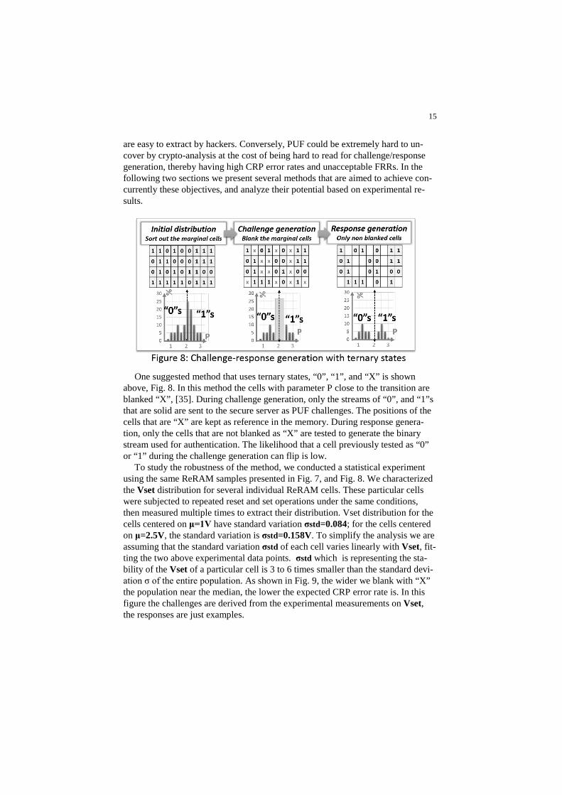
One suggested method that uses ternary states, “0”, “1”, and “X” is shown
above, Fig. 8. In this method the cells with parameter P close to the transition are blanked “X”, [35]. During challenge generation, only the streams of “0”, and “1”s that are solid are sent to the secure server as PUF challenges. The positions of the cells that are “X” are kept as reference in the memory. During response genera-tion, only the cells that are not blanked as “X” are tested to generate the binary stream used for authentication. The likelihood that a cell previously tested as “0” or “1” during the challenge generation can flip is low.
To study the robustness of the method, we conducted a statistical experiment using the same ReRAM samples presented in Fig. 7, and Fig. 8. We characterized the Vset distribution for several individual ReRAM cells. These particular cells were subjected to repeated reset and set operations under the same conditions, then measured multiple times to extract their distribution. Vset distribution for the cells centered on μ=1V have standard variation σstd=0.084; for the cells centered on μ=2.5V, the standard variation is σstd=0.158V. To simplify the analysis we are assuming that the standard variation σstd of each cell varies linearly with Vset, fit-ting the two above experimental data points. σstd which is representing the sta-bility of the Vset of a particular cell is 3 to 6 times smaller than the standard devi-ation σ of the entire population. As shown in Fig. 9, the wider we blank with “X” the population near the median, the lower the expected CRP error rate is. In this figure the challenges are derived from the experimental measurements on Vset, the responses are just examples.

16
In this statistical analysis we studied three cases for challenge generation: 1) blanking +/- 0.27V around the median value of μ=2.1V; 2) blanking +/- 0.54V, and 3) blanking +/- 0.81V. For response generation we are reducing the threshold value to 1.8V to sort out the “0”s from the “1”s. Such a reduction of the threshold reduces the CRP error rates due to the physical asymmetry of the Vset which has lower σstd at lower value. The +/- 0.27V blanking is not large enough, CRP error rates are too high, in the 80,000ppm range. When the blanking is large enough, the likelihood that a bit from a response population can flip from its state as a chal-lenge (“0” to “1” or the opposite) creating a CRP error is negligible: both +/-0.54V and +/-0.81V blanking can yield CRP error rates below 8ppm.
The impact of this error rate on the authentication cycle of a PUF stream of N
bits can be calculated with the Poisson equation. If P(n) is the probability to have n failures over N bits, p is the probability to have one CRP mismatch due to errors, assuming N=128 and p=8ppm (case +/-0.54V). P(n) is given by:
P(n) = λn/n! e-λ (13) λ=pN (14) P(0)=99.2%; P(1)=0.794%; P(2)=0.003%; P(3)≈0. (15) With these results, the probability that at least 126 bits over 128 CRP
candidates are matching during an authentication cycle is almost certain. Such CRP stream error rates are lower than 98% which are much below the generally accepted rate of 90% for PUF authentications. The +/-0.54V blanking correspond to +/- 1σ of the Vset distribution, about 68% of the cells are then blanked “X”, 32% are used for CRP generation. In this example, in order to generate a PUF of 128 bits, the size of the memory array needs to be in the 400 bit range.

17
Non obviousness: The method based on ternary states has potential to enhance the non-obviousness, and unclonability of the PUF for the following reasons: The mapping of the “X”s can be encrypted and stored in the secure
memory. An hacker trying to extract a response would have the difficult task to uncover the location within the memory array used for challenge generation.
The secure element may communicate with the server through binary streams of data, keeping the ternary logic internaly. A hacker would then needs ternary logic to communicate with the PUF within the secure element.
One way to manage ternary states in a secure element is to duplicate the information: manage a (0, 1) pair for a “0”, a (1, 0) pair for a “1”, and a (1, 1) or a (0, 0) for a “X”. Such an internal ternary bit structure can confuse DPA side channel analysis trying to differentiate the “0”s from the “1”s.
There is little need to apply error correction methods in addition of the ternary state method. This can accelerate the authentication process leaving less time for side channel analysis.
Random Number Generators (RNG): As presented section 12.1.1 RNG are important to create hashing functions, and enhance the encryption. RNG that are generated purely by mathematical methods are by definition not really random when a hacker learns to apply the same mathematical method.
As shown in Fig. 10, it is possible to exploit the ternary method presented
above to strengthen the RNG. In this case we want to select only the cells that are close to the threshold between “0”s and “1”s, the “X” states. When subject to one particular reading the stream of binary bits generated by testing the cells with “X” states will have a high level of randomness. For example if the cells with Vset that are +/- 0.1V from the median μ=2.1V are used for RNG, the likelihood that they will flip on the opposite bit after multiple reading is 43%. Let us assume that a random number of 128 bits was generated with half of its bit having a probability p=0.43 to be a “0”, and the other half with p=0.57. Assuming binomial distribu-tion, the likelihood that half of this population is at “0” is not statistically different than a population with p=1 for the first half and p=0 for the second half. Mathe-matical methods to randomly re-order these 128 bits will yield a higher level of

18
randomness when each bit has a probability to flip back and forward close to p=0.5. The usage of a population with p=0.43 is indeed much better than re-ordering a memory array filled with “0”s and “1”s. There are ways to further im-prove this randomness: add noise during the testing of the “0”s and the “1”s, or measuring the Vset at higher sweeping rates.
Implementing ternary states with SE: A first way to implement ternary based PUFs on secure elements is to store the position of the blanked cells “X” some-where in the secure memory. Then, during response generation, the state machine of the memory or memory management unit (MMU) can only exploit non blanked cells. To enhance security the location of the blanked cells can be encrypted.
A second implementation is also based on the use of the memory array as is, while creating ternary states within the array itself. The memory array shall be segmented by pairs of cells to create the ternary states. The first of the two cells, called “active cell” shall be used to generate a PUF challenge, either a “0” or a “1” based on its parameter P. The second cell, called “companion cell”, is to be used to differentiate the state of the active cell: for a state “0”, a “0” is stored in this ac-tive cell, and a “1” is stored on the companion cell. Conversely for a state “1”, a “1” is stored in the active cell, and a “0” in the companion cell. To store a blanked “X” state, the same bit shall be stored both in the active cell, and its companion cell. The MMU will then drive for the SE pairs of bits, (0, 1), (1, 0), and (1, 1) or (0, 0), while the external communication with the server is binary. During authen-tication, the responses are generated by testing only the active cells that were not blanked during the challenge generation, then challenge-response pairs are matched bit by bit. In both implementations there is no need to change the memory array within the SE, only internal logic changes are required.
What to remember: the method to blank the cells susceptible to flip between
0”s and “1”s can reduce CRP error rates in a PUF, and enhance the unclonabil-ity. A “by product” of the method is to strengthen the randomness of RNGs.
12.4 USAGE OF MACHINE LEARNING Machine learning is an architecture that is used in cybersecurity to improve au-
thentication, and detect abnormal behavior of the user, or the server, [36, 39]. On the terminal side, machine learning has been used for biometric authentication to track drifts of the user entries over time. Tara Seal from Info-security Magazine reported in September 2014, that the security company CA Technologies is using machine learning to combat credit card fraud. On the infrastructure side, machine learning has been widely used for computer security, and to protect web authenti-cation. As shown in Fig. 11, Machine Learning Engines (MLEs) can be inserted into secure elements between the server, and the secure memory, to operate in a closed loop, without external intervention to avoid disclosing additional infor-mation during attacks. The MLEs can be then dedicated to the authentication pro-cess. The MLE can be the engine to track behavior of both the user, and the server

19
to flag abnormal situations such as repetitive negative attempts to authenticate, or malicious changes in the power supply. The MLE can also enhance the effective-ness of the PUF, this is the subject of the study presented below.
Track the physical variations of the PUFs with MLE: The PUF responses and challenges are generated the same way with a PUF memory, and this as often as there is need for a fresh authentication, however the responses can vary over-time due to the natural variations of parameter P which underlie the PUF. This can create large CRP errors, and weaken the usefulness of PUFs.
A method to correct such a problem is described below step by step (see Fig. 12). In this method an MLE architecture is combined with a multi-state CRP gen-eration process to track the drift of the responses, and determine if the drift is natu-ral, or has changed due to a malicious entry.
Challenges. As presented section 12.3.2, the PUF Challenges shall be gen-
erated with the memory, “0s” are programmed in the cells where parameter P is below threshold, and a “1” is programmed above the threshold.
Responses. The responses shall be generated with the same method than the challenges. Concurrently the cells shall be organized in 𝒏𝒏 = 𝟖𝟖 multi-ple states i by sorting out the value of parameter P for these cells. For ex-ample, when the response has N=128 bits, the 16 cells with the lowest val-ue are given the state 0, the following 16 cells with the state 1, all the way to the 16 cells with the highest value that are given the state 7. That way the 128 bits of the PUF responses are sorted in 8 different states.
Vector of error – authentication j. Each state 𝒊𝒊 has 𝒏𝒏𝒊𝒊 cells such that ∑ 𝒏𝒏𝒊𝒊−𝟏𝟏𝒊𝒊=𝒏𝒏−𝟏𝟏𝒊𝒊=𝟎𝟎 =N. For a given cell 𝒌𝒌 that is part of the PUF, the CRP error
between the Challenge 𝑪𝑪𝒌𝒌 and the Response 𝑹𝑹𝒌𝒌 is given by the Hamming distance ∆𝑪𝑪𝑹𝑹𝑷𝑷𝒌𝒌 = |𝑹𝑹𝒌𝒌 − 𝑪𝑪𝒌𝒌|. For the state 𝒊𝒊 and its 𝒏𝒏𝒊𝒊 cells, the aver-

20
age CRP error rate E i is given by eq.16. The average error rate E 0 to E n-1 for the 𝒏𝒏 states and the authentication j is giving a Vector of Error VE j , eq.17:
𝑬𝑬𝒊𝒊 = 𝟏𝟏𝒏𝒏𝒊𝒊
∑ |𝑹𝑹𝒌𝒌 − 𝑪𝑪𝒌𝒌| 𝒌𝒌=𝒏𝒏𝒊𝒊𝒌𝒌=𝟏𝟏 (16)
VE j = (𝑬𝑬𝟎𝟎 , 𝑬𝑬𝟏𝟏,., 𝑬𝑬𝒊𝒊 ,. , 𝑬𝑬𝒏𝒏−𝟏𝟏) j (17)
Vector of input – authentication j. The Vectors of Input are resulting from the measurements of environmental parameters surrounding the PUF such as Io temperature, I 1 voltage bias conditions, I i current, and others: I j = (I0 , I1 , .., I i , .., In-1 ) j (18)
Learning data base. Considering that parameter P is a physical parameter, it is possible to develop a predictive model on how the responses are antic-ipated to vary when subject to drifts in the environmental parameters I. This can be used to develop a learning data base which keeps track of VE when parameter P is subject to drifts. The learning database can also con-tain the history of previous authentications, VE h and I h with h<j.
Final authentication j. To produce a “yes” or “no” for authentication j the MLE analyzes the vector of error VE j which contain the average CRP er-ror rates by state together with I j , and the learning data base. This exploits the predictability of parameters P when subject to environmental varia-tions. On the contrary, a challenge brought by a malicious third party when matched with a fresh response would create a VE that is not con-sistent with the learning data base, thereby resulting in a negative authenti-cation.
Experimental validation. In this section we are giving a real example,
based on ReRAM samples produced at Virginia Tech. This should help the reader to better understand the method presented above on how the MLE can analyze CRP errors, and make a determination on authentication j. A summary of the analysis is shown Fig. 13: At room temperature (20 ⁰C) the ReRAM samples produced at Virginia Tech have a Vset median distri-

21
bution μ = 2.1V and standard variation σ = 0.54V. If we assume that both the challenges, and the responses are generated at 20 ⁰C, and the CRP er-rors are only created by the natural variations of the measurement of each cells. Assuming a binomial distribution as described section 12.3.2 the ex-pected vector of error VE 20-20 is: VE 20-20 = (0, 0.1, 2, 26, 26, 4, 0.4, 0) (19) When the ambient temperature is reduced to 10 ⁰C, the distribution is shift-ing upward with a mean μ=2.25V. If we assume that the challenge was ex-tracted at 20 ⁰C, and the response at 10 ⁰C, the vector of error VE 20-10 is: VE 20-10 = (0, 0, 0.1, 4, 68, 23, 2, 0) (20) Conversely if the ambient temperature is increased to 30 ⁰C, the distribu-tion is shifting downward with a mean μ=1.95V. If the challenge was ex-tracted at 20 ⁰C, and the response at 30 ⁰C, the vector of error VE 20-30 is: VE 20-30 = (0, 0.1, 19, 69, 4, 0.3, 0, 0) (21)
The algorithm of the MLE can be set in two different ways: i) the vector of error at various temperature can be stored in the data base of learning, so such error rate variation with temperature will be considered normal, or ii) assuming that the temperature is measured concurrently with the response, the MLE can correct the anticipated drift resulting in lower CRP error rates. Both cases are not computing power intensive, and does not require large learning data bases. For example the storage of 1,000 different vec-tors in the learning data base will occupy less than 1Kbyte of the embed-ded memory.
What to remember: Machine learning can enhance the authentication process
of the SE, and track hostile behavior. When combined with multi-state sorting, MLE can track the natural drift of the PUFs, reduce FRR, and FAR.

22
12.5 ADDITIONAL ENHANCEMENTS We are suggesting the following methods to further enhance SE: Programmable and random active shielding: The aim of active shielding is
to recognize physical attacks, and trigger an alteration of the SE with partial eras-ing of the stored information. Protective structures are inserted within existing and additional top-metal interconnection layers to shield the IC in case of physical at-tacks [40]. Signal layers are set to electrically detect attempts to probe or force in-ternal modules in the IC. The randomness in the shape of the metal shielding is in-tended to make it hard to recognize. Signal detection methods that are programed to constantly vary can prevent some systematic techniques of attack. .
Giant key authentication: Multi-factor authentications are often done sequen-tially, each factor separately. Hackers can then concentrate on the first factor to extract the first key, then move to the next factor. A way to enhance security is to create a giant authentication key combining multiple cryptographic keys such as passwords, pin codes, and reference keys. The authentication can be done thereby at once with all keys brought together to re-create the giant key. Facing a negative authentication the hacker will not be able to extract the content of one particular key. A simple method to create a combined key is to XOR the first key with the second key [41]. A second method called “edit distance” [9] is to form a giant key GK by inserting on the first key additional bits based on the distance defined by the second key. For example if the first key is a stream of binary bits, and the sec-ond key is a digital pin code, additional “0” are inserted as explained below:
Key 1= (1, 1, 0, 0, 1, 1, 0, 1, 0); Key 2 is pin 23 (22) The resulting giant key is: GK = (1, 1, 0, 0, 0, 1, 0, 1, 0, 1, 0) (23) The first digit “2” of the pin code is adding an extra “0” after the distance 2,
and the second digit “3” is adding an extra “0” after the distance 3. Such giant key management can be done internally within the SE.
Chip design for security: Precautions need to be taken during the design of the SE, [42], however logic design engineers are not necessarily familiar with spe-cific security requirements and could make mistakes. Design tool makers such as Tortuga Logic [43] developed back end tools that insert these pre-defined re-quirement in the data base that generate the masks of the SE. Examples are: Verify that the encryption/decryption protocols are enforced. The data
transmitted along the buses should be encrypted/decrypted. All data and addresses transmitted to and from the chip, and within the chip that are rel-evant to security should be guaranteed to be encrypted.
Verify that anti DPA measures are enforced. Implement current masking methods to scramble current consumption including performing dummy

23
access operations to all memory modules, cache, ROM, NVRAM, and CAM. The current consumption of the actual program flow should be hid-den. Leverage RNG and random wait states to further confuse DPA.
Anti-tampering measures through the memory management unit. To spread and scatter the storage of the important data, and the cryptographic keys, all over the memory space. Use of error correction, and check sum methods to hide stored data. True hardware firewalls within the memory space of the critical elements such as embedded operating system, and crit-ical applets. The use of cyclical redundancy checks (CRC) to verify data integrity, check errors, and follow ISO/IEC 7816 & 14443 standards.
Use of sensors: As discussed section 12.4 relate to MLEs, we suggest the use of environmental sensors to capture ambient temperature and biasing conditions. Enhancing security of the SE can include light sensors on the IC to detect unwel-comed opening of the package, frequency sensors to check the internal clock, sen-sors and filters to monitor the external clock, external voltage sensors to check Vcc, and internal glitch and voltage/current sensors to detect an attack.

24
SUMMARY Fig. 14 follows on Figure 1.0 that incorporate the suggested methods to
strengthen SE compatible with current ISO standard:
Replacement of Flash by ReRAM: The advantages include low power of op-
eration for read/program/erase, and high performance. Addition of Content Addressable Memory: CAMs allow the direct matching
of stored passwords, pin codes, and other keys without exposing the keys. Use of the embedded memory to generate PUFs: Embedded memories can
be exploited to generate PUFs that are protected by the crypto-processor of the SEs. The communication to and from the server can then be encrypted.
Use of ternary logic to blank the marginal cells and BIST integrated in the SE and reduce CRP errors, lower both FRR, and FAR. The natural randomness of these PUFs can also be exploited for RNG.
Use of MLE: MLE can strengthen the authentication processes, and generate stronger PUFs, differentiating the natural drifts from hostile random behaviors.
Various: Active shielding to prevent physical attacks, multi-function authenti-cation with giant encrypted keys, build security upfront through chip design, sen-sors to detect side channel analysis.
REFERENCES
[1] Smartcard & security basics; www.smartcardbasics.com, www.cardlogix.com , [email protected], 2009 CardLogix Corporation;
[2] Cathy Medich, Sree Swaminathan, Kelly Urban, and Siva Narendra; Maturity of Smart Card Chip Technology and Its Application to Web Security; Smart-card alliance, Webcrypto 2014.
[3] GlobalPlatform; Device Technology; Secure Element Access Control; Ver-sion 0.10.0; March 2012; Document Reference: GPD_SPE_013.
25
[4] Card Payments Roadmap in the United States; A Smart Card Alliance, Publi-cation Date: February 2011, Number.: PC-1100.
[5] Using Smart Cards for Secure Physical Access; a Smart Card Alliance Re-port, Publication Number: ID-03003, July 2013.
[6] H.X. Mel, Doris Baker; Cryptography Decrypted; Addison-Wesley, 2000. [7] Charles P. Pfleeger, Shari L. Pfleeger, Jonathan Margulies; Security in Com-
puting (5th edition); Library of Congress, Person Education, 2015. [8] Tim Cooijmans, Joeri de Ruiter, and Erik Poll; Analysis of secure key storage
solutions on Android; ACM 978-1-4503-3155, 2011. [9] B. Cambou; Jul 16, 2015; Multi-factor authentication using a combined se-
cure pattern; US patent Application No 22938751. [10] Christian Krutzik; Solid state drive Physical Unclonable Function erase veri-
fication device and method; US patent publication US 2015/0007337 A1. [11] Dominik Merli, Frederic Stumpf, Georg Sigl; Protecting PUF Error Correc-
tion by Codeword Masking; IACR Cryptography, e-print archive 2013: 334. [12] Roberto Bez, Emilio Camerlenghi, Alberto Modelli, and Angelo Visconti; In-
troduction to flash memory, Proceedings of the IEEE, Vol 91, No.4, 2003. [13] L. Crippa, R. Micheloni, I. Motta and M. Sangalli; Nonvolatile Memories:
NOR vs. NAND; R. Micheloni et al. (eds.), Memories in Wireless Systems, Springer-Verlag Berlin Heidelberg 2008
[14] Paul Kocher, Joshua Jaffe, and Benjamin Jun; Differential Power Analysis; Crypto 99, LNCS 16666, pp388-397, Springer-Verlag Heidelberg 1999.
[15] Gargi Ghosh and Marius Orlowski; 2015; Write and Erase Threshold Voltage Interdependence in Resistive Switching Memory Cells; IEEE trans. on Elec-tron Devices, 62(9), pp. 2850-2857.
[16] A. Makarov, V. Sverdlov, and S. Selberherr; Modeling of the SET and RESET Bipolar Resistive Oxide-Based Memory Using Monte Carlo Simula-tions; NMA 2010, LNCS 6046, pp. 87–94, Springer Berlin Heidelberg 2011.
[17] J. S. Meena, S. M. Sze, U. Chand and T-Y Tseng; Overview of emerging NVM technologies; Meena et al. Nanoscale Research Letters 2014, 9:526,
[18] T.M. Maffit, and all; Design considerations for MRAM; IBM J. Res & Dev, Vol. 50, No.1, 2006.
[19] B. Cambou, N. Burger, M. El Baraji; 2014; Apparatus system, and method for matching patterns with an ultra-fast check engine, US patent No 8,717,794B2.
[20] Bertrand Cambou; June 24, 2015; Memory circuits using a blocking state; US patent Application No: 22728483.
[21] Bertrand. Cambou; June2, 2015; ReRAM architectures for secure systems; US Application No 62/169957.
[22] Yier Jin; Introduction to hardware security, Electronics 2015, 4, 763-784; doi:10.3390/electronics4040763.
[23] Zheng Gong, Marc X. Makkes; 2011; Hardware Trojan Side-Channels Based on PUF; Inf. Security, Vol. 6633, Notes in Comp. Science pp 294-303.
[24] David. Naccache and Patrice. Frémanteau; Aug. 1992; Unforgeable identifi-cation device, identification device reader and method of identification; Pa-tent US5434917.

26
[25] Ravikanth Pappu, Ben. Recht, Jason Taylor, and Neil Gershenfield; 20 Sept 2002; Physical one-way functions; Science. Vol 297 No5589 pp2026-2030.
[26] R. Maes, P. Tuyls and I. Verbauwhede, "A Soft Decision Helper Data Algo-rithm for SRAM PUFs”; IEEE Int. Symposium on Inf. Theory, 2009.
[27] M. Hiller, and all, "Breaking through Fixed PUF Block Limitations with DSC and Convolutional Codes," in TrustED’13, 2013.
[28] P. Prabhu, A. Akel, L. M. Grupp, W. K. S. Yu, G. E. Suh, E. Kan, and S. Swanson; 2011; Extracting Device Fingerprints from Flash Memory by Ex-ploiting Physical Variations; 4th Int. Conf. on Trust and Trustworthy Comp.
[29] D. E. Holcomb, W. P. Burleson, K. Fu; 2008; Power-up SRAM state as an Identifying Fingerprint and Source of TRN; IEEE T. on Comp., vol 57, No 11.
[30] Todd A. Christensen, John E Sheets II; 2012; Implementing PUF utilizing EDRAM memory cell capacitance variation; Patent No.: US 8,300,450 B2.
[31] Xiaochun Zhu, and all, Daha Fazla; PUFs based on resistivity of MRAM magnetic tunnel junctions; Patents. US 2015/0071432 A1.
[32] Elena I. Vatajelu, Giorgio Di Natale, Mario Barbareschi, Lionel Torres, Marco Indaco, and Paolo Prinetto; July 2015; STT-MRAM-Based PUF Architecture exploiting Magnetic Tunnel Junction Fabrication-Induced Variability; ACM transactions..
[33] An Chen; 2015; Comprehensive Assessment of RRAM-based PUF for Hard-ware Security Applications; 978-1-4673-9894-7/15/IEDM IEEE.
[34] Anuj Gupta, May 2005, Implementing Generic BIST for testing Kilo-Bit Memories; Master Thesis No-6030402 Deemed University Patiala India.
[35] Dai Yamamoto, Kazuo Sakiyama, Kazuo Ohto, and Masahiko Itoh; Unique-ness Enhancement of PUF Responses Based on the Locations of Random Outputting RS Latches; CHES 2011, Comp. Science Vol. 6917, pp 390-406.
[36] A. Joseph, P. Laskov, F. Roli, D. Tygar and B. and Nelson, "Machine Learning Methods for computer security," Manifesto from Dagstuhl Perspective Work-shop 12371, 2012.
[37] A. Casini, understanding Machine Learning effectiveness to protect WEB au-thentication, Venezia: Universita Ca Foscari, 2014.
[38] S. Y. Kung, M. W. Mak and S. Lin, Biometric Authentication: a Machine Learning approach, Prentice Hall Information, System Science Series, 2004.
[39] Y. V. Kaganov, "Machine Learning Methods in Authentication Problems using Password Keystroke dynamics," Computational Mathematics and Modeling, vol. 26, no. 3, pp. 398-407, 2015.
[40] Sebastien Briais, J.M. Cioranesco, J.L. Danger, S Guilley, David Naccache, Thibault Porteboeuf; Random active shield; hal-0072569v2, 2012.
[41] M. Robinton, S.B. Guthery; Efficient Two-Factor Authentication; US patent application US 2010/0235900 A1, 2010.
[42] What Makes a Smart Card Secure?; A Smart Card Alliance, White Paper, Pub-lication Date: October 2008, Publication Number: CPMC-08002.
[43] Tortuga logic web site: www.tortugalogic.com.