Embed Size (px)
Citation preview
Computers, Materials & Continua CMC, vol.63, no.1, pp.85-95, 2020
CMC. doi:10.32604/cmc.2020.08629 www.techscience.com/journal/cmc
Enhanced Portable LUT Multiplier with Gated Power Optimization for Biomedical Therapeutic Devices
Praveena R1, *
Abstract: Digital design of a digital signal processor involves accurate and high-speed mathematical computation units. DSP units are one of the most power consuming and memory occupying devices. Multipliers are the common building blocks in most of the DSP units which demands low power and area constraints in the field of portable biomedical devices. This research works attempts multiple power reduction technique to limit the power dissipation of the proposed LUT multiplier unit. A lookup table-based multiplier has the advantage of almost constant area requirement’s irrespective to the increase in bit size of multiplier. Clock gating is usually used to reduce the unnecessary switching activities in idle circlet components. A clock tree structure is employed to enhance the SRAM based lookup table memory architecture. The LUT memory access operation is sequential in nature and instead of address decoder a ring counter is used to scan the memory contents and gated driver tree structure is implemented to control the clock and data switching activities. The proposed algorithm yields 20% of power reduction than existing. Keywords: Lookup table, digital signal processor, SRAM, FPGA, FFT, flip flop.
1 Introduction Growth spurt of bio medical electronic devices are exponential and low power portable bio medical devices like pacemaker, Heart beat monitor etc. Brings a great relief of peace among patient and doctor transactions. These technologies advancement involves multilevel enhanced DSP architecture to ensure accuracy as well as portability with limited power consumption. DSP is the most area, time and power utilizing processor due to its high accurate array computational units. Arithmetic units, Bus architecture and controller are the major building block of a DSP processor. A significant physical reduction of partial product is implemented using truncated multiplication, a novel approach of active selection of partially product is done at runtime [Solaz, Han and Conway (2012)], and this research work achieves both the advantage of flexibility and power reduction in a reconfigurable full precision multiplier. A pipeline parallel hardware
1 Faculty of Electronics and Communication Engineering, Muthayammal Engineering College, Rasipuram,
637408, India. * Corresponding Author: Praveena R. Email: [email protected]; [email protected]. Received: 24 September 2019; Accepted: 25 December 2019.
CMC, vol.63, no.1, pp.85-95, 2020 86
architecture for achieving real time tomography imaging in a DSP processor using a variable bit width and floating-point multipliers [Meribout and Teniou (2017)]. This modified algorithm achieves 99% of maximum accuracy using a high-speed VLSI hardware architecture which was implemented using Altera Stratix FPGA. A multi precision (single and double) supported floating point multiplier is utilized in karatsuba algorithm [Zhang, Chen and Ko (2017)] is utilized to reduce the number of digital signal processing blocks, this type of area compatible multiplier is suggested for embedded building blocks of FPGA device architecture. An iterative method has been proposed to reduce the area and power consumption of the proposed architecture. A signed magnitude multiplier is developed with area saving constraint by achieving the digital quantization process by omitting the half adder cells used for adding partial products [Kidambi, El-Guibaly and Antoniou (1996)]. Auto detection of abnormalities in chest radiographs has been done using texture analysis of the captured digital image [Van Ginneken, Katsuragawa, Ter Haar Romeny et al. (2002)], weighted multiplier plays a vital role for achieving high speed and logical accuracy in detecting abnormalities in chest radiological images. This research work reinforces the importance of mathematical computation block in a Bio medical signal processing device. Look up table is a read only memory unit which consists of array of SRAM cell structures. This truncated multiplier is used to implement a digital signal processing filter and SNR capabilities have been calculated. Energy efficient variable latency speculating booth multiplier (VLSBM) is proposed in Chen et al. [Chen, Liu, Wu et al. (2013)]. An Energy constrained fixed-point matrix multiplier to support various DSP and classification applications has been introduced [Narayanamoorthy, Moghaddam, Liu et al. (2015)] this matrix multiplier trade off the negligible (~1%) computational accuracy to achieve 58% energy reduction than conventional matrix multiplier operations. Most DSP application depends on signal classification which required FFT and multipliers are the core computational block of an FFT architecture. An ancient vedic algorithm of urdhava-tiryakbhyam [Auger, Luo, Feuvrie et al. (2011)] is implemented in proposed FFT multiplier which results in 14.5ns of delay time, This latency time is better than existing Wallace tree and booth multipliers. The simulations are design in Verilog HDL and hardware net list has been generated using Xilinx ISE 14.7 synthesis tool. A multilevel power optimization technique for delay buffer is introduced in Hsieh et al. [Hsieh, Jhuang, Tsai et al. (2009)], delay buffer is nothing but a rewritable memory but the memory accessing order will be in sequential, which differentiates it from conventional memory architectures, instead of using de-multiplexer as address decoder a clock gated sequential ring counter is employed to supply the memory accessing address. Clock tree structure is used to block the unnecessary switching activity of the synchronous ring counter and a gated driver tree is again used to avoid transitions in the data path of the memory locations. This paper work explains the importance of clock gating in detail with an achievement of 17% betterment than existing SRAM architectures. A novel memory based serial multiplier architecture is proposed by author in Praveena et al. [Praveena and Nirmala (2017)]. The shift addition multiplication architecture is modified to predict the number of reduced shift and arithmetic operations to perform design unsigned multiplication. This research work from Hsieh et al. [Hsieh, Jhuang, Tsai et al. (2009); Praveena and Nirmala (2017)] is used as major reference in this proposal and will be explained in detail in the next chapters. A
Enhanced Portable LUT Multiplier with Gated Power 87
stochastic model is used to predict the Most Significant carry part of the adder unit which alters the latency of the proposed multiplier architecture. A selectively switching off inactive logic circuit block with clock gating is used in dynamically streaming applications [Bezati, Casale-Brunet, Mattavelli et al. (2015)] the proposed gating techniques have been tested in simulation and also in FPGA platforms to verify the power reduction without data loss. A method of suppressing the voltage noise in chip through clock gating is introduced in Bhowmik et al. [Bhowmik, Deb, Pradhan et al. (2016)] a variable clock adaptive frequency technique is utilized to control the sudden increase in current ramp. A microarchitecture level clock gating for low power hardware accelerators is introduced in Alam et al. [Alam, Nasab and Fakhraei (2015)] a parallel fine-grained clock tree architecture is explained which controls the sub trees in parallel. A 47%-86% overall power reduction is possible while implementing this logic in an ASIC design. Clock gating may seldom result in transient timing errors due to multi stage controlling of clock trees. This paper Chae et al. [Chae and Mukhopadhyay (2014)] attempts a programmable Time Borrowing (PTB) technique to synchronize the timing errors caused by clock gating. Integrating the clock gating in a general-purpose System on Chip is experimented in a 65 nm technology is done in Li et al. [Li, Wan, Wu et al. (2017)]. Cache is the frequently utilized block in a SoC which has enormous room for optimization. This proposed technique employs an adaptive clock gating technique to partially control the clock to part of the cache memory blocks. Power reduction of 30.3% is achieved in this work and tested using Dhrystone benchmark circuit. Majority of the clock pulses in a flip flop is yields redundant operation which greatly increases the power dissipation of the digital memory circuits. A Look ahead clock gating for Auto gated Flip flops are discussed in Wimer et al. [Wimer and Albahari (2014)]. The name Look ahead is derived based on its predictive operation, i.e., the clock pulse enable signal of the flip flop is generated ahead of its operational cycle, which reduces the power dissipation over 12.5% for the entire gating system.
2 Background methodology Multiplier is a basic building block of a DSP architecture, various level of multiplier optimization has been presented throughout the literature. Shifter based multiplier is modified using a Look up Table (LUT) architecture. LUT consists of a read only SRAM array with selection controller. LUT are usually used in the field of data mapping and sensor threshold references.
CMC, vol.63, no.1, pp.85-95, 2020 88
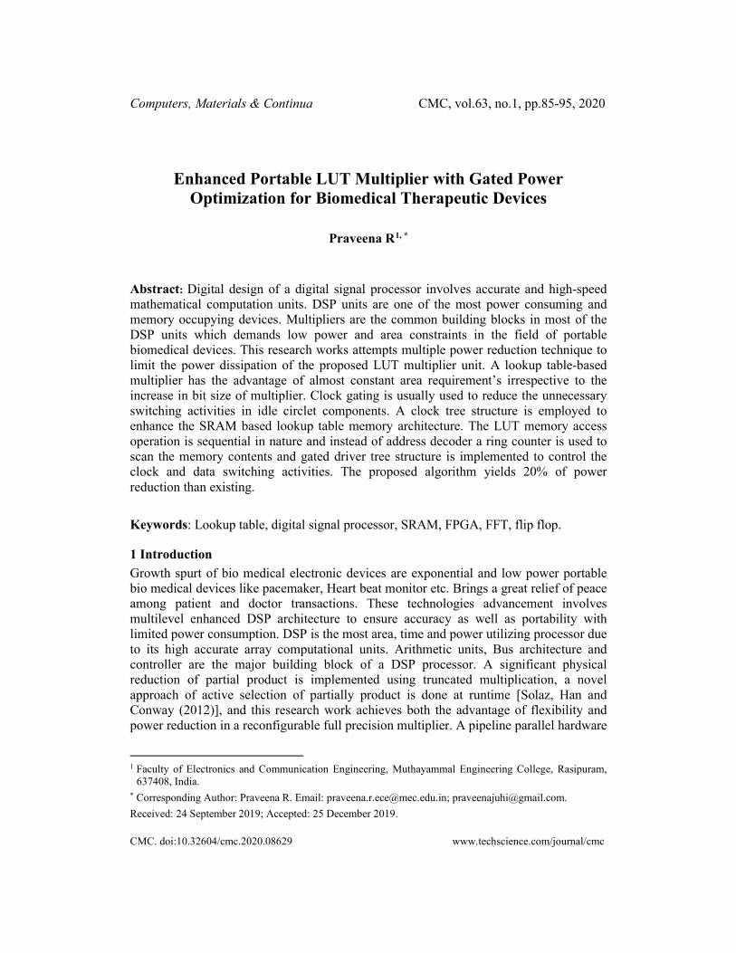
Figure 1: SRAM cell design
A basic SRAM cell structure with read write selection is shown in Fig. 1. whereas for LUT design SRAM cell should be modified as Read only Memory, so r/wbar selection will be always high (read) state.
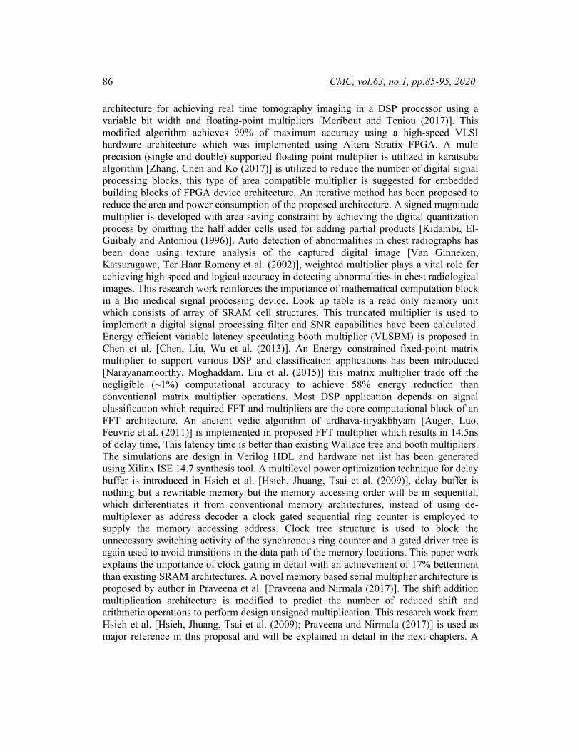
Figure 2: SRAM array for LUT
Fig. 2 represents a 2×2 SRAM array memory block with a conventional address decoder, this address decoder is used to decode the input address lines into SRAM block selection lines, whereas for a LUT design the r/wbar pin will be always High.
Enhanced Portable LUT Multiplier with Gated Power 89
Based on the address decoder input either on the sel0 or sel1 will be activated based on the selection input either the SRAM (00, 01) or SRAM (10, 11) column will be triggered to unload the stored bit in the flip flop. LUT multiplier does not need a write pin so the r/w bar are always activated (read, write) and the data input lines will not be used.
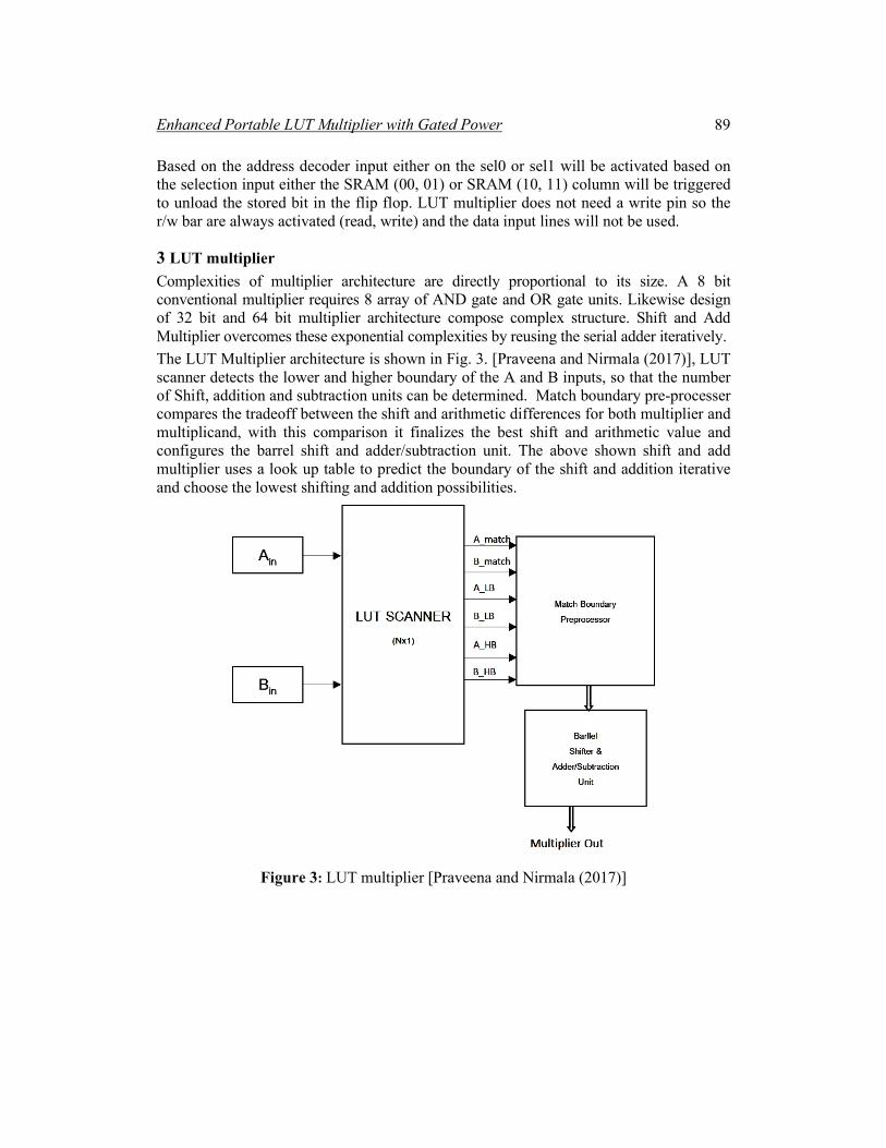
3 LUT multiplier Complexities of multiplier architecture are directly proportional to its size. A 8 bit conventional multiplier requires 8 array of AND gate and OR gate units. Likewise design of 32 bit and 64 bit multiplier architecture compose complex structure. Shift and Add Multiplier overcomes these exponential complexities by reusing the serial adder iteratively. The LUT Multiplier architecture is shown in Fig. 3. [Praveena and Nirmala (2017)], LUT scanner detects the lower and higher boundary of the A and B inputs, so that the number of Shift, addition and subtraction units can be determined. Match boundary pre-processer compares the tradeoff between the shift and arithmetic differences for both multiplier and multiplicand, with this comparison it finalizes the best shift and arithmetic value and configures the barrel shift and adder/subtraction unit. The above shown shift and add multiplier uses a look up table to predict the boundary of the shift and addition iterative and choose the lowest shifting and addition possibilities.
Figure 3: LUT multiplier [Praveena and Nirmala (2017)]
CMC, vol.63, no.1, pp.85-95, 2020 90
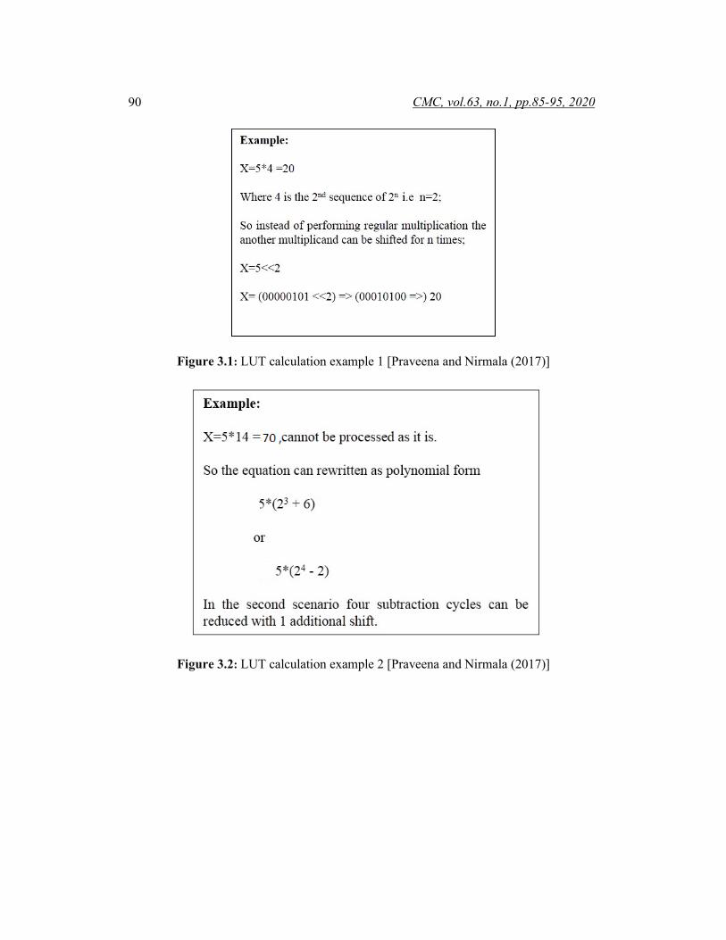
Figure 3.1: LUT calculation example 1 [Praveena and Nirmala (2017)]
Figure 3.2: LUT calculation example 2 [Praveena and Nirmala (2017)]
Enhanced Portable LUT Multiplier with Gated Power 91
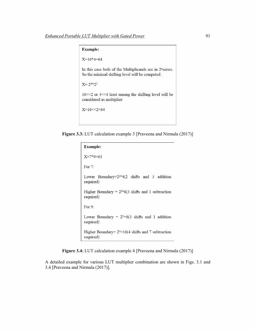
Figure 3.3: LUT calculation example 3 [Praveena and Nirmala (2017)]
Figure 3.4: LUT calculation example 4 [Praveena and Nirmala (2017)]
A detailed example for various LUT multiplier combination are shown in Figs. 3.1 and 3.4 [Praveena and Nirmala (2017)].
CMC, vol.63, no.1, pp.85-95, 2020 92
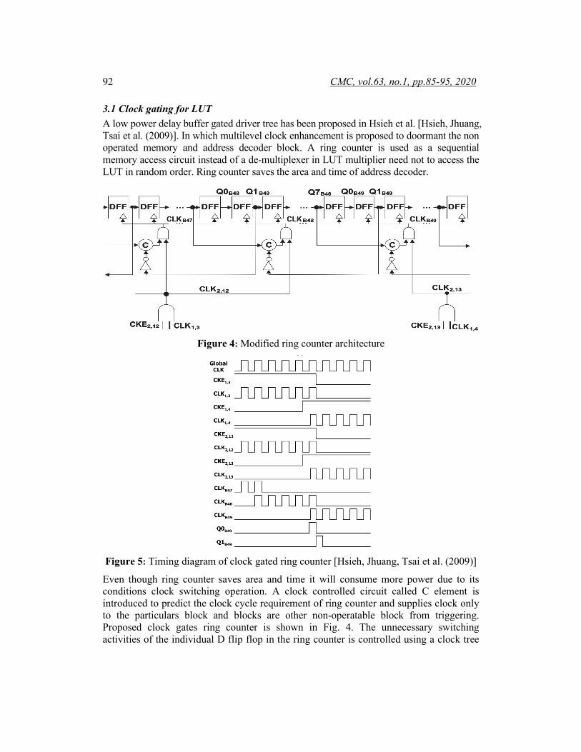
3.1 Clock gating for LUT A low power delay buffer gated driver tree has been proposed in Hsieh et al. [Hsieh, Jhuang, Tsai et al. (2009)]. In which multilevel clock enhancement is proposed to doormant the non operated memory and address decoder block. A ring counter is used as a sequential memory access circuit instead of a de-multiplexer in LUT multiplier need not to access the LUT in random order. Ring counter saves the area and time of address decoder.
Figure 4: Modified ring counter architecture
Figure 5: Timing diagram of clock gated ring counter [Hsieh, Jhuang, Tsai et al. (2009)]
Even though ring counter saves area and time it will consume more power due to its conditions clock switching operation. A clock controlled circuit called C element is introduced to predict the clock cycle requirement of ring counter and supplies clock only to the particulars block and blocks are other non-operatable block from triggering. Proposed clock gates ring counter is shown in Fig. 4. The unnecessary switching activities of the individual D flip flop in the ring counter is controlled using a clock tree
Enhanced Portable LUT Multiplier with Gated Power 93
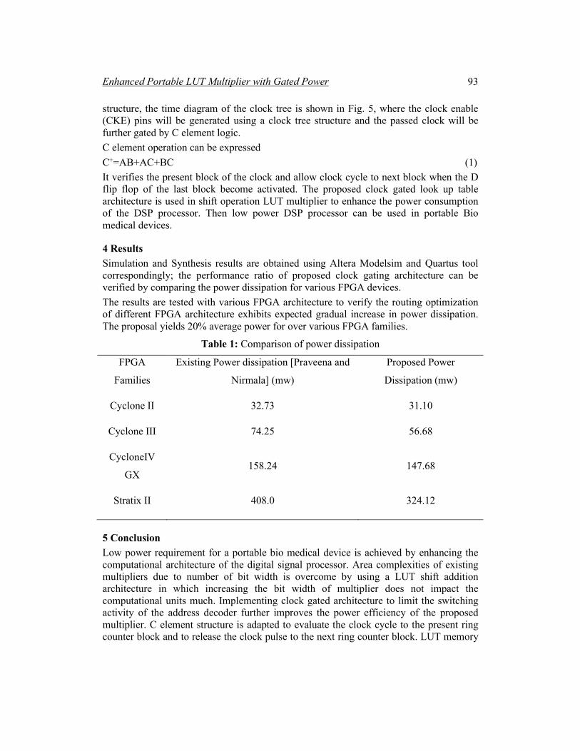
structure, the time diagram of the clock tree is shown in Fig. 5, where the clock enable (CKE) pins will be generated using a clock tree structure and the passed clock will be further gated by C element logic. C element operation can be expressed C+=AB+AC+BC (1) It verifies the present block of the clock and allow clock cycle to next block when the D flip flop of the last block become activated. The proposed clock gated look up table architecture is used in shift operation LUT multiplier to enhance the power consumption of the DSP processor. Then low power DSP processor can be used in portable Bio medical devices.
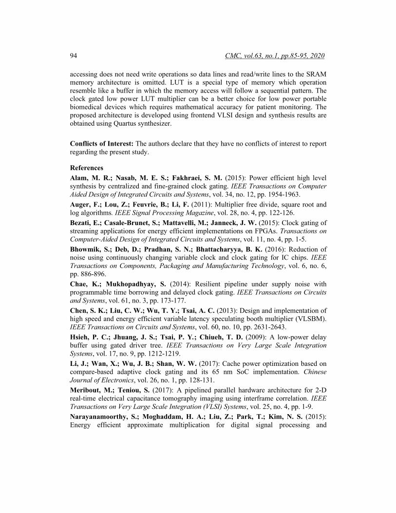
4 Results Simulation and Synthesis results are obtained using Altera Modelsim and Quartus tool correspondingly; the performance ratio of proposed clock gating architecture can be verified by comparing the power dissipation for various FPGA devices. The results are tested with various FPGA architecture to verify the routing optimization of different FPGA architecture exhibits expected gradual increase in power dissipation. The proposal yields 20% average power for over various FPGA families.
Table 1: Comparison of power dissipation
FPGA
Families
Existing Power dissipation [Praveena and
Nirmala] (mw)
Proposed Power
Dissipation (mw)
Cyclone II 32.73 31.10
Cyclone III 74.25 56.68
CycloneIV
GX 158.24 147.68
Stratix II 408.0 324.12
5 Conclusion Low power requirement for a portable bio medical device is achieved by enhancing the computational architecture of the digital signal processor. Area complexities of existing multipliers due to number of bit width is overcome by using a LUT shift addition architecture in which increasing the bit width of multiplier does not impact the computational units much. Implementing clock gated architecture to limit the switching activity of the address decoder further improves the power efficiency of the proposed multiplier. C element structure is adapted to evaluate the clock cycle to the present ring counter block and to release the clock pulse to the next ring counter block. LUT memory
CMC, vol.63, no.1, pp.85-95, 2020 94
accessing does not need write operations so data lines and read/write lines to the SRAM memory architecture is omitted. LUT is a special type of memory which operation resemble like a buffer in which the memory access will follow a sequential pattern. The clock gated low power LUT multiplier can be a better choice for low power portable biomedical devices which requires mathematical accuracy for patient monitoring. The proposed architecture is developed using frontend VLSI design and synthesis results are obtained using Quartus synthesizer. Conflicts of Interest: The authors declare that they have no conflicts of interest to report regarding the present study.
References Alam, M. R.; Nasab, M. E. S.; Fakhraei, S. M. (2015): Power efficient high level synthesis by centralized and fine-grained clock gating. IEEE Transactions on Computer Aided Design of Integrated Circuits and Systems, vol. 34, no. 12, pp. 1954-1963. Auger, F.; Lou, Z.; Feuvrie, B.; Li, F. (2011): Multiplier free divide, square root and log algorithms. IEEE Signal Processing Magazine, vol. 28, no. 4, pp. 122-126. Bezati, E.; Casale-Brunet, S.; Mattavelli, M.; Janneck, J. W. (2015): Clock gating of streaming applications for energy efficient implementations on FPGAs. Transactions on Computer-Aided Design of Integrated Circuits and Systems, vol. 11, no. 4, pp. 1-5. Bhowmik, S.; Deb, D.; Pradhan, S. N.; Bhattacharyya, B. K. (2016): Reduction of noise using continuously changing variable clock and clock gating for IC chips. IEEE Transactions on Components, Packaging and Manufacturing Technology, vol. 6, no. 6, pp. 886-896. Chae, K.; Mukhopadhyay, S. (2014): Resilient pipeline under supply noise with programmable time borrowing and delayed clock gating. IEEE Transactions on Circuits and Systems, vol. 61, no. 3, pp. 173-177. Chen, S. K.; Liu, C. W.; Wu, T. Y.; Tsai, A. C. (2013): Design and implementation of high speed and energy efficient variable latency speculating booth multiplier (VLSBM). IEEE Transactions on Circuits and Systems, vol. 60, no. 10, pp. 2631-2643. Hsieh, P. C.; Jhuang, J. S.; Tsai, P. Y.; Chiueh, T. D. (2009): A low-power delay buffer using gated driver tree. IEEE Transactions on Very Large Scale Integration Systems, vol. 17, no. 9, pp. 1212-1219. Li, J.; Wan, X.; Wu, J. B.; Shan, W. W. (2017): Cache power optimization based on compare-based adaptive clock gating and its 65 nm SoC implementation. Chinese Journal of Electronics, vol. 26, no. 1, pp. 128-131. Meribout, M.; Teniou, S. (2017): A pipelined parallel hardware architecture for 2-D real-time electrical capacitance tomography imaging using interframe correlation. IEEE Transactions on Very Large Scale Integration (VLSI) Systems, vol. 25, no. 4, pp. 1-9. Narayanamoorthy, S.; Moghaddam, H. A.; Liu, Z.; Park, T.; Kim, N. S. (2015): Energy efficient approximate multiplication for digital signal processing and
Enhanced Portable LUT Multiplier with Gated Power 95
classification applications. IEEE Transactions on Very Large Scale Integration Systems, vol. 23, no. 6, pp. 1180-1184. Praveena, R.; Nirmala, S. (2017): Bus encoded LUT multiplier for portable biomedical therapeutic devices. Computers, Materials & Continua, vol. 53, no. 1, pp. 37-47. Solaz, M. G.; Han, W.; Conway, R. (2012): A flexible low power DSP with a programmable truncated multiplier. IEEE Transactions on Circuits and Systems, vol. 59, no. 11, pp. 2555-2568. Kidambi, S. S.; El-Guibaly, F.; Antoniou, A. (1996): Area efficient multipliers for digital signal processing applications. IEEE Transactions on Circuits and Systems Analog and Digital Signal Processing, vol. 43, no. 2, pp. 90-95. Van Ginneken, B.; Katsuragawa, S.; Ter Haar Romeny, B. M.; Doi, K.; Viergever, M. A. (2002): Automatic detection of abnormalities in chest radiographs using local texture analysis. IEEE Transactions on Medical Imaging, vol. 21, no. 2, pp. 139-149. Wimer, S.; Albahari, A. (2014): A look-ahead clock gating based on auto gated flip flops. IEEE Transactions on Circuits and Systems, vol. 61, no. 5, pp. 1465-1472. Zhang, H.; Chen, D.; Ko, S. B. (2017): Area and power efficient iterative single double precision merged floating point multiplier on FPGA. IET Computers and Digital Techniques, vol. 11, no. 4, pp. 149-158.