Embed Size (px)
Citation preview
APL Mater. 7, 071104 (2019); https://doi.org/10.1063/1.5091735 7, 071104
© 2019 Author(s).
Enhanced electro-mechanical coupling ofTiN/Ce0.8Gd0.2O1.9 thin film electrostrictor
Cite as: APL Mater. 7, 071104 (2019); https://doi.org/10.1063/1.5091735Submitted: 05 February 2019 . Accepted: 23 June 2019 . Published Online: 10 July 2019
Simone Santucci , Haiwu Zhang , Simone Sanna , Nini Pryds , and Vincenzo Esposito
APL Materials ARTICLE scitation.org/journal/apm
Enhanced electro-mechanical couplingof TiN/Ce0.8Gd0.2O1.9 thin film electrostrictor
Cite as: APL Mater. 7, 071104 (2019); doi: 10.1063/1.5091735Submitted: 5 February 2019 • Accepted: 23 June 2019 •Published Online: 10 July 2019
Simone Santucci,a) Haiwu Zhang, Simone Sanna, Nini Pryds, and Vincenzo Espositoa)
AFFILIATIONSDepartment of Energy Conversion and Storage, Technical University of Denmark, Frederiksborgvej 399 Roskilde, Denmark
a)Authors to whom correspondence should be addressed: [email protected] and [email protected]
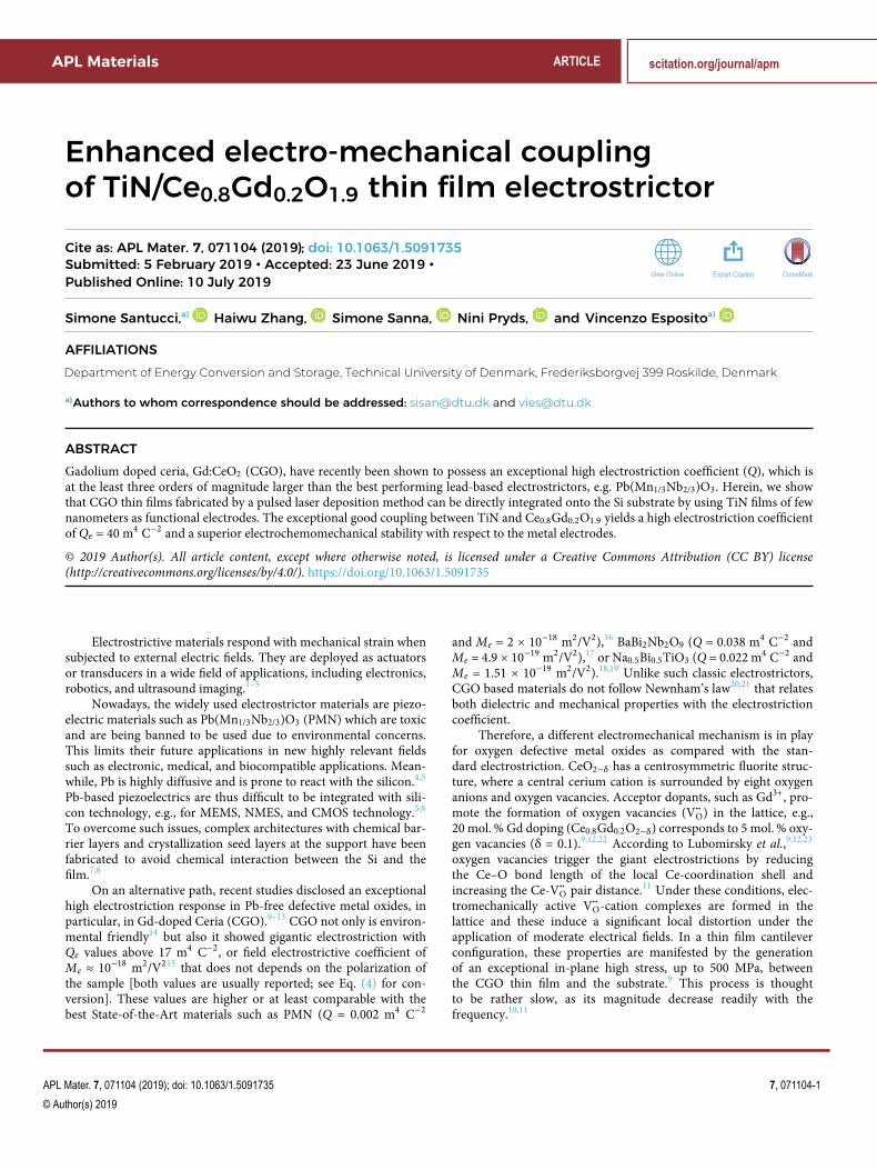
ABSTRACTGadolium doped ceria, Gd:CeO2 (CGO), have recently been shown to possess an exceptional high electrostriction coefficient (Q), which isat the least three orders of magnitude larger than the best performing lead-based electrostrictors, e.g. Pb(Mn1/3Nb2/3)O3. Herein, we showthat CGO thin films fabricated by a pulsed laser deposition method can be directly integrated onto the Si substrate by using TiN films of fewnanometers as functional electrodes. The exceptional good coupling between TiN and Ce0.8Gd0.2O1.9 yields a high electrostriction coefficientof Qe = 40 m4 C−2 and a superior electrochemomechanical stability with respect to the metal electrodes.
© 2019 Author(s). All article content, except where otherwise noted, is licensed under a Creative Commons Attribution (CC BY) license(http://creativecommons.org/licenses/by/4.0/). https://doi.org/10.1063/1.5091735., s
Electrostrictive materials respond with mechanical strain whensubjected to external electric fields. They are deployed as actuatorsor transducers in a wide field of applications, including electronics,robotics, and ultrasound imaging.1–3
Nowadays, the widely used electrostrictor materials are piezo-electric materials such as Pb(Mn1/3Nb2/3)O3 (PMN) which are toxicand are being banned to be used due to environmental concerns.This limits their future applications in new highly relevant fieldssuch as electronic, medical, and biocompatible applications. Mean-while, Pb is highly diffusive and is prone to react with the silicon.4,5
Pb-based piezoelectrics are thus difficult to be integrated with sili-con technology, e.g., for MEMS, NMES, and CMOS technology.5,6
To overcome such issues, complex architectures with chemical bar-rier layers and crystallization seed layers at the support have beenfabricated to avoid chemical interaction between the Si and thefilm.7,8
On an alternative path, recent studies disclosed an exceptionalhigh electrostriction response in Pb-free defective metal oxides, inparticular, in Gd-doped Ceria (CGO).9–13 CGO not only is environ-mental friendly14 but also it showed gigantic electrostriction withQe values above 17 m4 C−2, or field electrostrictive coefficient ofMe ≈ 10−18 m2/V215 that does not depends on the polarization ofthe sample [both values are usually reported; see Eq. (4) for con-version]. These values are higher or at least comparable with thebest State-of-the-Art materials such as PMN (Q = 0.002 m4 C−2
and Me = 2 × 10⁻¹⁸ m2/V2),16 BaBi2Nb2O9 (Q = 0.038 m4 C−2 andMe = 4.9 × 10⁻¹⁹ m2/V2),17 or Na0.5Bi0.5TiO3 (Q = 0.022 m4 C−2 andMe = 1.51 × 10⁻¹⁹ m2/V2).18,19 Unlike such classic electrostrictors,CGO based materials do not follow Newnham’s law20,21 that relatesboth dielectric and mechanical properties with the electrostrictioncoefficient.
Therefore, a different electromechanical mechanism is in playfor oxygen defective metal oxides as compared with the stan-dard electrostriction. CeO2−δ has a centrosymmetric fluorite struc-ture, where a central cerium cation is surrounded by eight oxygenanions and oxygen vacancies. Acceptor dopants, such as Gd3+, pro-mote the formation of oxygen vacancies (V⋅⋅O) in the lattice, e.g.,20 mol. % Gd doping (Ce0.8Gd0.2O2−δ) corresponds to 5 mol. % oxy-gen vacancies (δ = 0.1).9,12,22 According to Lubomirsky et al.,9,12,23
oxygen vacancies trigger the giant electrostrictions by reducingthe Ce–O bond length of the local Ce-coordination shell andincreasing the Ce-V⋅⋅O pair distance.11 Under these conditions, elec-tromechanically active V⋅⋅O-cation complexes are formed in thelattice and these induce a significant local distortion under theapplication of moderate electrical fields. In a thin film cantileverconfiguration, these properties are manifested by the generationof an exceptional in-plane high stress, up to 500 MPa, betweenthe CGO thin film and the substrate.9 This process is thoughtto be rather slow, as its magnitude decrease readily with thefrequency.10,11
APL Mater. 7, 071104 (2019); doi: 10.1063/1.5091735 7, 071104-1
© Author(s) 2019
APL Materials ARTICLE scitation.org/journal/apm
Evidence of such electromechanical performances has beenconfirmed recently by Hadad et al.,24 by depositing CGO thin filmson Si with different metal electrodes (Si/x/CGO/x, x = Al, Pt, Cr).They found that the electromechanical performances and stabil-ity of the CGO thin films depend critically on the electrodes used,making a rigorous characterization of the film itself difficult. CGOelectrostrictive thin films deposited on metal electrodes often showmechanical decoupling during operation due to poor adhesion at theceramic-metallic interface.11,24–26
Furthermore, cerium oxide is a refractory material, and con-versely to Pb-based materials that need chemical barrier layers, itdoes not react with Si/SiO2 substrates and is compatible with manymaterials for both low and high temperature uses.27–29
In this study, in order to overcome these limitations, weincluded Ce0.8Gd0.2O1.9 thin films with titanium nitride (TiN) elec-trodes (TiN/CGO/TiN configuration) by Pulsed Laser Deposition(PLD). TiN has a rock-salt (NaCl) structure and shows excellentmechanical and electrical properties, such as low resistance (σ ≈200 S/cm at room temperature) and high chemical stability.30,31
Therefore, TiN is an ideal candidate for Si integrated technologiesand microelectronics such as electrodes, diffusion barriers, gates,or Schottky barrier contacts.32–35 Coupling CGO with TiN can sig-nificantly simplify the integration procedures of these electrostric-tors with Si-based technologies and microelectronics. Moreover,as a ceramic material, TiN is expected to provide superior crys-tallographic transport matches to CGO and chemical stability. Asfor a comparison, CGO thin films with a Au/CGO/TiN config-uration were also fabricated to analyze stability and degradationbehavior.
The Ce0.8Gd0.2O1.9 target for the deposition was fabricatedby synthetized Ce0.8Gd0.2O1.9 powder following by uniaxial cold-pressing at 140 MPa and then sintered at 1723 K for 10 h. A highpure fluorite phase was observed for the as prepared targets.
CGO films with thicknesses of 800 and 1400 nm were depositedby PLD on a commercial [90 nm TiN/525 µm Si] substrate (PrimeWafers). The wavelength of the excimer laser is 248 nm, with a20 Hz repetition rate, an output energy of 200 mJ, and a fluence of3 J cm−2 (growth rate of 0.05 Å/pulse).28 The deposition temper-ature was set to be 400 C, and the target-substrate distance wasfixed at ∼72 mm. In order to avoid possible oxidation of TiN, the
first 15 min of deposition was carried out with nitrogen flow at 10−3
mbar, after which it was switched to oxygen at 10−3 mbar. Then, forfilms with the TiN/CGO/TiN configuration, TiN was grown by PLDwith a temperature of 600 C and N2 flow at 10−3 mbar. For filmswith the Au/CGO/TiN configuration, the Au top electrode was sput-tered at room temperature with a Bal-Tec SCD 005 Sputter Coater.The samples were cut in beam shape: 7–8 mm wide and 15 mmlong.
XRD analyses were performed with a Bruker D8 on depositedfilms. No secondary phases in the as deposited thin films wereobserved within the resolution limit of the instrument. Microstruc-ture investigation and thickness measurement were carried outwith the Zeiss Gemini-Merlin FE-SEM on the cross section of thesamples.
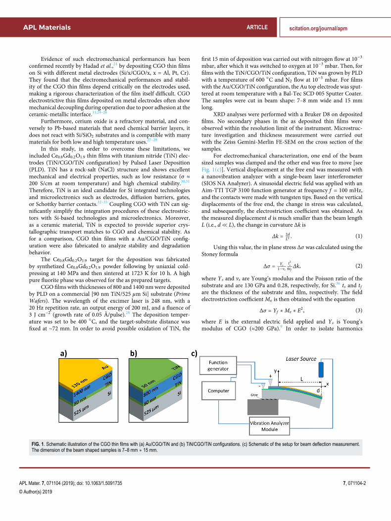
For electromechanical characterization, one end of the beamsized samples was clamped and the other end was free to move [seeFig. 1(c)]. Vertical displacement at the free end was measured witha nanovibration analyzer with a single-beam laser interferometer(SIOS NA Analyzer). A sinusoidal electric field was applied with anAim-TTI TGP 3100 function generator at frequency f = 100 mHz,and the contacts were made with tungsten tips. Based on the verticaldisplacements of the free end, the change in stress was calculated,and subsequently, the electrostriction coefficient was obtained. Asthe measured displacement d is much smaller than the beam lengthL (i.e., d≪ L), the change in curvature ∆k is
∆k = 2dL2 . (1)
Using this value, the in plane stress ∆σ was calculated using theStoney formula
∆σ = Ys1−vs
t2s
6tf∆k, (2)
where Y s and vs are Young’s modulus and the Poisson ratio of thesubstrate and are 130 GPa and 0.28, respectively, for Si.36 ts and tfare the thickness of the substrate and film, respectively. The fieldelectrostriction coefficient Me is then obtained with the equation
∆σ = Yf ∗Me ∗ E2, (3)
where E is the external electric field applied and Y s is Young’smodulus of CGO (≈200 GPa).9 In order to isolate harmonics
FIG. 1. Schematic illustration of the CGO thin films with (a) Au/CGO/TiN and (b) TiN/CGO/TiN configurations. (c) Schematic of the setup for beam deflection measurement.The dimension of the beam shaped samples is 7–8 mm ∗ 15 mm.
APL Mater. 7, 071104 (2019); doi: 10.1063/1.5091735 7, 071104-2
© Author(s) 2019
APL Materials ARTICLE scitation.org/journal/apm
oscillation, the signal was smoothed and the mechanical drift of theinterferometer removed with a linear fit of the background.
Although the polarization electrostriction coefficient (Qe) isgenerally used to describe the classic electrostrictors, the field elec-trostriction coefficient (Me) is preferably used in the experimentalprocedure, as it is related to the electric field instead of polarization.Me and Qe coefficients are related by the equation
Me = Qeε0(εr − 1)2, (4)
where ε0 is the vacuum permittivity and εr is the relative dielectricconstant of CGO (≈28).9,12,37,38 During the experiment, we trackedpotential temperature variation with a FLIR SC5000 thermal camerawith a waveband of 2.5–5.1 µm and 20 mK sensitivity.
The film quality is generally improved by increasing the tem-perature at the substrate (Ts) above 400 C and by reducing theoxygen partial pressure (pO2) within the PLD deposition cham-ber.28,39,40 The substrate temperature (Ts) during PLD is a particu-larly important parameter to achieve high density of the CGO thinfilms, ensuring mechanical continuity of the electrostrictive film.41
High crystallographic order is achieved, as CGO is deposited onstructurally similar substrates with similar lattice parameters.41,42 Onthe other hand, Infortuna et al.39 found that pO2 < 5 × 10⁻² mbarpromotes a dense columnar structure in CGO, above which dis-ordered and porous microstructures were observed. The top TiNelectrode was deposited at 600 C to increase conductivity,43 avoid-ing residual strain.44 During the deposition, N2 flow was used toavoid oxygen inclusion43 and the variation of the stoichiometry ofTiN. The correct stoichiometry was confirmed by XRD (Fig. S1 ofthe supplementary material).
Figures 1(a) and 1(b) schematically illustrate the configura-tions of Au/CGO/TiN and TiN/CGO/TiN, respectively. Structuraland microstructural analyses reveal that the thickness of the bottomTiN electrode is 80 nm and the thickness of Ce0.8Gd0.2O1.9 withinAu/CGO/TiN and TiN/CGO/TiN thin films are 800 and 1400 nm,respectively (Fig. S2 of the supplementary material). The top elec-trode in the former (Au) and the latter (TiN) is 120 and 50 nm,respectively. The CGO layers exhibit a preferred (111) orientation(Fig. S1 of the supplementary material), as consistent with that pre-pared by RF sputtering,10,24 and show a columnar structure with nodetectable porosity. The electromechanical characterization with acantilever vibration setup is shown in Fig. 1(c).
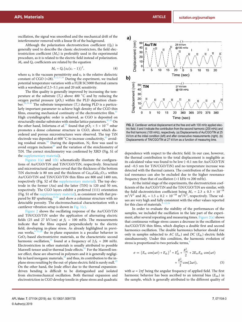
Figure 2 shows the oscillating response of the Au/CGO/TiNand TiN/CGO/TiN under the application of alternating electricfields (25 and 27 kV/cm) at fE = 100 mHz. The measurementsindicate that the films expand perpendicularly to the electricfield, developing in-plane stress. As already highlighted in previ-ous works,9–11,24 the in-plane expansion is a peculiar behavior inCeO2-based electrostrictive materials, as the characteristic secondharmonic oscillation,21 found at a frequency of 2⋅fE = 200 mHz.Electrostriction in other materials is usually attributed to possibleMaxwell-tensor and/or thermal Joule effects.45 For the Maxwell ten-sor effect, these are observed in polymers and it is generally negligi-ble in hard inorganic materials,46 and thus, its contribution to the in-plane stress resulting by the out-of-plane electric field is surely null.45
On the other hand, the Joule effect due to the thermal expansion-driven bending is difficult to be distinguished and isolatedfrom electromechanical oscillation. Both thermal expansion andelectrostriction in CGO develop tensile in-plane stress and quadratic
FIG. 2. Cantilever vertical displacement at the free end with 100 mHz applied elec-tric field. II and I indicate the contribution from the second harmonic (200 mHz) andthe first harmonic (100 mHz), respectively. (a) Displacements of Au/CGO/TiN at 25kV/cm at the initial condition (left) and after consecutive measurements (right). (b)Displacements of TiN/CGO/TiN at 27 kV/cm as a function of measuring time.
dependence with respect to the electric field. In our case, however,the thermal contribution to the total displacement is negligible asits calculated value was found to be low (∼0.1 nm for Au/CGO/TiNand ∼0.5 nm for TiN/CGO/TiN) and no temperature increase wasdetected with the thermal camera. The contribution of the mechan-ical resonance can also be excluded due to the higher resonancefrequency than that of oscillation (>1 kHz vs 200 mHz).
At the initial stage of the experiments, the electrostriction coef-ficients of the Au/CGO/TiN and the TiN/CGO/TiN are similar, withthe field electrostriction coefficient being Me = 2.3 ± 0.3 × 10⁻¹⁸
m2/V2 and Me = 1.5 ± 0.2 × 10⁻¹⁸ m2/V2, respectively. These val-ues are very high and fully consistent with the other values reportedfor this class of materials.9–12,24
In order to evaluate the stability of the performances of thesamples, we included the oscillation in the late part of the experi-ment, after several repeating and measuring times. Figure 2(a) showsthat continuous voltage stress causes a decrease in the oscillation ofAu/CGO/TiN thin films, which displays a double first and secondharmonics oscillation. The double harmonics behavior should riseonly in samples subjected to AC (Eac) and DC (Edc) electric fieldssimultaneously. Under this condition, the harmonic evolution ofstress is proportional to two periodic terms,9
σ∝ Eac cos(ωt) + Edc2 = E2dc +
E2ac
2+ 2EacEdc cos(ωt)
+E2ac
2cos(2ωt), (5)
with ω = 2πf being the angular frequency of applied field. The firstharmonic behavior has been ascribed to an internal bias (Eint) inthe sample, which is generally attributed to the different quality of
APL Mater. 7, 071104 (2019); doi: 10.1063/1.5091735 7, 071104-3
© Author(s) 2019
APL Materials ARTICLE scitation.org/journal/apm
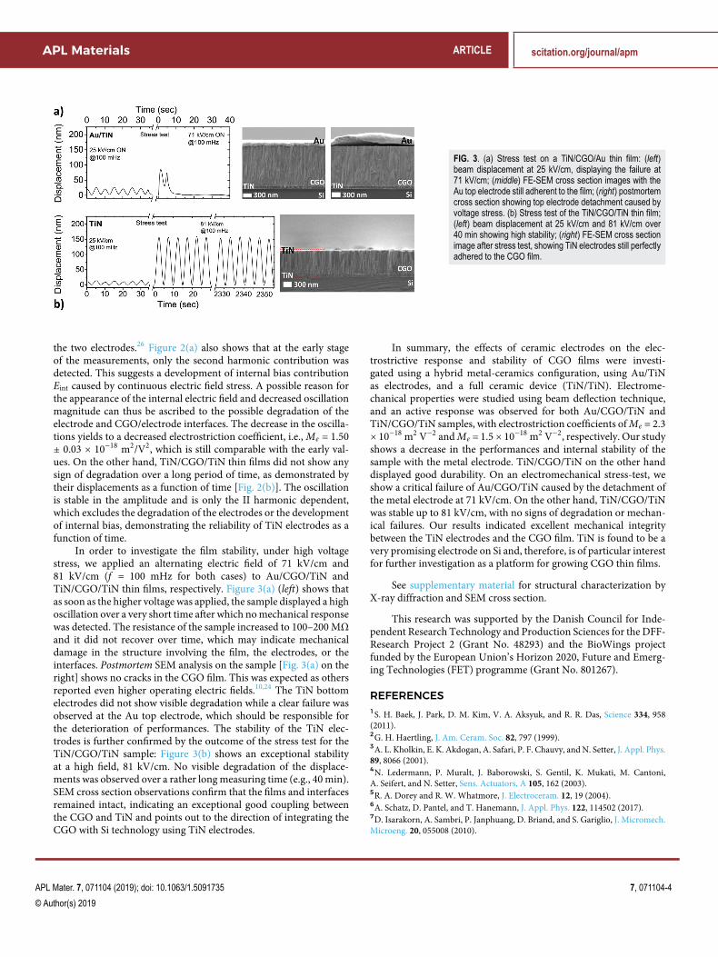
FIG. 3. (a) Stress test on a TiN/CGO/Au thin film: (left)beam displacement at 25 kV/cm, displaying the failure at71 kV/cm; (middle) FE-SEM cross section images with theAu top electrode still adherent to the film; (right) postmortemcross section showing top electrode detachment caused byvoltage stress. (b) Stress test of the TiN/CGO/TiN thin film;(left) beam displacement at 25 kV/cm and 81 kV/cm over40 min showing high stability; (right) FE-SEM cross sectionimage after stress test, showing TiN electrodes still perfectlyadhered to the CGO film.
the two electrodes.26 Figure 2(a) also shows that at the early stageof the measurements, only the second harmonic contribution wasdetected. This suggests a development of internal bias contributionEint caused by continuous electric field stress. A possible reason forthe appearance of the internal electric field and decreased oscillationmagnitude can thus be ascribed to the possible degradation of theelectrode and CGO/electrode interfaces. The decrease in the oscilla-tions yields to a decreased electrostriction coefficient, i.e., Me = 1.50± 0.03 × 10⁻¹⁸ m2/V2, which is still comparable with the early val-ues. On the other hand, TiN/CGO/TiN thin films did not show anysign of degradation over a long period of time, as demonstrated bytheir displacements as a function of time [Fig. 2(b)]. The oscillationis stable in the amplitude and is only the II harmonic dependent,which excludes the degradation of the electrodes or the developmentof internal bias, demonstrating the reliability of TiN electrodes as afunction of time.
In order to investigate the film stability, under high voltagestress, we applied an alternating electric field of 71 kV/cm and81 kV/cm (f = 100 mHz for both cases) to Au/CGO/TiN andTiN/CGO/TiN thin films, respectively. Figure 3(a) (left) shows thatas soon as the higher voltage was applied, the sample displayed a highoscillation over a very short time after which no mechanical responsewas detected. The resistance of the sample increased to 100–200 MΩand it did not recover over time, which may indicate mechanicaldamage in the structure involving the film, the electrodes, or theinterfaces. Postmortem SEM analysis on the sample [Fig. 3(a) on theright] shows no cracks in the CGO film. This was expected as othersreported even higher operating electric fields.10,24 The TiN bottomelectrodes did not show visible degradation while a clear failure wasobserved at the Au top electrode, which should be responsible forthe deterioration of performances. The stability of the TiN elec-trodes is further confirmed by the outcome of the stress test for theTiN/CGO/TiN sample: Figure 3(b) shows an exceptional stabilityat a high field, 81 kV/cm. No visible degradation of the displace-ments was observed over a rather long measuring time (e.g., 40 min).SEM cross section observations confirm that the films and interfacesremained intact, indicating an exceptional good coupling betweenthe CGO and TiN and points out to the direction of integrating theCGO with Si technology using TiN electrodes.
In summary, the effects of ceramic electrodes on the elec-trostrictive response and stability of CGO films were investi-gated using a hybrid metal-ceramics configuration, using Au/TiNas electrodes, and a full ceramic device (TiN/TiN). Electrome-chanical properties were studied using beam deflection technique,and an active response was observed for both Au/CGO/TiN andTiN/CGO/TiN samples, with electrostriction coefficients of Me = 2.3× 10⁻¹⁸ m2 V−2 andMe = 1.5× 10⁻¹⁸ m2 V−2, respectively. Our studyshows a decrease in the performances and internal stability of thesample with the metal electrode. TiN/CGO/TiN on the other handdisplayed good durability. On an electromechanical stress-test, weshow a critical failure of Au/CGO/TiN caused by the detachment ofthe metal electrode at 71 kV/cm. On the other hand, TiN/CGO/TiNwas stable up to 81 kV/cm, with no signs of degradation or mechan-ical failures. Our results indicated excellent mechanical integritybetween the TiN electrodes and the CGO film. TiN is found to be avery promising electrode on Si and, therefore, is of particular interestfor further investigation as a platform for growing CGO thin films.
See supplementary material for structural characterization byX-ray diffraction and SEM cross section.
This research was supported by the Danish Council for Inde-pendent Research Technology and Production Sciences for the DFF-Research Project 2 (Grant No. 48293) and the BioWings projectfunded by the European Union’s Horizon 2020, Future and Emerg-ing Technologies (FET) programme (Grant No. 801267).
REFERENCES1S. H. Baek, J. Park, D. M. Kim, V. A. Aksyuk, and R. R. Das, Science 334, 958(2011).2G. H. Haertling, J. Am. Ceram. Soc. 82, 797 (1999).3A. L. Kholkin, E. K. Akdogan, A. Safari, P. F. Chauvy, and N. Setter, J. Appl. Phys.89, 8066 (2001).4N. Ledermann, P. Muralt, J. Baborowski, S. Gentil, K. Mukati, M. Cantoni,A. Seifert, and N. Setter, Sens. Actuators, A 105, 162 (2003).5R. A. Dorey and R. W. Whatmore, J. Electroceram. 12, 19 (2004).6A. Schatz, D. Pantel, and T. Hanemann, J. Appl. Phys. 122, 114502 (2017).7D. Isarakorn, A. Sambri, P. Janphuang, D. Briand, and S. Gariglio, J. Micromech.Microeng. 20, 055008 (2010).
APL Mater. 7, 071104 (2019); doi: 10.1063/1.5091735 7, 071104-4
© Author(s) 2019
APL Materials ARTICLE scitation.org/journal/apm
8M. D. Nguyen, H. Yuan, E. P. Houwman, M. Dekkers, G. Koster, J. E. ten Elshof,and G. Rijnders, ACS Appl. Mater. Interfaces 8, 31120 (2016).9R. Korobko, A. Patlolla, A. Kossoy, E. Wachtel, H. L. Tuller, A. I. Frenkel, andI. Lubomirsky, Adv. Mater. 24, 5857 (2012).10R. Korobko, E. Wachtel, and I. Lubomirsky, Sens. Actuators, A 201, 73 (2013).11A. D. Ushakov, N. Yavo, E. Mishuk, I. Lubomirsky, V. Y. Shur, and A. L.Kholkin, KnE Mater. Sci. 1, 177 (2016).12R. Korobko, A. Lerner, Y. Li, E. Wachtel, A. I. Frenkel, and I. Lubomirsky, Appl.Phys. Lett. 106, 042904 (2015).13A. Kabir, S. Santucci, N. Van Nong, M. Varenik, I. Lubomirsky, R. Nigon,P. Muralt, and V. Esposito, Acta Mater. 174, 53 (2019).14C. Sun, H. Li, and L. Chen, Energy Environ. Sci. 5, 8475 (2012).15A. Kossoy, Q. Wang, R. Korobko, V. Grover, Y. Feldman, E. Wachtel, A. K.Tyagi, A. I. Frenkel, and I. Lubomirsky, Phys. Rev. B 87, 054101 (2013).16R. E. N. V. Sundar, J.-F. Li, and D. Viehland, Mater. Res. Bull. 31, 555 (1996).17F. Li, L. Jin, Z. Xu, and S. Zhang, Appl. Phys. Rev. 1, 011103 (2014).18A. You, M. A. Y. Be, and I. In, 202902, 0 (2017).19A. Hussain, A. Maqbool, R. A. Malik, M. H. Kim, T. K. Song, and W. J. Kim,IOP Conf. Ser.: Mater. Sci. Eng. 146, 012006 (2016).20N. Yavo, A. D. Smith, O. Yeheskel, S. Cohen, R. Korobko, E. Wachtel, P. R.Slater, and I. Lubomirsky, Adv. Funct. Mater. 26, 1138 (2016).21R. E. Newnham, V. Sundar, R. Yimnirun, J. Su, and Q. M. Zhang, J. Phys. Chem.B 101, 10141 (1997).22E. Wachtel and I. Lubomirsky, Scr. Mater. 65, 112 (2011).23Y. Li, O. Kraynis, J. Kas, T. C. Weng, D. Sokaras, R. Zacharowicz, I. Lubomirsky,and A. I. Frenkel, AIP Adv. 6, 055320 (2016).24M. Hadad, H. Ashraf, G. Mohanty, C. Sandu, and P. Muralt, Acta Mater. 118, 1(2016).25E. Mishuk, E. Makagon, E. Wachtel, S. R. Cohen, R. Popovitz-Biro, andI. Lubomirsky, Sens. Actuators, A 264, 333 (2017).26A. D. Ushakov, E. Mishuk, E. Makagon, D. O. Alikin, A. A. Esin, I. S. Baturin,A. Tselev, V. Y. Shur, I. Lubomirsky, and A. L. Kholkin, Appl. Phys. Lett. 110,142902 (2017).27A. Bieberle-Hütter, J. L. Hertz, and H. L. Tuller, Acta Mater. 56, 177 (2008).
28N. Pryds, K. Rodrigo, S. Linderoth, and J. Schou, Appl. Surf. Sci. 255, 5232(2009).29V. Esposito, D. W. Ni, S. Sanna, F. Gualandris, and N. Pryds, RSC Adv. 7, 13784(2017).30J. E. Sundgren, Thin Solid Films 128, 21 (1985).31N. K. Ponon, D. J. R. Appleby, E. Arac, P. J. King, S. Ganti, K. S. K. Kwa, andA. O. Neill, Thin Solid Films 578, 31 (2015).32R. H. Dauskardt, M. Lane, Q. Ma, and N. Krishna, Eng. Fract. Mech. 61, 141(1998).33M. C. Lemme, J. K. Efavi, T. Mollenhauer, M. Schmidt, H. D. B. Gottlob,T. Wahlbrink, and H. Kurz, Microelectron. Eng. 83, 1551 (2006).34M. Lukosius, C. Walczyk, M. Fraschke, D. Wolansky, H. Richter, andC. Wenger, Thin Solid Films 518, 4380 (2010).35C. N. Kirchner, H. Hallmeier, R. Szargan, T. Raschke, and C. Radehaus,Electroanalysis 19, 1023 (2007).36M. A. Hopcroft, W. D. Nix, and T. W. Kenny, J. Microelectromech. Syst. 19, 229(2010).37V. Shelukhin, I. Zon, E. Wachtel, Y. Feldman, and I. Lubomirsky, Solid StateIonics 211, 12 (2012).38S. Kim and J. Maier, J. Electrochem. Soc. 149, J73 (2002).39A. Infortuna, A. S. Harvey, and L. J. Gauckler, Adv. Funct. Mater. 18, 127(2008).40J. Schou, Appl. Surf. Sci. 255, 5191 (2009).41S. Sanna, V. Esposito, D. Pergolesi, A. Orsini, A. Tebano, S. Licoccia,G. Balestrino, and E. Traversa, Adv. Funct. Mater. 19, 1713 (2009).42K. Rodrigo, S. Heiroth, M. Lundberg, N. Bonanos, K. Mohan Kant, N. Pryds,L. Theil Kuhn, V. Esposito, S. Linderoth, J. Schou, and T. Lippert, Appl. Phys. A101, 601 (2010).43R. Chowdhury, R. D. Vispute, K. Jagannadham, and J. Narayan, J. Mater. Res.11, 1458 (1996).44D. Rasic, R. Sachan, M. F. Chisholm, J. Prater, and J. Narayan, Cryst. GrowthDes. 17, 6634 (2017).45Y. M. Shkel and D. J. Klingenberg, J. Appl. Phys. 80, 4566 (1996).46L. Liu and P. Sharma, J. Mech. Phys. Solids 112, 1 (2018).
APL Mater. 7, 071104 (2019); doi: 10.1063/1.5091735 7, 071104-5
© Author(s) 2019