Embed Size (px)
Citation preview
ENG/PHYS3320: R.I. Hornsey Fab: 1
ENG/PHYS3320Microsystems Technology
Chapter 2Fabrication of Microsystems
ENG/PHYS3320: R.I. Hornsey Fab: 2
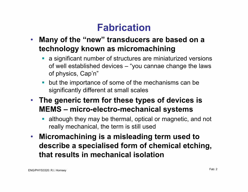
Fabrication• Many of the “new” transducers are based on a
technology known as micromachiningß a significant number of structures are miniaturized versions
of well established devices – “you cannae change the lawsof physics, Cap’n”
ß but the importance of some of the mechanisms can besignificantly different at small scales
• The generic term for these types of devices isMEMS – micro-electro-mechanical systemsß although they may be thermal, optical or magnetic, and not
really mechanical, the term is still used
• Micromachining is a misleading term used todescribe a specialised form of chemical etching,that results in mechanical isolation
ENG/PHYS3320: R.I. Hornsey Fab: 3
• As we discussed in the introduction, the optionsfor our design are limited by compatibility withthe CMOS fabrication processß what we get as part of the CMOS
ß and what we can do afterwards without damaging the CMOS
• A review of the basic CMOS process can befound in books such as Microelectronic Circuits,by Sedra and Smithß we will do a really quick overview here
ENG/PHYS3320: R.I. Hornsey Fab: 4
CMOS technology• Complementary Metal-Oxide-Semiconductorß complementary = two ‘opposite’ types; one conducts with
electrons and one with holes
ß one controlled by making gate = logical 1, other by makinggate = logical 0
ß major advantages is that when both devices are used,current does not flow continuously, so they are low power
• By far the majority of chips are made in CMOStechnologyß process characterised my minimum gate length, e.g. 0.18µm
ENG/PHYS3320: R.I. Hornsey Fab: 5
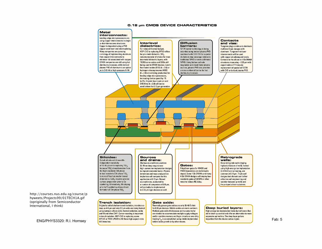
http://courses.nus.edu.sg/course/phyweets/Projects99/01TECH1A.gif(opriginally from SemiconductorInternational, I think)
ENG/PHYS3320: R.I. Hornsey Fab: 6
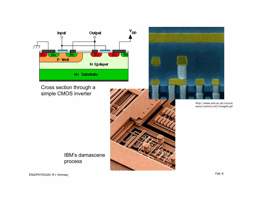
Cross section through asimple CMOS inverter
IBM’s damasceneprocess
http://www.ami.ac.uk/courseware/comms/ch2/image6.gif
ENG/PHYS3320: R.I. Hornsey Fab: 7
• In a standard CMOS process, we get severalmaterials that can be used for micromachiningß silicon substrate (with a variety of doping levels)
ß silicon dioxide – either thin (~5nm) or thick (~1µm) layers
ß polycrystalline silicon (~1µm)
ß aluminum – several layers of various thicknesses
ß possibly other materials, such as silicon nitride and, morerecently, copper
ENG/PHYS3320: R.I. Hornsey Fab: 8
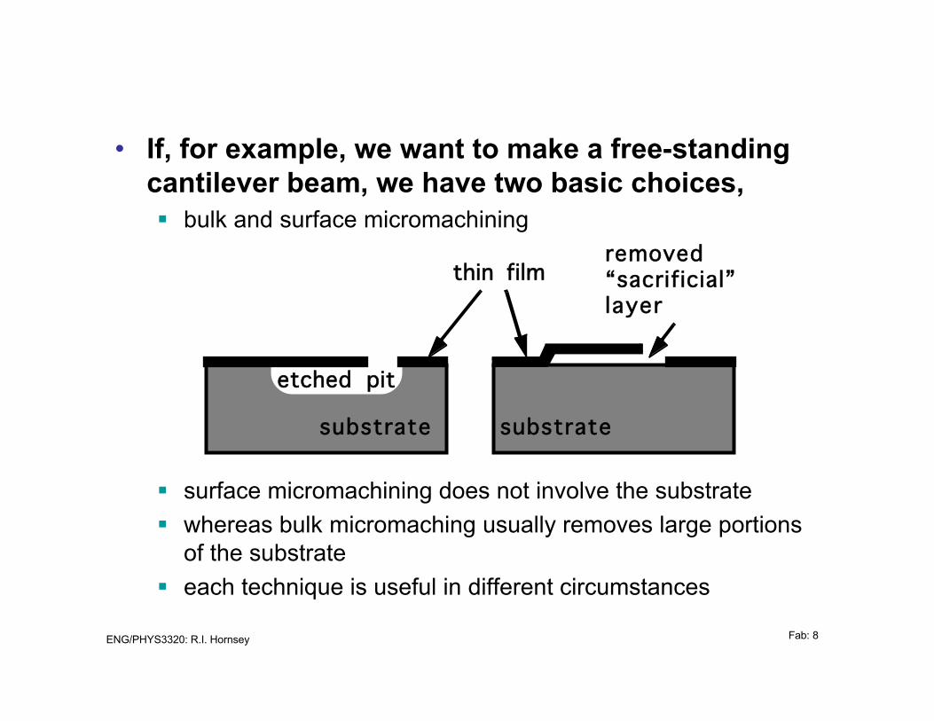
• If, for example, we want to make a free-standingcantilever beam, we have two basic choices,ß bulk and surface micromachining
ß surface micromachining does not involve the substrate
ß whereas bulk micromaching usually removes large portionsof the substrate
ß each technique is useful in different circumstances
thin film
etched pit
removed“sacrificial”layer
substrate substrate
ENG/PHYS3320: R.I. Hornsey Fab: 9
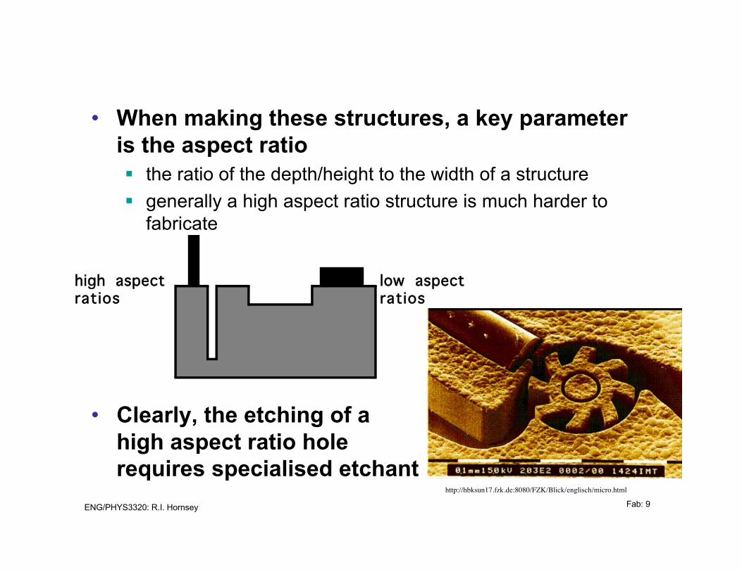
• When making these structures, a key parameteris the aspect ratioß the ratio of the depth/height to the width of a structure
ß generally a high aspect ratio structure is much harder tofabricate
• Clearly, the etching of ahigh aspect ratio holerequires specialised etchant
low aspectratios
high aspectratios
http://hbksun17.fzk.de:8080/FZK/Blick/englisch/micro.html
ENG/PHYS3320: R.I. Hornsey Fab: 10
• Etchants can be categorized as,ß isotropic etchants progress with almost equal rates in all
directions and tend to give rounded corners
ß anisotropic etchants favour a particular direction and hencegive well-defined structures
• They can also be divided in to wet and dryetchantsß wet etching is performed using liquid chemicals
ß dry etching uses physical processes, sometimes with theassistance of gaseous chemical processes
• There are a myriad of individual techniques, thechoice of which depends on numerous factorsß and we will look at just the most common ones
ENG/PHYS3320: R.I. Hornsey Fab: 11
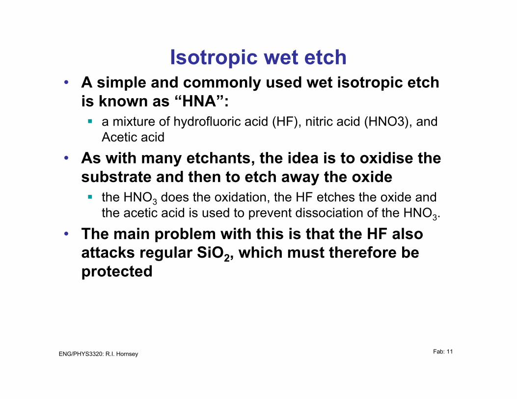
Isotropic wet etch• A simple and commonly used wet isotropic etch
is known as “HNA”:ß a mixture of hydrofluoric acid (HF), nitric acid (HNO3), and
Acetic acid
• As with many etchants, the idea is to oxidise thesubstrate and then to etch away the oxideß the HNO3 does the oxidation, the HF etches the oxide and
the acetic acid is used to prevent dissociation of the HNO3.
• The main problem with this is that the HF alsoattacks regular SiO2, which must therefore beprotected
ENG/PHYS3320: R.I. Hornsey Fab: 12
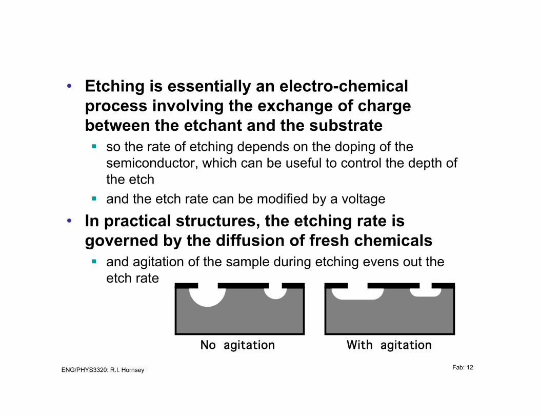
• Etching is essentially an electro-chemicalprocess involving the exchange of chargebetween the etchant and the substrateß so the rate of etching depends on the doping of the
semiconductor, which can be useful to control the depth ofthe etch
ß and the etch rate can be modified by a voltage
• In practical structures, the etching rate isgoverned by the diffusion of fresh chemicalsß and agitation of the sample during etching evens out the
etch rate
No agitation With agitation
ENG/PHYS3320: R.I. Hornsey Fab: 13
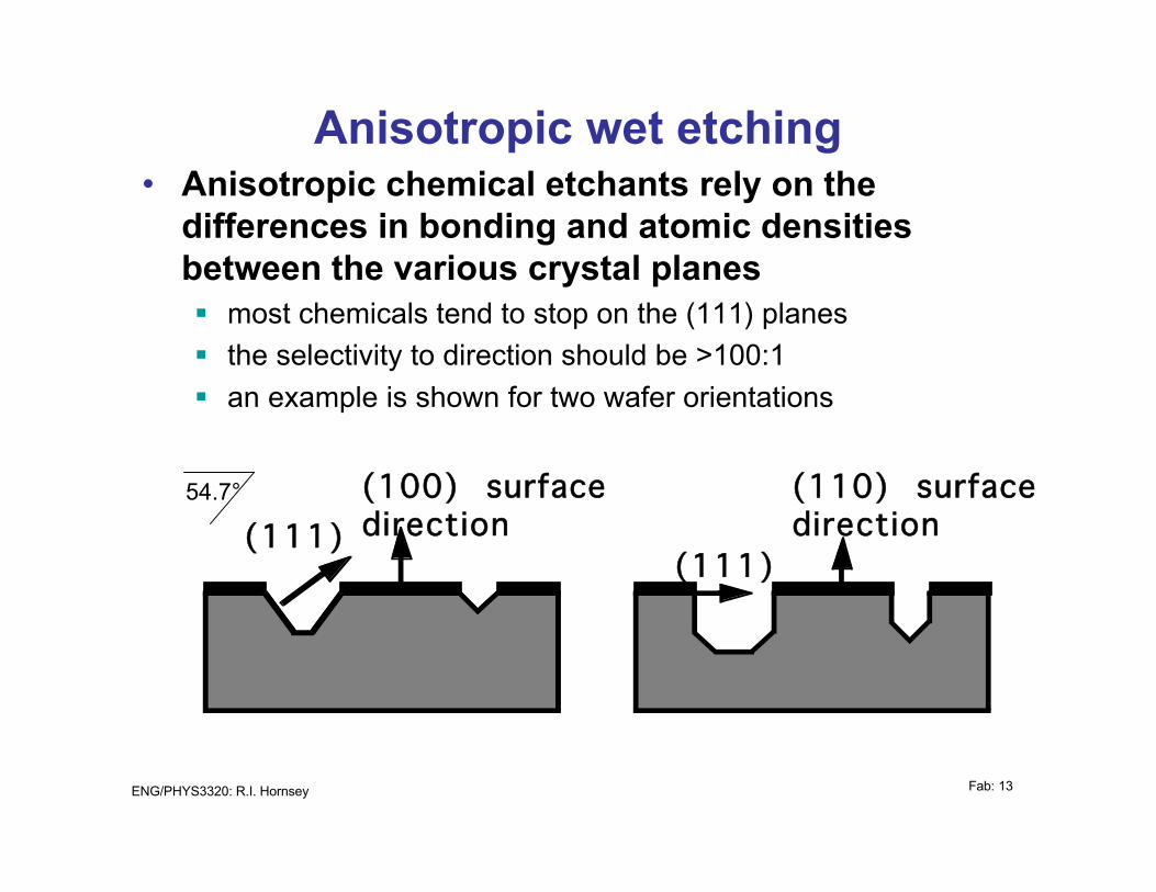
Anisotropic wet etching• Anisotropic chemical etchants rely on the
differences in bonding and atomic densitiesbetween the various crystal planesß most chemicals tend to stop on the (111) planes
ß the selectivity to direction should be >100:1
ß an example is shown for two wafer orientations
(100) surfacedirection(111)
(110) surfacedirection
(111)
54.7°
ENG/PHYS3320: R.I. Hornsey Fab: 14
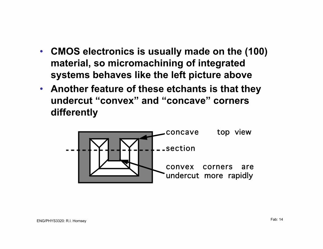
• CMOS electronics is usually made on the (100)material, so micromachining of integratedsystems behaves like the left picture above
• Another feature of these etchants is that theyundercut “convex” and “concave” cornersdifferently
concave
convex corners areundercut more rapidly
section
top view
ENG/PHYS3320: R.I. Hornsey Fab: 15
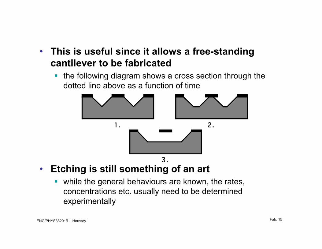
• This is useful since it allows a free-standingcantilever to be fabricatedß the following diagram shows a cross section through the
dotted line above as a function of time
• Etching is still something of an artß while the general behaviours are known, the rates,
concentrations etc. usually need to be determinedexperimentally
1. 2.
3.
ENG/PHYS3320: R.I. Hornsey Fab: 16
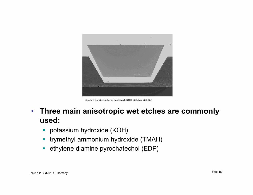
• Three main anisotropic wet etches are commonlyused:ß potassium hydroxide (KOH)
ß trymethyl ammonium hydroxide (TMAH)
ß ethylene diamine pyrochatechol (EDP)
http://www-mat.ee.tu-berlin.de/research/KOH_etch/koh_etch.htm
ENG/PHYS3320: R.I. Hornsey Fab: 17
KOH• (100) plane etched at typically 1µm per minute
• (100) plane is etched 400 times faster than the(111) planeß this allows very long etches, enough to do “back thinning” of
silicon wafers
• Etching slows down in boron (p-) doped regionsß ~1019 cm-3 level
• Etching of SiO2 is typically 1nm/min.
• A potential disadvantage to KOH is the K, whichcan contaminate the CMOS processß so sometimes ammonium hydroxide is used instead
ß but the etch rate is lower and ammonia is given off
ENG/PHYS3320: R.I. Hornsey Fab: 18
TMAH• TMAH is currently the most popular etchant for
use on CMOS substratesß it is cheap, controllable, does not etch aluminum or SiO2,
and is less toxic than the alternatives
• A disadvantage is that the directional selectivityis only about 20ß hence, TMAH is only suitable for relatively shallow structures
• Again, the etch slows for p+ regionsß with a doping of ~1020 cm-3
ENG/PHYS3320: R.I. Hornsey Fab: 19
EDP• Formerly popular anisotropic etch with a
selectivity to direction of about 40:1
• It is less used for integrated systems becauseß it is very carcinogenic
ß it can attack aluminum conductors
ß is corrosive to equipment
ENG/PHYS3320: R.I. Hornsey Fab: 20
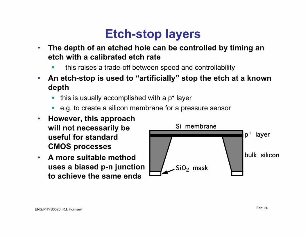
Etch-stop layers• The depth of an etched hole can be controlled by timing an
etch with a calibrated etch rateß this raises a trade-off between speed and controllability
• An etch-stop is used to “artificially” stop the etch at a knowndepthß this is usually accomplished with a p+ layer
ß e.g. to create a silicon membrane for a pressure sensor
• However, this approachwill not necessarily beuseful for standardCMOS processes
• A more suitable methoduses a biased p-n junctionto achieve the same ends
SiO2 mask
bulk silicon
p+ layerSi membrane
ENG/PHYS3320: R.I. Hornsey Fab: 21
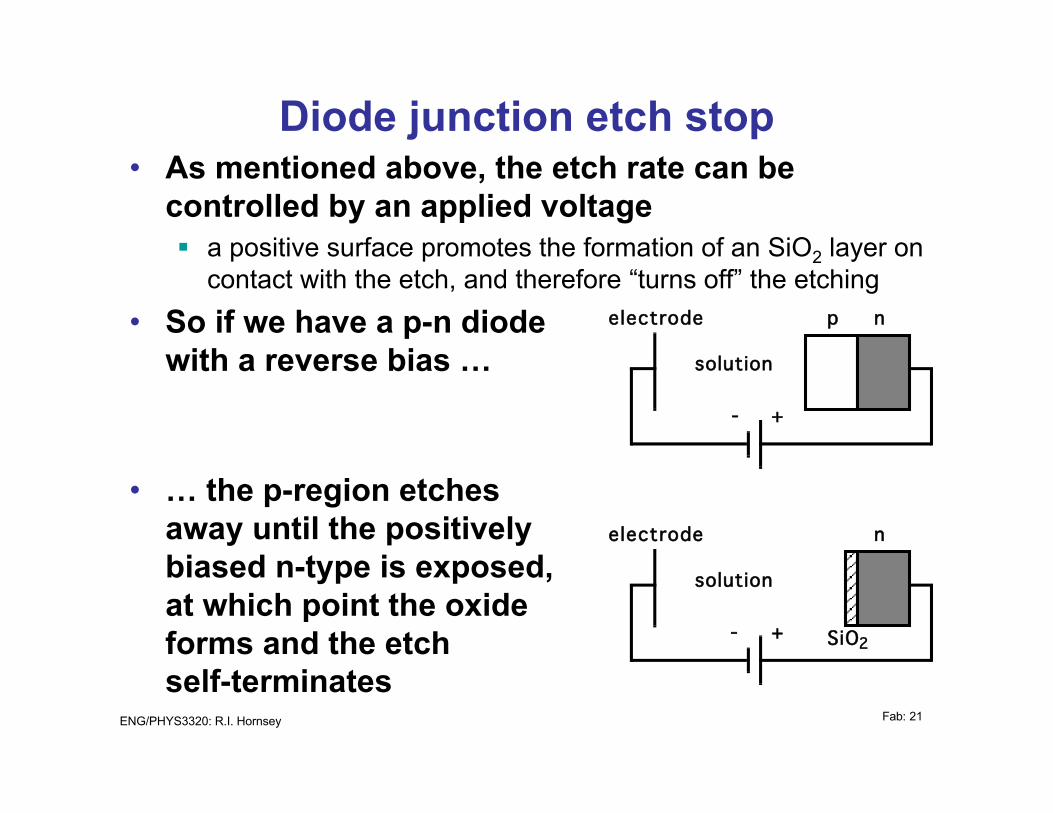
Diode junction etch stop• As mentioned above, the etch rate can be
controlled by an applied voltageß a positive surface promotes the formation of an SiO2 layer on
contact with the etch, and therefore “turns off” the etching
• So if we have a p-n diodewith a reverse bias …
• … the p-region etchesaway until the positivelybiased n-type is exposed,at which point the oxideforms and the etchself-terminates
n
solution
- +
electrode p
n
solution
- +
electrode
SiO2
ENG/PHYS3320: R.I. Hornsey Fab: 22
Dry etching• While wet etching has many advantages …ß chemical cost, equipment cost, speed
• … it can be hard to control and relativelyinflexible
• There is also a limit on the achievable aspectratioß especially for (100) CMOS because the anisotropy results
from the crystal planes – vertical walls are not possible.
• Dry etching is a class of etching that does notrely on wet chemicals but on ion bombardment to“sputter” away a surface
ENG/PHYS3320: R.I. Hornsey Fab: 23
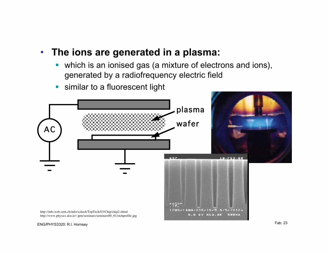
• The ions are generated in a plasma:ß which is an ionised gas (a mixture of electrons and ions),
generated by a radiofrequency electric field
ß similar to a fluorescent light
AC
plasma
wafer
http://info.web.cern.ch/info/scitech/TopTech/03/Chip/chip2.shtmlhttp://www.physics.dcu.ie/~jpm/seminars/seminars00_01/etchprofile.jpg
ENG/PHYS3320: R.I. Hornsey Fab: 24
• Between the plasma and the wafer is a regionwhere the electric field is perpendicular to thewaferß and which accelerates the positive ions from the plasma
towards the wafer
• The impact of the ions removes the wafermaterial at a rate which depends on:ß plasma power
ß plasma ion species
ß target material
• A purely physical etching tends to give morevertical edgesß but the etch rate will likely be low
ß this is sometimes used just to clean surfaces
ENG/PHYS3320: R.I. Hornsey Fab: 25
• While such plasma etching can be a purelyphysical process, with the appropriatecompositions it can also involve chemistryß chemical reactions which would otherwise require very high
temperatures (>1000°C) can take place at <300°C becauseenergy is provided by the plasma
ß [a similar plasma process, called plasma enhanced chemicalvapour deposition, can be used to deposit materials – suchas amorphous silicon – at low temperatures]
• The resulting degree of anisotropy depends onthe ratio of the physical and chemical processes
• This techniques is known as reactive ion etching– RIE
ENG/PHYS3320: R.I. Hornsey Fab: 26
• If the radicals freed in the plasma chemically etchthe substrate without the need for ionbomdardmentß the etching will be isotropic
ß e.g. SF6
• Adding in FREON115 (CClF5) to the SF6 allowscontrol of the lateral etchingß on the side walls, a protective polymer of fluorine-rich
fluorocarbon is deposited which inhibits lateral etching
ß on the bottom, the polymer is both thin and carbon-rich andetches rapidly (>250nm/min)
ß hence a high degree of anisotropy is achieved
• As with the wet etching, the local availability ofthe reactants will affect the profile of the hole
ENG/PHYS3320: R.I. Hornsey Fab: 27
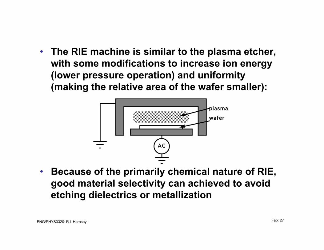
• The RIE machine is similar to the plasma etcher,with some modifications to increase ion energy(lower pressure operation) and uniformity(making the relative area of the wafer smaller):
• Because of the primarily chemical nature of RIE,good material selectivity can achieved to avoidetching dielectrics or metallization
AC
plasma
wafer
ENG/PHYS3320: R.I. Hornsey Fab: 28
• While basic RIE can achieve a reasonableanisotropy, it is not good enough for aspectratios much bigger than 10:1
• Enter Deep Reactive Ion Etching – DRIE
ENG/PHYS3320: R.I. Hornsey Fab: 29
DRIE• In order to enhance the anisotropy (and hence the
maximum depth of hole), the polymerisationprocess described above can be enhanceddeliberately, by alternatingß an etching step (e.g. SF6/Ar)
ß with a polymerisation step (e.g. SF6/C4F4)
ß the polymer is effectively teflon (~50nm), and naturally coatsboth vertical and horizontal surfaces
ß however, adding ion bombardment during polymerisationalmost prevents the teflon formation at the bottom of the hole
• Holes up to 1mm deep, with a 30:1 aspect ratioand an etch rate of 2µm/minute can be achievedß with >100:1 selectivity over SiO2
ENG/PHYS3320: R.I. Hornsey Fab: 30
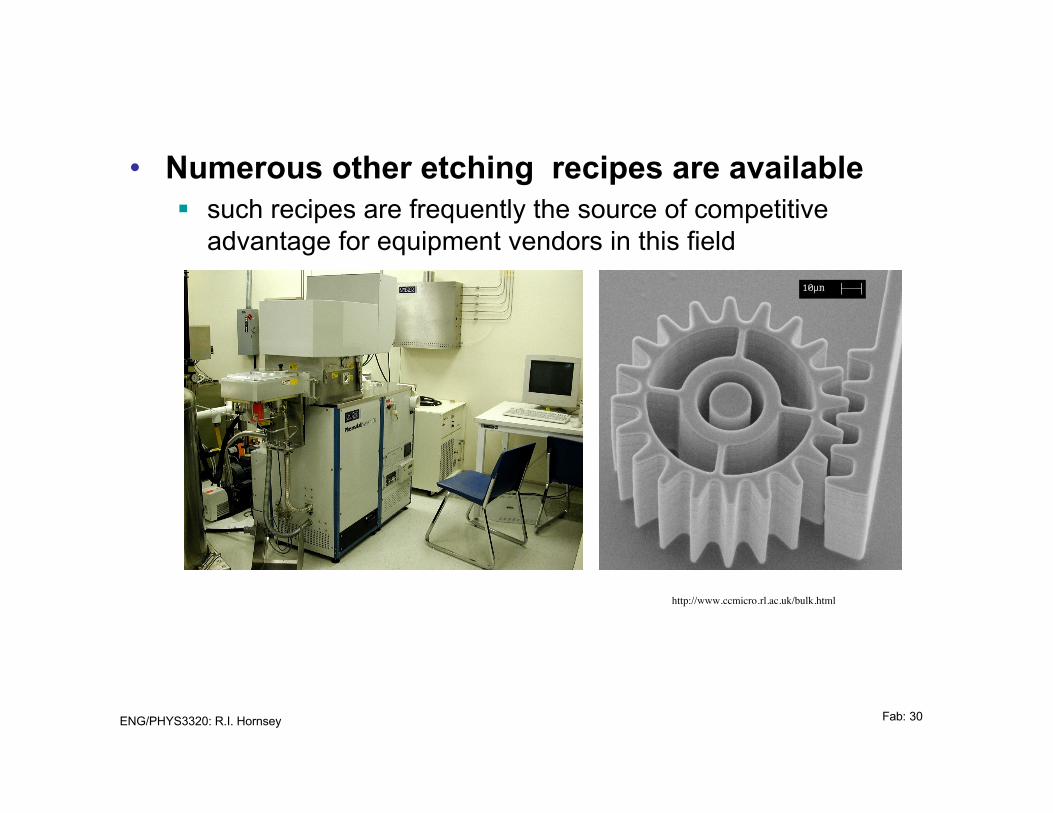
• Numerous other etching recipes are availableß such recipes are frequently the source of competitive
advantage for equipment vendors in this field
http://www.ccmicro.rl.ac.uk/bulk.html
ENG/PHYS3320: R.I. Hornsey Fab: 31
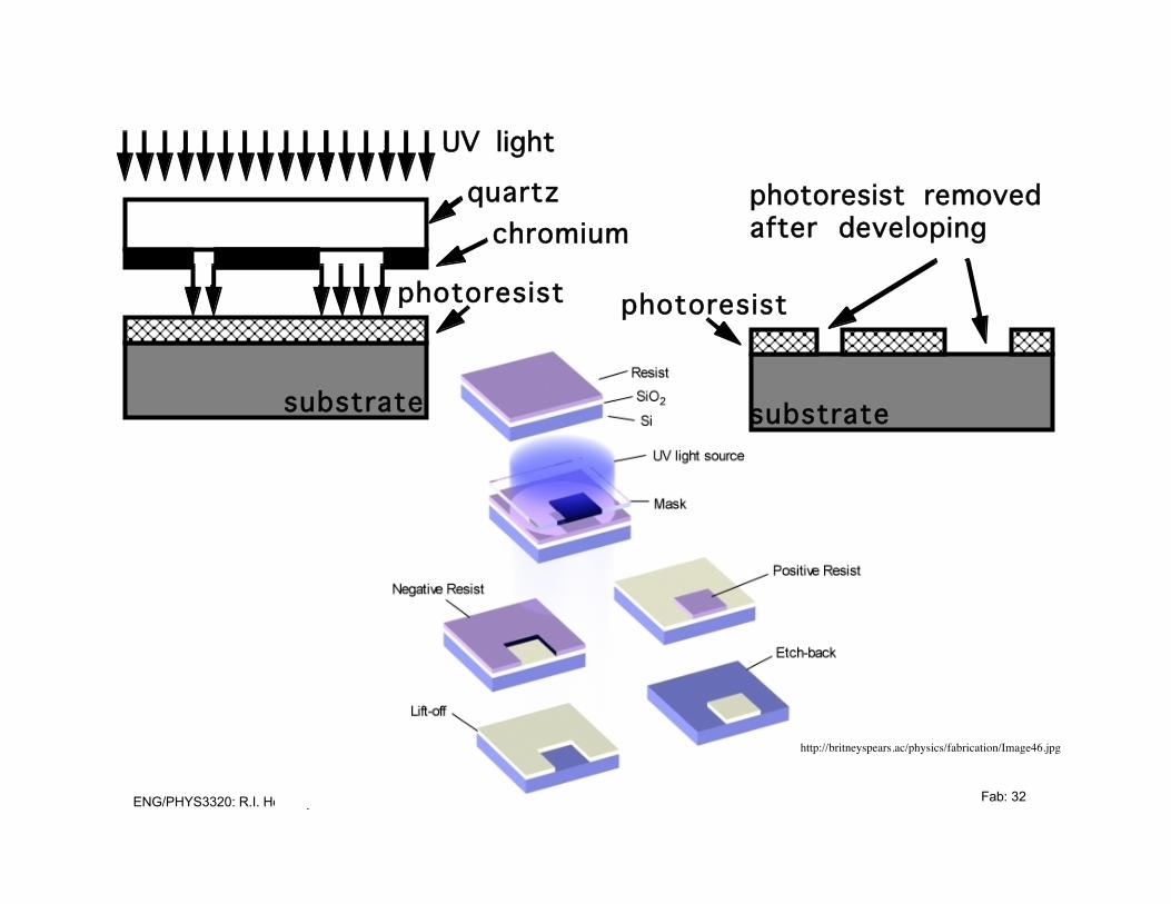
Lithography• Both wet and dry etching techniques are
immersive (as opposed to “direct write”) andhence rely on a patterned masking layer toprotect some areas of the substrate fromundesired etching
• Patterning is transferred to the mask layer by aprocess called photolithographyß photo = light, litho = stone, graphy = writing
• In practice, this is achieved by exposing a light-sensitive chemical (the photoresist) to ultra-violetlight, through an optical maskß the optical mask is typically formed by a set of photographic
reductions from a 100x master pattern
ß and is usually chromium on quartz
ENG/PHYS3320: R.I. Hornsey Fab: 32
photoresist
chromiumquartz
UV light
substrate
photoresist
substrate
photoresist removed after developing
http://britneyspears.ac/physics/fabrication/Image46.jpg
ENG/PHYS3320: R.I. Hornsey Fab: 33
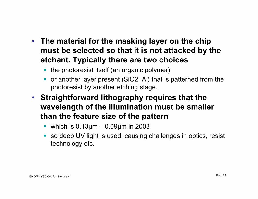
• The material for the masking layer on the chipmust be selected so that it is not attacked by theetchant. Typically there are two choicesß the photoresist itself (an organic polymer)
ß or another layer present (SiO2, Al) that is patterned from thephotoresist by another etching stage.
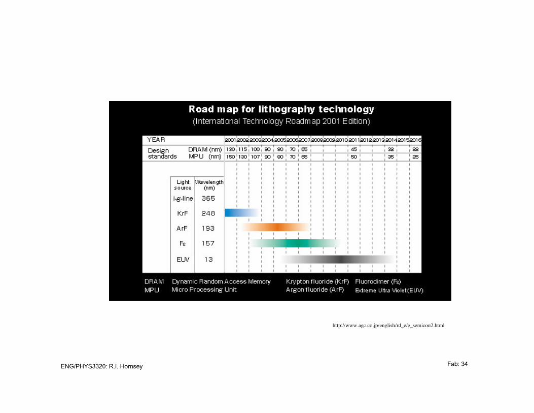
• Straightforward lithography requires that thewavelength of the illumination must be smallerthan the feature size of the patternß which is 0.13µm – 0.09µm in 2003
ß so deep UV light is used, causing challenges in optics, resisttechnology etc.
ENG/PHYS3320: R.I. Hornsey Fab: 34
http://www.agc.co.jp/english/rd_e/e_semicon2.html
ENG/PHYS3320: R.I. Hornsey Fab: 35
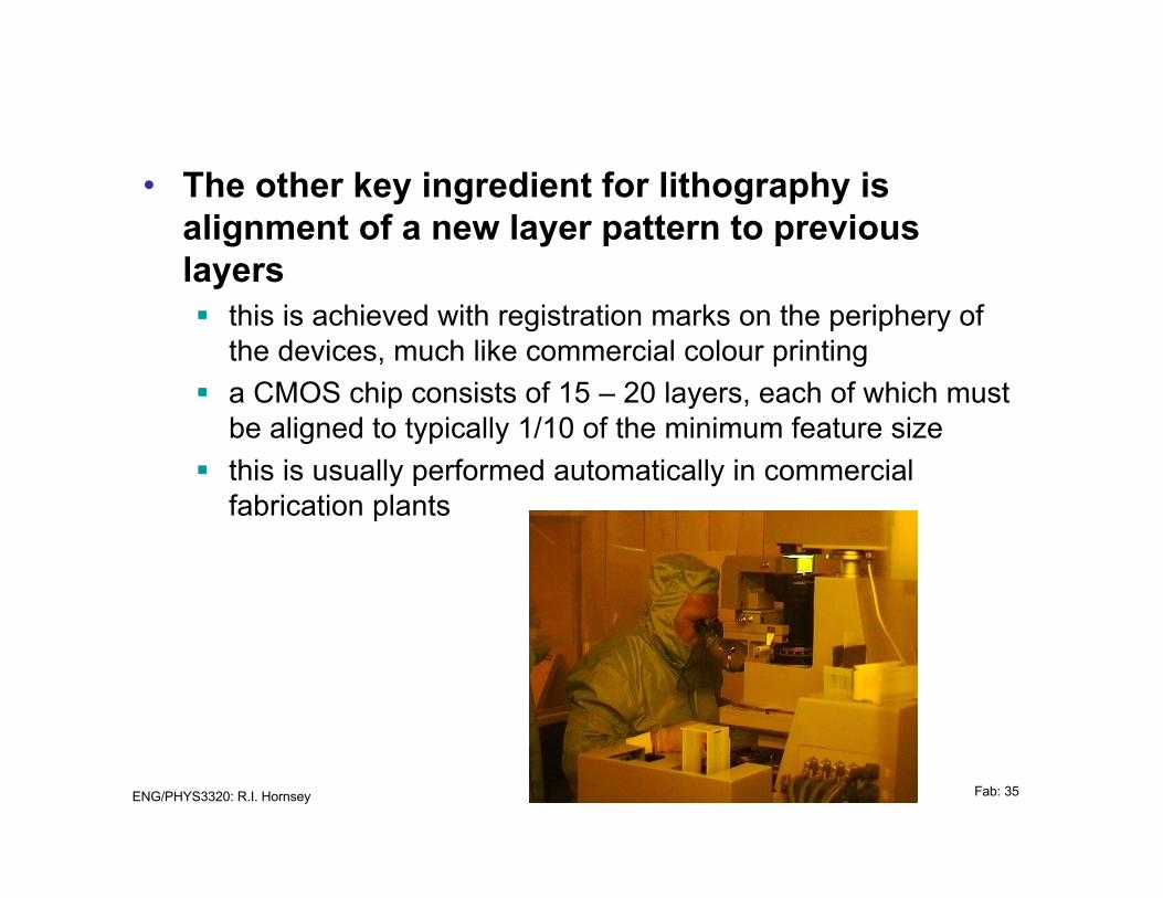
• The other key ingredient for lithography isalignment of a new layer pattern to previouslayersß this is achieved with registration marks on the periphery of
the devices, much like commercial colour printing
ß a CMOS chip consists of 15 – 20 layers, each of which mustbe aligned to typically 1/10 of the minimum feature size
ß this is usually performed automatically in commercialfabrication plants
ENG/PHYS3320: R.I. Hornsey Fab: 36
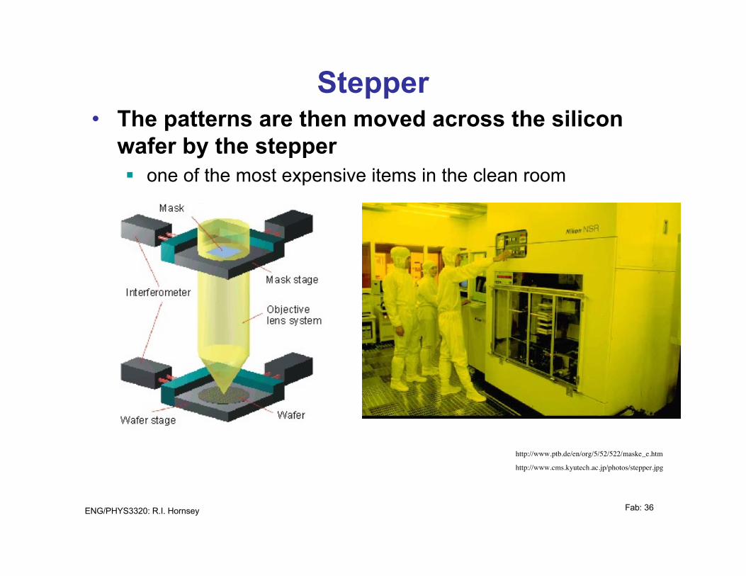
Stepper• The patterns are then moved across the silicon
wafer by the stepperß one of the most expensive items in the clean room
http://www.ptb.de/en/org/5/52/522/maske_e.htm
http://www.cms.kyutech.ac.jp/photos/stepper.jpg
ENG/PHYS3320: R.I. Hornsey Fab: 37
Deposition• Surface micromachining requires prior deposition
of layers, which can then be selectively etchedß i.e. “additive” processes
• Layer structures needed for MEMS are notusually available in the standard CMOS processß and must therefore be deposited subsequently, in a
compatible post-processing stage
ß materials used in MEMS are still counted as “thin” films,even though they may be 10–100 times thicker than those inCMOS
ENG/PHYS3320: R.I. Hornsey Fab: 38
• Compatible means that:ß deposition temperature is low (<350°C because of Al
metallization)
ß low stress/strain in films (to avoid distortion)
ß good coverage of “steps”
ß good uniformity and integrity
ß good properties for micromachining
• Two broad categories:
• Non-metallic thin film depositionß such as SiO2, poly-Si, silicon nitrides (SixNy)
• Metallic thin film depositionß Al, Au, Cu
ENG/PHYS3320: R.I. Hornsey Fab: 39
Silicon dioxide• SiO2 can be obtained (grown or deposited) in
several ways:ß thermal growth from Si
ß deposited (see below)
ß phosphorus-doped = phosphosilicate glass (PSG), used asfinal coating on chips
ß boron-doped = borosilicate glass (BSG)
ß both P- and B-doped = BPSG, or low-temperature oxide(LTO)
• LTO is useful because it flows well at lowtemperatures, and smooths out the underlyingsurface (called planarization)
ENG/PHYS3320: R.I. Hornsey Fab: 40
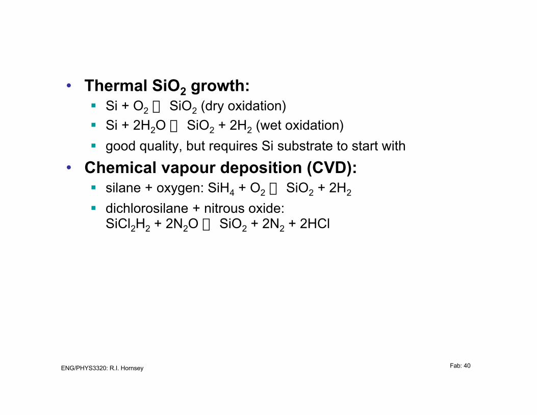
• Thermal SiO2 growth:ß Si + O2 Æ SiO2 (dry oxidation)
ß Si + 2H2O Æ SiO2 + 2H2 (wet oxidation)
ß good quality, but requires Si substrate to start with
• Chemical vapour deposition (CVD):ß silane + oxygen: SiH4 + O2 Æ SiO2 + 2H2
ß dichlorosilane + nitrous oxide:SiCl2H2 + 2N2O Æ SiO2 + 2N2 + 2HCl
ENG/PHYS3320: R.I. Hornsey Fab: 41
Kovacs, p.79
ENG/PHYS3320: R.I. Hornsey Fab: 42
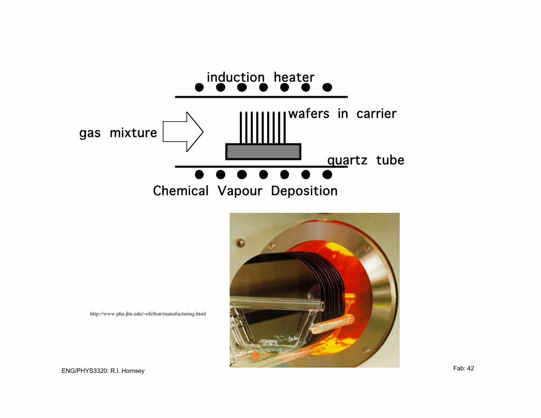
http://www.pha.jhu.edu/~efelton/manufacturing.html
gas mixture
induction heater
wafers in carrier
quartz tube
Chemical Vapour Deposition
ENG/PHYS3320: R.I. Hornsey Fab: 43
• Both the thermal growth and the CVD aboverequire high temperatures (~1000°C) to achievedecomposition of the appropriate materialsß these are therefore not CMOS-compatible
• Plasma-enhanced CVD (PECVD) is morecommonly used, because:ß low temperature
ß control of stress is possible by adjusting plasma conditions
ß similar to the plasma etcher, but conditions are chosen topromote deposition over etching
ENG/PHYS3320: R.I. Hornsey Fab: 44
Silicon Nitride• SiN has many useful properties for MEMS:ß structural material
ß passivation (protective) layer
ß mask for etching/oxidation of Si
ß dielectric material
• It also has a different dielectric constant fromSiO2 which gives it useful optical propertiesß anti-reflective coating, waveguide
• The “normal” (stoichiometric) composition ofsilicon nitride is Si3N4
ß but other stoichiometries can be used (i.e. silicon-rich ornitrogen-rich)
ß which have different properties, especially with regard tostress.
ENG/PHYS3320: R.I. Hornsey Fab: 45
• A common CVD reaction for SiN isß 3SiH4 + 4NH3 Æ Si3N4 + 12H2
• Or, for PECVD:ß SiH4 + NH3 Æ SiNH + 3H2
• In the PECVD case, the presence of the hydrogenaffects the stoichiometry. This in turn is affectedby the plasma power and frequencyß which in turn affects the stressß e.g. 13.56MHz Æ 400MPa tensile stress
ß while 50kHz Æ 200MPa compressive stress
ß [atmospheric pressure is 0.1MPa]
ENG/PHYS3320: R.I. Hornsey Fab: 46
Polysilicon• The main use of poly in MEMS is as a structural
material
• In CMOS it forms the gates of MOSFETs andshort interconnectsß and is deposited at high (600°C) using CVD
• Poly can also be deposited using PECVD (dopedor undoped), where the temperature determinesthe morphology of the film:ß T>~350°C Æ poly
ß T ≈ 250°C Æ amorphous
ENG/PHYS3320: R.I. Hornsey Fab: 47
Deposition of metallic thin films• Metallic films for ICs and micromachining are
deposited primarily in four waysß evaporation – either resistive heating or electron beam
ß sputtering
ß electrodeposition
• The choice of technique depends on the metal,the deposition rate and the morphology required
ENG/PHYS3320: R.I. Hornsey Fab: 48
Thermal evaporation• hermal evaporation is the workhorse of
deposition processes because it is simple, cheap,and reasonable quality
• Deposition by evaporation is simply anevaporation/condensation processß the metal is heated until it evaporates
ß the neutral atomic flux is then condensed onto the coolersubstrate
ß sometimes the metal to be deposited is wound around aheater filament (if a higher temperature is needed)
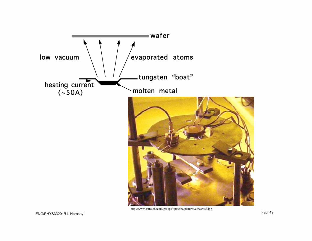
ENG/PHYS3320: R.I. Hornsey Fab: 49http://www.astro.cf.ac.uk/groups/optoelec/pictures/edwards2.jpg
heating current (~50A)
wafer
evaporated atoms
tungsten “boat”
molten metal
low vacuum
ENG/PHYS3320: R.I. Hornsey Fab: 50
• Resistive heating is limited by the temperature towhich the boat/filament can be heated (~1400°Cfor W)ß so it is good for Al, Au, Mg, Cr
• Evaporation may not be good for depositingalloysß because the various constituents may not evaporate at the
same rate, and the deposited film may have a differentcomposition than the original metal
• Film uniformity depends on the ratio of the wafersize to the boat-wafer separationß increasing the separation to cope with larger wafers also
requires higher vacuum to give the metal atoms a highermean free path
ENG/PHYS3320: R.I. Hornsey Fab: 51
• The nature of the deposited film depends on thetemperature of the substrateß the temperature determines the mobility of the adsorbed
atoms on the surface
ß the more rearrangement they are allowed, the more likeepitaxy the process becomes, and the less stress there is inthe film
ß in general, the nearer the substrate temperature to themelting point of the deposited metal, the lower the stress
ß so lower melting point metals (Al, Au) have lower stress
• Deposition rates are typically ~nm/s
ENG/PHYS3320: R.I. Hornsey Fab: 52
Electron beam evaporation• In order to escape from the heating limitations of
resistive heating, the metal can be evaporated byelectron beam bombardmentß 10keV @ 100mA, leading to 1kW/mm3 density
• This method both allows other materials (e.g. Ti,Pt, W) to be deposited with a higher rateß the source temperature may get to 3000°C if the target wafer
can be cooled sufficiently
ß rate ~100nm/s
• One of the disadvantages of electron beamevaporation is the generation of x-raysß indeed, this is how x-rays are normally generated!
ß so appropriate shielding, both of the operator and of thewafer, is required
ENG/PHYS3320: R.I. Hornsey Fab: 53
Sputter deposition• Sputter deposition is the other very common
metal deposition techniqueß and is a cross between plasma etching and evaporation
• Now, instead of removing atoms from the sourcemetal by evaporation, they are removed by ionbombardment (= sputtering) from a plasmaß typically the plasma is argon (Ar+) because it causes little
contamination
• Because the metal atoms are actively “knockedoff”, they are more energeticß and hence have a higher surface mobility
ß stress control is therefore better, as well as better stepcoverage
ENG/PHYS3320: R.I. Hornsey Fab: 54
• Moreover, the sputtering yield of different metalsdoes not vary widely, so alloys are sputtered withthe same stoichiometry as the source metal
• The type of plasma source has an influence,particularly because higher power sources areneeded to sputter harder metals
• DC plasmas are able to sputter soft metalsß but if we want higher powers or to sputter dielectrics, we
need an AC plasma
ß this is to avoid charging of the insulating target
ß typically, RF plasmas at 13.56MHz are used
• Sputtered metal films tend to be under tensilestress
ENG/PHYS3320: R.I. Hornsey Fab: 55
• Care must be taken to cool the wafer (it heats dueto secondary electrons emitted from the target)ß and there will be a small amount of residual incorporation of
the plasma material in the deposited film
ENG/PHYS3320: R.I. Hornsey Fab: 56
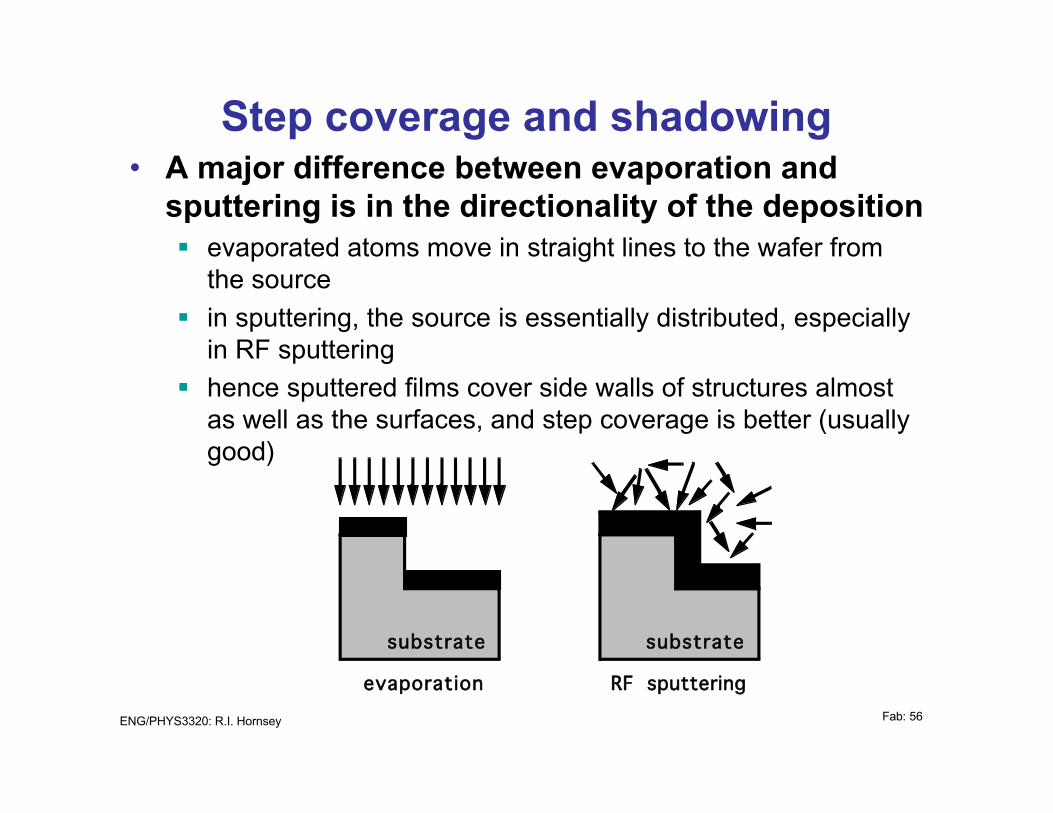
Step coverage and shadowing• A major difference between evaporation and
sputtering is in the directionality of the depositionß evaporated atoms move in straight lines to the wafer from
the source
ß in sputtering, the source is essentially distributed, especiallyin RF sputtering
ß hence sputtered films cover side walls of structures almostas well as the surfaces, and step coverage is better (usuallygood)
substrate substrate
evaporation RF sputtering
ENG/PHYS3320: R.I. Hornsey Fab: 57
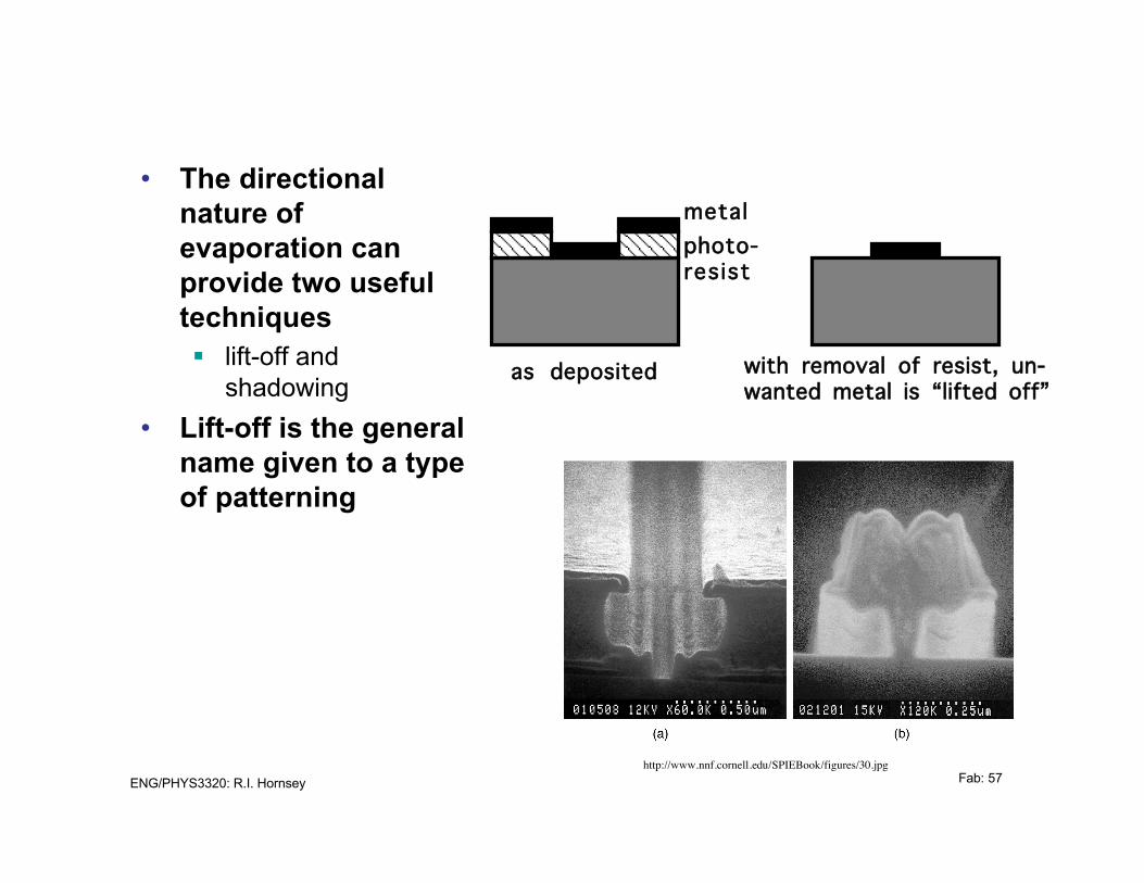
• The directionalnature ofevaporation canprovide two usefultechniquesß lift-off and
shadowing
• Lift-off is the generalname given to a typeof patterning
http://www.nnf.cornell.edu/SPIEBook/figures/30.jpg
metalphoto-resist
as deposited with removal of resist, un-wanted metal is “lifted off”
ENG/PHYS3320: R.I. Hornsey Fab: 58
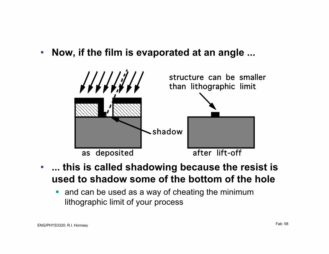
• Now, if the film is evaporated at an angle ...
• ... this is called shadowing because the resist isused to shadow some of the bottom of the holeß and can be used as a way of cheating the minimum
lithographic limit of your process
after lift-off
structure can be smaller than lithographic limit
as deposited
shadow
ENG/PHYS3320: R.I. Hornsey Fab: 59
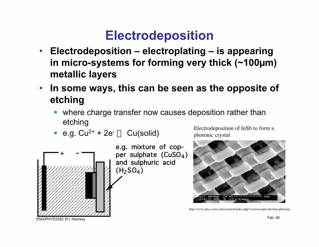
Electrodeposition• Electrodeposition – electroplating – is appearing
in micro-systems for forming very thick (~100µm)metallic layers
• In some ways, this can be seen as the opposite ofetchingß where charge transfer now causes deposition rather than
etchingß e.g. Cu2+ + 2e- Æ Cu(solid)
–+e.g. mixture of cop-per sulphate (CuSO4) and sulphuric acid (H2SO4)
http://www.phys.cwru.edu/research/index.php?section=optics&what=photonic
Electrodeposition of InSb to form aphotonic crystal
ENG/PHYS3320: R.I. Hornsey Fab: 60
ß a conducting template layer is formed first by e.g.evaporation to form the base for the electrodeposition
ß but this template is not usually sufficient to define the wholestructure because the electrodeposition does not formvertical edges (see next section)
• Common materials to be electrodeposited are Au,Ag, Cu, Ni, Ptß such processes have been in use for ~100 years and many
recipes are well known
• Gold is deposited from gold cyanide, e.g.ß Au(CN)2- ´ AuCN + CN- and AuCN + e- Æ Au(s) + CN-
• As with anisotropic etching, the deposition rate isdependent on the crystal plane
ENG/PHYS3320: R.I. Hornsey Fab: 61
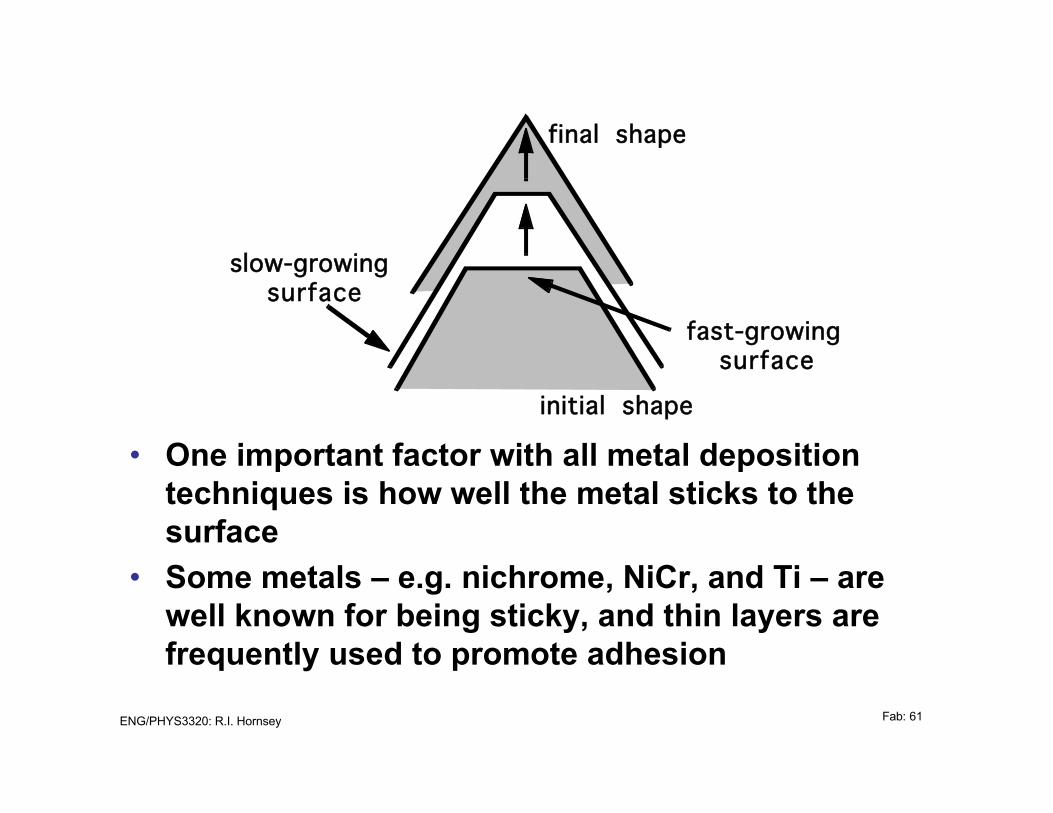
• One important factor with all metal depositiontechniques is how well the metal sticks to thesurface
• Some metals – e.g. nichrome, NiCr, and Ti – arewell known for being sticky, and thin layers arefrequently used to promote adhesion
fast-growing surface
slow-growing surface
final shape
initial shape
ENG/PHYS3320: R.I. Hornsey Fab: 62
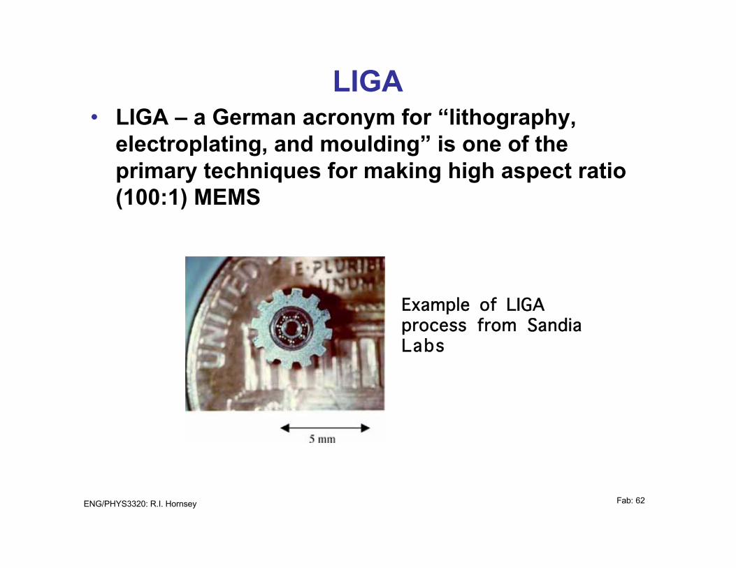
LIGA• LIGA – a German acronym for “lithography,
electroplating, and moulding” is one of theprimary techniques for making high aspect ratio(100:1) MEMS
Example of LIGA process from Sandia Labs
ENG/PHYS3320: R.I. Hornsey Fab: 63
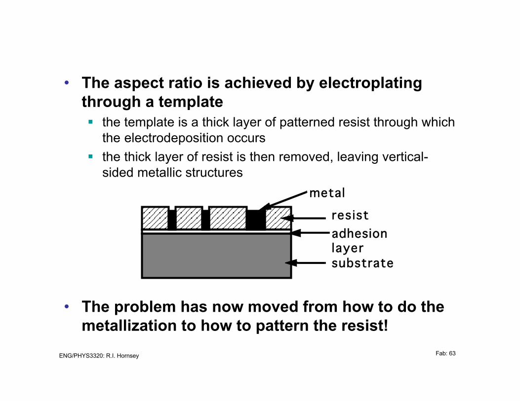
• The aspect ratio is achieved by electroplatingthrough a templateß the template is a thick layer of patterned resist through which
the electrodeposition occurs
ß the thick layer of resist is then removed, leaving vertical-sided metallic structures
• The problem has now moved from how to do themetallization to how to pattern the resist!
resist
metal
adhesionlayersubstrate
ENG/PHYS3320: R.I. Hornsey Fab: 64
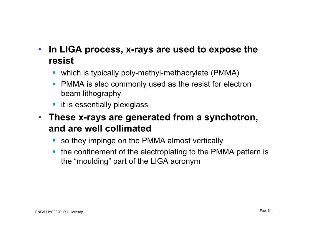
• In LIGA process, x-rays are used to expose theresistß which is typically poly-methyl-methacrylate (PMMA)
ß PMMA is also commonly used as the resist for electronbeam lithography
ß it is essentially plexiglass
• These x-rays are generated from a synchotron,and are well collimatedß so they impinge on the PMMA almost vertically
ß the confinement of the electroplating to the PMMA pattern isthe “moulding” part of the LIGA acronym
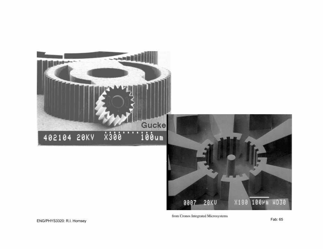
ENG/PHYS3320: R.I. Hornsey Fab: 65from Cronos Integrated Microsystems
ENG/PHYS3320: R.I. Hornsey Fab: 66
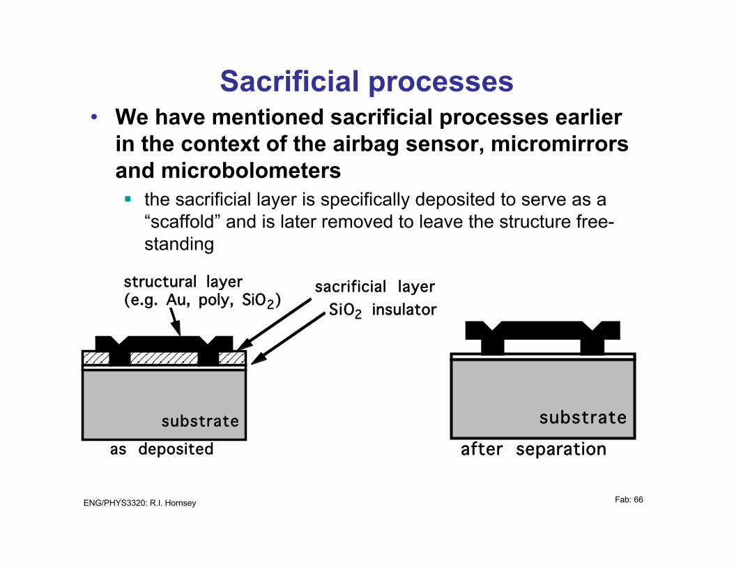
Sacrificial processes• We have mentioned sacrificial processes earlier
in the context of the airbag sensor, micromirrorsand microbolometersß the sacrificial layer is specifically deposited to serve as a
“scaffold” and is later removed to leave the structure free-standing
substrate
structural layer (e.g. Au, poly, SiO2) SiO2 insulator
sacrificial layer
as deposited
substrate
after separation
ENG/PHYS3320: R.I. Hornsey Fab: 67
• Sacrificial layers can be resists, phosphosilicateglass (PSG), oxide, nitrideß the sacrificial layer should etch much faster than the
structural layer
• If the structure to be released has a large area,care must be taken to ensure that the sacrificiallayer is exposed adequately to the etchantß otherwise the etch time will be so long that the structure may
also be damaged
ß this is frequently achieved simply by forming holes in thestructure to allow the etchant underneath
ENG/PHYS3320: R.I. Hornsey Fab: 68
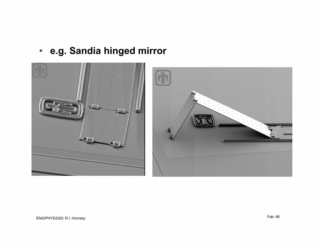
• e.g. Sandia hinged mirror
ENG/PHYS3320: R.I. Hornsey Fab: 69
http://www.imt.tu-bs.de/mitarbeiter/seidemann/projekte/SU8compliant_struc.htm
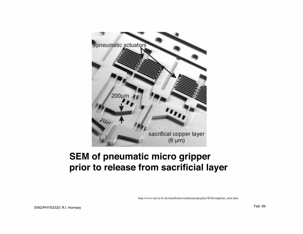
SEM of pneumatic micro gripperprior to release from sacrificial layer
ENG/PHYS3320: R.I. Hornsey Fab: 70
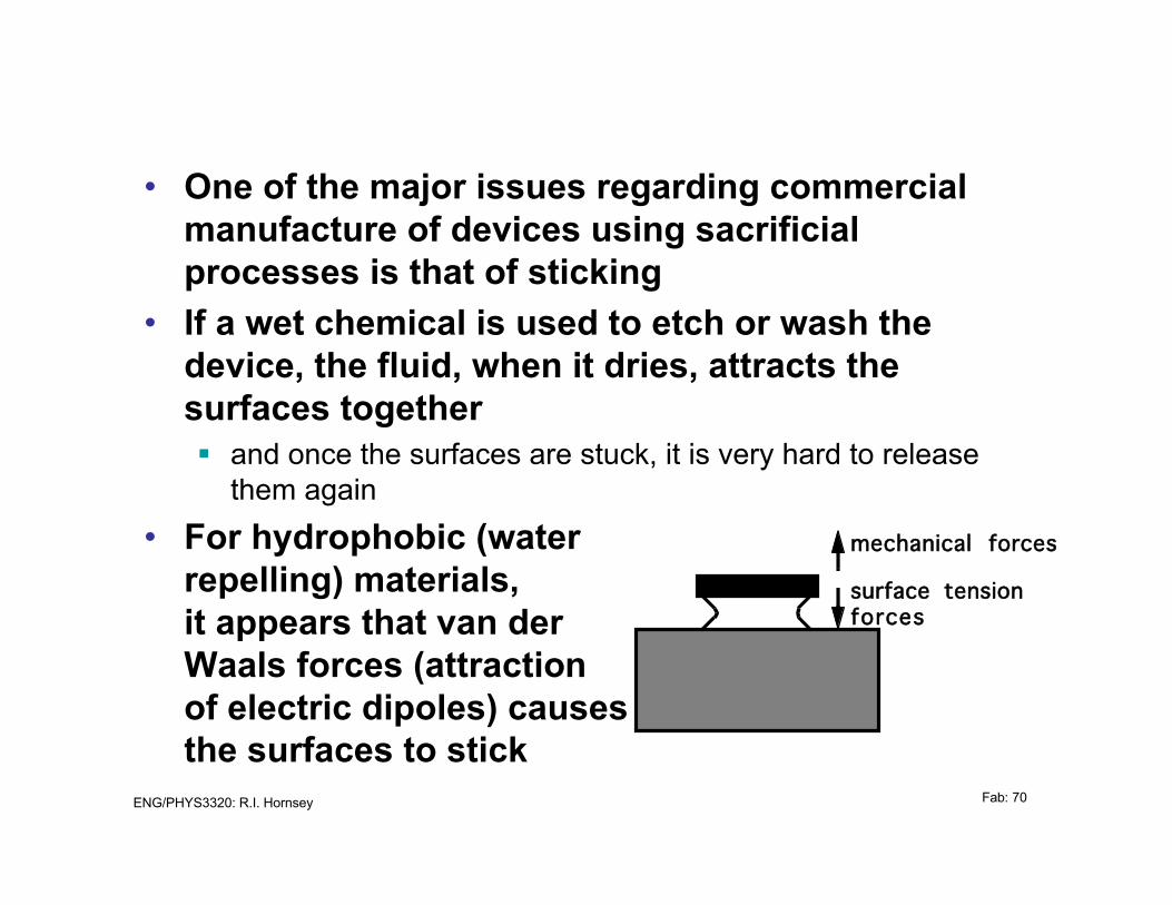
• One of the major issues regarding commercialmanufacture of devices using sacrificialprocesses is that of sticking
• If a wet chemical is used to etch or wash thedevice, the fluid, when it dries, attracts thesurfaces togetherß and once the surfaces are stuck, it is very hard to release
them again
• For hydrophobic (waterrepelling) materials,it appears that van derWaals forces (attractionof electric dipoles) causesthe surfaces to stick
mechanical forces
surface tension forces
ENG/PHYS3320: R.I. Hornsey Fab: 71
• For hydrophilic (water attracting) materials,hydrogen bonding (bonding of surface OHgroups) is responsibleß silicon falls into this group
• The typical technique for avoiding this problem isto avoid the liquid drying phase byß first freezing the liquid (e.g. butyl alcohol)
ß then the solid is sublimed (solid goes straight to gas) in avacuum
ß this is the same process used for freeze drying foods
ENG/PHYS3320: R.I. Hornsey Fab: 72
Conclusion• This chapter has provided an overview of the
basic micromachining, and other, fabricationtechniques relevant to a range of microsystems
• We will come across other fabrication issues aswe discuss specific transducers
• We have discussed subtractive and additiveprocesses, lithographyß we have not yet talked much about materials properties, but
these too are important
• With these ideas of fabrication in our minds, wecan now progress to individual transductionmechanisms, and examples of practicalimplementations