Embed Size (px)
Citation preview
Advanced Search
English : Support : 54355
AR# 54355 Virtex-7 FPGA VC709 Connectivity Kit - Board Debug Checklist
Description Solution Linked Answer Records
Description
The VC709 Connectivity Kit Board Debug Checklist is useful to debug board-related issues and to determine if requesting a Boards RMA is the next step.
Before working through the VC709 Board Debug Checklist, please review (Xilinx Answer 51901) Virtex-7 FPGA VC709 Connectivity Kit - Known Issues and Release Notes Master Answer Record.
Solution
Sign In Documentation Downloads Contact Us Shopping Cart (0)Language
Products Applications Support Buy About Xilinx
Page 1 of 1554355
4/9/2013http://www.xilinx.com/support/answers/54355.html
54355-1.jpg
1. Switch / Jumper Settings2. Board Power3. Cable detection4. JTAG Initialization
The following debug steps assume steps 1-4 have been checked and are working:5. JTAG Configuration6. BPI Configuration7. XADC8. PCIe9. IBERT10. DDR311. Interface Tests12. Known Issues for VC709
1. Switch / Jumper Settings
Default Switch and Jumper Settings for the VC709 are:
Start from a known safe scenario by verifying the default Switch and Jumper settings. You can then set switches / jumpers for your application.
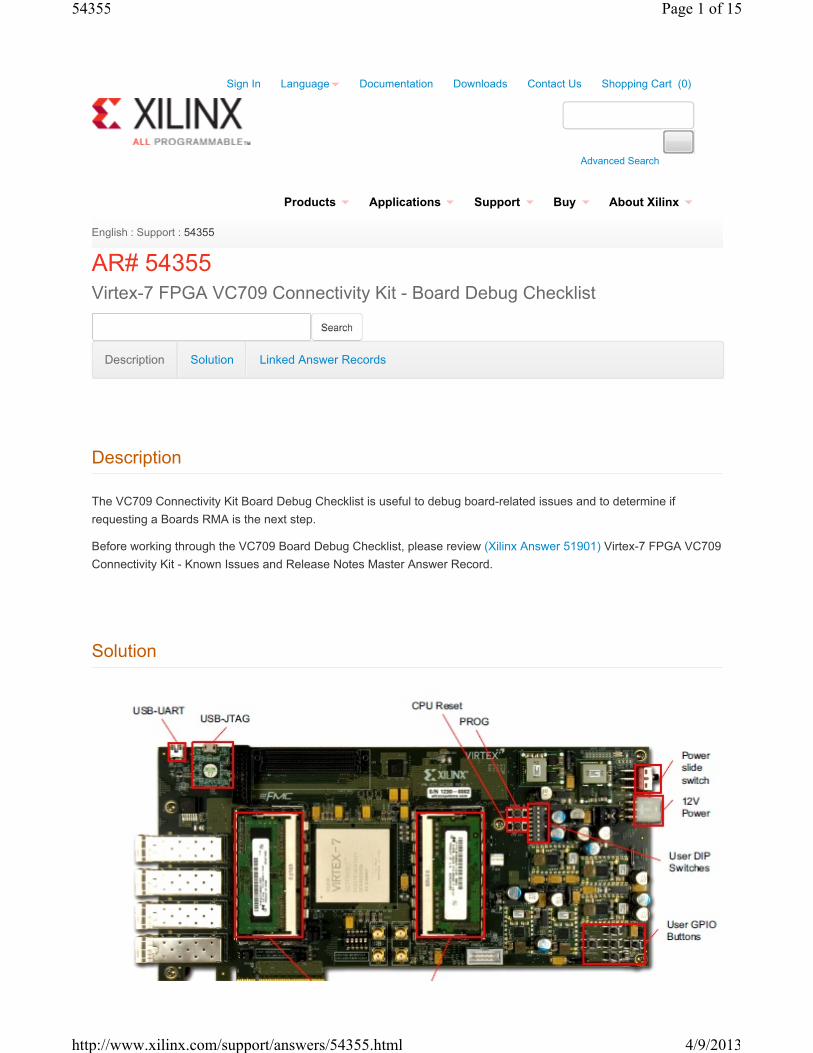
a. GPIO DIP Switch SW2
54355-2.jpg
Page 2 of 1554355
4/9/2013http://www.xilinx.com/support/answers/54355.html
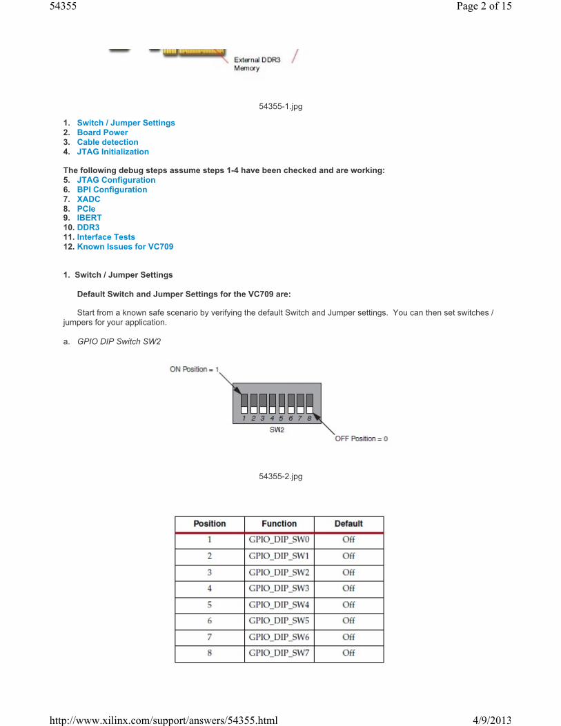
54355-3.jpg
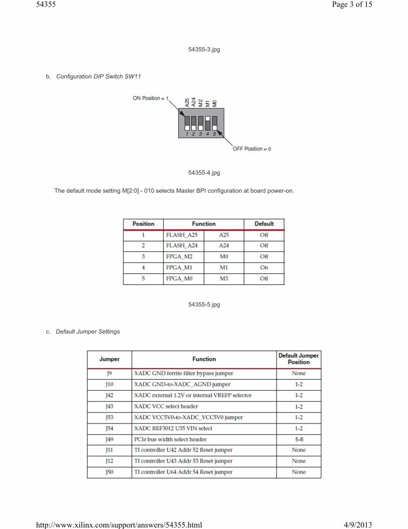
b. Configuration DIP Switch SW11
54355-4.jpg
The default mode setting M[2:0] - 010 selects Master BPI configuration at board power-on.
54355-5.jpg
c. Default Jumper Settings
Page 3 of 1554355
4/9/2013http://www.xilinx.com/support/answers/54355.html
54355-6.jpg
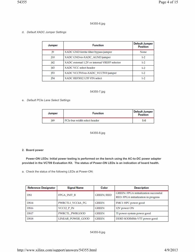
d. Default XADC Jumper Settings
54355-7.jpg
e. Default PCIe Lane Select Settings
54355-8.jpg
2. Board power
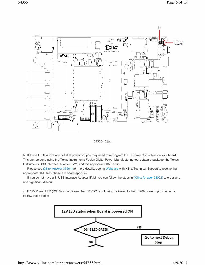
Power-ON LEDs: Initial power testing is performed on the bench using the AC-to-DC power adapter provided in the VC709 Evaluation Kit. The status of Power-ON LEDs is an indication of board health.
a. Check the status of the following LEDs at Power-ON:
54355-9.jpg
Page 4 of 1554355
4/9/2013http://www.xilinx.com/support/answers/54355.html
54355-10.jpg
b. If these LEDs above are not lit at power on, you may need to reprogram the TI Power Controllers on your board. This can be done using the Texas Instruments Fusion Digital Power Manufacturing tool software package, the Texas Instruments USB Interface Adapter EVM, and the appropriate XML script. Please see (Xilinx Answer 37561) for more details; open a Webcase with Xilinx Technical Support to receive the appropriate XML files (these are board-specific). If you do not have a TI USB Interface Adapter EVM, you can follow the steps in (Xilinx Answer 54022) to order one at a significant discount.
c. If 12V Power LED (DS16) is not Green, then 12VDC is not being delivered to the VC709 power input connector. Follow these steps:
Page 5 of 1554355
4/9/2013http://www.xilinx.com/support/answers/54355.html

54355-11.jpg
3. Cable detection
The VC709 uses a USB A-to-micro-B cable, plugged into the VC709 Digilent USB-to-JTAG module, U26.
USB A-to-micro-B cablei. Is the cable visible in Device Manager? If the three items highlighted in the figure below are visible in Device Manager, this confirms that your USB cable is operational and has been correctly identified.
Page 6 of 1554355
4/9/2013http://www.xilinx.com/support/answers/54355.html

51233-18.jpg
ii. Are cable drivers loaded correctly? Drivers for this cable should be included in the iMPACT installation. However, if problems are experienced with USB A-to-micro-B cable connection, a Digilent plug-in can be downloaded from the link below. For installation, please follow the guidelines in the document provided in the downloaded files: http://digilentinc.com/Products/Detail.cfm?NavPath=2,66,768&Prod=DIGILENT-PLUGIN.
This plug-in requires Adept systems 2.4 or later for Windows and Adept system 2.3.9 or later for Linux. Adept software is available from Digilent: http://digilentinc.com/Products/Detail.cfm?NavPath=2,66,828&Prod=ADEPT2.iii. Check system properties & environment variables. For information on environment variables, please see (Xilinx Answer 11630).iv. Is the USB port enabled? User can reboot their system to re-initialize the USB buses.v. Are Xilinx tools correctly installed? (iMPACT or ChipScope Pro) (For supported SW version information, please see Kit Product page: VC709)
If an issue is suspected with tools installation, please see Installation and Licensing Guide (make sure to use the most recent version of tools, and associated documentation, which supports the VC709)vi. Is the Operating System (OS) being used Windows 7? If so, please see (Xilinx Answer 41442) and (Xilinx Answer 44397).
If the above steps fail to enable you to connect, please open a Webcase to further debug the problem. In the Webcase notes, please include all debug steps taken to date.
4. JTAG Initialization
The status of the board JTAG chain is checked using Xilinx Tools (iMPACT or ChipScope Pro). To check to see that JTAG chain is initialized correctly, follow this JTAG initialization Test Case:
a. Remove any FMC cards from VC709 b. Set mode switch SW11 for JTAG mode (101) c. Power up VC709 on the bench (not in a PC chassis) d. Connect the Digilent USB A-to-micro-B cable to the VC709 e. Check Digilent device shows up in Device Manager. If not, try a different USB port on your machine. If still unsuccessful, and another USB cable is available to you, try this cable. f. Ensure Xilinx tools (Vivado 2012.4 or later) are correctly installed g. Launch iMPACT - is the cable identified correctly? i. If not, see section 3. Cable detection above. ii. If yes, but iMPACT did not discover and display the JTAG chain, slow down the cable speed (Output > Cable Setup)
iii. If yes, but iMPACT did not discover and display the JTAG chain, and slowing down the cable speed does not resolve the issue, see the following (assumes Digilent USB A-to-micro-B cable is plugged into USB-to-JTAG
Page 7 of 1554355
4/9/2013http://www.xilinx.com/support/answers/54355.html

configuration logic module (U26):
54355-12.jpg
If the above steps fail to enable you to initialize the JTAG chain, please open a Webcase to further debug the problem. In the Webcase notes, please include all debug steps taken to date.
5. JTAG Configuration
JTAG configuration is provided solely through a Digilent onboard USB-to-JTAG configuration logic module (U26)
Page 8 of 1554355
4/9/2013http://www.xilinx.com/support/answers/54355.html

where a host computer accesses the VC709 board JTAG chain through a type-A (host side) to micro-B (VC709 board side) USB cable. If JTAG chain initializes OK, but JTAG configuration fails, check the following:
a. Verify the mode switch settings for JTAG configuration mode:
54355-13.jpg
b. In iMPACT, select a lower cable frequency (Output > Cable Setup) and re-attempt configuration.c. In iMPACT, run the Chain Integrity test by selecting Debug > Chain Integrity Test. iMPACT will assist in the debugging of this scenario by providing insight into where the failing connection in the chain could be.d. Pulse the PROG push button on the VC709 (SW9). Pulsing PROG will clear out any problems caused by power up ramp rate issues to the FPGA.e. Read back the Status Register in iMPACT (Debug > Read Status Register). The information extracted from the Status Register can help determine the stage of configuration and where a failure has occurred. See (Xilinx Answer 24024) for more details.f. Review (Xilinx Answer 34904) - Xilinx Configuration Solution Center. The Configuration Solution Center is available to address all questions related to Configuration.
If the above steps fail to enable JTAG configuration, please open a Webcase to further debug the problem. In the Webcase notes, please include all debug steps taken to date.
6. BPI Configuration
The Linear BPI Flash memory (U3) provides 128 MB of nonvolatile storage that can be used for configuration or software storage. If U3 (BPI flash) on the VC709 contains an image (the as-shipped BIST image or a user-programmed image) and the Virtex-7 FPGA does not configure as expected from the BPI flash, then the following points should be checked:
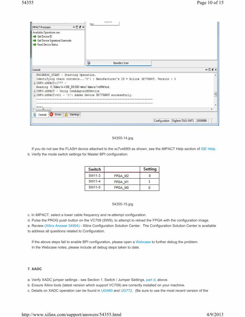
a. If the ".mcs" file is correctly loaded, you will see the FPGA and the FLASH device in the JTAG chain, as shown here:
Page 9 of 1554355
4/9/2013http://www.xilinx.com/support/answers/54355.html
54355-14.jpg
If you do not see the FLASH device attached to the xc7vx690t as shown, see the iMPACT Help section of ISE Help.b. Verify the mode switch settings for Master BPI configuration:
54355-15.jpg
c. In iMPACT, select a lower cable frequency and re-attempt configuration.d. Pulse the PROG push button on the VC709 (SW9), to attempt to reload the FPGA with the configuration image.e. Review (Xilinx Answer 34904) - Xilinx Configuration Solution Center. The Configuration Solution Center is available to address all questions related to Configuration.
If the above steps fail to enable BPI configuration, please open a Webcase to further debug the problem. In the Webcase notes, please include all debug steps taken to date.
7. XADC
a. Verify XADC jumper settings - see Section 1. Switch / Jumper Settings, part d, above.b. Ensure Xilinx tools (latest version which support VC709) are correctly installed on your machine.c. Details on XADC operation can be found in UG480 and UG772. (Be sure to use the most recent version of the
Page 10 of 1554355
4/9/2013http://www.xilinx.com/support/answers/54355.html

document).
If the above steps fail to resolve the XADC issue, please open a Webcase to further debug the problem. In the Webcase notes, please include all debug steps taken to date.
8. PCIe
If the VC709 configures correctly, however the PCIe interface does not operate as expected, check the following:
a. Do NOT plug a PC ATX supply 6-pin connector into J49 on the VC709 board. The ATX 6-pin connector has a different pinout than J49. Connecting an ATX 6-pin connector into J49 will damage the KC705 board and void the board warranty. To install and power the board correctly, follow the instructions given in UG887 VC709 Evaluation Board User Guide - Appendix D - Board Setup. Check J49, lane width, is set correctly.b. Check J49, lane width, is set correctly.c. See (Xilinx Answer 40469) - 7 Series Integrated Block for PCI Express - Release Notes and Known Issues for All Versions affecting PCIe and 7 series, including Virtex-7.d. Download and run the VC709 PCIe Example Design, whichever version is appropriate for your silicon and software version. It is recommended to always use the latest version of software which supports the VC709, and associated version of the VC709 PCIe Example Design. Follow the associated PDF. All are available from the VC709 Example Designs page. VC709 PCIe Design Files: rdf0235.zip VC709 PCIe PDF: xtp237.pdf To identify the silicon version of your kit, please see (Xilinx Answer 37579).e. Read the VC709 PCIe design document: VC709 PCIe PDF: xtp237.pdf (Vivado) and follow the instructions therein.f. Review (Xilinx Answer 34536) - Xilinx Solution Center for PCI Express. The Solution Center for PCI Express is available to address all questions related to the Xilinx solutions for PCI Express
If the above steps fail to resolve the PCIe issue, please open a Webcase to further debug the problem. In the Webcase notes, please include all debug steps taken to date.
9. IBERT
NOTE: Running IBERT requires the installation of ChipScope tool. A device-locked license for this software is provided with the Virtex-7 FPGA VC709 Connectivity kit. If the VC709 configures correctly, however IBERT does not operate as expected, check the following:
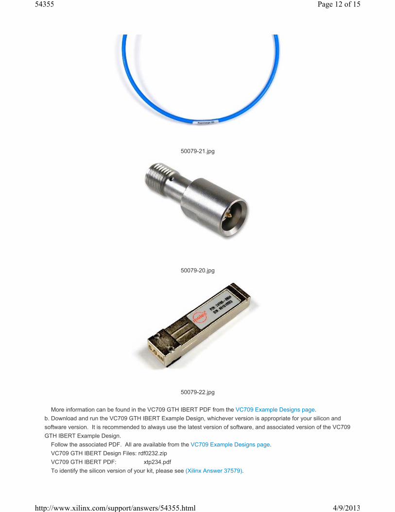
a. If using MGT loopback, ensure you have the correct equipment, including SMA cables, SMA Quick connects and Connect Optical Loopback Adapter:
Page 11 of 1554355
4/9/2013http://www.xilinx.com/support/answers/54355.html
50079-21.jpg
50079-20.jpg
50079-22.jpg
More information can be found in the VC709 GTH IBERT PDF from the VC709 Example Designs page.b. Download and run the VC709 GTH IBERT Example Design, whichever version is appropriate for your silicon and software version. It is recommended to always use the latest version of software, and associated version of the VC709 GTH IBERT Example Design. Follow the associated PDF. All are available from the VC709 Example Designs page. VC709 GTH IBERT Design Files: rdf0232.zip VC709 GTH IBERT PDF: xtp234.pdf To identify the silicon version of your kit, please see (Xilinx Answer 37579).
Page 12 of 1554355
4/9/2013http://www.xilinx.com/support/answers/54355.html

c. Read the VC709 GTH IBERT Example Design document: VC709 GTH IBERT PDF: xtp234.pdf (Vivado) and follow the instructions therein.d. IBERT Design Assistant: (Xilinx Answer 45562).e. Review (Xilinx Answer 45201) - Xilinx ChipScope Solution Center - IBERT Design Assistant. The ChipScope Solution Center is available to address all questions related to ChipScope.
If the above steps fail to resolve the IBERT issue, please open a Webcase to further debug the problem. In the Webcase notes, please include all debug steps taken to date.
10. DDR3
The memory modules at J1 and J3 are 4 GB DDR3 small outline dual-inline memory module (SODIMMs). If a problem is suspected with DDR3 / MIG, check the following:
a. Ensure DDR3 SODIMM module is inserted correctly.b. Download and run the VC709 MIG Example Design, whichever version is appropriate for your silicon and software version. It is recommended to always use the latest version of software which supports the VC709, and associated version of the VC709 MIG Example Design. Follow the associated PDF. All are available from the VC709 Example Design page. VC709 MIG Design Files: rdf0233.zip VC709 MIG PDF: xtp235.pdf To identify the silicon version of your kit, please see (Xilinx Answer 37579).c. Read the VC709 MIG Example Design document: VC709 MIG PDF: xtp235.pdfd. Review (Xilinx Answer 34243) - Xilinx MIG Solution Center. The Memory Interface Generator (MIG) Solution Center is available to address all questions related to MIG.
If the above steps fail to resolve the IBERT issue, please open a Webcase to further debug the problem. In the Webcase notes, please include all debug steps taken to date.
11. Interface Tests
(Xilinx Answer 54568) Virtex-7 FPGA VC709 Connectivity Kit Interface Test Designs can be run to ensure that the interfaces on the VC709 are working correctly. This answer record forms part of (Xilinx Answer 43748) - Boards and Kits Debug Assistant. If the above tests fail to resolve the issue, please open a Webcase to further debug the problem. In the Webcase notes, please include all debug steps taken to date.
12. Known Issues for VC709 All Known Issues for the Virtex-7 FPGA VC709 Connectivity Kit are listed in (Xilinx Answer 51901) Virtex-7 FPGA VC709 Connectivity Kit Known Issues and Release Notes Master Answer Record. If the issue you are faced with is not listed in this Answer Record, and debug fails to resolve the issue, please open a Webcase to further debug the problem. In the Webcase notes, please include all debug steps taken to date.
Page 13 of 1554355
4/9/2013http://www.xilinx.com/support/answers/54355.html
Please Rate this Answer Record
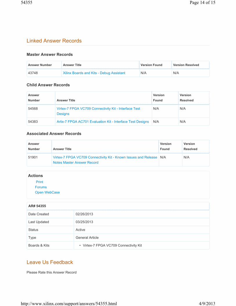
Linked Answer Records
Master Answer Records
Answer Number Answer Title Version Found Version Resolved
43748 Xilinx Boards and Kits - Debug Assistant N/A N/A
Child Answer Records
Answer Number Answer Title
Version Found
Version Resolved
54568 Virtex-7 FPGA VC709 Connectivity Kit - Interface Test Designs
N/A N/A
54383 Artix-7 FPGA AC701 Evaluation Kit - Interface Test Designs N/A N/A
Associated Answer Records
Answer Number Answer Title
Version Found
Version Resolved
51901 Virtex-7 FPGA VC709 Connectivity Kit - Known Issues and Release Notes Master Answer Record
N/A N/A
ActionsPrint ForumsOpen WebCase
AR# 54355
Date Created 02/26/2013
Last Updated 03/25/2013
Status Active
Type General Article
Boards & Kits • Virtex-7 FPGA VC709 Connectivity Kit
Leave Us Feedback
Page 14 of 1554355
4/9/2013http://www.xilinx.com/support/answers/54355.html

Was this Answer Record helpful?
Comments
First Name
Last Name
This answer resolved my issue
This answer did not resolve my issue
Needed additional information to resolve my issue
Provide your email address if you wish to be contacted
Submit Feedback
© Copyright 2013 Xilinx Inc. | Privacy | Trademarks | Legal | Sitemap | Feedback | Contact Us
Page 15 of 1554355
4/9/2013http://www.xilinx.com/support/answers/54355.html


![102 BPI v BPI Employees Union-Davao Chapter [Full Text]](https://img.pdfslide.us/doc/110x75/577cd0261a28ab9e78918703/102-bpi-v-bpi-employees-union-davao-chapter-full-text.jpg)