Embed Size (px)
Citation preview
This journal is© the Owner Societies 2015 Phys. Chem. Chem. Phys., 2015, 17, 13547--13552 | 13547
Cite this:Phys.Chem.Chem.Phys.,
2015, 17, 13547
Engineering the electronic bandgaps and bandedge positions in carbon-substituted 2D boronnitride: a first-principles investigation
Sharmila N. Shirodkar,†a Umesh V. Waghmare,a Timothy S. Fisherb andRicardo Grau-Crespo*c
Modification of graphene to open a robust gap in its electronic spectrum is essential for its use in field effect
transistors and photochemistry applications. Inspired by recent experimental success in the preparation
of homogeneous alloys of graphene and boron nitride (BN), we consider here engineering the electronic
structure and bandgap of C2xB1�xN1�x alloys via both compositional and configurational modification. We
start from the BN end-member, which already has a large bandgap, and then show that (a) the bandgap
can in principle be reduced to about 2 eV with moderate substitution of C (x o 0.25); and (b) the electronic
structure of C2xB1�xN1�x can be further tuned not only with composition x, but also with the configuration
adopted by C substituents in the BN matrix. Our analysis, based on accurate screened hybrid functional
calculations, provides a clear understanding of the correlation found between the bandgap and the level
of aggregation of C atoms: the bandgap decreases most when the C atoms are maximally isolated, and
increases with aggregation of C atoms due to the formation of bonding and anti-bonding bands associated
with hybridization of occupied and empty defect states. We determine the location of valence and conduction
band edges relative to vacuum and discuss the implications on the potential use of 2D C2xB1�xN1�x alloys in
photocatalytic applications. Finally, we assess the thermodynamic limitations on the formation of these alloys
using a cluster expansion model derived from first-principles.
1 Introduction
Hexagonal boron nitride (h-BN) has a bulk crystal structureanalogous to that of graphite. An isolated layer of h-BN, with atwo-dimensional (2D) honeycomb structure, is thus analogousto graphene.1,2 But despite the structural equivalence, theelectronic properties of these 2D materials differ greatly: graphene(referred to as G here) is a zero-bandgap semiconductor, whereasa h-BN monolayer (referred to as BN here) is an insulator with awide band gap Eg 4 5 eV. The simultaneous similarity in crystalstructure (with a relatively small lattice mismatch of B1.8%) andcontrast in electronic behavior, offer potential for a number ofexciting applications based on combinations of the two materials.One current direction of experimental research in this area is thecontrolled synthesis of in-plane junctions between conductive
G and insulating BN, with the purpose of developing one-atom-thick integrated circuits,3–5 where it is obviously necessary toprevent the unintentional intermixing of the two phases. Onthe other hand, one might want to intentionally mix G and BNin order to achieve intermediate electronic bandgaps that couldbe useful in electronic or optical devices. However, there aresignificant thermodynamic constraints for the formation of homo-geneous G–BN alloys as a strong driving force exists to segre-gate G and BN domains/nanophases.6 Some theoretical workhas therefore focused on understanding the effect of domaindistribution on the electronic structure7–12 and mechanicalproperties13,14 of the mixed system. In a recent article, Luet al. demonstrated the synthesis of highly homogeneous G–BNalloys supported on ruthenium.15 These authors found that theenergetics of mixing and demixing processes are modified bythe presence of the metal support. These alloys are still meta-stable with respect to phase separation, but their synthesis canbe achieved under non-equilibrium conditions at high tempera-tures, followed by rapid quenching to prevent the diffusion ofspecies towards segregated domains. This experimental pro-gress calls for a better theoretical understanding of the proper-ties of highly homogeneous G–BN alloys, where the formationof domains is inhibited.
a Theoretical Sciences Unit, Jawaharlal Nehru Centre for Advanced Scientific
Research, Bangalore 560 064, Indiab School of Mechanical Engineering and Birck Nanotechnology Center,
Purdue University, West Lafayette, IN 47907-2088, USAc Department of Chemistry, University of Reading, Whiteknights, Reading RG6 6AD,
UK. E-mail: [email protected]
† Present address: School of Engineering and Applied Sciences, Harvard University,Cambridge, Massachusetts 02138, USA.
Received 23rd March 2015,Accepted 20th April 2015
DOI: 10.1039/c5cp01680k
www.rsc.org/pccp
PCCP
PAPER
Ope
n A
cces
s A
rtic
le. P
ublis
hed
on 2
0 A
pril
2015
. Dow
nloa
ded
on 1
/7/2
022
3:05
:48
AM
. T
his
artic
le is
lice
nsed
und
er a
Cre
ativ
e C
omm
ons
Attr
ibut
ion
3.0
Unp
orte
d L
icen
ce.
View Article OnlineView Journal | View Issue
13548 | Phys. Chem. Chem. Phys., 2015, 17, 13547--13552 This journal is© the Owner Societies 2015
In the present work, we study how the electronic structure of2D carbon/boron nitride alloys is determined not only bycomposition, but also by the distribution of the ions at a givencomposition. This is in the spirit of previous research whichhas revealed interesting and potentially tuneable variations ofsemiconductor bandgaps within the configurational space ofion distributions at a fixed composition.16–19 We start from theBN end-member of the solid solution, which already has a largegap, and study the behavior of the gap upon C substitution. Inaddition to the bandgap, we consider the alignment of thevalence and conduction band edges with respect to the vacuumreference level; this alignment is important in understandingthe electronic behaviour of the interfaces that these alloys formwith other metallic or semiconducting materials, and also thepotential of these nanostructures for photochemistry applications.The compositions considered here can be written as C2xB1�xN1�x,i.e., C replaces the same number of B and N atoms, keeping theratio B/N = 1, and low values of x (x o 1/3). These compositionsgive bandgap values in a range that is useful for optoelectronicand photochemistry applications.
2 Methods
For the electronic structure calculations, the 2D materials weresimulated using periodic slabs, with layers separated by avacuum gap of fixed width (20 Å) along the c direction. In thelateral directions, the simulation supercell consisted of 3 � 3unit cells and contained 18 sites (9 B and 9 N sites for pure BN).The cell was substituted with 2, 4 and 6 C atoms to simulateC2xB1�xN1�x compositions with x = 0.11, 0.22 and 0.33, respec-tively. The symmetrically inequivalent configurations at eachcomposition in the 3 � 3 supercell were generated using theSite Occupancy Disorder (SOD) program.20,21 The criterion fortwo configurations to be symmetrically equivalent is that anisometric transformation converts one into the other, and thelist of possible transformations is obtained from the spacegroup of the parent structure, in combination with the super-cell translations.
Our first-principles calculations were based on the densityfunctional theory (DFT) as implemented in the Vienna Ab initioSimulation Package (VASP).22–25 The projector augmented wave(PAW) method26,27 was used to describe the interactionbetween ionic cores (including the 1s level on each atom) andvalence electrons. An energy cutoff of 520 eV was used for theplane wave basis set expansion. Integrations in the k-space weremade using a 8 � 8 � 1 uniform mesh of points within thereciprocal lattice of the supercell (which corresponds to a 24 �24 � 1 mesh in the reciprocal lattice of the unit cell). Theatomic positions and lateral lattice parameters (the c parameterwas kept constant) were optimized with the Perdew–Burke–Ernzerhof (PBE)28 exchange correlation functional, which isbased on the generalized gradient approximated (GGA). Atthe final geometries, single-point calculations based on thescreened hybrid functional of Heyd, Scuseria and Ernzerhof(HSE06)29,30 were performed to obtain the electronic structure.
The HSE06 functional is known to yield accurate predictions ofelectronic bandgaps in semiconductors,31 in contrast to thetypical underestimation resulting from GGA functionals.
The evaluation of configuration energies in a larger supercellfor the thermodynamic analysis were performed using a clusterexpansion model,32 including both nearest and next nearestneighbour clusters for pairs and triplets. The interaction para-meters were fitted to DFT energies in the smaller cell.
3 Results and discussion3.1 Bandgaps
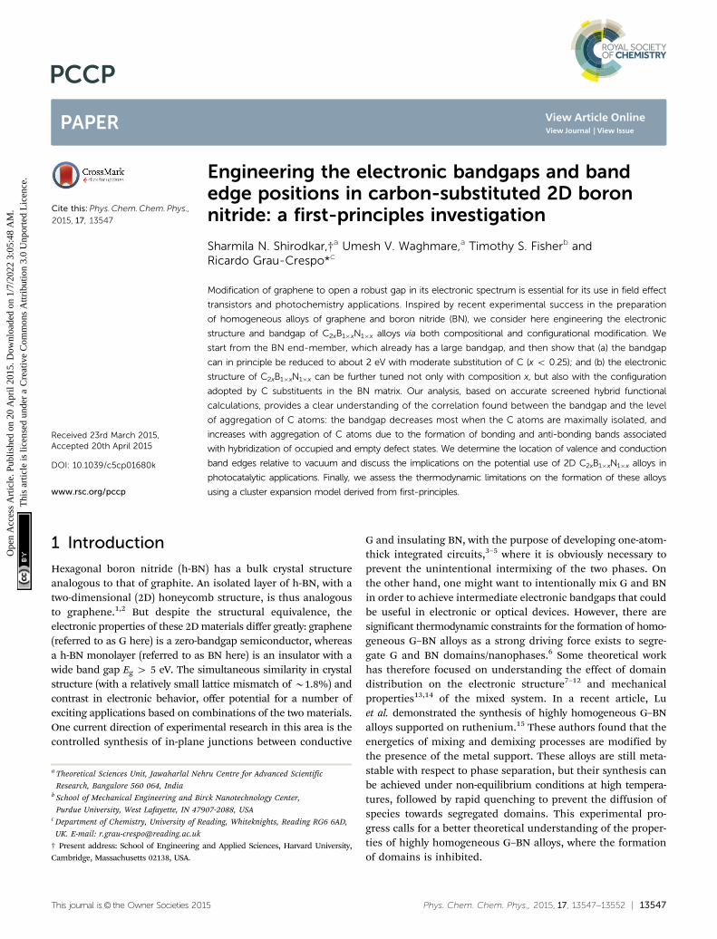
The supercell with composition C2B8N8 (x = 0.11) has only 3symmetrically different site-occupancy configurations: oneconfiguration where the two C atoms are in nearest-neighborsites, forming a C–C bond or ‘dimer’, and two configurationswithout C–C bonds. The supercell with composition C4B7N7 (x =0.22) has 30 different configurations, with varying degrees of Caggregation, ranging from the cases where all four C atoms form acluster (tetramer), to cases where each C atom is ‘‘isolated’’ (noC–C bonds). Our first observation is that configurations withhigher C content tend to have narrower bandgaps, as expectedfrom the electronic structures of pure G and BN. However, thereare also significant variations in bandgaps amongst configura-tions corresponding to the same compositions. We have plottedthe bandgap versus the average size of C clusters in each configu-ration (refer to Fig. 1). Clearly, structures with higher carbonaggregation tend to have wider band gaps as compared to thosewith smaller cluster sizes or isolated C atoms. In the C4B7N7
configuration with the narrowest bandgap (E2 eV) all the fourC atoms are isolated.
We note that a range of bandgap values still exist for a givenaverage cluster size, but this dispersion can also be explainedby the C distribution. For example, in the C4B7N7 (x = 0.22)composition, when the average cluster size is 2, there are twopossible types of configurations according to the cluster sizedistribution: configurations have either one triplet and one
Fig. 1 Variation of bandgaps with average cluster sizes in the C2B8N8 cellcomposition (x = 0.11; black circles), and in the C4B7N7 cell composition(x = 0.22; red squares). The bandgap decreases with C concentration andincreases with the average cluster size in the configuration. The bandgapof h-BN (x = 0; green diamond) is given for reference.
Paper PCCP
Ope
n A
cces
s A
rtic
le. P
ublis
hed
on 2
0 A
pril
2015
. Dow
nloa
ded
on 1
/7/2
022
3:05
:48
AM
. T
his
artic
le is
lice
nsed
und
er a
Cre
ativ
e C
omm
ons
Attr
ibut
ion
3.0
Unp
orte
d L
icen
ce.
View Article Online
This journal is© the Owner Societies 2015 Phys. Chem. Chem. Phys., 2015, 17, 13547--13552 | 13549
isolated carbon (‘‘1+3’’), or two dimers of carbon atoms (‘‘2+2’’).We find that the 1+3 configurations give bandgaps smaller thanthose of the 2+2 configurations.
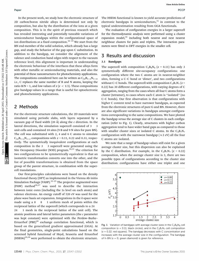
In order to understand the origin of the trend describedabove, we have studied the contribution of the orbitals fromdifferent atomic species to the electronic density of states fortwo C2B8N8 (x = 0.11) configurations: one where the C atoms areisolated, and one where they are forming a C–C dimer (seeFig. 2). We have aligned the electron energies in both cases withrespect to the vacuum level, which was determined from theelectron potential in the middle of the vacuum gap in theperiodic simulation cell. The double substitution (C at N and Cat B) gives rise to two defect states, one above the valence bandmaximum of pure BN and and one below the conduction bandminimum of pure BN, in agreement with a previous report.8
When the C substituents are separate from each other(Fig. 2(a)), the electron density corresponding to the highestoccupied band in the substituted system is clearly localized atthe C atom occupying the N site (Fig. 2(b)), whereas the densitycorresponding to the first empty band is localized at the C atom
occupying the B site (Fig. 2(c)). However, when the two C atomsform a bond, the defect states (Fig. 2(d)) arise from the mixingof the orbitals from the two C atoms. The highest occupiedstate in this case is the ‘‘bonding’’ combination (Fig. 2(e)), andthe lowest empty state is the ‘‘anti-bonding’’ combination(Fig. 2(f)). Because the energy difference between the ‘‘bonding’’and ‘‘antibonding’’ states is larger than that between the isolatedC/N and C/B defect states, the bandgap increases when dimeriza-tion occurs (as shown schematically in Fig. 2(g)). The formation ofa bonding defect state also explains why the dimerized configu-ration is strongly stabilized with respect to the configurationswith only C monomers: the calculated energy difference is 1.66 eV.We will return to the discussion of stabilities below.
3.2 Band alignment
The alignment of the band structure with reference to thevacuum level is important as a basis to understand the electro-nic behavior of interfaces involving these 2D materials. Suchreferencing also allows us to explore the potential activity inphotocatalytic applications, for example, for hydrogen productionvia water splitting. The possibility of making these nanostructuresactive for photocatalytic hydrogen production is very attractivebecause, if achieved, it could lead to simultaneous hydrogenproduction and storage in combined C/BN systems.
Assuming a single-semiconductor cell configuration, andthat other materials properties are satisfied, an ideal photo-catalyst for water splitting would have certain important char-acteristics in its electronic structure. On the one hand, thepositions of the conduction and valence band edges shouldstraddle the redox potentials for water photolysis.33–35 Thismeans that the conduction band edge should be above the energycorresponding to the hydrogen evolution reaction (HER), and thevalence band edge should be below the energy of the oxygenevolution reaction (OER), implying also that the bandgap mustbe wider than 1.23 eV (difference between the HER and theOER). In fact, once loss mechanisms are accounted for, a bandgapof 2 eV or more is generally necessary.34 On the other hand, thebandgap should not be too wide, in order to allow the adsorptionof photons from the visible part of solar radiation. It is knownthat, in the vacuum scale and at pH = 0, the HER level is locatedat �4.44 eV, and the OER level is located at �5.67 eV.36 Attemperature T and pH 4 0, these energy levels are shifted up by(kBT ln 10) � pH, where kB is Boltzmann’s constant. By referen-cing the electronic levels in our semiconductor solid solutionsto the vacuum level (taken here as the electron potential at themiddle of the vacuum gap), we can assess whether the band edgesof the semiconductor are in a favorable position to catalyze thesolar splitting of water under a given set of conditions.
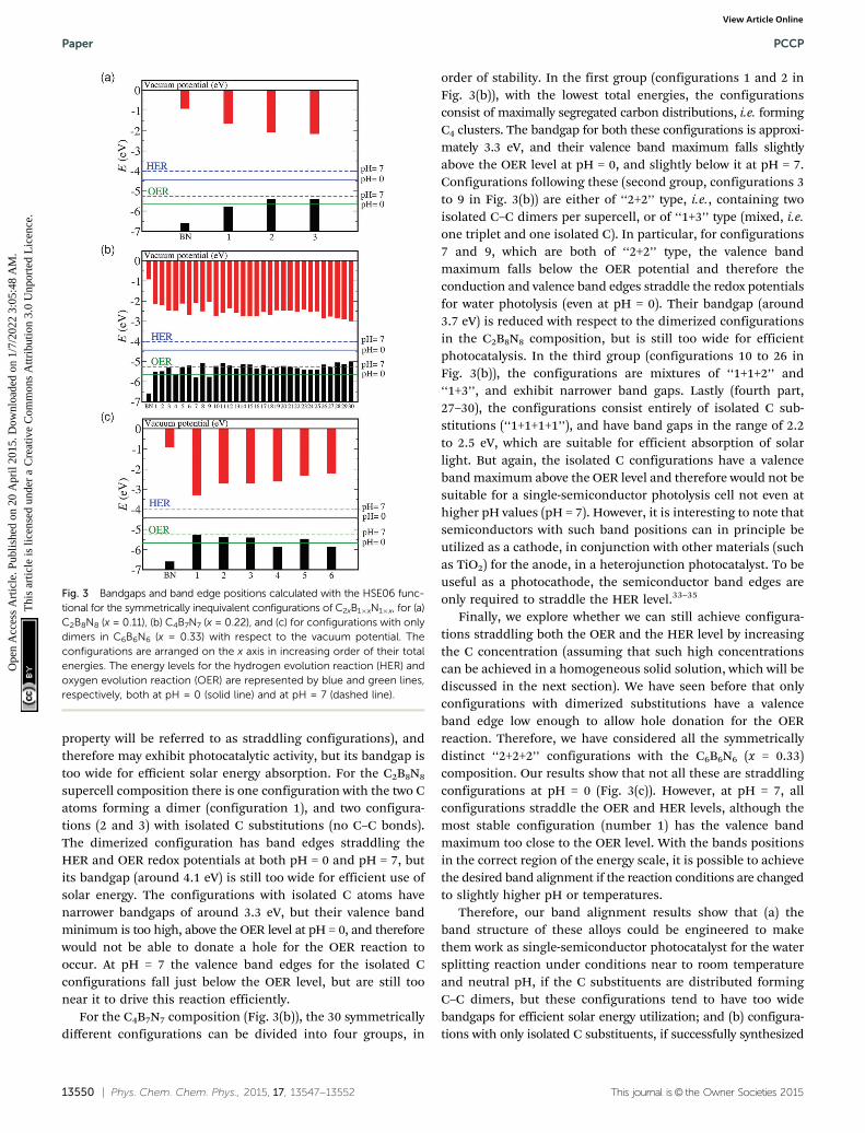
The positions of the band edges of C2B8N8 (x = 0.11) andC4B7N0.7 (x = 0.22) configurations with respect to the vacuumpotential and to the HER and OER electrode potentials at pH =0 and pH = 7 are shown in Fig. 3(a) and (b) respectively.Configurations are sorted in each case by their total energies(from lower to higher), and the band edge positions of pure BNare given for reference. Pure BN has has band edges straddlingthe HER and OER redox potentials (configurations with this
Fig. 2 Electronic density of states and charge density plot of HighestOccupied Molecular Orbital (HOMO) and Lowest Unoccupied MolecularOrbital (LUMO) for configurations with isolated (‘‘1+1’’) C atoms and dimers(‘‘2’’) in C2B8N8 (x = 0.22). (a) Density of states, and charge density plots of(b) HOMO and (c) LUMO states of ‘‘1+1’’ configuration. (d) Density of states,and charge density plots of (e) HOMO and (f) LUMO states of ‘‘2’’configuration. (g) Schematic of the formation of bonding and antibondingstates from the C/B and C/N defect states in ‘‘1+1’’ configuration. EF
denotes the Fermi energy and the dotted line at 0 is the vacuum level.Here, C = yellow, B = green and N = blue.
PCCP Paper
Ope
n A
cces
s A
rtic
le. P
ublis
hed
on 2
0 A
pril
2015
. Dow
nloa
ded
on 1
/7/2
022
3:05
:48
AM
. T
his
artic
le is
lice
nsed
und
er a
Cre
ativ
e C
omm
ons
Attr
ibut
ion
3.0
Unp
orte
d L
icen
ce.
View Article Online
13550 | Phys. Chem. Chem. Phys., 2015, 17, 13547--13552 This journal is© the Owner Societies 2015
property will be referred to as straddling configurations), andtherefore may exhibit photocatalytic activity, but its bandgap istoo wide for efficient solar energy absorption. For the C2B8N8
supercell composition there is one configuration with the two Catoms forming a dimer (configuration 1), and two configura-tions (2 and 3) with isolated C substitutions (no C–C bonds).The dimerized configuration has band edges straddling theHER and OER redox potentials at both pH = 0 and pH = 7, butits bandgap (around 4.1 eV) is still too wide for efficient use ofsolar energy. The configurations with isolated C atoms havenarrower bandgaps of around 3.3 eV, but their valence bandminimum is too high, above the OER level at pH = 0, and thereforewould not be able to donate a hole for the OER reaction tooccur. At pH = 7 the valence band edges for the isolated Cconfigurations fall just below the OER level, but are still toonear it to drive this reaction efficiently.
For the C4B7N7 composition (Fig. 3(b)), the 30 symmetricallydifferent configurations can be divided into four groups, in
order of stability. In the first group (configurations 1 and 2 inFig. 3(b)), with the lowest total energies, the configurationsconsist of maximally segregated carbon distributions, i.e. formingC4 clusters. The bandgap for both these configurations is approxi-mately 3.3 eV, and their valence band maximum falls slightlyabove the OER level at pH = 0, and slightly below it at pH = 7.Configurations following these (second group, configurations 3to 9 in Fig. 3(b)) are either of ‘‘2+2’’ type, i.e., containing twoisolated C–C dimers per supercell, or of ‘‘1+3’’ type (mixed, i.e.one triplet and one isolated C). In particular, for configurations7 and 9, which are both of ‘‘2+2’’ type, the valence bandmaximum falls below the OER potential and therefore theconduction and valence band edges straddle the redox potentialsfor water photolysis (even at pH = 0). Their bandgap (around3.7 eV) is reduced with respect to the dimerized configurationsin the C2B8N8 composition, but is still too wide for efficientphotocatalysis. In the third group (configurations 10 to 26 inFig. 3(b)), the configurations are mixtures of ‘‘1+1+2’’ and‘‘1+3’’, and exhibit narrower band gaps. Lastly (fourth part,27–30), the configurations consist entirely of isolated C sub-stitutions (‘‘1+1+1+1’’), and have band gaps in the range of 2.2to 2.5 eV, which are suitable for efficient absorption of solarlight. But again, the isolated C configurations have a valenceband maximum above the OER level and therefore would not besuitable for a single-semiconductor photolysis cell not even athigher pH values (pH = 7). However, it is interesting to note thatsemiconductors with such band positions can in principle beutilized as a cathode, in conjunction with other materials (suchas TiO2) for the anode, in a heterojunction photocatalyst. To beuseful as a photocathode, the semiconductor band edges areonly required to straddle the HER level.33–35
Finally, we explore whether we can still achieve configura-tions straddling both the OER and the HER level by increasingthe C concentration (assuming that such high concentrationscan be achieved in a homogeneous solid solution, which will bediscussed in the next section). We have seen before that onlyconfigurations with dimerized substitutions have a valenceband edge low enough to allow hole donation for the OERreaction. Therefore, we have considered all the symmetricallydistinct ‘‘2+2+2’’ configurations with the C6B6N6 (x = 0.33)composition. Our results show that not all these are straddlingconfigurations at pH = 0 (Fig. 3(c)). However, at pH = 7, allconfigurations straddle the OER and HER levels, although themost stable configuration (number 1) has the valence bandmaximum too close to the OER level. With the bands positionsin the correct region of the energy scale, it is possible to achievethe desired band alignment if the reaction conditions are changedto slightly higher pH or temperatures.
Therefore, our band alignment results show that (a) theband structure of these alloys could be engineered to makethem work as single-semiconductor photocatalyst for the watersplitting reaction under conditions near to room temperatureand neutral pH, if the C substituents are distributed formingC–C dimers, but these configurations tend to have too widebandgaps for efficient solar energy utilization; and (b) configura-tions with only isolated C substituents, if successfully synthesized
Fig. 3 Bandgaps and band edge positions calculated with the HSE06 func-tional for the symmetrically inequivalent configurations of C2xB1�xN1�x, for (a)C2B8N8 (x = 0.11), (b) C4B7N7 (x = 0.22), and (c) for configurations with onlydimers in C6B6N6 (x = 0.33) with respect to the vacuum potential. Theconfigurations are arranged on the x axis in increasing order of their totalenergies. The energy levels for the hydrogen evolution reaction (HER) andoxygen evolution reaction (OER) are represented by blue and green lines,respectively, both at pH = 0 (solid line) and at pH = 7 (dashed line).
Paper PCCP
Ope
n A
cces
s A
rtic
le. P
ublis
hed
on 2
0 A
pril
2015
. Dow
nloa
ded
on 1
/7/2
022
3:05
:48
AM
. T
his
artic
le is
lice
nsed
und
er a
Cre
ativ
e C
omm
ons
Attr
ibut
ion
3.0
Unp
orte
d L
icen
ce.
View Article Online
This journal is© the Owner Societies 2015 Phys. Chem. Chem. Phys., 2015, 17, 13547--13552 | 13551
at a reasonably high C concentration, could achieve narrowerbandgaps in the desired range for solar light absortpion butwith a valence band edge too high for single-semiconductorwater splitting photocatalysts. These configurations wouldsatisfy the band edge position requirements for a cathode ina heterojunction photocatalyst.
3.3 Stability
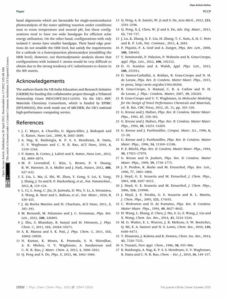
We briefly discuss here the relative energies of the configurations,and also the stability of the alloy with respect to phase separation.The calculated mixing energies (energies of the alloy with respectto the corresponding amounts of pure BN and graphene) arepositive and high for all the compositions and configurations,confirming that the alloy formation is always a highly endother-mic process (Fig. 4). For reference, we have also plotted theaverage energy of the alloy as a function of composition (seenas red line in Fig. 4), as calculated in a larger (6 � 6) cell foreach composition. This was done using a cluster expansion32
model with parameters fitted to DFT energies in the smallercell; the agreement between the energies calculated at DFT leveland those obtained from the cluster expansion is illustrated inthe inset of Fig. 4. The configurations evaluated with the clusterexpansion and included in the average energy all have theC2xB1�xN1�x stoichiometry.
The very high mixing energies shown in Fig. 4 indicate thatthe free energy of mixing, despite the stabilizing effect ofthe configurational entropy, will also be positive at any sig-nificant C concentration. To illustrate this, consider the max-imum configurational entropy for this type of alloy, using theideal expresssion:
S = �2kB(x ln x + (1�x)ln(1�x)). (1)
where the factor of 2 comes from the two sublattices with mixedoccupancy. At x = 0.1 and T = 1000 K, �ST = �56 meV performula unit, which is more than 5 times smaller in absolutevalue than the mixing energy at that composition.
We explained above how the formation of C–C bonds lowersthe total energy with respect to two isolated C atoms; we seehere that the same trend is observed for larger clusters, whichare always energetically favoured over smaller ones. Thermo-dynamics clearly drives the system towards the segregation ofBN and C domains, and against the formation of an alloy, ashas been discussed previously by other authors.6,9,15 Our resultsshow that isolated carbon substitutions are always the least stable,and are above the average energy line, particularly for higherconcentrations, which suggest that such configurations mightbe difficult to achieve. It is important to note that these alloysmust always be synthetized by a non-equilibrium procedure15,37
and therefore it is difficult to predict the extent to which theenergy differences between configurations are relevant. However,our results suggest that in a metastable sample with significant Csubstitution, obtained by quenching from high temperature,isolated C atoms would occur rarely, if at all. A sample with onlyisolated C substitutions could only be obtained by such meth-ods at very low C concentrations, where the configurationalentropy dominates the distribution. At higher C concentration,a more sophisticated synthesis technique allowing atom-by-atom control would be required. On the other hand, configura-tions with isolated C–C dimers, which are also potentiallyinteresting in photocatalysis, might be easier to synthesizebecause the C–C interaction stabilizes them with respect toisolated C substitutions. However, they are still metastable withrespect to phase segregation.
4 Conclusions
Our work elucidates the relationship between the distributionof C substituents in 2D boron nitride and the resulting electro-nic structure. We show that the bandgap decreases withincreasing C concentration, as expected, and that the reductionin gap is more pronounced the more disperse the distributionof the substituents is. Hence the smallest bandgaps for a givencomposition correspond to configurations with only isolated Csubstituents, that is, with no C–C bonds. For example, we havefound that the substitution of isolated C atoms at a concen-tration of only x = 0.22 brings the bandgap down to 2 eV.
From the point of view of potential applications in electronics,it is important to note that this small gap arises from narrowbands associated with defect states, leading to large effectivemasses and low mobilities. However, for larger concentrationsof C substitutions the edge bands become wider. Thereforewhen engineering the bandgap of this system one would needto find a balance between gap opening and mobility.
The analysis of the electronic structure shows that theclustering of the C substituents leads to mixing of the wave-functions corresponding to these defect states, forming bond-ing and anti-bonding levels. This effect is responsible for theincrease in the band gap with C clustering.
We have also reported the variation of the band edgepositions with respect to composition and ion distribution.We found that configurations consisting of C–C dimers have
Fig. 4 Crosses show the DFT mixing energies (per formula unit) forC2xB1�xN1�x configurations and the red line represents the average mixingenergies calculated for a converged sample of random configurationsusing a cluster expansion model. Inset shows the mixing energies pre-dicted by the model versus DFT for C2xB1�xN1�x.
PCCP Paper
Ope
n A
cces
s A
rtic
le. P
ublis
hed
on 2
0 A
pril
2015
. Dow
nloa
ded
on 1
/7/2
022
3:05
:48
AM
. T
his
artic
le is
lice
nsed
und
er a
Cre
ativ
e C
omm
ons
Attr
ibut
ion
3.0
Unp
orte
d L
icen
ce.
View Article Online
13552 | Phys. Chem. Chem. Phys., 2015, 17, 13547--13552 This journal is© the Owner Societies 2015
band alignments which are favourable for single-semiconductorphotocatalysis of the water splitting reaction under conditionsnear to room temperature and neutral pH, but these config-urations tend to have too wide bandgaps for efficient solarenergy utilization. On the other hand, configurations with onlyisolated C atoms have smaller bandgaps. Their band edge posi-tions do not straddle the OER level, but satisfy the requirementsfor a cathode in a heterojunction photocatalyst (straddling theHER level). However, our thermodynamic analysis shows thatconfigurations with isolated C atoms would be very difficult toobtain due to the strong tendency of C substituents to cluster inthe BN matrix.
Acknowledgements
The authors thank the UK-India Education and Research Initiative(UKIERI) for funding this collaborative project through a TrilateralPartnership Grant IND/CONT/2013-14/054. Via the UK’s HPCMaterials Chemistry Consortium, which is funded by EPSRC(EP/L000202), this work made use of ARCHER, the UK’s nationalhigh-performance computing service.
References
1 J. C. Meyer, A. Chuvilin, G. Algara-Siller, J. Biskupek andU. Kaiser, Nano Lett., 2009, 9, 2683–2689.
2 A. Nag, K. Raidongia, K. P. S. S. Hembram, R. Datta,U. V. Waghmare and C. N. R. Rao, ACS Nano, 2010, 4,1539–1544.
3 P. Sutter, R. Cortes, J. Lahiri and E. Sutter, Nano Lett., 2012,12, 4869–4874.
4 M. P. Levendorf, C. Kim, L. Brown, P. Y. Huang,R. W. Havener, D. A. Muller and J. Park, Nature, 2012, 488,627–632.
5 Z. Liu, L. Ma, G. Shi, W. Zhou, Y. Gong, S. Lei, X. Yang,J. Zhang, J. Yu and K. P. Hackenberg, et al., Nat. Nanotechnol.,2013, 8, 119–124.
6 L. Ci, L. Song, C. Jin, D. Jariwala, D. Wu, Y. Li, A. Srivastava,Z. Wang, K. Storr and L. Balicas, et al., Nat. Mater., 2010, 9,430–435.
7 J. da Rocha Martins and H. Chacham, ACS Nano, 2011, 5,385–393.
8 M. Bernardi, M. Palummo and J. C. Grossman, Phys. Rev.Lett., 2012, 108, 226805.
9 J. Zhu, S. Bhandary, B. Sanyal and H. Ottosson, J. Phys.Chem. C, 2011, 115, 10264–10271.
10 A. K. Manna and S. K. Pati, J. Phys. Chem. C, 2011, 115,10842–10850.
11 N. Kumar, K. Moses, K. Pramoda, S. N. Shirodkar,A. K. Mishra, U. V. Waghmare, A. Sundaresan andC. N. R. Rao, J. Mater. Chem. A, 2013, 1, 5806–5821.
12 Q. Peng and S. De, Phys. E, 2012, 44, 1662–1666.
13 Q. Peng, A. R. Zamiri, W. Ji and S. De, Acta Mech., 2012, 223,2591–2596.
14 Q. Peng, X.-J. Chen, W. Ji and S. De, Adv. Eng. Mater., 2013,15, 718–727.
15 J. Lu, K. Zhang, X. F. Liu, H. Zhang, T. C. Sum, A. H. C. Netoand K. P. Loh, Nat. Commun., 2013, 4, 2681.
16 P. Piquini, P. A. Graf and A. Zunger, Phys. Rev. Lett., 2008,100, 186403.
17 Y. Seminovski, P. Palacios, P. Wahnon and R. Grau-Crespo,Appl. Phys. Lett., 2012, 100, 102112.
18 D. O. Scanlon and A. Walsh, Appl. Phys. Lett., 2012,100, 251911.
19 D. Santos-Carballal, A. Roldan, R. Grau-Crespo and N. H.de Leeuw, Phys. Rev. B: Condens. Matter Mater. Phys., 2015,in press, http://arxiv.org/abs/1504.00268.
20 R. Grau-Crespo, S. Hamad, C. R. A. Catlow and N. H.de Leeuw, J. Phys.: Condens. Matter, 2007, 19, 256201.
21 R. Grau-Crespo and U. V. Waghmare, in Molecular Modelingfor the Design of Novel Performance Chemicals and Materials,ed. B. Rai, CRC Press, 2012, ch. 11, pp. 303–326.
22 G. Kresse and J. Hafner, Phys. Rev. B: Condens. Matter Mater.Phys., 1993, 47, 558–561.
23 G. Kresse and J. Hafner, Phys. Rev. B: Condens. Matter Mater.Phys., 1994, 49, 14251–14269.
24 G. Kresse and J. Furthmuller, Comput. Mater. Sci., 1996, 6,15–50.
25 G. Kresse and J. Furthmuller, Phys. Rev. B: Condens. MatterMater. Phys., 1996, 54, 11169–11186.
26 P. E. Blochl, Phys. Rev. B: Condens. Matter Mater. Phys., 1994,50, 17953–17979.
27 G. Kresse and D. Joubert, Phys. Rev. B: Condens. MatterMater. Phys., 1999, 59, 1758–1775.
28 J. P. Perdew, K. Burke and M. Ernzerhof, Phys. Rev. Lett.,1996, 77, 3865–3868.
29 J. Heyd, G. E. Scuseria and M. Ernzerhof, J. Chem. Phys.,2003, 118, 8207–8215.
30 J. Heyd, G. E. Scuseria and M. Ernzerhof, J. Chem. Phys.,2006, 124, 219906.
31 J. Heyd, J. E. Peralta, G. E. Scuseria and R. L. Martin,J. Chem. Phys., 2005, 123, 174101.
32 C. Wolverton and D. de Fontaine, Phys. Rev. B: Condens.Matter Mater. Phys., 1994, 49, 8627–8642.
33 H. Wang, L. Zhang, Z. Chen, J. Hu, S. Li, Z. Wang, J. Liu andX. Wang, Chem. Soc. Rev., 2014, 43, 5234–5244.
34 M. G. Walter, E. L. Warren, J. R. McKone, S. W. Boettcher,Q. Mi, E. A. Santori and N. S. Lewis, Chem. Rev., 2010, 110,6446–6473.
35 T. Hisatomi, J. Kubota and K. Domen, Chem. Soc. Rev., 2014,43, 7520–7535.
36 S. Trasatti, Pure Appl. Chem., 1986, 58, 955–966.37 K. Raidongia, A. Nag, K. P. S. S. Hembram, U. V. Waghmare,
R. Datta and C. N. R. Rao, Chem. – Eur. J., 2010, 16, 149–157.
Paper PCCP
Ope
n A
cces
s A
rtic
le. P
ublis
hed
on 2
0 A
pril
2015
. Dow
nloa
ded
on 1
/7/2
022
3:05
:48
AM
. T
his
artic
le is
lice
nsed
und
er a
Cre
ativ
e C
omm
ons
Attr
ibut
ion
3.0
Unp
orte
d L
icen
ce.
View Article Online

![Cutting Edge Upper Intermediate 3rd Edition Wordlist...Cutting Edge Upper Intermediate 3rd Edition Wordlist studio 8 n [C] /ˈstjuːdiəʊ , ˈstuːdioʊ/ Studio The band spent just](https://img.pdfslide.us/doc/110x75/5f1eacbbe1ce9474b21f850c/cutting-edge-upper-intermediate-3rd-edition-wordlist-cutting-edge-upper-intermediate.jpg)