Embed Size (px)
Citation preview

Engineer-to-Engineer Note EE-209
a
Technical notes on using Analog Devices DSPs, processors and development toolsVisit our Web resources http://www.analog.com/ee-notes and http://www.analog.com/processors ore-mail [email protected] or [email protected] for technical support.
Asynchronous Host Interface on ADSP-21161N SHARC® Processors Contributed by R.Hoffmann Rev 2 – September 5, 2007
Copyright 2003-2007, Analog Devices, Inc. All rights reserved. Analog Devices assumes no responsibility for customer product design or the use or application of customers’ products or for any infringements of patents or rights of others which may result from Analog Devices assistance. All trademarks and logos are property of their respective holders. Information furnished by Analog Devices applications and development tools engineers is believed to be accurate and reliable, however no responsibility is assumed by Analog Devices regarding technical accuracy and topicality of the content provided in Analog Devices Engineer-to-Engineer Notes.
Introduction This EE-note explains the functional operation and usage of the ADSP-21161N SHARC® processor asynchronous host interface for uni-processor- and multi-processor systems. Furthermore, booting is covered including its host loader kernel. The system is based on the ADSP-21161N SHARC processor acting as slave and the ADSP-21065L SHARC processor emulating a host microprocessor and acting as the system’s master. Note that this EE-Note may also be used as a reference for other SHARC members featuring a host interface.
Family Overview
The host interface is present in the following SHARC family members:
Processor ADSP-2106x/M ADSP-21065L ADSP-21160M/N ADSP-21161N
Host bus width 16, 32 8, 16, 32 16, 32 8, 16, 32
DMA data
packing
16:32, 16:48, 32:48 8:32, 16:32, 8:48,
16:48, 32:48
16:32/64, 32:32/64,
16:48, 32:48
8:32/64,16:32/64, 32:32/64,
8:48, 16:48, 32:48
Access Timing synchr / asynchr asynchr synchr / asynchr asynchr
Host Speed 50 MHz 33 MHz 50 MHz 50 MHz
Internal Access IOP/Block0/1 IOP IOP/Block0/1 IOP
Host Booting Yes Yes Yes Yes
Table 1: Host interface feature overview

a
Asynchronous Host Interface on ADSP-21161N SHARC® Processors (EE-209) Page 2 of 40
Content Introduction .................................................................................................................................................................................................1
Family Overview .....................................................................................................................................................................................1 Content .............................................................................................................................................................................................................2 Host Interface.............................................................................................................................................................................................4
Pin Description and Pin States during and after Reset ...........................................................................................4 Speed.............................................................................................................................................................................................................5 IOP Registers..........................................................................................................................................................................................5 Direct and Indirect Data Transfers ........................................................................................................................................5 Data Path and Packing .......................................................................................................................................................................6 Timing Requirements............................................................................................................................................................................7
Case 1:...................................................................................................................................................................................................8 Case 2:...................................................................................................................................................................................................8
Uni-processor System ............................................................................................................................................................................10 Pull-up Resistances..........................................................................................................................................................................11 Unbuffered Signals ............................................................................................................................................................................11 Buffered Signals.................................................................................................................................................................................11 Host Access to DSP ............................................................................................................................................................................12 Host Access to SRAM and SBSRAM................................................................................................................................................13 Host Access to SDRAM .......................................................................................................................................................................14 Continuous Host Access ..................................................................................................................................................................15
Multi-processor System........................................................................................................................................................................15 Pull-up Resistances..........................................................................................................................................................................16 Unbuffered Signals ............................................................................................................................................................................16 REDY for Multi-processing ...........................................................................................................................................................16 Buffered Signals.................................................................................................................................................................................17 Host Broadcast Writes .....................................................................................................................................................................17
Uni-Processor Booting ..........................................................................................................................................................................18 Elfloader Utility ..............................................................................................................................................................................18 Loader Output File ............................................................................................................................................................................19 Hardwired Boot DMA ............................................................................................................................................................................21
DMA: ........................................................................................................................................................................................................21 CORE: .....................................................................................................................................................................................................21
Host Loader Kernel ............................................................................................................................................................................21 Functionality of 161_host.dxe ..................................................................................................................................................22
Step 1 ...................................................................................................................................................................................................24 Step 2 ...................................................................................................................................................................................................24 Step 3:.................................................................................................................................................................................................25

a
Asynchronous Host Interface on ADSP-21161N SHARC® Processors (EE-209) Page 3 of 40
Step 4:.................................................................................................................................................................................................26 Step 5:.................................................................................................................................................................................................26 Step 6:.................................................................................................................................................................................................26 Step 7:.................................................................................................................................................................................................27 Step 8:.................................................................................................................................................................................................27 Step 9:.................................................................................................................................................................................................27 Step 10: ..............................................................................................................................................................................................28
Timing for 161_host.dxe ................................................................................................................................................................28 Host Timeout ..........................................................................................................................................................................................29 64-bit Boot Sections .......................................................................................................................................................................32 General Steps for Booting ...........................................................................................................................................................32 Loader Kernel Customization.......................................................................................................................................................32
Example 1:..........................................................................................................................................................................................32 Example 2:..........................................................................................................................................................................................32
Boot Timing DSP with External Memory .................................................................................................................................33 Booting C/C++ Programs ..................................................................................................................................................................34
Multi-processor Booting .....................................................................................................................................................................35 Elfloader Utility ..............................................................................................................................................................................35 Shared Memory........................................................................................................................................................................................37 Boot Timing Cluster DSP with Shared Memory ...................................................................................................................37
Debug Issues ...............................................................................................................................................................................................38 Modification of LDR-file..............................................................................................................................................................38 Booting without Loader Kernel ..................................................................................................................................................38 Steps for Diagnostic .......................................................................................................................................................................39 Emulation Issues.................................................................................................................................................................................39
DMA activities ................................................................................................................................................................................39 Core activities..............................................................................................................................................................................40 Entire boot scenario ..................................................................................................................................................................40
References ....................................................................................................................................................................................................40 Document History ......................................................................................................................................................................................40

a
Asynchronous Host Interface on ADSP-21161N SHARC® Processors (EE-209) Page 4 of 40
Host Interface The host interface enables easy connection to standard 8-bit, 16-bit or 32-bit microprocessor buses with little additional hardware required. The ADSP-21161N SHARC processor accommodates asynchronous data transfers, allowing the host to use a different clock frequency. Asynchronous transfers at speeds up to 50 MHz, the host interface is accessed through the ADSP-21161N external port (Figure 1). The host interface is memory-mapped into the unified address space of the ADSP-21161N processor.
Figure 1. Internal Memory (dual-ported SRAM), DMA-controller (I/O Processor) and host port (External port)
Pin Description and Pin States during and after Reset
This section describes which pins have to be used for the host interface [1]. Table 1 illustrates all relevant host signals used to design a host interface. The state during and after reset is important, based on that, some signals require buffers or not. Buffered and un-buffered signals are covered in more detail later on.
Pin Type Description State during and after reset
~CS I Chip Select Input
~HBR I/A Host Bus Request Input
~SBTS I/S Suspend Bus and Three-state Input
~HBG I/O/S/T Host Bus Grant Driven high (ID=0 or 1)
REDY(o/d) O Host Bus Acknowledge Three state
ACK I/O/S MMS ext. Memory Acknowledge Tied high with internal pull-up
~RD I/O/T Memory Read strobe Driven high (ID=0 or 1)
~WR I/O/T Memory Write strobe Driven high (ID=0 or 1)

a
Asynchronous Host Interface on ADSP-21161N SHARC® Processors (EE-209) Page 5 of 40
A[23:0] I/O/T External Bus Address Driven high (ID=0 or 1)
D[47:16] I/O/T External Bus Data Three state I=input, O=output, S=synchronous, T=three state, A=asynchronous
Table 2: Host interface pin description
Speed
The External Port speed of the host interface is depending on the CLKIN/XTAL configuration and the setting of the clock doubling pin (~CLKDBL). The maximum clock is 50 MHz and can be obtained with the CLKOUT pin [1].
IOP Registers
IOP registers are used by the host for communication with the processor. It this is the only way for the host to access the processor internal resources. Next table lists the most important used [2].
Register IOP-Address Comment
SYSCON 0x0 System control
VIRPT 0x1 Vector interrupt
WAIT 0x2 Wait mode and Wait states
SYSTAT 0x3 System status
EPB0 0x4 External Port Buffer 0
MSGR0-7 0x7-0xF Message registers
DMAC10 0x1C DMA channel 10 control
SDCTL 0xB8 SDRAM control
SDRDIV 0xB9 SDRAM refresh
Table 3: Most important IOP registers
The DSP uses following prioritization scheme for IOP-register accesses:
1. EP-bus (Host)
2. DM-bus (slave core)
3. PM-bus (slave core)
4. IO-bus (slave DMA activity)
The bus with highest priority gets access to the registers and the other buses are held off until that access has been completed.
Direct and Indirect Data Transfers
In order for the host to be able to directly access memory blocks 0/1 over the external port, direct write FIFOs would be needed. However, these FIFOs have not been implemented in the ADSP-21161N SHARC processor.

a
Asynchronous Host Interface on ADSP-21161N SHARC® Processors (EE-209) Page 6 of 40
Figure 2: The memory blocks 0 and 1 can be accessed with a DMA, called indirect access. For this reason, a host processor can only directly access the IOP-registers over the external port. This is known as a direct access. Additionally, the host processor can also access memory blocks 0 and 1 via Direct Memory Access (DMA). This is known as an indirect access.
Figure 2. Direct Write FIFOs on ADSP-21160M/N processors
Data Path and Packing
Because the 8-, 16- and 32-bit transfers are supported, a packing unit becomes active. Two IOP registers are responsible for the host packing scenario:
Register Bits Comment Settings
SYSCON HBW Host bus width 8, 16, 32 bits
SYSTAT HPS Host packing status pack complete until 5th stage of packing
DMACx PMODE DMA data packing 8:32/64, 8:48, 16:32/64, 16:48, 32:32/64, 32:48 bits
Table 4: Packing mode overview
Host bus width (HBW-bits/SYSCON), responsible for the external bus width, will gate all ongoing read or writes to 8,16 or 32-bits. Destination accesses to Parameter, Control or Status IOP-registers are using fixed internal packing to 32-bit. The DMA packing (PMODE-bits/DMACx) is ignored during this access. If packing selected (8,16 bits), the host must write to all 32-bits in packed mode.
For host DMAs, the situation is different: The destination width can vary from 32, 48 to 64-bits, based on (PMODE-bits/DMACx) and the host bus width (HBW-bits/SYSCON). For host booting, the destination width is 48 bits (8:48, 16:48 and 32:48) [2].

a
Asynchronous Host Interface on ADSP-21161N SHARC® Processors (EE-209) Page 7 of 40
Important: there is only one packing unit available, host must complete each packed transfer before another is begun. If not, data are not transferred to that IOP-register. The status can be read during packing (HPS-bits/SYSTAT).
Figure 3 shows the data flow to or from the slave. If an External Port Buffer (EPBx) access is done, the pack unit, depending on the packing mode (PMODE-bits/DMACx), responsible for internal bus packing, will order the data in the desired manner to write the entire word into the EPBx buffer. The DMA controller just repeats this scenario until the counter for slave DMA has expired.
EPB0FIFO
8 deep
Internalmemory
IOD 47:0
IOA 17:0
ExternalBusParameter
ControlStatus
Shadow WriteFIFO
2 deep Slave WriteFIFO
4 deep
IOProcessor
REDY
EPD 32:0
A 8:0
D 47:16
HBW-bits
Packer
HostInterface
EPA 8:0
PMODE-bits
EPD 32:0
indirect
transfers direct
transfers
On chip
EPA 8:0
SlaveControlLogic
~HBR
~CS
~HBG
ACK
Figure 3. Slave data flow with slave control logic
The slave control logic tells the host if the slave is ready:
• allow bus mastership with ~HBG
• accept data with REDY
~HBG is controlled by:
• ~HBR
• ACK
REDY is controlled by:
• ~HBR, ~CS and ~HBG signals
• EPBx FIFO, packer unit and slave write FIFO
Timing Requirements
The design of a host interface requires study of slave’s datasheet timing [1]. Some points must be taken into consideration:

a
Asynchronous Host Interface on ADSP-21161N SHARC® Processors (EE-209) Page 8 of 40
The host must assert ~HBR and ~CS for an IOP-register access (timing 1). The last cycle before assertion of ~HBG is “called bus transition cycle” (BTC). In this timeslot, the bus-master drives signals inactive before tristate. The cycle after the assertion of ~HBG is called “host transition cycle” (HTC). The host is now responsible driving following signals: A[23:0], ~MS[3:0], ~RD, ~WR, ~PA, CLKOUT, ~DMAG[1-2].
After spec tHBGRCSV, the slave starts sampling the host’s ~RD, ~WR, and ~CS. REDY is considered as a slave control signal.
Basically, there are 2 cases for REDY:
Case 1: Assertion of ~CS before HTC has occurred will immediately de-asserted REDY after spec tDRDYCS. REDY will stay low indicating that the HTC cycle is still pending until spec tTRDYHG is meet. This is useful because the assertion of any strobe will automatically be extended until the interface starts sampling the inputs.
Case 2: Assertion of ~CS after HTC meeting spec tTRDYHG will not de-assert REDY because the host already allows sampling ~RD, ~WR, and ~CS lines.
A special consideration applies to the state of REDY: by default, this pin is configured to an open drain (o/d). In uni-processor system, this open drain will be changed to active drive (a/d) by writing to ADRDY-bit/SYSCON.
It takes a minimum of 2 CLKOUT cycles from when the host processor requests the bus, until the DSP grants the bus to the host. That is from assertion of ~HBR until assertion of ~HBG assertion (1 cycle for ~HBR recognition, 1 cycle for BTC). De-assertion of ~HBR will de-assert ~HBG one CLKOUT cycle later following a BTC cycle to resume driving the bus signals. This is not valid if the current master has recognized ACK low (access pending) during BTC. In this case, ~HBG will stay de-asserted.
After ~HBG is de-asserted, the DSP restarts driving the signals after spec tMENHBG (timing 2).
Timing 1: Slave to Host Timing

a
Asynchronous Host Interface on ADSP-21161N SHARC® Processors (EE-209) Page 9 of 40
Timing 2: Host to Slave Timing
For reads (timing 3), the host must ensure proper address/chip select setup time spec tSADRDL and hold time spec tHADRDH. After latching the host address for reads, REDY is automatically de-asserted and re-asserted when data are available to drive them off-chip depending on slave’s core speed spec tRDYPRD.
For writes (timing 4), the chip select setup time spec tSCSWRL and hold time spec tHCSWRH are relevant. During writes, REDY is only de-asserted if the FIFOs are full. The next strobe access can occur if the spec tWRWH is satisfied.
Generally, if the setup/hold times are violated, the host interface may end up latching an illegal address. Therefore, the host will force a deadlock with REDY de-asserted. Do not de-assert ~RD or ~WR after an HTC while REDY de-asserted, this will also cause a core hang [2].
Timing 3: Host Read Timing

a
Asynchronous Host Interface on ADSP-21161N SHARC® Processors (EE-209) Page 10 of 40
Timing 4: Host Write Timing
Uni-processor System Figure 4 explains how to realize a host interface between host and slave. It shows the connection between the ADSP-21065L EZ-KIT Lite® and the ADSP-21161N EZ-KIT Lite evaluation boards.
Slave
ADSP-21161Nrev1.2ID=0
8-bitHost
ADSP-21065Lrev0.3ID=0
~RD
~WR
ACK
~RD
~WR
(Active drive) REDY
~HBR
~HBG
A[0:7]
D[23:16] D[0:7]
A[0:7]
74LV245
~OE DIR
VDD
FLAG0
A[8] A[8]
~BMS=1LBOOT=0EBOOT=0
Bx Ax
Slavepu 10k~SBTSREDY~HBG~HBR~CS
Hostpu 10k
~RD~WR
ACKinternal keeper
latch~RD, ~WR
internal pu 10k
VDD
FLAG3
Data
74LV245
~OE DIR
Bx Ax
74LV245~OE DIR
Bx Ax
Control
Address
~MS0~CS
Figure 4. Schematic for uni-processor system

a
Asynchronous Host Interface on ADSP-21161N SHARC® Processors (EE-209) Page 11 of 40
In order to avoid bus contention, some of the signals used for the host interface require bus transceivers [3] based on the pin state after and during reset.
Pull-up Resistances
It is recommended to use pull-up resistances of 10 kOhms for inputs (~HBR, ~CS, ~SBTS) and outputs (~HBG, REDY). The strobes use internal pull-up of 20 kOhms, valid for ID=0,1 only.
Unbuffered Signals
~HBR, ~HBG and REDY are directly connected to the host to control the requests and grants. ~HBG will be used to enable the transceivers after the BTC has occurred. The handshake between the host and slave occurs in two ways:
The 1st is realized with hardware: connection of slave control (REDY) and the host’s acknowledge (ACK). This ensures proper accesses of internal resources of the DSP. The host’s parallel port should support external acknowledge and internal wait states. Since REDY and ACK are directly tied together, there is no need of SW-polling. It is strongly recommended to use the handshake (slave control) for host accesses; its value guarantees the best performance regarding bus activities. If not used, data corruption can happen during HTC. Furthermore, any host read access and full FIFOs caused by IO-processor activities will cause problems.
If the host wants to access external memories, REDY is here not useful as it serves for internal accesses only. Therefore a second handshake mode is needed by having the host poll ~HBG signal. This can be implemented by using an IO-flag as shown in Figure 4. Polling is required because the timeslot between assertion of ~HBR and ~HBG can vary based on external accesses.
Buffered Signals
Uni-processor ID=0
Address Bits Type Comments
ADDR[0-8] IOP Must be driven
ADDR[9-16] Int. memory floating
ADDR[17:19] S-field floating
ADDR[20] M-field floating
ADDR[21-23] E-field floating
Data Bits
Data[23:16] 8-bit
Data[31:16] 16-bit
Data[47:16] 32-bit
Table 5: Required address lines for uni-processor systems
Signals, which are driven by the DSP out of reset should be buffered. This is valid for address and strobes. The host needs just to drive the IOP-addresses [0:8]. All remaining addresses can be floating. The host data width can vary between 8, 16 or 32-bits. The data are three-state after reset. If the slave uses external

a
Asynchronous Host Interface on ADSP-21161N SHARC® Processors (EE-209) Page 12 of 40
bus, it is required to buffer them as well. Furthermore, the read strobe is used to control the flow direction in the data transceiver.
The ~CS pin is derived from the host’s internal address decode logic (~MS0 pin). The assertion/de-assertion of ~MS0 is provided by the external port on ADSP-21065L processors [4]. To meet address/chip select setup/hold times, an additional buffer will delay ~CS independent from ~HBG. This is necessary for the handshake, REDY is immediately de-asserted for ~HBR and ~CS low.
Host Access to DSP
Capture 1 shows a host access during MMS activities. Assertion of ~HBR and ~CS de-asserts REDY immediately. The current bus transfer will be finished following a BTC. After the transceiver is enabled by ~HBG, ~WR is extended by REDY. After HTC is done, REDY is re-asserted to allow the host writing to message registers (MSRG0-7). The de-assertion of ~HBR will de-assert ~HBG before BTC. The slave resumes previous transfers.
Capture 1: Assertion of ~Strobes before ~HBG asserted
Capture 2: the ~WR strobe is asserted after HTC. The handshake for REDY needs not to be active, REDY will not be de-asserted indicating that the HTC is satisfied and the write can directly occur.
Capture 2: Assertion of ~Strobes after ~HBG low

a
Asynchronous Host Interface on ADSP-21161N SHARC® Processors (EE-209) Page 13 of 40
Capture 3: Slave control for 8:48-bit packing
Capture 3 demonstrates an active slave control: If the host writes “erroneously” to the disabled EPB1 FIFO (DMAC11=0x160), following happens: As the EPBx FIFOs are 8 deep, the packer unit will fill 48x8-bit words. The next 5x8-bit will fill up the packer itself. The 6th word is not accepted because of the full FIFO. Now, the slave-write FIFO comes into play. The 4-deep asynchronous FIFO stores additional 4x8-bits. Finally, all existent FIFOs are full, the slave de-asserts REDY after 48+5+4=57 writes. After this scenario, DMAC11=0xA30160 indicating FIFO buffer status full (FS-bit=3). This example demonstrates how the relevant FIFOs are working together until stalls are inserted.
Packing EPBx FIFO Packer Slave Write FIFO Sum of FIFOs
8:48 48x 8-bit 5x 8-bit 4x 8-bit 57x 8-bit
16:48 24x 16-bit 2x 8-bit 4x 16-bit 30x 16-bit
32:48 12x 32-bit 1x 8-bit 4x 32-bit 17x 32-bit
Table 6: Relevant FIFOs for host accesses
Host Access to SRAM and SBSRAM
The host may also communicate directly with system peripherals such as memories. Capture 4: With ~HBR assertion, the DSP automatically grants the bus with ~HBG low. After the host detects ~HBG low, it needs to select the external Memory with ~MS1, which is not driven during host accesses. Hereby, REDY and ~CS pins are inactive since the DSP is not accessed. The host transfer occurs using the protocol of the peripheral for SRAM, SBSRAM. If a bunch of data has to be transferred, the external handshake DMA is the right choice, which is supported for SRAM and SBSRAM. Additionally, the propagation delay of the transceiver can be recognized by the shift between signals ~Host_WR/~WR and ~Host_RD/~RD.

a
Asynchronous Host Interface on ADSP-21161N SHARC® Processors (EE-209) Page 14 of 40
Capture 4: Access to external SRAM
Figure 5. Required steps for host access to SDRAM
Host Access to SDRAM
For SDRAMs, a special situation occurs concerning bus conflict and refresh. Therefore, a direct access to SDRAM is not supported. Two SDRAM controllers, which share an SDRAM, can pass each the bus-mastership only during the self-refresh command. This requires OR logic for the CKE pins between both SDRAM controllers and the SDRAM. The remaining control signals (CLK, ~CS, ~RAS, ~CAS, ~WE and DQM are also enabled by the bus transceiver with ~HBG. The address lines must by provided from A[0:9, SDA10, 11:14] including the bank select pins.
Before the host starts asserting ~HBR, its own controller should be in self-refresh mode. After the host drives the bus, it should write to bring SDRAM into self-refresh base by de-asserting the SDCKE pin.
The SDRAM is refreshed internally and only controlled by the level of the CKE pin.
The host SDRAM controller asserts CKE to get control over the memory. Now, DMA transfers between Host and SDRAM are allowed. At the end, the host de-asserts the CKE pin by setting the self-refresh bit.
SDCKE
CKE_Host
CKE_SDRAM
~HBG
~HBR
host controlsSDRAM
ADSP-21161N controlsSDRAM
ADSP-21161N controlsSDRAM
1
2
3
4 5
6
7
SDRAMin
self-refresh
SDRAMin
self-refresh

a
Asynchronous Host Interface on ADSP-21161N SHARC® Processors (EE-209) Page 15 of 40
Now it must write to the slave’s VIRPT register which contains a dummy access to the SDRAM space. The slave now gets control back by restarting auto-refresh base. Finally, host de-asserts ~HBR.
Any of both controllers may init the device with MRS command. This requires equivalent settings like burst- length and type, CAS Latency. For the other parameters like refresh-period, row activation and precharge time, the same applies.
Following steps are required (Figure 5):
1. Host SDRAM controller in self-refresh, CKE_host => low, clock frozen
2. Host asserts ~HBR/~CS
3. Host writes to SDSRF-bit/SDCTL (self-refresh), SDCKE => low, clock frozen
4. Host releases self-refresh and access to SDRAM, CKE_Host => high, clock released
5. Host returns into self-refresh, SDCKE => low
6. Host writes to slave’s VIRPT, release self-refresh of the ADSP-21161N processors, SDCKE => high, clock released
7. Host de-asserts ~HBR/~CS
Continuous Host Access
Capture 5 illustrates what happens if the ~HBR and ~CS lines are continuously tied to ground. De-assertion of ~RESET is only allowed after the spec tCLKRST is meet. The rising edge of ~RESET starts itself a counter spec tCORERST, which expires after a maximum of 4081 CLKIN cycles. Finally, ~RSTOUT pin transitions high indicating a locked PLL. The DSP still drives the addresses and strobes during ~RSTOUT asserted. After this sequence, ~HBR is sampled and the grant is returned to allow the host transition cycle (HTC). It is not allowed to map the part to ID=2-6 as uni-processor. In this case, the slave will not return a host bus grant. If for some reasons the DSP needs the bus rarely, it can do a request by using ID=1 (instead of zero). The host should poll this pin. For any external bus transfer, ~BR1 is now asserted, but the transfer can’t be done until the host deasserts ~HBR [1].
Capture 5: ~HBR and ~CS tied to Ground
Multi-processor System Figure 6 illustrates how to build the interface between a host and multiple slaves. It shows the connection between the ADSP-21065L EZ-KIT Lite and a multi-processor board containing two ADSP-21161N SHARC processors.

a
Asynchronous Host Interface on ADSP-21161N SHARC® Processors (EE-209) Page 16 of 40
Slaves
ADSP-21161Nrev1.2ID=1ID=2
8-bitHost
ADSP-21065Lrev0.3ID=0
~RD
~WR
ACK
~RD
~WR
(Open drain) REDY
~HBR
~HBG
A[0:7]
D[23:16] D[0:7]
A[0:7]
~OE DIR
VDD
FLAG0
A[8] A[8]
~BMS=1LBOOT=0EBOOT=0
Bx Ax
Slavepu 10k~SBTS~HBG~HBR~CS1~CS2
Hostpu 10k
~RD~WR
ACKinternal keeper
latch~RD, ~WR
internal pu 10k
VDD
FLAG3
Data
74LV245
~OE DIR
Bx Ax
74LV245~OE DIR
Bx Ax
Control
Address
R=330 Ohms
VDDEXT
GNDA[20]
FLAG1~CS1
FLAG2~CS2
Figure 6. Schematic for dual multi-processor system
Pull-up Resistances
It is recommended to use pull-up resistances of 10kOhms for inputs (~HBR, ~CS, ~SBTS, ~RD, ~WR) and output (~HBG).
Unbuffered Signals
~HBR, ~HBG, REDY and ~CS1/2 are directly connected to the host to control the requests and grants. ~HBG will be used to enable the transceivers after the BTC has occurred. Using IO-flags for ~CS1/2 allows a more flexible solution for simultaneously assertion of both ~CS lines during a broadcast write in the multiprocessor system.
REDY for Multi-processing
A special consideration applies to REDY. By default, this pin is configured to an open drain, useful in a multi-processor environment to provide driver conflicts. The pull-up resistance and the internal pull-down CMOS switch decide about the rising edge of REDY during the arbitration [1]. The pull-up minimum can be obtained:
Ω==−
= 6850
3.3minmAV
IOLVOLVpuR
R≈5*Rmin=5*68=330 Ohms. This represents a compromise based on power consumption and slew-rate.

a
Asynchronous Host Interface on ADSP-21161N SHARC® Processors (EE-209) Page 17 of 40
Buffered Signals
Multiprocessor ID=1-6
Address Bits Type Comment
ADDR[0-8] IOP Must be driven
ADDR[9-16] Int. memory floating
ADDR[17:19] S-field floating
either
ADDR[20] M-field Must be driven zero
or
ADDR[21-23] E-field At least one bit high
Data Bits
Data[23:16] 8-bit
Data[31:16] 16-bit
Data[47:16] 32-bit
Table 7: Required address lines for multi-processing systems
The host needs just to drive the IOP-addresses [0:8], address [20] must be driven to zero. This ensures never latching a Multi-processor Memory Space address (MMS). All remaining addresses can be floating.
Host Broadcast Writes
Capture 6: The broadcast write represents an important feature for multi-processor system by writing simultaneously to the IOP registers. The host selects all relevant DSPs by its ~CS pin. Because REDY is an open drain, a write occurs only if all slaves are ready for the transfers (wire-ORed).
Capture 6: Broadcast Writes to Message Registers

a
Asynchronous Host Interface on ADSP-21161N SHARC® Processors (EE-209) Page 18 of 40
Uni-Processor Booting Booting is the process of:
1. Loading boot loader
2. Initialization of memory with user code
3. Starting the application on the target.
The ADSP-21161N processor supports four booting methods; EPROM booting (via the external port), host booting (via an external host processor or another DSP, link booting (via the DSP’s link ports.) or SPI booting (via the SPI ports). Therefore, there are four distinct loader kernels to support each of the processor’s booting modes [5].
Elfloader Utility
Elfloader is the loader utility that processes executables producing a boot-loadable file.
To make a host bootable system, the elfloader requires some input files: one executable (DXE-file), the host loader kernel (161_host.dxe) and optional: multiples shared memory (SM-files) and overlay memory (OVL-files). Based on the loader options, a bootable loader file is available.
Host Loader kernel(161_host.dxe)
ElfloaderOptions
User Code(one DXE)
Elfloader Utility(elfloader.exe)
Loader file(LDR)
User Code(multiples SM, OVL)
Figure 7. Elfloader: In- and output files Window 1: Building a loader file (LDR)
The loader utility (elfloader.exe) generates boot-loadable files for the ADSP-21161N processor by processing the executables files. The LDF-file of the executable must contain “Type(DM/PM RAM)” in the memory command “Type(DM/PM ROM)” segments are omitted by the loader because not bootable. The output of the loader is a boot-loadable file in 48-bit words with a LDR extension. (window 1)

a
Asynchronous Host Interface on ADSP-21161N SHARC® Processors (EE-209) Page 19 of 40
Loader Output File
Loader Output File is the output of the elfloader utility that contains boot loader and formatted system configurations.
The loader inserts header words at the beginning of data blocks in the loader file. The boot-kernel uses 27 different header words (listing 1) to properly place data and instruction blocks into DSP memory. The loader kernel examines the tag to determine the type of data or instruction being loaded.
0x0000 final init 0x0001 zero dm16 0x0002 zero dm32
0x0003 zero dm40 0x0004 init dm16 0x0005 init dm32
0x0006 init dm40 0x0007 zero pm16 0x0008 zero pm32
0x0009 zero pm40 0x000A zero pm48 0x000B init pm16
0x000C init pm32 0x000D init pm40 0x000E init pm48
0x000F zero dm64 0x0010 init dm64 0x0011 zero pm64
0x0012 init pm64 0x0013 init pm8 ext 0x0014 init pm16 ext
0x0015 init pm32 ext 0x0016 init pm48 ext 0x0017 zero pm8 ext
0x0018 zero pm16 ext 0x0019 zero pm32 ext 0x001A zero pm48 ext
Listing 1: Header words for ADSP-21161N processors
// LDR file generated in 16-bit include format // Data order of include format: lower-, middle, and then upper-16 bits 0x0000, 0x0000, 0x0000, // loader kernel at 0x40000 0x0000, 0x0000, 0x0000, 0x0000, 0x0000, 0x0000, 0x0000, 0x0000, 0x0000, 0x0000, 0x0000, 0x0080, // reset vector location 0x0056, 0x0404, 0x063e, 0x0000, 0x0000, 0x0f7b, 0x0000, 0x0000, 0x0b3e, // RTI instruction at 0x40050 0x0000, 0x0000, 0x0000, 0x0000, 0x0000, 0x0000, // loader kernel at 0x400ff 0x000e, 0x0000, 0x0000, // TAG 0xE 0x0012, 0x0200, 0x0004, // Count 0x12, start address 0x40200 0x001b, 0x0000, 0x1070, 0x3f00, 0x0000, 0x1400, 0x001b, 0x0000, 0x1170, 0x001b, 0x0000, 0x1070, 0x0038, 0x0000, 0x1400, 0x0007, 0x0000, 0x1420, 0x001b, 0x0000, 0x1170, 0x2d00, 0x0131, 0x0f68, 0x0001, 0x0000, 0x0e1e, 0x0000, 0x0000, 0x0000, 0x001b, 0x0000, 0x1070, 0x0007, 0x0000, 0x1400, 0x0038, 0x0000, 0x1420, 0x001b, 0x0000, 0x1170,

a
Asynchronous Host Interface on ADSP-21161N SHARC® Processors (EE-209) Page 20 of 40
0x2d00, 0x0131, 0x0f68, 0x0001, 0x0000, 0x0e1e, 0x0000, 0x0000, 0x0000, 0x0203, 0x0004, 0x063e, 0x0006, 0x0000, 0x0000, // TAG 0x6 0x0009, 0x1100, 0x0004, // Count 0x9, start address 0x41100 0x1100, 0x1111, 0x1111, 0x2200, 0x2222, 0x2222, 0x3300, 0x3333, 0x3333, 0x4400, 0x4444, 0x4444, 0x5500, 0x5555, 0x5555, 0x6600, 0x6666, 0x6666, 0x7700, 0x7777, 0x7777, 0x8800, 0x8888, 0x8888, 0x9900, 0x9999, 0x9999, 0x0003, 0x0000, 0x0000, // TAG 0x3 0x000a, 0x1109, 0x0004, // Count 0xa, start address 0x41109 0x0002, 0x0000, 0x0000, // TAG 0x2 0x000a, 0x0400, 0x0005, // Count 0xa, start address 0x50400 0x0004, 0x0000, 0x0000, // TAG 0x4 0x0009, 0x0c00, 0x000a, // Count 0x9, start address 0xa0c00 0x0000, 0x1111, 0x0000, 0x0000, 0x2222, 0x0000, 0x0000, 0x3333, 0x0000, 0x0000, 0x4444, 0x0000, 0x0000, 0x5555, 0x0000, 0x0000, 0x6666, 0x0000, 0x0000, 0x7777, 0x0000, 0x0000, 0x8888, 0x0000, 0x0000, 0x9999, 0x0000, 0x0001, 0x0000, 0x0000, // TAG 0x1 0x000a, 0x0c09, 0x000a, // Count 0x9, start address 0x41100 0x0000, 0x0000, 0x0000, // TAG 0x0 0x0002, 0x0000, 0x1445, // original instruction at 0x40050 0x0000, 0x0000, 0x0000, // IVT at 0x40000 0x0000, 0x0000, 0x0000, 0x0000, 0x0000, 0x0b3e, 0x0000, 0x0000, 0x0b3e, 0x2000, 0x2d80, 0x3973, // r0=r0-r0,dm(i4,m5)=r9,pm(i12,m13)=r11; 0x0200, 0x0004, 0x063e, 0x0000, 0x0000, 0x0000, 0x0000, 0x0000, 0x0b3e, // RTI instruction at 0x40050 0x0000, 0x0000, 0x0000, 0x0000, 0x0000, 0x0000, 0x0000, 0x0000, 0x0000, // IVT at 0x400ff
Listing 2: LDR-file containing the different boot sections

a
Asynchronous Host Interface on ADSP-21161N SHARC® Processors (EE-209) Page 21 of 40
The loader’s output file with format “include” should be invoked in the host’s C-program using following syntax:
INT DM HOST_BOOT_DATA[N]= #include “boot_host.ldr” ;
Hardwired Boot DMA
During HW-reset (~RESET pin low) or SW-reset (SRST-bit/SYSCON), the DSP samples EBOOT, LBOOT and ~BMS to determine the boot DMA with next table [2]:
EBOOT=0, LBOOT=0, ~BMS=1 // host boot mode DMAC10=0x161 // DMA channel 10 DEN=1 // slave DMA EP0 buffer enable PMODE=101 // 8:48-bit packing DTYPE=1 // 3 column DMA access IIEP0=0x40000 // Internal Index address IMEP0=1 // Internal Modifier CEP0=256 // Internal Count Sequencer in IDLE at reset vector until DMA end IMASK-bit for ISR_EP0 implicitly set by sequencer
DMA: The host must initiate the transfer by writing the kernel (256 words) into the EP0 buffer, while the hardwired slave DMA writes this kernel into on-chip memory.
CORE: In the meantime the program sequencer waits in idle (similar to an idle instruction) at reset address until the EPO interrupt is executed, which allows the sequencer to start fetching the instruction placed at 0x40005.
Host Loader Kernel
A Loader kernel is an executable file, that performs memory initialization on the target. Executes and overrides itself with the executable program to run on the target.
Analog Devices provides a default boot loader kernel file with the VisualDSP++® development tools, called 161_host.dxe, which can be used as a reference to generate the LDR-file.

a
Asynchronous Host Interface on ADSP-21161N SHARC® Processors (EE-209) Page 22 of 40
Window 2: Selecting the loader kernel and loader options
Functionality of 161_host.dxe
Before going to the loader kernel, the bus-lock feature in detail:
The BUSLK-bit/MODE2 allows current bus master, to lock out all other bus participants for activities. In other words, the master does not grant a host request. But just valid by setting the bit during bus-mastership, otherwise, setting will be ignored. Feature is usually implemented in order to support atomic read to write operations. The host kernel also does take advantage of this capability during external memory initialization.
For the next section, it is recommended to open the source file 161_host.asm. In conjunction with the figures 8-9 and the steps 1-10, it will show the loader’s handling during booting.

a
Asynchronous Host Interface on ADSP-21161N SHARC® Processors (EE-209) Page 23 of 40
no
yes
set bus-lockclear DMA
RTI
jump
__lib_EP0I
start_loaderinit
system controlexternal memory
call
loader_kernel_init
CEP0=256
noIDLECEP0=0 ?
jump
__lib_EP0I
initDAGs, interrupts
2nd call
CEP0=1
read_host_word
read_host_word
yes
clear bus-lockenable DMA
read boot header1st:TAG number
2nd: count/address
1st call
read_boot_info
start boot process
Step_1
Step_2
Step_3
Step_4
Step_5
set bus-lockclear DMA
RTI
IDLECEP0=0 ?
Figure 8. Flow diagram of 161_host.dxe (1)

a
Asynchronous Host Interface on ADSP-21161N SHARC® Processors (EE-209) Page 24 of 40
noR0=R0-1equal ?
yesif eq jump
memory_init TAGs
call
memory_zero TAGs
noIDLECEP0=0 ?
jump
__lib_EP0I
rti
CEP0=1
read_host_word
read_host_word
yes
read_boot_info
rts
jump
no
jump
__lib_EP0I
CEP0=256
final_init TAG
yes
__lib_RSTI
end boot process
read_boot_info
jump
IDLECEP0=0 ?
clear buslockenable DMA
read data word
set buslockclear DMA
RTI
write zerosenable DMA
clear bus-lockflush cache
read nextTAG
read nextTAG
word count
if ne jump
jump__lib_RSTI
(db)
Step_6
Step_7Step_9
Step_10
select boot routinewith TAG number
Step_8
__lib_RSTI
RTI
Figure 9. Flow diagram of 161_host.dxe (2)
Step 1 The DSP expects data. Additional, the sequencer sets the IMASK-bit for EP0I implicitly. The boot process is triggered by writing the first 256 words of the include file at the EP0 address. During execution of slave DMAC10, the core is “idling” at reset address 0x40004. The expired DMA counter forces a jump to _lib_EPOI. Hereby, bus-lock bit is set and DMAC10 is cleared. A RTI instruction will return the sequencer to reset location.
Step 2 Now, the execution of the host kernel will start. It will execute start_loader to init external memories with IOP-registers WAIT, SYSCON, SDCTL, SDRDIV by the target. With loader_kernel_init, general setups for DAG registers, appropriate interrupt is defined for various memory transfers.
a
Asynchronous Host Interface on ADSP-21161N SHARC® Processors (EE-209) Page 25 of 40
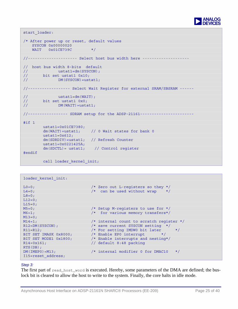
start_loader: /* After power up or reset, default values SYSCON 0x00000020 WAIT 0x01CE739C */ //--------------------- Select host bus width here -------------------- // host bus width 8-bits default // ustat1=dm(SYSCON); // bit set ustat1 0x10; // DM(SYSCON)=ustat1; //------------------ Select Wait Register for external SRAM/SBSRAM ------ // ustat1=dm(WAIT); // bit set ustat1 0x0; // DM(WAIT)=ustat1; //----------------- SDRAM setup for the ADSP-21161----------------------- #if 1 ustat1=0x01CE7380; dm(WAIT)=ustat1; // 0 Wait states for bank 0 ustat1=0x612; dm(SDRDIV)=ustat1; // Refresh Counter ustat1=0x0221425A; dm(SDCTL)= ustat1; // Control register #endif call loader_kernel_init;
loader_kernel_init: L0=0; /* Zero out L-registers so they */ L4=0; /* can be used without wrap */ L8=0; L12=0; L15=0; M5=0; /* Setup M-registers to use for */ M6=1; /* for various memory transfers*/ M13=0; M14=1; /* internal count to scratch register */ R12=DM(SYSCON); /* save current SYSCON setting */ R11=R12; /* For setting IMDW0 bit later */ BIT SET IMASK 0x8000; /* Enable EP0 interrupt */ BIT SET MODE1 0x1800; /* Enable interrupts and nesting*/ R14=0x161; // default 8:48 packing RTS(DB); DM(IMEP0)=M13; /* internal modifier 0 for DMAC10 */ I15=reset_address;
Step 3: The first part of read_host_word is executed. Hereby, some parameters of the DMA are defined; the bus-lock bit is cleared to allow the host to write to the system. Finally, the core halts in idle mode.

a
Asynchronous Host Interface on ADSP-21161N SHARC® Processors (EE-209) Page 26 of 40
read_boot_info: CALL read_HOST_word; R0=PASS R2; // stores TAG number in R0 CALL read_HOST_word; R0=PASS R0; // identify TAG number IF NE JUMP (PC, test_dm16_zero);
read_HOST_word: DM(IIEP0)=I15; /* internal index for DMAC10 */ DM(CEP0)=M14; /* internal count for DMAC10 */ DM(DMAC10)=R14; /* Start DMAC10 again */ BIT CLR MODE2 0x40; /* Clear BUSLOCK, let HOST write */ BIT CLR FLAGS FLG1; // optional command for diagnostic IDLE; /* core waits for one 48-bit word */ PX=PM(reset_address); /* Read word from scratch */ R2=PX1; /* Copy PX values into DREGS */ RTS (DB); R2=LSHIFT R2 by -16; /* adjust for the extension HH */ R2=PASS R2, R3=PX2; /* Test for boot header */
Step 4: The host initiates by writing a packed 48-bit word, which is a boot header containing a tag number. After the word is collected in the EP0I FIFO, an interrupt brings the core out of the idle. The repetitive instructions in the interrupt routine will clear the DMA channel and set the bus-lock bit to prevent bus conflicts with the host.
___lib_EP0I: BIT SET FLAGS FLG1; // optional command for diagnostic BIT SET MODE2 0x40; /* Set BUSLCK bit, lockout HOST */ R2=DM(DMAC10); /* Get DMAC Control setting */ RTI (DB); /* must be placed */ R6=R2-1; /* Clear the DMA enable bit */ DM(DMAC10)=R6; /* between uses. */
Step 5: The second part of read_host_word is now executed. The data at DMA scratch destination 0x40004 is transferred to the PX register. Next command loads the TAG number from PX to register file R2.
The steps 3-5 are done twice in order to latch the boot header: In the meantime, the TAG number is copied from R2 to R0. The 2nd call stores finally word count in R2 and start address in R3.
Step 6: The next block is responsible for boot section identification with the contents of R0. Three types of boot sections are available:
• Memory init (host writes 48-bit words)
• Memory zero (host is waiting)
• Final init (host writes IVT)

a
Asynchronous Host Interface on ADSP-21161N SHARC® Processors (EE-209) Page 27 of 40
test_pm16_init: R0=R0-1; IF EQ JUMP (PC, pm16_init); test_pm32_init: R0=R0-1; IF EQ JUMP (PC, pm32_init); test_pm40_init: R0=R0-1; IF EQ JUMP (PC, pm40_init); test_pm48_init: R0=R0-1; IF NE JUMP test_dm64_zero;
Step 7: After the kernel recognized the boot sections “memory_init” it calls read_host_word again to collect code and data until the word count has expired.
At the end, the kernel jumps back to wait for next boot section.
pm32_init: dm32_init: I0=R3; LCNTR=R2, DO dm_PM_32_init_loop UNTIL LCE; CALL read_HOST_word (DB); NOP; NOP; dm_PM_32_init_loop
Step 8: It the kernel recognizes the boot section “memory_zero”, it will start loading zeros. The host needs not to write zeros over the bus. If large arrays must be allocated, a longer time must be taken into account because the slave’s core is busy for the zeroing.
At the end, the kernel jumps back to wait for next boot section.
pm32_zero: dm32_zero: pm16_zero: dm16_zero: R0=R0-R0, I0=R3; LCNTR=R2, DO zero_loop UNTIL LCE; zero_loop: DM(I0,M6)=R0;
Step 9: The 1st word of the last boot header must contain final init; the 2nd word contains the original instruction placed at 0x40050 of user’s code (word count and start address are redundant for final init). This instruction is latched by the core’s PX-register.
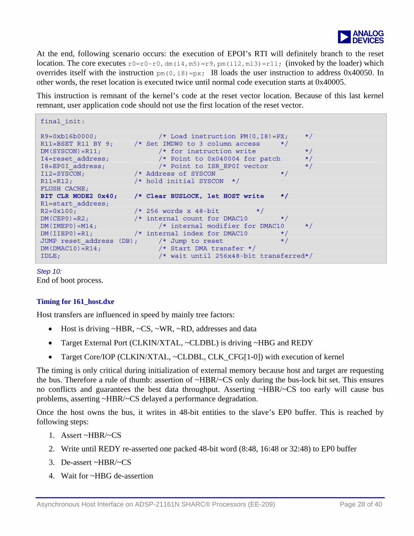
Now, final_init is executed. The original SYSCON setting is restored. Parameter registers are described for the final 256 words slave DMA, bus-lock is cleared and the cache is flushed.
Before the core is idling in a delayed branch (db), it will enable DMAC10. The host overrides the existing kernel word per word. Only location 0x40050 is forced to contain an RTI instruction (invoked by the loader).
a
Asynchronous Host Interface on ADSP-21161N SHARC® Processors (EE-209) Page 28 of 40
At the end, following scenario occurs: the execution of EPOI’s RTI will definitely branch to the reset location. The core executes r0=r0-r0,dm(i4,m5)=r9,pm(i12,m13)=r11; (invoked by the loader) which overrides itself with the instruction pm(0,i8)=px; I8 loads the user instruction to address 0x40050. In other words, the reset location is executed twice until normal code execution starts at 0x40005.
This instruction is remnant of the kernel’s code at the reset vector location. Because of this last kernel remnant, user application code should not use the first location of the reset vector.
final_init: R9=0xb16b0000; /* Load instruction PM(0,I8)=PX; */ R11=BSET R11 BY 9; /* Set IMDW0 to 3 column access */ DM(SYSCON)=R11; /* for instruction write */ I4=reset_address; /* Point to 0x040004 for patch */ I8=EP0I_address; /* Point to ISR_EP0I vector */ I12=SYSCON; /* Address of SYSCON */ R11=R12; /* hold initial SYSCON */ FLUSH CACHE; BIT CLR MODE2 0x40; /* Clear BUSLOCK, let HOST write */ R1=start_address; R2=0x100; /* 256 words x 48-bit */ DM(CEP0)=R2; /* internal count for DMAC10 */ DM(IMEP0)=M14; /* internal modifier for DMAC10 */ DM(IIEP0)=R1; /* internal index for DMAC10 */ JUMP reset_address (DB); /* Jump to reset */ DM(DMAC10)=R14; /* Start DMA transfer */ IDLE; /* wait until 256x48-bit transferred*/
Step 10: End of boot process.
Timing for 161_host.dxe
Host transfers are influenced in speed by mainly tree factors:
• Host is driving ~HBR, ~CS, ~WR, ~RD, addresses and data
• Target External Port (CLKIN/XTAL, ~CLDBL) is driving ~HBG and REDY
• Target Core/IOP (CLKIN/XTAL, ~CLDBL, CLK_CFG[1-0]) with execution of kernel
The timing is only critical during initialization of external memory because host and target are requesting the bus. Therefore a rule of thumb: assertion of ~HBR/~CS only during the bus-lock bit set. This ensures no conflicts and guarantees the best data throughput. Asserting ~HBR/~CS too early will cause bus problems, asserting ~HBR/~CS delayed a performance degradation.
Once the host owns the bus, it writes in 48-bit entities to the slave’s EP0 buffer. This is reached by following steps:
1. Assert ~HBR/~CS
2. Write until REDY re-asserted one packed 48-bit word (8:48, 16:48 or 32:48) to EP0 buffer
3. De-assert ~HBR/~CS
4. Wait for ~HBG de-assertion

a
Asynchronous Host Interface on ADSP-21161N SHARC® Processors (EE-209) Page 29 of 40
5. Wait for Bus-Lock activation
6. Repeat steps 1-5 until LDR-file’s end
Capture 7: Execution of Loader Kernel with ~HBR/~CS low during Bus-Lock set
Capture 7: The de-assertion time of ~HBR is constant and re-asserted during bus lock active.
On the left side, the kernel DMA has nearly finished. The interrupt (clears the DMAC10 and sets bus-lock) forces the sequencer to start execution of the kernel. The ~MS0 starts toggling indicating the initialization of the SDRAM controller and SDRAM. (The IO-flag does not show a bus-lock during kernel execution while the “IO-flag to output” instruction will be executed in the kernel). REDY extends the 1st write until ~HBG is low. The first two 48-bit writes the boot section header containing the TAG number, start address and the number of words. The latched TAG is compared with all reference TAGs (listing 1) until a match occurs. This scenario is dynamic and varies based on the TAG hits. Finally, the data of the boot sections are transferred. This procedure is repetitive until all sections are booted.
Capture 8: Booting of external memory
Capture 8: Booting external memory requires correct bus arbitration between host and target. This is reached if the requests fall in the bus-lock window.
Host Timeout
With the elfloader’s “-t host timeout switch”, the allocation for arrays in external memory example can be divided to sub portions by specifying a counter.

a
Asynchronous Host Interface on ADSP-21161N SHARC® Processors (EE-209) Page 30 of 40
This is helpful for some host, which may need to drive the bus frequently.
Window 3: Using “-t timeout” switch
// LDR file generated in 16-bit include format // Data order of include format: lower-, middle, and then upper-16 bits // loader generates one TAG based on t=32768 cycles (default) 0x0002, 0x0000, 0x0000, 0x0200, 0x0009, 0x0020, // loader generates six TAGs based on t=50 cycles 0x0002, 0x0000, 0x0000, 0x0065, 0x0009, 0x0020, 0x0002, 0x0000, 0x0000, 0x0065, 0x006e, 0x0020, 0x0002, 0x0000, 0x0000, 0x0065, 0x00d3, 0x0020, 0x0002, 0x0000, 0x0000, 0x0065, 0x0138, 0x0020, 0x0002, 0x0000, 0x0000, 0x0065, 0x019d, 0x0020, 0x0002, 0x0000, 0x0000, 0x0007, 0x0202, 0x0020,
Listing 3: External memory init (default vs. timeout)
Furthermore, if you allocate the boot sections for external memory with code packing x48, x32, x16, x8 bits using “.var buffer[N];” the allocation time can be extended up to eight times based on the packing mode which translates the logical to the physical array length. Additional, the user must explicitly

a
Asynchronous Host Interface on ADSP-21161N SHARC® Processors (EE-209) Page 31 of 40
set the IPACK-bits/SYSCON in the internal memory before fetching to external locations [2]. This is necessary because the loader writes the default SYSCON setting back. Next table illustrates the relations:
LDF: segment width LDR: section type Logical length Physical length
48-bit 0x1A zero pm48 ext N N
32-bit 0x19 zero pm32 ext N 2*N
16-bit 0x18 zero pm16 ext N 4*N
8-bit 0x17 zero pm8 ext N 8*N
Table 8: Logical versus physical addresses
Capture 9: External Memory Zero Init with timeout disabled
Capture 9 shows the allocation of external memory. Hereby, the bus-lock is active during the whole time.
Capture 10: External Memory Zero Init using timeout=50 cycles
Capture 10 illustrates the timeout feature activated by the loader options. The initialization of external memory is simply divided in sub portions to make sure that the host can drive the bus from time to time based on the counter.

a
Asynchronous Host Interface on ADSP-21161N SHARC® Processors (EE-209) Page 32 of 40
64-bit Boot Sections
Long word boot sections have exceptional handling: To init a long word (64-bit) the host needs to write two times to the EP0 buffer because of the 32-bit bus. If a buffer is to be declared in long word “.var buffer_64[N]=data.dat;” the buffer allocation in long-word (64-bits) memory must be a multiple of 2, otherwise the loader will return an error message.
General Steps for Booting
1. Select Project Options “Load”, select a kernel and define options (window 2)
2. Select Project Options “Type” “DSP loader file” (window 1)
3. Compile to get a LDR-file
4. Invoke the LDR-file in the host program
5. Host arbitrates for the bus and writes LDR-file at the address of the slave’s EP0 buffer
6. DSP starts execution
Loader Kernel Customization
Of course you can modify the kernel to your needs. Analog Devices provides a default boot loader kernel source file with the VisualDSP++ development tools, 161_host.asm and 161_ldr.ldf. You have to invoke 161_host.asm and 161_ldr.ldf in a project to build the new reference executable.
Main reasons to change the boot kernel are:
• Host bus width (HBW-bits/SYSCON)
• DMA packing mode (PMODE-bits/DMAC10)
• Host Word order (HMSWF-bit/ SYSCON)
• DMA Word order (MSWF-bit/DMAC10)
• Wait -mode and -states (EBxAM and EBxWS-bits/WAIT) SRAM/SBSRAM/SDRAM
• SDRAM control (SDRDIV, SDCTL)
Example 1: 8-bit (default) transfer required. No modifications are necessary regarding bus width and data packing. Host must write only to the EP0 buffer. Example 2: For 16 and 32-bit bus width, host should write to SYSCON and DMAC10 directly before booting. Of course, the kernel must also match with the host’s modifications.

a
Asynchronous Host Interface on ADSP-21161N SHARC® Processors (EE-209) Page 33 of 40
IOP-register DMAC10 SYSCON
Host-Packing PMODE-bits HBW-bits
8:48 5 (default) 2 (default)
16:48 2 1
32:48 3 0
Table 9: Basic host settings
It is very important to check the address of __lib_EP0I after a kernel modification, the RTI instruction must be placed after 0x40050.
Boot Timing DSP with External Memory
Capture 11: It shows the timing of the entire boot process, which contains basically 4 stages: the 1st stage writes to the SRST-bit/SYSCON and ADREDY-bit/SYSCON. The 2nd stage writes the kernel into the DSP. The 3rd stage executes the kernel and loads the application into internal/external memory. The 4th stage overrides the remaining IVT into the DSP where the DSP starts after final init code execution. During all stages, ~HBR is asserted for each 48-bit word. In this case, the boot process needs ≈ 480µs.
Capture 11: Entire host boot procedure: ~HBR toggling for each word
Capture 12: It shows the same entire boot process. Loading the kernel and final init, ~HBR is continuously asserted. In this way, boot speed is easily increased to ≈ 340µs.
Capture 12: Entire host boot procedure: ~HBR during DMAs asserted

a
Asynchronous Host Interface on ADSP-21161N SHARC® Processors (EE-209) Page 34 of 40
Both ways are valid. It is not expected that the DSP de-asserted ~HBG while the 256 words DMA of the kernel are booted in. Therefore, the timing for this boot section is optional. This is also valid for the final init DMA.
Booting C/C++ Programs
Booting a C/C++ program uses the same timing compared to an assembler based programs. But some differences are based on the boot sections: The run time environment requires a default internal memory map realized with the “memory ” command in the standard LDF-file. This is necessary because the loader invokes the run time environment [6].
// required internal memory segments for a C-program MEMORY seg_rth TYPE(PM RAM) START(0x00040000) END(0x000400ff) WIDTH(48) // interrupt table, ISR seg_init TYPE(PM RAM) START(0x00040100) END(0x000401ff) WIDTH(48) // loader for system init data seg_pmco TYPE(PM RAM) START(0x00040200) END(0x000419ff) WIDTH(48) // user code, run time library seg_pmda TYPE(PM RAM) START(0x00042700) END(0x00043fff) WIDTH(32) // data block 0, run time library seg_dmda TYPE(DM RAM) START(0x00050000) END(0x00051fff) WIDTH(32) // data block 1, run time library seg_heap TYPE(DM RAM) START(0x00052000) END(0x00052fff) WIDTH(32) // run time heap seg_stak TYPE(DM RAM) START(0x00053000) END(0x00053fff) WIDTH(32) // run time stack
Listing 4: LDF-file containing the different memory sections for C program
Next LDR-file shows the output of the loader for a C based blink program:
// LDR file generated in 16-bit include format // Data order of include format: lower-, middle, and then upper-16 bits 0x0000, 0x0000, 0x0000, // loader kernel at 0x40000 0x0000, 0x0000, 0x0000, 0x0000, 0x0000, 0x0000, 0x0000, 0x0000, 0x0000, //loader kernel at 0x400ff 0x000e, 0x0000, 0x0000, //.section/pm seg_init; (system init data) 0x0009, 0x0100, 0x0004, 0x000e, 0x0000, 0x0000, //.section/pm seg_pmco;(user code & run time library) 0x0173, 0x0200, 0x0004, 0x0002, 0x0000, 0x0000, //.section/dm seg_dmda; (run time library) 0x011e, 0x0002, 0x0005, 0x0000, 0x0000, 0x0000, //.section/pm seg_rth; (init code & interrupt table) 0x1000, 0x0000, 0x1422, 0x0000, 0x0000, 0x0000, // 0x400ff
Listing 5: LDR-file containing the different boot sections for C program

a
Asynchronous Host Interface on ADSP-21161N SHARC® Processors (EE-209) Page 35 of 40
Multi-processor Booting
Elfloader Utility
The generation of loader files is different for Multiprocessing: The executables (DXE-files) are only built simultaneously on an existing LDF “Processor” command (listing 6). But the elfloader does only accept one executable at its input (except for EPROM MP-booting) to make a loader boot file (LDR-file). The workaround is by controlling the utility over the command line switches by a batch file and not with the dialog box. In this case all boot files are generated sequentially over the command line. (LDR-files). So, it is not necessary to build up to 6 uni-processor projects to build loader files.
// LDF with a dual cluster DSP and shared memories ARCHITECTURE(ADSP-21161) MEMORY mem_rth TYPE(PM RAM) START(0x00040000) END(0x000400ff) WIDTH(48) // block 0 mem_init TYPE(PM RAM) START(0x00040100) END(0x000401ff) WIDTH(48) mem_pmco TYPE(PM RAM) START(0x00040200) END(0x000419ff) WIDTH(48) mem_pmda TYPE(PM RAM) START(0x00042700) END(0x00043fff) WIDTH(32) mem_dmda TYPE(DM RAM) START(0x00050000) END(0x00053fff) WIDTH(32) // block 1 mem_bk01 TYPE(DM RAM) START(0x00200000) END(0x00200fff) WIDTH(32) // bank 0 mem_bk02 TYPE(DM RAM) START(0x00201000) END(0x00201fff) WIDTH(32) MPMEMORY // multi-processor offset definition ID1 START(0x00100000) ID2 START(0x00120000) SHARED_MEMORY // Shared memory 1 definition OUTPUT(shared_1.sm) SECTIONS dxe_bk01 INPUT_SECTIONS( shared_1.doj(seg_bk01) ) >mem_bk01 SHARED_MEMORY // Shared memory 2 definition OUTPUT(shared_2.sm) SECTIONS dxe_bk02 INPUT_SECTIONS( shared_2.doj(seg_bk02) ) >mem_bk02 PROCESSOR ID1 // Processor ID1 sections definition.

a
Asynchronous Host Interface on ADSP-21161N SHARC® Processors (EE-209) Page 36 of 40
LINK_AGAINST(shared_1.sm, shared_2.sm, ID2.dxe) OUTPUT(ID1.dxe) SECTIONS dxe_rth INPUT_SECTIONS( IVT_ID1.doj(seg_rth) ) >mem_rth dxe_init INPUT_SECTIONS( ID1.doj(seg_init) ) >mem_init dxe_pmco INPUT_SECTIONS( ID1.doj(seg_pmco) ) >mem_pmco dxe_pmda INPUT_SECTIONS( ID1.doj(seg_pmda) ) >mem_pmda dxe_dmda INPUT_SECTIONS( ID1.doj(seg_dmda) ) >mem_dm PROCESSOR ID2 // Processor ID2 sections definition. LINK_AGAINST(shared_1.sm, shared_2.sm, ID1.dxe) OUTPUT(ID2.dxe) SECTIONS dxe_rth INPUT_SECTIONS( IVT_ID2.doj(seg_rth) ) >mem_rth dxe_init INPUT_SECTIONS( ID2.doj(seg_init) ) >mem_init dxe_pmco INPUT_SECTIONS( ID2.doj(seg_pmco) ) >mem_pmco dxe_pmda INPUT_SECTIONS( ID2.doj(seg_pmda) ) >mem_pmda dxe_dmda INPUT_SECTIONS( ID2.doj(seg_dmda) ) >mem_dmda
Listing 6: LDF-file for multiprocessor system

a
Asynchronous Host Interface on ADSP-21161N SHARC® Processors (EE-209) Page 37 of 40
Shared Memory
Shared memories (SM) files are only built on an existing LDF “Shared Memory” command. The loader accepts also multiple shared memories as input. If system uses shared memory, every boot target would contain the shared memory boot section in its LDR-file. With the help of the elfloader’s switch “–e except shared memory”, the user can omit the shared memory boot section for every boot target optional in order to save size and system performance.
// Command Line Processor 1 elfloader.exe .\Processor_1.dxe -bhost -finclude -l "C:\path\161_host.dxe" -HostWidth 16 -o .\loader\blink_1.ldr -t32786 -proc ADSP-21161 // Command Line Processor 2 elfloader.exe.\Processor_2.dxe -bhost -finclude -l "C:\path\161_host.dxe" -HostWidth 16 -o .\loader\blink_2.ldr -t32786 -proc ADSP-21161 -e shared_1.sm -e shared_2.sm
Listing 7: Batch file for MP-booting
Boot Timing Cluster DSP with Shared Memory
Capture 13: The boot sequence is exactly the same like for uni-processor systems, the host must sequentially boot the targets with ~HBR/~CS1 and ~HBR/~CS2.
The Vector Interrupt IOP-register (capture 14) in conjunction with broadcast write allows one possibility of simultaneous execution of the booted targets. Listing 8 shows how to place instructions in the user’s IVT. After the single DSPs are booted, they will remain in that endless loop. Now, the host initiates a broadcast write to VIRPT-register (capture 16), which starts cluster execution [2].
// processor_1 ___lib_RSTI: NOP; // reset address 0x40004 bit set IMASK VIRPTI; // enable VIRPTI jump (pc,0); // endless loop jump start_1; // VIRPT points to here // processor_2 ___lib_RSTI: NOP; // reset address 0x40004 bit set IMASK VIRPTI; // enable VIRPTI jump (pc,0); // endless loop jump start_2; // VIRPT points to here
Listing 8: VIRPT accesses

a
Asynchronous Host Interface on ADSP-21161N SHARC® Processors (EE-209) Page 38 of 40
Capture 13: Entire host dual multi-processor boot procedure
Capture 14: Broadcast write to VIRPT register starts execution in dual multi-processor system
Debug Issues
Modification of LDR-file
The user can change the ranking of various boot sections (listing 2) in the LDR-file to its own need. Only two restrictions must be followed:
• Host kernel must be placed at the first 256 locations
• Final init must be placed at the end of the LDR-file
Booting without Loader Kernel
An easy test to check the hardware is given to boot the DSP without the loader kernel by using a simple blink program. Open the LDR-file and delete the kernel and the final init (first and last 256 words). This will now place your code into the IVT. Important: execution needs the RTI instruction at address 0x40050. By asserting ~HBR and ~CS low and writing to EP0 buffer, the LED must finally start toggling indicating a functional hardware.

a
Asynchronous Host Interface on ADSP-21161N SHARC® Processors (EE-209) Page 39 of 40
// manually generated LDR-file in 16-bit include format // Data order of include format: lower-, middle, and then upper-16 bits // place NOPs until 0x40004 0x0000, 0x0000, 0x0000, // 0x40000 0x0000, 0x0000, 0x0000, 0x0000, 0x0000, 0x0000, 0x0000, 0x0000, 0x0000, 0x0000, 0x0000, 0x0000, 0x0000, 0x0002, 0x1404, // 0x40005 start of blink program 0x0004, 0x0000, 0x1425, 0x0000, 0x0000, 0x0000, 0x000d, 0x0004, 0x063e, // end of blink program 0x0000, 0x0000, 0x0000, 0x0000, 0x0000, 0x0000, 0x0000, 0x0000, 0x0b3e, // RTI instruction at 0x40050 0x0000, 0x0000, 0x0000, 0x0000, 0x0000, 0x0000, // 0x400ff
Listing 9: Generation of LDR-file without loader kernel
Steps for Diagnostic
There could be some reasons why booting fails: Host booting requires two independent driven timings of host and the slave with different speeds based on the asynchronous nature. Therefore, it is useful to provide additional information during the boot process by placing IO-Flags at dedicated places in the kernel’s source file (161_host.asm). It will ensure that the slave’s core is executing like expected or not. Extremely useful locations for debug are read_host_word and __lib_EP0I by placing the IO-Flag close to the bus-lock instructions bit set mode2 BUSLK; and bit clr mode2 BUSLK;. The IO-Flag is simply sampled as a “bus-lock indicator” as shown in the captures 9-11. With this diagnostic method, it is easier to control handshake (bus conflicts) or to improve system performance.
Emulation Issues
Debugging a host system needs the understanding between user space (Run/F5) and emulation space (Halt/Shift F5). Starting the emulator under session generates first an external interrupt (highest priority at address 0x40000) via JTAG interface to the DSP (~TRST = high) and enters the part immediately into emulation space. Hereby, the core is halted and controlled by the debug software for updating the graphical user interface. Hardware and software breakpoints will also force an emulator interrupt. Pushing Run/F5 will leave emulation space by scanning an RTI instruction via JTAG to the DSP (return from interrupt). Now the core is in Run mode (user space).
DMA activities The IOP is handled differently during emulation space. Based on target options, the IOP will halt or continue if the core enters emulation space triggered by a breakpoint. To debug the loader kernel and final init DMA, start an emulation session. The core remains halt. With the host debug tools, write in single
a
Asynchronous Host Interface on ADSP-21161N SHARC® Processors (EE-209) Page 40 of 40
step word per word into the FIFO. With refresh/F12, the window refresh occurs and you can follow all the instruction written into IVT. With the DMA Addressing window, you can follow the decrementing of the CEP0 counter until DMAC10 has finished.
Core activities To debug slave’s core activities, place a breakpoint at the idle; instruction in read_host_word. Push Run/F5 to execute the kernel, the DMA status shows the CEP0=1 to expect the boot tag number after the kernel is loaded down. Now, the host must write the first word to the EP0 buffer. After done, push refresh/F12. The CEP0 counter decrements to zero again indicating a new 48-bit word to be collected at the reset address 0x40004. Push Run/F5 to execute the kernel, the DMA status shows the CEP0=1 to expect the next word. This scenario is repetitive until the user’s code is drawn down into the DSP target.
Entire boot scenario The entire boot process requires the slave’s core and DMA activities. Therefore it is necessary to run the slave into user space.
References [1] ADSP-21161N SHARC DSP Microcomputer Datasheet. Rev A, May 2003, Analog Devices Inc.
[2] ADSP-21161 SHARC Processor Hardware Reference. Rev 4.0, February 2005, Analog Devices Inc.
[3] 74LV245 Octal bus transceiver (3-State) Datasheet. April 1998, Philips Semiconductors
[4] ADSP-21065L SHARC DSP Microcomputer Datasheet. Rev C, June 2003, Analog Devices Inc.
[5] VisualDSP++ 5.0 Linker and Utilities Manual. Rev 3.0, August 2007, Analog Devices Inc.
[6] VisualDSP++ 5.0 C/C++ Compiler Manual for SHARC Processors. Rev 1.0, August 2007, Analog Devices Inc.
Document History
Revision Description
Rev 2 – September 5, 2007 by Robert Hoffmann
Updated Timing Requirements section, as well as some general formatting issues
Rev 1 – September 23, 2003 by Robert Hoffmann
Initial release


![[XLS] · Web view28 209 70227595 29 209 70775496 30 209 70554395 31 209 70775195 32 209 70559596 33 209 70774296 34 209 70778999 35 209 70773995 36 209 70226095 37 209 70776596 38](https://img.pdfslide.us/doc/110x75/5b0cded17f8b9ab7658b981b/xls-view28-209-70227595-29-209-70775496-30-209-70554395-31-209-70775195-32-209.jpg)