Embed Size (px)
Citation preview
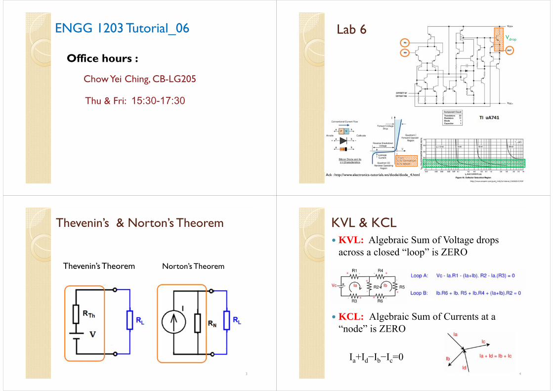
ENGG 1203 Tutorial_06
Office hours :
Chow Yei Ching, CB-LG205
Thu & Fri: 15:30-17:30
Lab 6
2Ack : http://www.electronics-tutorials.ws/diode/diode_4.html
Vdrop
Thevenin’s & Norton’s Theorem
3
Thevenin’s Theorem Norton’s Theorem
KVL & KCL KVL: Algebraic Sum of Voltage drops
across a closed “loop” is ZERO
4
KCL: Algebraic Sum of Currents at a “node” is ZERO
Ia+Id−Ib−Ic=0
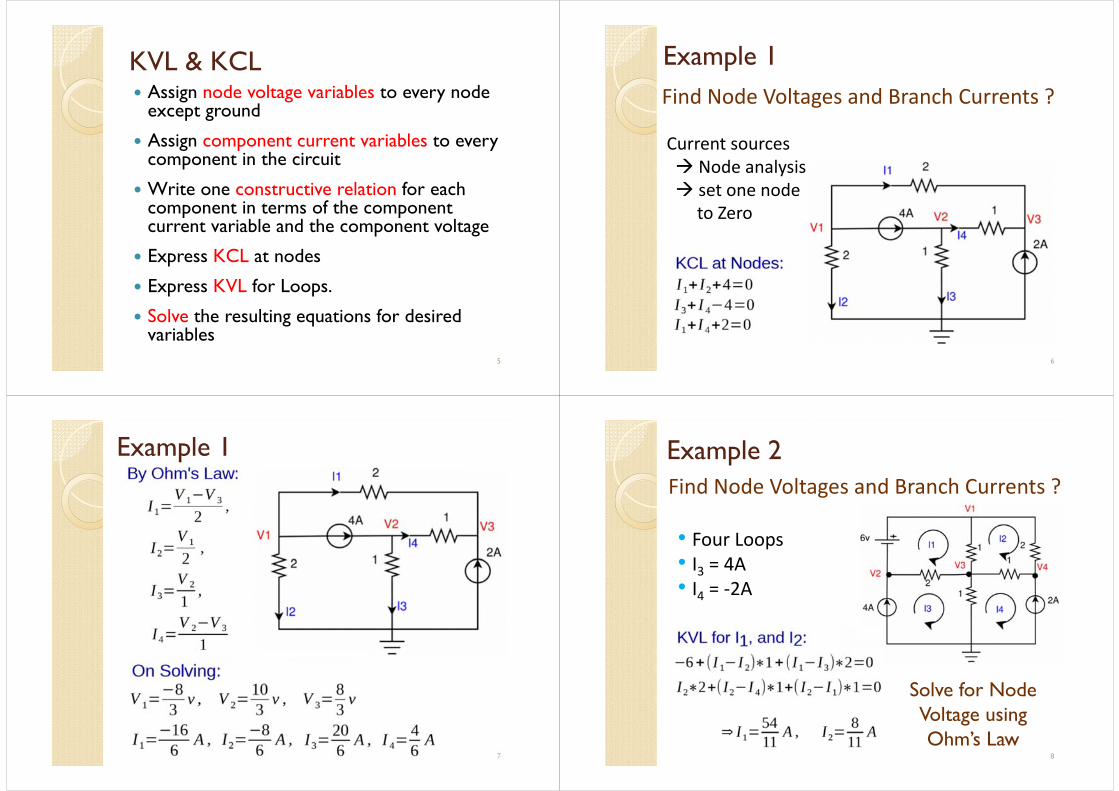
KVL & KCL Assign node voltage variables to every node
except ground
Assign component current variables to every component in the circuit
Write one constructive relation for each component in terms of the component current variable and the component voltage
Express KCL at nodes
Express KVL for Loops.
Solve the resulting equations for desired variables
5
Example 1
6
Find Node Voltages and Branch Currents ?
Current sources Node analysis set one node
to Zero
Example 1
7
Example 2
8
Find Node Voltages and Branch Currents ?
• Four Loops • I3 = 4A• I4 = ‐2A
Solve for Node Voltage using Ohm’s Law
V3 = (I3-I4) *1= (4-(-2))* 1 = 6V
9
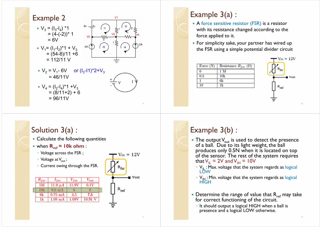
Example 2
V1= (I1-I2)*1 + V3= (54-8)/11 +6= 112/11 V
V2 = V1- 6V or (I3-I1)*2+V3= 46/11V
V4 = (I2-I4)*1 +V3= (8/11+2) + 6 = 96/11V
A force sensitive resistor (FSR) is a resistor with its resistance changed according to the force applied to it.
For simplicity sake, your partner has wired up the FSR using a simple potential divider circuit
10
Example 3(a) :
11
Solution 3(a) : Calculate the following quantities when Rref = 10k ohm : Voltage across the FSR ; Voltage at Vout ; Current owing through the FSR.
12
Example 3(b) : The output Vout is used to detect the presence
of a ball. Due to its light weight, the ball produces only 0.5N when it is located on top of the sensor. The rest of the system requires that VIL = 2V and VIH = 10V VIL : Max. voltage that the system regards as logical
LOW VIH : Min. voltage that the system regards as logical
HIGH
Determine the range of value that Rref may take for correct functioning of the circuit. It should output a logical HIGH when a ball is
presence and a logical LOW otherwise.
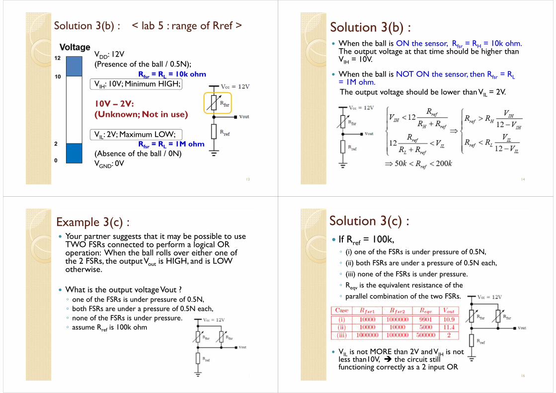
Solution 3(b) : < lab 5 : range of Rref >
VDD: 12V (Presence of the ball / 0.5N);
Rfsr = RL = 10k ohmVIH: 10V; Minimum HIGH;
10V – 2V: (Unknown; Not in use)
VIL: 2V; Maximum LOW; Rfsr = RL = 1M ohm
(Absence of the ball / 0N) VGND: 0V
13
Solution 3(b) : When the ball is ON the sensor, Rfsr = RH = 10k ohm.
The output voltage at that time should be higher than VIH = 10V.
When the ball is NOT ON the sensor, then Rfsr = RL= 1M ohm. The output voltage should be lower than VIL = 2V.
14
Example 3(c) : Your partner suggests that it may be possible to use
TWO FSRs connected to perform a logical OR operation: When the ball rolls over either one of the 2 FSRs, the output Vout is HIGH, and is LOW otherwise.
What is the output voltage Vout ? one of the FSRs is under pressure of 0.5N, both FSRs are under a pressure of 0.5N each, none of the FSRs is under pressure. assume Rref is 100k ohm
15
Solution 3(c) : If Rref = 100k, (i) one of the FSRs is under pressure of 0.5N, (ii) both FSRs are under a pressure of 0.5N each, (iii) none of the FSRs is under pressure. Reqv is the equivalent resistance of the parallel combination of the two FSRs.
16
VIL is not MORE than 2V and VIH is not less than10V, the circuit still functioning correctly as a 2 input OR

If there are THREE FSRs connected in parallel, assume Rref remains at 100k
THEN, will it behave as a 3-input OR?
17
Solution 3(d) :
NOT, because Vout > 2 V
Solution 3 : Yes, it works correctly as a 2-input OR gate
because the output is HIGH when there is a ball on top of at least one of the input.
If we connect THREE FSRs in parallel, the circuit CANNOT correctly function as a 3-input OR gate. In the case when there is no ball falling on the circuit, the
equivalent resistance of the parallel combination of the THREE FSRs drops too low, which give a Vout > 2V .
As a result, the output FAILED to represent a logical LOW in this case.A new R’ref is needed
18
Operational Amplifier
19
Package : TO CANDIP or DILSurface Mount…
Technology : Material, process,machines
http://www.righto.com/2015/10/inside-ubiquitous-741-op-amp-circuits.html
IC Chip : Si, Al, oxide..
Technology : IC processes
Where to make the Chips
20http://hexus.net/business/news/components/107617-micron-dram-factory-mishap-taiwan-results-fab-suspension/http://download.intel.com/newsroom/kits/chipmaking/pdfs/Sand-to-Silicon_32nm-Version.pdf
FROM SAND Circuit Design Fabrication Process Package Design
Sand to Circuit (https://www.youtube.com/watch?v=Q5paWn7bFg4)Fabrication (https://www.youtube.com/watch?v=-KTKg0Y1snQ)
FROM Circuit System Smart machine, TV, computer, iPAD, …..
Whatever
https://www.youtube.com/watch?v=sZ_-yb-TN9MMachine https://www.youtube.com/watch?v=-7xvqQeoA8c
Factory
https://www.youtube.com/watch?v=d9SWNLZvA8g
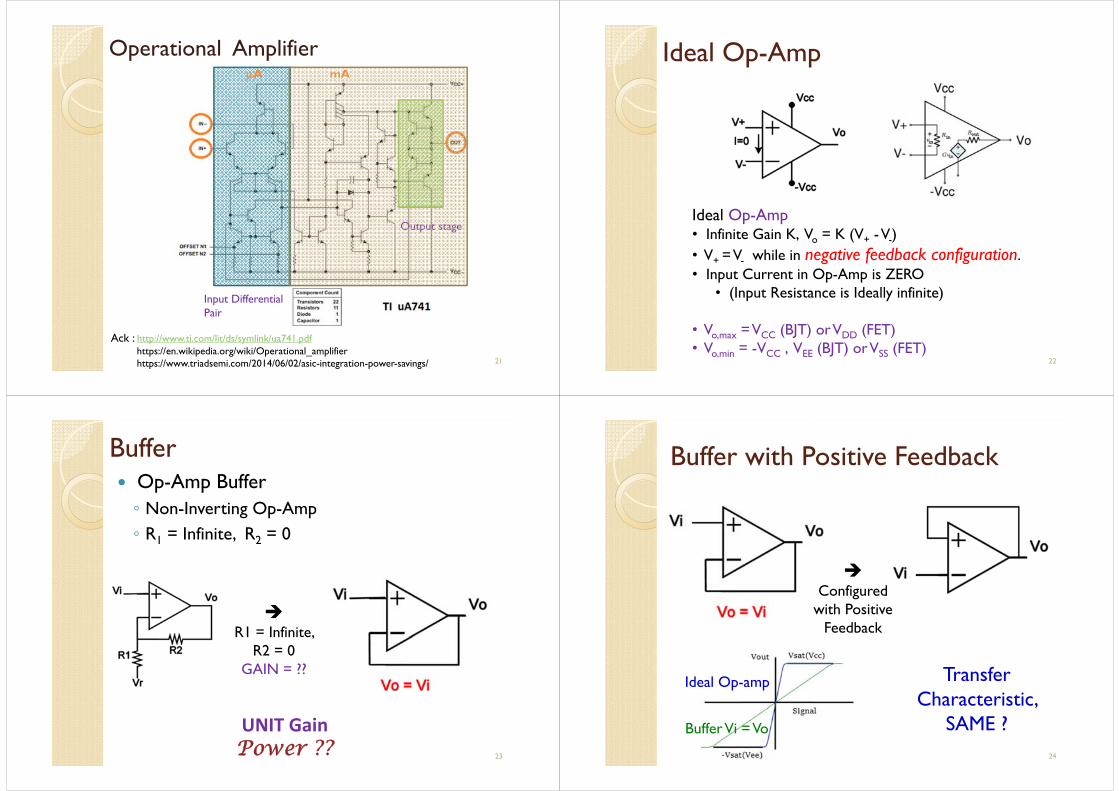
Operational Amplifier
21
Ack : http://www.ti.com/lit/ds/symlink/ua741.pdfhttps://en.wikipedia.org/wiki/Operational_amplifierhttps://www.triadsemi.com/2014/06/02/asic-integration-power-savings/
Input Differential Pair
Output stage
A mAIdeal Op-Amp
22
Ideal Op-Amp• Infinite Gain K, Vo = K (V+ -V-) • V+ = V- while in negative feedback configuration.• Input Current in Op-Amp is ZERO
• (Input Resistance is Ideally infinite)
• Vo,max = VCC (BJT) or VDD (FET) • Vo,min = -VCC , VEE (BJT) or VSS (FET)
Buffer Op-Amp Buffer Non-Inverting Op-Amp R1 = Infinite, R2 = 0
23
R1 = Infinite,
R2 = 0GAIN = ??
UNIT GainPower ??
Buffer with Positive Feedback
24
Configured
with Positive Feedback
Transfer Characteristic,
SAME ?
Ideal Op-amp
Buffer Vi = Vo
Example 1Find Out Vo ?
25
Vcc
Vee
VO,max = Vcc =12V ??,
+ & -V could be not equal ??
e.g. Vee = 0V (GND), -5V, …..
VO=K(V+−V−) VO=100000 0.001 VO=100V ????
Example 2 Students Kim, Pat, Jody, Chris, and Leon are trying
to design a controller for a display of three robotic mice in the Rube Goldberg Machine, using a 10V power supply and three motors.
The first is supposed to spin as fast as possible (in one direction only)
The second at half of the speed of the first, and
The third at half of the speed of the second.
Assume the motors have a resistance of approximately 5Ω and that rotational speed is proportional to voltage.
For each design, indicate the voltage across each of the motors.
26
Example 2a (Jody’s Design)
P.D. of motor 1 = 10V P.D. of motor 2 = 0.05V P.D. of motor 3 = 0V
27
5
Eq. R. (Red): 1K+~5 1K Eq. R. (Blue): 1K//1K//5 ~5
Wrong design
Example 2b (Chris’s Design)
P.D. of motor 1 = 10V P.D. of motor 2 = 0.45V P.D. of motor 3 = 0V
28
Wrong design
Eq. R. (Red): 100K+~5 100K Eq. R. (Blue): 100//100K//5 ~5
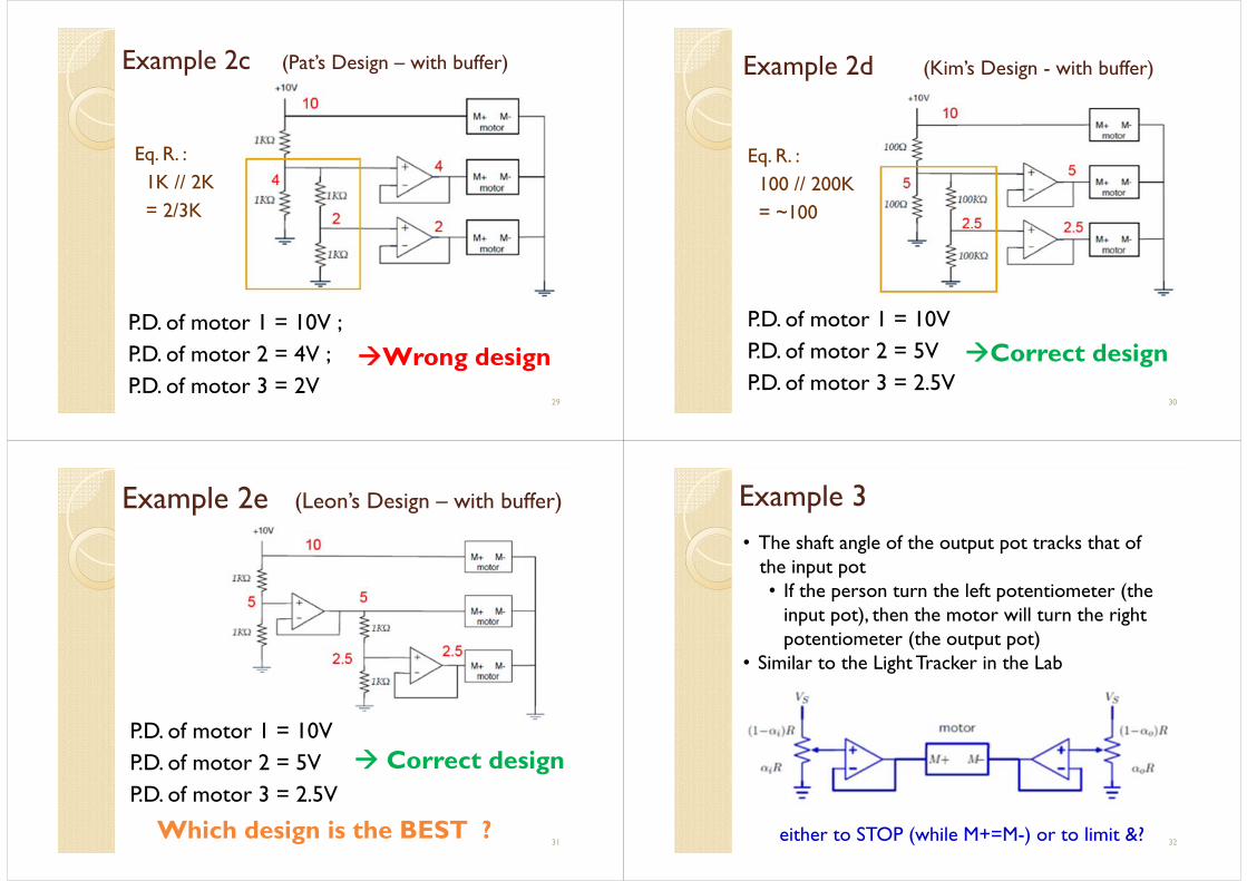
Example 2c (Pat’s Design – with buffer)
P.D. of motor 1 = 10V ;P.D. of motor 2 = 4V ;P.D. of motor 3 = 2V
29
Wrong design
Eq. R. : 1K // 2K = 2/3K
Example 2d (Kim’s Design - with buffer)
P.D. of motor 1 = 10V P.D. of motor 2 = 5VP.D. of motor 3 = 2.5V
30
Correct design
Eq. R. : 100 // 200K = ~100
Example 2e (Leon’s Design – with buffer)
Correct design
31Which design is the BEST ?
P.D. of motor 1 = 10V P.D. of motor 2 = 5VP.D. of motor 3 = 2.5V
32
Example 3• The shaft angle of the output pot tracks that of
the input pot • If the person turn the left potentiometer (the
input pot), then the motor will turn the right potentiometer (the output pot)
• Similar to the Light Tracker in the Lab
either to STOP (while M+=M-) or to limit &?
33
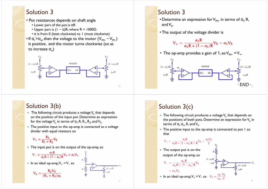
Solution 3• Pot resistances depends on shaft angle
• Lower part of the pot is αR• Upper part is (1 − α)R, where R = 1000Ω. • α is from 0 (least clockwise) to 1 (most clockwise)
• If αi >αo, then the voltage to the motor (VM+ −VM−) is positive, and the motor turns clockwise (so as to increase αo)
• The output of the voltage divider is
Solution 3
34
• Determine an expression for VM+ in terms of αi, R, and VS.
V+
- END -
• The op-amp provides a gain of 1, so VM+ = V+.
Solution 3(b) The following circuit produces a voltage Vo that depends
on the position of the input pot. Determine an expression for the voltage Vo in terms of αi, R, R1, R2, and VS.
The positive input to the op-amp is connected to a voltage divider with equal resistors so
The input pot is on the output of the op-amp, so
In an ideal op-amp, V+ = V− so
35
Solution 3(c) The following circuit produces a voltage Vo that depends on
the positions of both pots. Determine an expression for Vo in terms of αi, αo, R, and VS.
The positive input to the op-amp is connected to pot 1 so that
The output pot is on the output of the op-amp, so
In an ideal op-amp, V+ = V− so 36
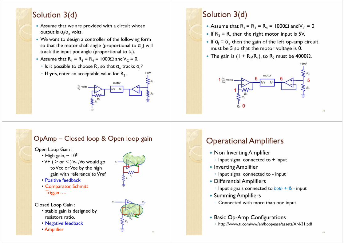
Solution 3(d) Assume that we are provided with a circuit whose
output is αi/αo volts. We want to design a controller of the following form
so that the motor shaft angle (proportional to αo) will track the input pot angle (proportional to αi).
Assume that R1 = R3 = R4 = 1000Ω and VC = 0. Is it possible to choose R2 so that αo tracks αi ? If yes, enter an acceptable value for R2.
Solution 3(d) Assume that R1 = R3 = R4 = 1000Ω and VC = 0 If R3 = R4 then the right motor input is 5V. If αi = αo then the gain of the left op-amp circuit
must be 5 so that the motor voltage is 0. The gain is (1 + R2/R1), so R2 must be 4000Ω.
38
OpAmp – Closed loop & Open loop gain
39
Open Loop Gain : • High gain, ~ 105
•V+ ( > or < ) V- , Vo would goto Vcc or Vee by the highgain with reference to Vref
• Positive feedback• Comparator, Schmitt
Trigger….
Closed Loop Gain : • stable gain is designed by
resistors ratio.• Negative feedback• Amplifier
Operational Amplifiers Non Inverting Amplifier Input signal connected to + input
Inverting Amplifier Input signal connected to - input
Differential Amplifiers Input signals connected to both + & - input
Summing Amplifiers Connected with more than one input
Basic Op-Amp Configurations http://www.ti.com/ww/en/bobpease/assets/AN-31.pdf
40
41
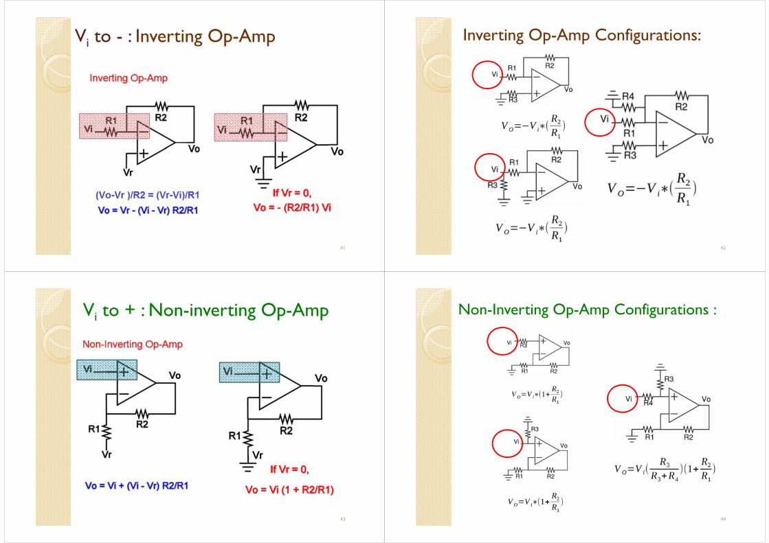
Vi to - : Inverting Op-Amp Inverting Op-Amp Configurations:
42
Vi to + : Non-inverting Op-Amp
43
Non-Inverting Op-Amp Configurations :
44
45
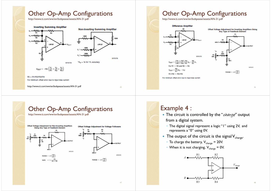
Other Op-Amp Configurationshttp://www.ti.com/ww/en/bobpease/assets/AN-31.pdf
http://www.ti.com/ww/en/bobpease/assets/AN-31.pdf 46
Other Op-Amp Configurationshttp://www.ti.com/ww/en/bobpease/assets/AN-31.pdf
47
Other Op-Amp Configurationshttp://www.ti.com/ww/en/bobpease/assets/AN-31.pdf The circuit is controlled by the “charge” output
from a digital system. The digital signal represent a logic “1” using 2V, and
represents a “0” using 0V.
The output of the circuit is the signal Vcharge. To charge the battery, Vcharge = 20V. When it is not charging, Vcharge = 0V.
48
Example 4 :
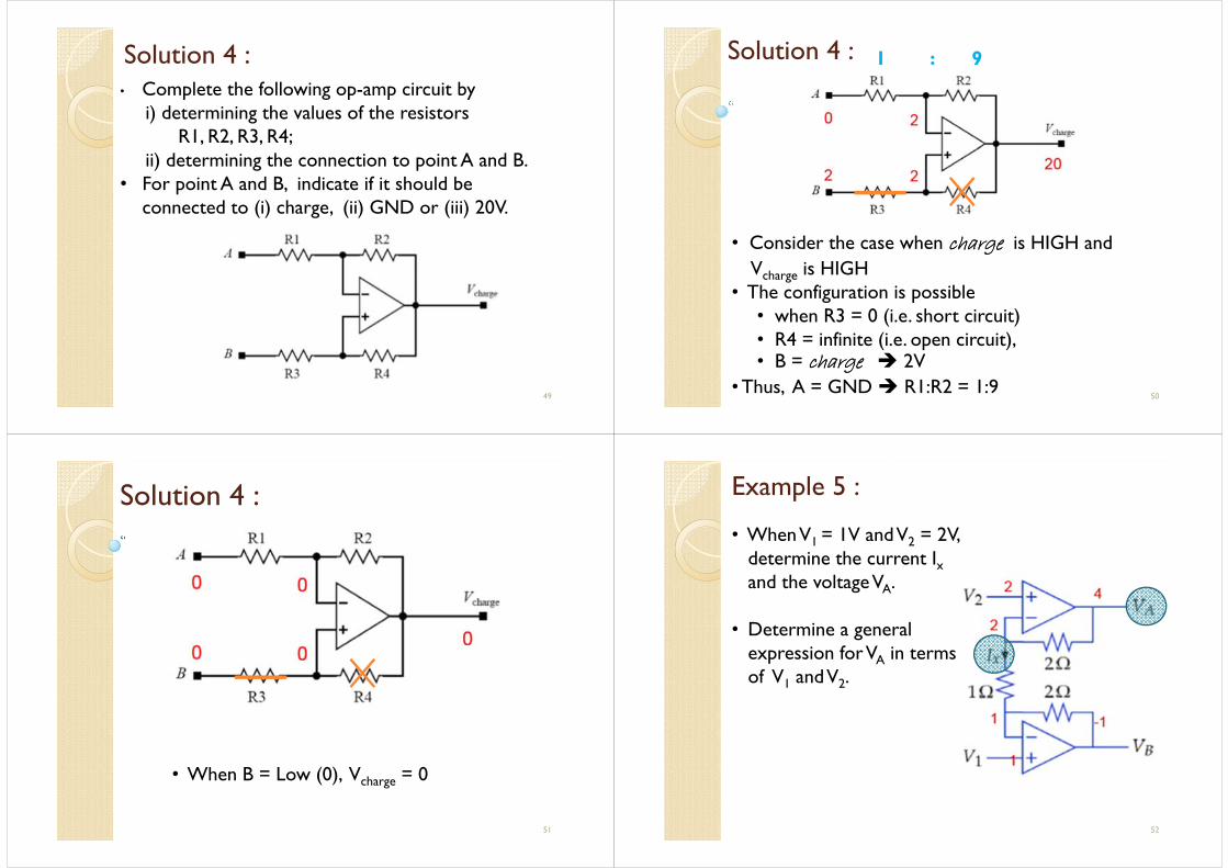
Solution 4 :
49
• Complete the following op-amp circuit byi) determining the values of the resistors
R1, R2, R3, R4; ii) determining the connection to point A and B.
• For point A and B, indicate if it should be connected to (i) charge, (ii) GND or (iii) 20V.
50
Solution 4 :
• Consider the case when charge is HIGH andVcharge is HIGH
• The configuration is possible • when R3 = 0 (i.e. short circuit) • R4 = infinite (i.e. open circuit), • B = charge 2V
• Thus, A = GND R1:R2 = 1:9
1 : 9
Solution 4 :
51
• When B = Low (0), Vcharge = 0
Example 5 :
52
• When V1 = 1V and V2 = 2V, determine the current Ixand the voltage VA.
• Determine a generalexpression for VA in termsof V1 and V2.
53
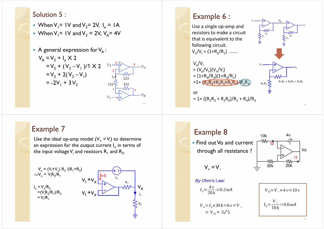
When V1= 1V and V2= 2V, Ix = 1A When V1= 1V and V2 = 2V, VA= 4V
A general expression for VA : VA = V2 + Ix X 2
= V2 + ( V2 –V1 )/1 X 2= V2 + 2( V2 –V1) = -2V1 + 3 V2
Solution 5 : Example 6 :
54
Vo/Vi= (Vo/Vn)(Vn/Vi)= (1+R4/R3)(1+R2/R1)=1+ (R1R4+R2R3+R2R4)/R1R3
or = 1+ ((R2R3 + R2R4)/R1 + R4)/R3
Use a single op‐amp and resistors to make a circuit that is equivalent to the following circuit. Vn/Vi = (1+R2/R1) …….
Example 7Use the ideal op-amp model (V+ = V-) to determine an expression for the output current Io in terms of the input voltage Vi and resistors R1 and R2.
Vx = (Vi+Vx) R2 /(R1+R2)Vx = ViR2/R1
Io = Vx/R2=(ViR2/R1)/R2= Vi/R1
Example 8 Find out Vo and current
through all resistance ?
V+ = V−
56
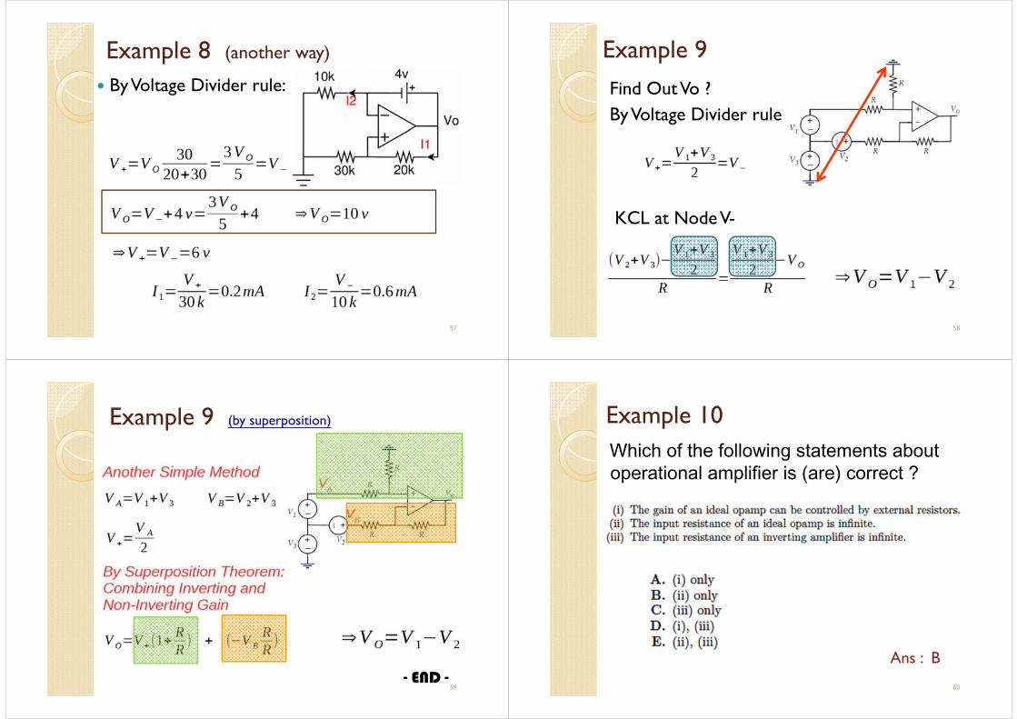
Example 8 (another way)
By Voltage Divider rule:
57
Example 9Find Out Vo ? By Voltage Divider rule :
KCL at Node V-
58
Example 9 (by superposition)
59- END -
Example 10Which of the following statements about operational amplifier is (are) correct ?
60
Ans : B
61
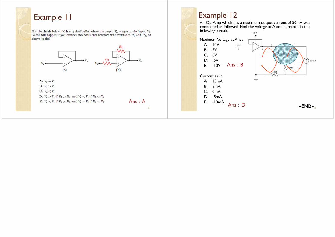
Example 11
Ans : A
An Op-Amp which has a maximum output current of 50mA was connected as followed. Find the voltage at A and current i in the following circuit.
Maximum Voltage at A is :A. 10VB. 5VC. 0VD. -5VE. -10V
Current i is :A. 10mAB. 5mAC. 0mAD. -5mAE. -10mA
62
Example 12
Ans : D -END-
Ans : B


![Methods of Analysis [相容模式] · 2012/9/17 2 Nodal Analysis •Circuit variables = node voltages –KVL is automatically satisfied. •Steps to analyze an n-node network –Select](https://img.pdfslide.us/doc/110x75/5fe56c6c806f321b1c313ad1/methods-of-analysis-c-2012917-2-nodal-analysis-acircuit-variables.jpg)