Embed Size (px)
Citation preview
P R E S E N T E D B Y
Sandia National Laboratories is a multimission
laboratory managed and operated by National
Technology & Engineering Solutions of Sandia,
LLC, a wholly owned subsidiary of Honeywell
International Inc., for the U.S. Department of
Energy’s National Nuclear Security
Administration under contract DE-NA0003525.
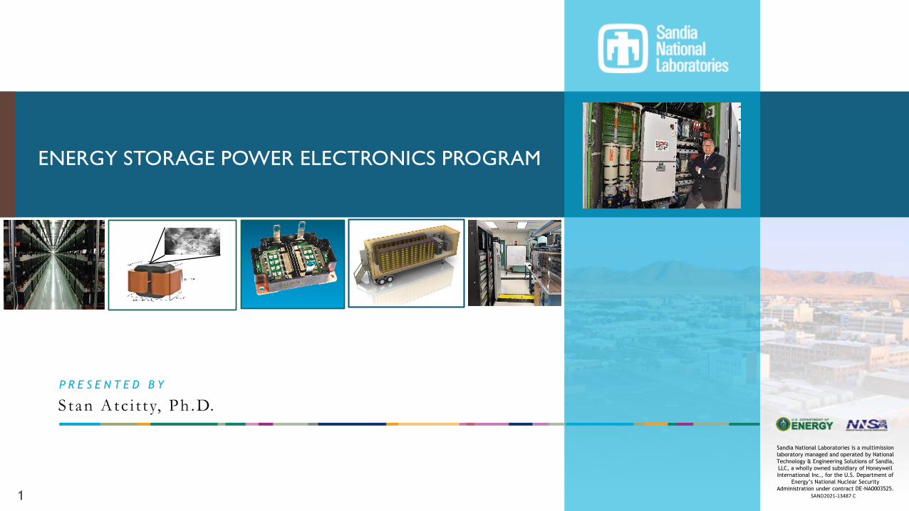
ENERGY STORAGE POWER ELECTRONICS PROGRAM
Stan Atc i t t y, Ph .D.
1 SAND2021-13487 C
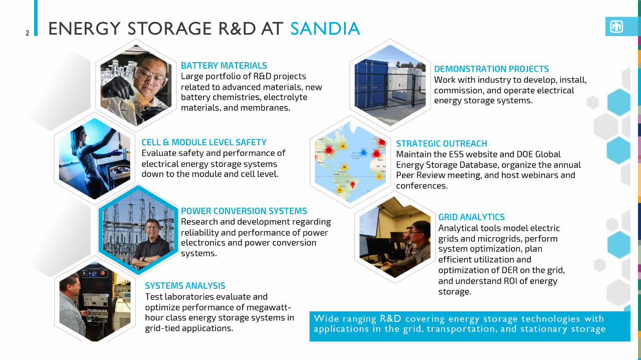
ENERGY STORAGE R&D AT SANDIA2

POWER CONVERSION SYSTEM – KEY ENABLING TECHNOLOGY3
-~ - ~
- ~
+ -
~~
+ -
-~
- ~
+ -+ -
- ~
Generation Transmission Sub-Transmission Distribution
HVDC
Hydro
Coal/Gas
Nuclear
Transformer
/ Substation
Energy Storage Energy StorageEnergy Storage
Industrial Load
Wind Power
Photovoltaic
Commercial Load
Residential
Load
Energy Storage
Power Conversion System

POWER CONVERSION SYSTEM4
▪ Power conversion systems (PCS), sometimes referred to and used interchangeably as power electronics, are a key enabling technology for energy storage.
▪ In a grid-tied energy storage system, the PCS controls the power supplied to and absorbed from the grid, simultaneously optimizing energy storage device performance and maintaining grid stability.
▪ There are multiple types of energy storage technologies, and each has their own characteristics and control parameters that must be managed by the PCS.
▪ An energy storage installation may be tasked with a variety of different grid support services; the PCS is responsible for controlling the flow of energy to meet the requirements of the intended grid support application.
▪ The major electrical components of a PCS are semiconductor switches, magnetic devices such as inductors and transformers, capacitors, and a controller.

ROLE OF SEMICONDUCTORS IN PCS 5
Semiconductor devices such as transistors and diodes are electronic components that rely on the internal material such as silicon for its function. For example:
▪ Transistors can become an open or short circuit based on the voltage level between the gate and source terminals. For a N-channel MOSFET, vgs > Vth turns ON the device.
▪ Diodes conduct only when there is a positive voltage between the anode and cathode terminals.
▪ Typically, semiconductor devices are made from Silicon (Si), but new wide bandgap (WBG) materials—such as Silicon Carbide (SiC) and Gallium Nitride (GaN)—are known for higher switching frequencies, higher blocking voltages, lower switching losses and higher junction temperatures than silicon-based switches.
▪ SiC (High Power): 650 V +
▪ GaN (Low Power): < 650 V, > 900V in development
▪ Reliability remains one of the major factors impeding the widespread adoption of WBG power devices; need to design, fabricate, and characterize WBG devices as a neutral third party.
▪ Battery electric vehicles will drive volumes up, cost down, and reliability up in the next 10 years.
▪ Electric grid is additional performance & reliability driver.
Resonant Dual Active Bridge (DAB)
DC-DC Converter
Three-phase DC-AC
inverter
Cr LrHFT
CLink
CAC
LACLFT
Csn
Rsn
Cin
a
b
c
+
-
+
-
S1
S2
S3
S4
S5
S6
S7
S8
S9
S10
S11
S12
S13
S14
Vp
+
-
Vin
Vs
+
-
AC Filter and LFT
+
-g
d
sN-Channel MOSFET
anode
cathode
Diode
Future of semiconductors:
▪ Lower on-resistance for given breakdown voltage
▪ Higher power density and increase efficiency
▪ Ultra WBG, Diamond
DC
DC
DC
AC
CLink
+
-
+
-
a
b
c
Low Frequency Transformer (LFT)
Power Conversion Systems
AC FiltersDC-AC Inverter
DC-DC Converter

ROLE OF MAGNETICS IN PCS 6
Inductors and transformers are passive elements formed by wires wound around magnetics components. Inductors store energy in an electro-magnetic field. Transformers transfer energy between primary and secondary windings wound around a magnetic material.
▪ Resonant inductors, Lr:
▪ Forms the converter resonant tank with Cr allowing zero-voltage or zero-current switching in the DC-DC converter stage.
▪ Usually Lr has a low magnitude.
▪ High-frequency transformer, HFT:
▪ HFT allows a higher voltage conversion ratio by selecting the required turns ratio, N.
▪ Compact footprint due to high frequency operation.
▪ AC filter inductors, LAC :
▪ Eliminate the harmonic distortion from the DC-AC inverter stage.
▪ Low-frequency transformer, LFT:
▪ Step-up or down the voltage from the PCS to the required level by selecting the necessary turns ratio N.
▪ LFTs are bulky since they operate at line frequency.
▪ Current magnetic materials do not meet all the requirements of emerging power electronics topologies.
▪ Significant volume reduction and increased reliability in PCS will be enabled by advanced magnetics.
Resonant Dual Active Bridge (DAB)
DC-DC Converter
Three-phase DC-AC
inverter
AC Filter and LFT
DC
DC
DC
AC
CLink
+
-
+
-
a
b
c
Low Frequency Transformer (LFT)
Power Conversion Systems
AC FiltersDC-AC Inverter
DC-DC Converter
Future of magnetics:
▪ High magnetization
▪ Low loss magnetic cores for high frequency transformers
▪ Nitrides and soft magnetic composites (SMC)
▪ AM 3D printed coresγ’-Fe4N magnetic core
DC
DC
DC
AC
CLink
+
-
+
-
a
b
c
Low Frequency Transformer (LFT)
Power Conversion Systems
AC FiltersDC-AC Inverter
DC-DC Converter
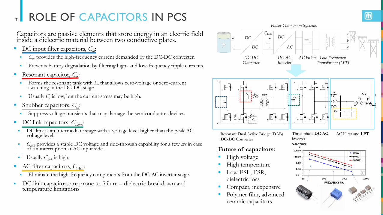
ROLE OF CAPACITORS IN PCS7
Capacitors are passive elements that store energy in an electric field inside a dielectric material between two conductive plates.
▪ DC input filter capacitors, Cin:
▪ Cin provides the high-frequency current demanded by the DC-DC converter.
▪ Prevents battery degradation by filtering high- and low-frequency ripple currents.
▪ Resonant capacitor, Cr :
▪ Forms the resonant tank with Lr that allows zero-voltage or zero-current switching in the DC-DC stage.
▪ Usually Cr is low, but the current stress may be high.
▪ Snubber capacitors, Csn:
▪ Suppress voltage transients that may damage the semiconductor devices.
▪ DC link capacitors, CLink:
▪ DC link is an intermediate stage with a voltage level higher than the peak AC voltage level.
▪ Clink provides a stable DC voltage and ride-through capability for a few ms in case of an interruption at AC input side.
▪ Usually Clink is high.
▪ AC filter capacitors, CAC :
▪ Eliminate the high-frequency components from the DC-AC inverter stage.
▪ DC-link capacitors are prone to failure – dielectric breakdown and temperature limitations
Resonant Dual Active Bridge (DAB)
DC-DC Converter
Three-phase DC-AC
inverter
AC Filter and LFT
Future of capacitors:
▪ High voltage
▪ High temperature
▪ Low ESL, ESR, dielectric loss
▪ Compact, inexpensive
▪ Polymer film, advanced ceramic capacitors

SYSTEM INTEGRATION8
New components are important, but not the whole story
▪ Advanced Topologies: ▪ Modular, fault-tolerant
hardware architectures
▪ Advanced Control Systems: ▪ Methods for detecting and
reacting to internal failures in real time
▪ Design-For-Reliability: ▪ Computational tools for
assessing reliability and remaining time-to-failure based on application-specific operating conditions
Thermal
Management
ControlEMC
System
ProtectionComms
Power
Module

9 POWER ELECTRONICS R&D IS HIERARICAL…
Semiconductor MaterialsMagnetic Materials
Capacitor Materials
Materials
▪ Bottom layer in the PE R&D spectrum (non-
application specific)
▪ Foundation for other technological
improvements
▪ Advanced semiconductor, magnetic materials,
new capacitor dielectrics, etc.
Components
▪ Materials are
combined together to
form components
▪ Basic building blocks
circuit
▪ Includes switches,
capacitors, inductors,
etc.
Subsystems
▪ Multiple components together
form subsystems
▪ Perform a specific task within
the PES
▪ Includes subsystem controls,
sensors, thermal management,
protection, power stage, etc.
(Power Electronics
System - PES)
Power Converter Modules
HVDC PCS Wind Energy PCS
PV PCS
Grid-tied Energy
Storage PCSElectric Vehicle
PCS
Systems
▪ Multiple subsystems together form the system or Power
Conversion System (PCS)
▪ Self-contained, fully functional unit that performs the
end-use application
▪ Includes DC/AC disconnects, system controls, final
packaging, etc.
Semiconductor Switches
CapacitorInductors and transformers
135µm
dielectric
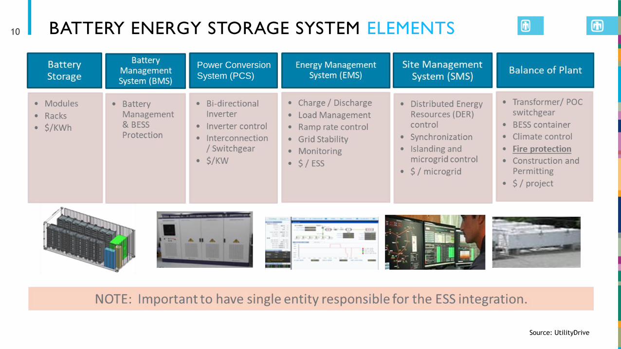
BATTERY ENERGY STORAGE SYSTEM ELEMENTS10
Source: UtilityDrive
Power Conversion
System (PCS)
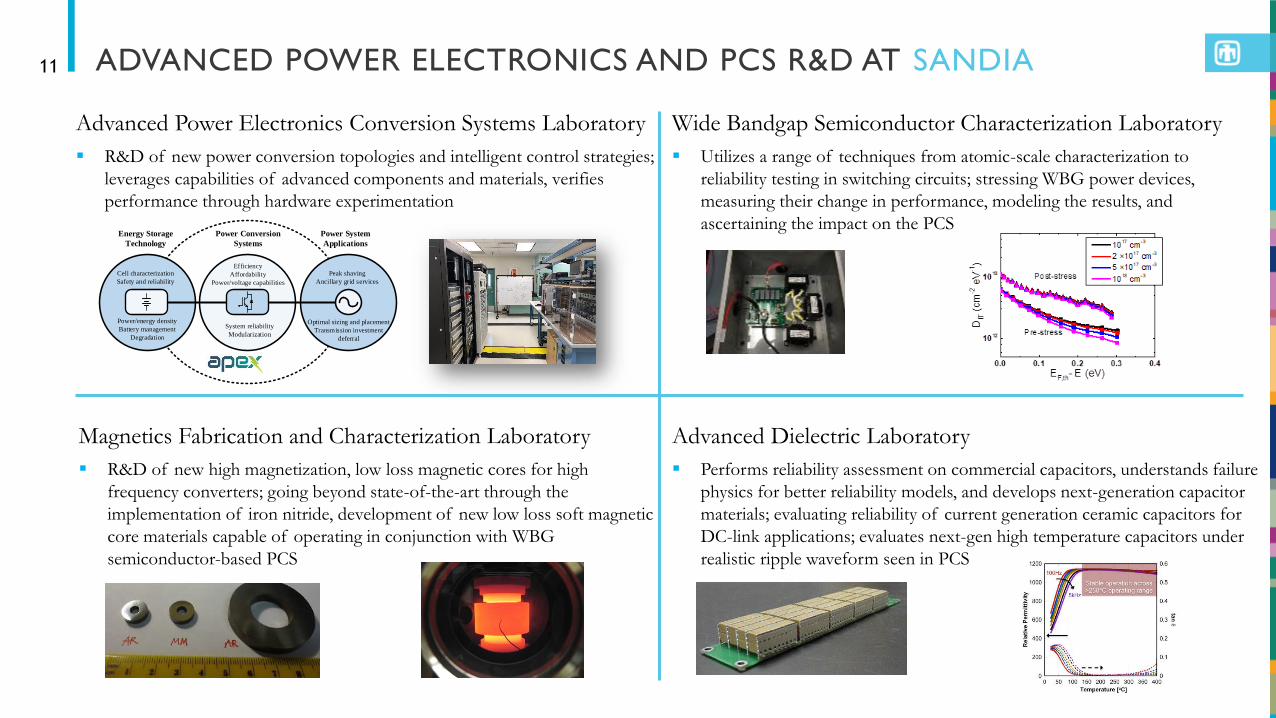
ADVANCED POWER ELECTRONICS AND PCS R&D AT SANDIA11
Energy Storage
Technology
Power Conversion
Systems
Power System
Applications
Cell characterization
Safety and reliability
Power/energy density
Battery management
Degradation
Peak shaving
Ancillary grid services
Optimal sizing and placement
Transmission investment
deferral
Efficiency
Affordability
Power/voltage capabilities
System reliability
Modularization
Advanced Power Electronics Conversion Systems Laboratory
▪ R&D of new power conversion topologies and intelligent control strategies;
leverages capabilities of advanced components and materials, verifies
performance through hardware experimentation
Wide Bandgap Semiconductor Characterization Laboratory
▪ Utilizes a range of techniques from atomic-scale characterization to
reliability testing in switching circuits; stressing WBG power devices,
measuring their change in performance, modeling the results, and
ascertaining the impact on the PCS
Magnetics Fabrication and Characterization Laboratory
▪ R&D of new high magnetization, low loss magnetic cores for high
frequency converters; going beyond state-of-the-art through the
implementation of iron nitride, development of new low loss soft magnetic
core materials capable of operating in conjunction with WBG
semiconductor-based PCS
Advanced Dielectric Laboratory
▪ Performs reliability assessment on commercial capacitors, understands failure
physics for better reliability models, and develops next-generation capacitor
materials; evaluating reliability of current generation ceramic capacitors for
DC-link applications; evaluates next-gen high temperature capacitors under
realistic ripple waveform seen in PCS

LOOKING FORWARD12
Ongoing Research Areas
▪ Power conversion system for scalable energy storage deployments▪ Modular topologies for direct MV grid connection
▪ Integration of storage in existing and emerging power electronic energy infrastructure
▪ Uninterruptible converter topologies for critical storage assets▪ Fault-tolerant and reconfigurable hardware architectures
▪ Hot-swap capable converters and storage systems
▪ Applications of power electronics in storage system safety▪ Stranded energy extraction
▪ Active response to thermal runaway
▪ Integration of advanced components▪ Wide bandgap devices
▪ Advanced magnetics
▪ Advanced capacitors
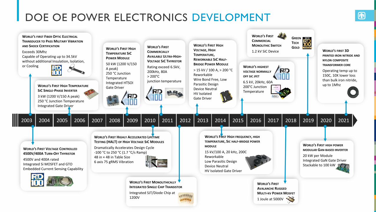
2003 2004 2005 2006 2007 2008 2009 2010 2011 2012 2013 2014 2015 2016 2017 2018 2019 2020 2021
13
WORLD’S FIRST HIGH TEMPERATURE
SIC SINGLE-PHASE INVERTER
3 kW (1200 V/150 A peak) 250 °C Junction TemperatureIntegrated Gate Driver
WORLD’S FIRST HIGH
VOLTAGE, HIGH
TEMPERATURE, REWORKABLE SIC HALF-BRIDGE POWER MODULE
> 15 kV / 100 A, > 200 °CReworkableWire Bond Free, Low Parasitic DesignDevice NeutralHV Isolated Gate Driver
WORLD’S FIRST HIGHLY ACCELERATED LIFETIME
TESTING (HALT) OF HIGH VOLTAGE SIC MODULES
Dramatically Accelerates Design Cycle-100 °C to 250 °C (1.7 °C/s Ramp)48 in × 48 in Table Size6 axis 75 gRMS Vibration
WORLD’S FIRST MONOLITHICALLY
INTEGRATED SINGLE CHIP TRANSISTOR
Integrated SJT/Diode Chip at 1200V
WORLD’S FIRST VOLTAGE CONTROLLED
4500V/400A TURN-OFF THYRISTOR
4500V and 400A ratedIntegrated Si MOSFET and GTO Embedded Current Sensing Capability
WORLD’S FIRST HIGH FREQUENCY, HIGH
TEMPERATURE, SIC HALF-BRIDGE POWER
MODULE
15 kV/100 A, 20 kHz, 200C ReworkableLow Parasitic DesignDevice NeutralHV Isolated Gate Driver
WORLD’S FIRST HIGH
TEMPERATURE SIC POWER MODULE
50 kW (1200 V/150 A peak) 250 °C Junction TemperatureIntegrated HTSOI Gate Driver
WORLD’S FIRST FIBER OPTIC ELECTRICAL
TRANSDUCER TO PASS MILITARY VIBRATION
AND SHOCK CERTIFICATION
Exceeds 30MhzCapable of Operating up to 34.5kV without additional Insulation, Isolation, or Cooling WORLD’S HIGHEST
VOLTAGE NORMALLY
OFF SIC JFET
6.5 kV, 20kHz, 60A 200°C Junction Temperature
WORLD’S FIRST
AVALANCHE RUGGED
MULTI-KV POWER MOSFET
1 Joule at 5000V
WORLD’S FIRST
COMMERCIALLY
AVAILABLE ULTRA-HIGH-VOLTAGE SIC THYRISTOR
Rating exceed 6.5kV, 200kHz, 80A > 200°C junction temperature
WORLD’S FIRST
COMMERCIAL
MONOLITHIC SWITCH
1.2 kV SiC Device
DOE OE POWER ELECTRONICS DEVELOPMENT
GREEN
TECH
GOLD
WORLD’S FIRST HIGH POWER
MODULAR GAN-BASED INVERTER
20 kW per ModuleIntegrated GaN Gate DriverStackable to 100 kW
WORLD’S FIRST 3D PRINTED IRON NITRIDE AND
NYLON COMPOSITE
TRANSFORMER CORE
Operating temp up to 150C, 10X lower loss than bulk iron nitride, up to 1Mhz
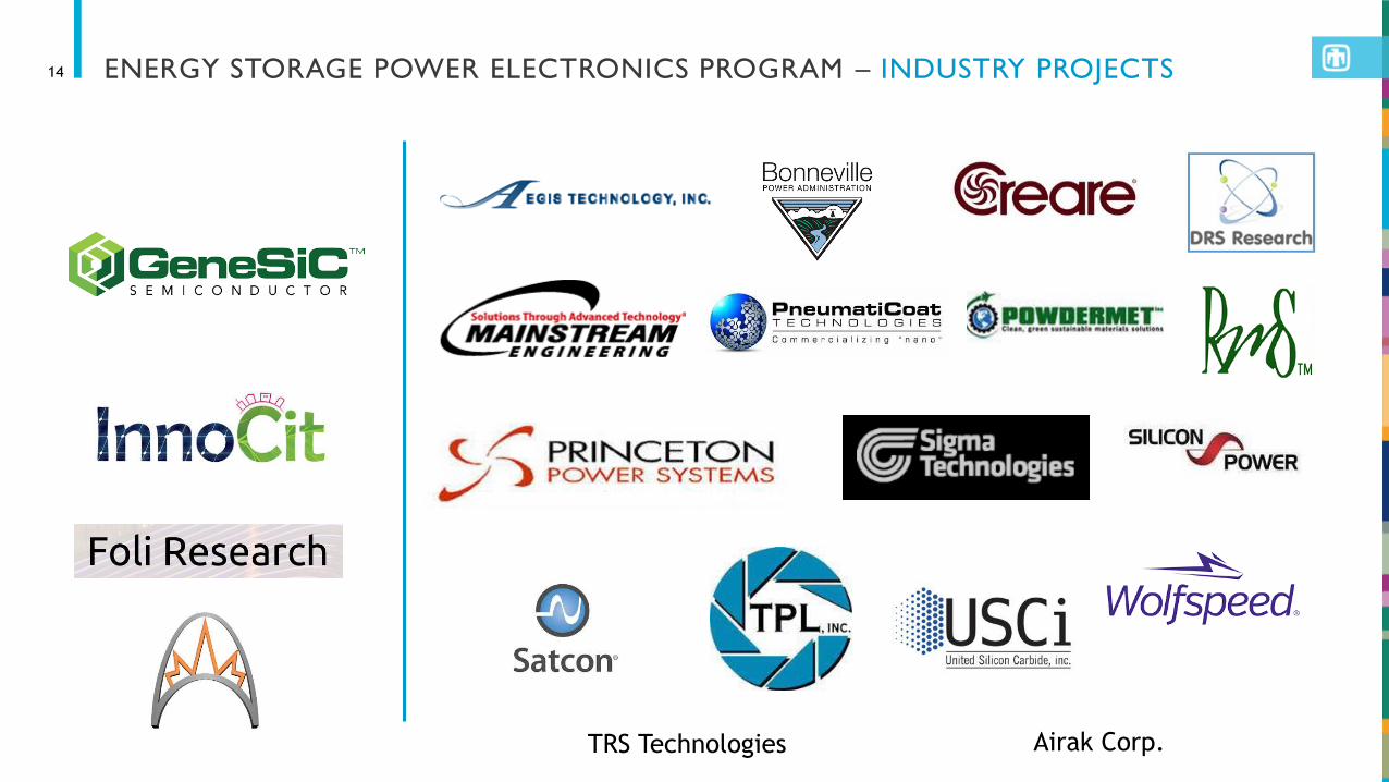
ENERGY STORAGE POWER ELECTRONICS PROGRAM – INDUSTRY PROJECTS14
TRS Technologies Airak Corp.

ENERGY STORAGE POWER ELECTRONICS PROGRAM – UNIVERSITY PROJECTS15
Questions?
Thank You !
The Energ y S to rage Power E lec t ron ics Prog ram i s suppor ted by Dr. Imre Gyuk and the Energ y S to rage Prog ram in the DOE Off i ce o f E lec t r i c i t y.